PWM Controlled3-Phase Inverter for Renewable Energy ... · phase inverter is highly suitable for...
12
Journal of Green Engineering, Vol. 9 2,189-200, Alpha Publishers This is an Open Access publication. © 2019 the Author(s). All rights reserved. 1 M. Venkatesan, 2 K Balachander, 3 S. G. Ramesh Kumar 1 Associate professor, Department of Electrical and Electronics Engineering, Vignan’s Lara Institute of Technology and Science, Guntur, Andra Pradesh, India. E-mail: [email protected] 2 Associate professor, Department of Electrical and Electronics Engineering, Karpagam Academy of Higher Education, Coimbatore, Tamilnadu, India. 3 Assistant professor, Department of Electrical and Electronics Engineering, FEAT, Annamalai University, Tamilnadu, India. Abstract In this article, Pulse Width Modulation (PWM) controlled 3-phase inverter for Renewable Energy (RES) Applications and environmental constraints are presented. The three-phase inverter with reduced components is realized in the solar PV applications. The optimized switching pattern of the inverter can be generated by comparing two reference signals to the single carrier frequency. The proposed three phase inverter is highly suitable for large solar power system Perturb and Observe (P&O) algorithm have been developed for the tracking of maximum power from the PV panel. A designed three-phase PV inverter has been demonstrated through MATLAB/ Simulink.The quality of the output voltage has been analyzed with respect to the THD. Finally, environmental factors of the solar PV system are investigated and other related impacts are discussed. Keywords: Three phase five level inverter, RES, PV, P&O, Environmental factors. 1 Introduction Renewable energy systems such as wind, solar are environmentally friendly and are used to produce green power. The India is one of the largest electrical power generations in the world about 6th place and 87.4% of power from thermal, hydroelectric, biomass and nuclear, etc. Only 12.6% of power is being generated from Renewable Energy Sources (RES) [1]. The government of India has been introduced the scheme “National Solar Mission (NSM) -2020” to promote the generation of PWM Controlled3-Phase Inverter for Renewable Energy Applications and Environmental Impacts Journal of Green Engineering (JGE) Volume-9, Issue-2, August 2019
Transcript of PWM Controlled3-Phase Inverter for Renewable Energy ... · phase inverter is highly suitable for...

Journal of Green Engineering, Vol. 9 2,189-200, Alpha Publishers This is an Open Access publication. © 2019 the Author(s). All rights reserved.
1M. Venkatesan, 2K Balachander, 3S. G. Ramesh Kumar 1Associate professor, Department of Electrical and Electronics Engineering, Vignan’s Lara Institute of Technology and Science, Guntur, Andra Pradesh, India. E-mail: [email protected] 2Associate professor, Department of Electrical and Electronics Engineering, Karpagam Academy of Higher Education, Coimbatore, Tamilnadu, India. 3Assistant professor, Department of Electrical and Electronics Engineering, FEAT, Annamalai University, Tamilnadu, India.
Abstract In this article, Pulse Width Modulation (PWM) controlled 3-phase inverter for Renewable Energy (RES) Applications and environmental constraints are presented. The three-phase inverter with reduced components is realized in the solar PV applications. The optimized switching pattern of the inverter can be generated by comparing two reference signals to the single carrier frequency. The proposed three phase inverter is highly suitable for large solar power system Perturb and Observe (P&O) algorithm have been developed for the tracking of maximum power from the PV panel. A designed three-phase PV inverter has been demonstrated through MATLAB/ Simulink.The quality of the output voltage has been analyzed with respect to the THD. Finally, environmental factors of the solar PV system are investigated and other related impacts are discussed.
Keywords: Three phase five level inverter, RES, PV, P&O, Environmental factors.
1 Introduction Renewable energy systems such as wind, solar are environmentally friendly and are used to produce green power. The India is one of the largest electrical power generations in the world about 6th place and 87.4% of power from thermal, hydroelectric, biomass and nuclear, etc. Only 12.6% of power is being generated from Renewable Energy Sources (RES) [1]. The government of India has been introduced the scheme “National Solar Mission (NSM) -2020” to promote the generation of
PWM Controlled3-Phase Inverter for Renewable Energy Applications and Environmental Impacts
Journal of Green Engineering (JGE)
Volume-9, Issue-2, August 2019
190 M.Venkatesan et. al.
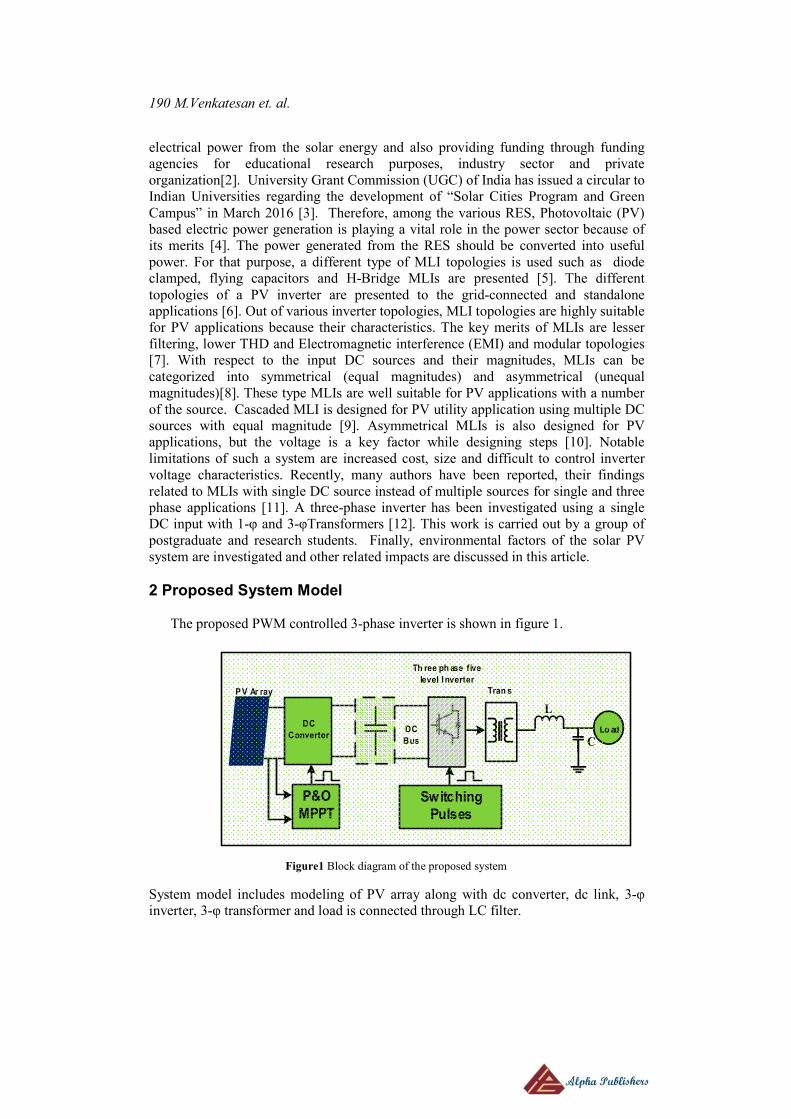
electrical power from the solar energy and also providing funding through funding agencies for educational research purposes, industry sector and private organization[2]. University Grant Commission (UGC) of India has issued a circular to Indian Universities regarding the development of “Solar Cities Program and Green Campus” in March 2016 [3]. Therefore, among the various RES, Photovoltaic (PV) based electric power generation is playing a vital role in the power sector because of its merits [4]. The power generated from the RES should be converted into useful power. For that purpose, a different type of MLI topologies is used such as diode clamped, flying capacitors and H-Bridge MLIs are presented [5]. The different topologies of a PV inverter are presented to the grid-connected and standalone applications [6]. Out of various inverter topologies, MLI topologies are highly suitable for PV applications because their characteristics. The key merits of MLIs are lesser filtering, lower THD and Electromagnetic interference (EMI) and modular topologies [7]. With respect to the input DC sources and their magnitudes, MLIs can be categorized into symmetrical (equal magnitudes) and asymmetrical (unequal magnitudes)[8]. These type MLIs are well suitable for PV applications with a number of the source. Cascaded MLI is designed for PV utility application using multiple DC sources with equal magnitude [9]. Asymmetrical MLIs is also designed for PV applications, but the voltage is a key factor while designing steps [10]. Notable limitations of such a system are increased cost, size and difficult to control inverter voltage characteristics. Recently, many authors have been reported, their findings related to MLIs with single DC source instead of multiple sources for single and three phase applications [11]. A three-phase inverter has been investigated using a single DC input with 1-φ and 3-φTransformers [12]. This work is carried out by a group of postgraduate and research students. Finally, environmental factors of the solar PV system are investigated and other related impacts are discussed in this article. 2 Proposed System Model The proposed PWM controlled 3-phase inverter is shown in figure 1.
Th ree ph ase five
level Inverter Tran s
DC
Bus
PV Ar ray
Lo ad
Switching Pulses
L
C
DC
Converter
P&O MPPT
Figure1 Block diagram of the proposed system
System model includes modeling of PV array along with dc converter, dc link, 3-φ inverter, 3-φ transformer and load is connected through LC filter.
PWM Controlled3-Phase Inverter for Renewable Energy Applications and Environmental Impacts 191
3 Design of PV System The light energy delivered by the sun is converted into electrical power and this process can be done by the solar cell. [13-14]The PV array is formed by connecting a solar panel series and parallel combinations. The TATA PB solar panel parameters have been used in the simulation purpose and verification of results. In general, PV inverter consists of a two stage, which includes dc-dc converter. The function is used to enhance the output voltage of the solar PV output and this is carried out by applying suitable duty cycle to a MOSFET. The DC converter operates at a higher frequency and the MOSFET is suitable for high frequency applications. PV panel parameters are given in Table 1.
Table 1 PV Panel Specifications (180W)
Specifications Rating
MPP Current (Imp) 5.03A
MPP Voltage (Vmp) 35.8V
Short circuit Current (Isc) 5.48A
Open circuit voltage (Voc) 43.6V
STC 25°C, 1000 W/m2, 1.5
Series resistance (Rs) 0.1133Ω
Design of single diode model PV cell and P&O algorithms has been applied for the proposed system to track power from the PV array. During the design of MPPT algorithms, the following panel parameters are considered such asvoltage and current rating of solar panel, power rating and Standard test conditions. The single diode based PV cell circuits and dc-dc converter is depicted in figs 2 and 3 respectively. Here, Rse and Rp are the values of series and parallel resistance respectively.
Figure 2 PV cell equivalent circuits

192 M.Venkatesan et. al.
Figure 3 Boost converter
The DC-DC converter is used to enhance the output voltage from the solar panel. Hence, it is necessary to connect the DC-DC converter in front of the inverter. The dc converter is controlled by PWM pulses and their control scheme is given in figure 4 and the operating principle of MPPT algorithms flow chart is found in figure 5. MPP result summary of simulation and experimental is given in Table 2.
Figure 4 DC converter control scheme
Table 2 MPP result summary: Simulation
Parameters Simulation results
Irradiance in W/m2 ��� ��� ����
1000 5.02 35.64 178.9
800 4.03 35.08 141.4
600 3.03 34.38 104.2
400 2.01 33.39 67.1
200 1.01 31.6 31.9

PWM Controlled3-Phase Inverter for Renewable Energy Applications and Environmental Impacts 193
Figure 5 P&O algorithm flow chart
Figure 6 shows the simulation results of a solar panel. Figure 6(a) shows that open circuit voltage against power (PV characteristics), it is noted that, the solar panel is generating the maximum power 180W at 1000�/�� irradiations, similarly 140W, 100W, 60W and 20W at 800�/��600�/��, 400�/�� , 200�/�� respectively. Figure 6 (b) shows I-V characteristics of the panel, it generates maximum current at1000�/��.
Figure 6(a) PV curves (b) I-V curves

194 M.Venkatesan et. al.
4 Three phase 5 level inverter The demonstration inverter is delivering power to the load through parallel connected three single phase five level inverters and its depicted in figure 7. The power is injected from the common dc link and voltage across the dc must greater than the required output voltage (At least 10-15% percentage of the required output voltage
(√2 × ���� ). In this power circuit three T-type single inverters are connected to a common dc link. The common dc link is constructed by series connection of two capacitors and equal values. The voltage across the each capacitor is half of the input voltage. The T-type inverter is constructed by H-bridge inverter and auxiliary inverter. Normally, H-bridge inverter consists of four IGBTs and out of these, Sa3 and Sa4 are operated at a rate of fundamental. The switches Sa1 and Sa2 and Sa5 in auxiliary circuits are operated at the rate of the carrier frequency. It is observed from figure 7 switches in phase A, Phase B, Phase C. All three phases are synthesis five level output voltage from the dc link voltage when gating pulses applied from the control circuit. Phase and neutral of each phase are connected to the corresponding to the transformer of the primary winding and neutral point of all phases is shorted. The voltages delivered by the parallel connected five level inverters are fed to the primary terminals of the transformer. Onthe output side of the transformer is connected in star and then it is fed to the load through LC filter.
Figure 7 Power circuit diagram

PWM Controlled3-Phase Inverter for Renewable Energy Applications and Environmental Impacts 195
4.1 Modes of Operation The PWM controlled Inverter has been designed with 15 active switches and 12 diodes and it is shown in figure 8. In this work, three single-phase inverters are connected in parallel and each consists of the auxiliary inverter (20 KHz) and H bridge inverter (50Hz), so that, each single-phase inverter consists of 15 active switches and 12 diodes. Table 3 is shown switching conditions of the inverter.The inverter is tested in open loop mode using PWM control schemes. In case. If the load of the inverter is increased, DC link voltage slightly decreased.
Sa1
Sa2 Sa4
Sa3
Sa5
C1
C2
Sa1
Sa2 Sa4
Sa3
Sa5
C1
C2
Sa1
Sa2 Sa4
Sa3
Sa5
C1
C2
LoadLoad
Load
Sa1
Sa2 Sa4
Sa3
Sa5
C1
C2
Load
State 1:V=+Vo
State 4:V=-Vo
State 2:V=+Vo/2
State 3:V=-Vo/2
Figure 8 Modes of operation
5 Results and Discussion In this section, the simulation results of the proposed inverter are presented and obtained results are verified through MATLAB simulation studies
Figure 9 Switching pulses
196 M.Venkatesan et. al.
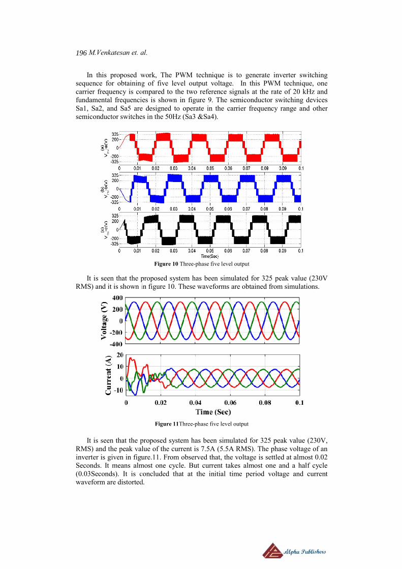
In this proposed work, The PWM technique is to generate inverter switching sequence for obtaining of five level output voltage. In this PWM technique, one carrier frequency is compared to the two reference signals at the rate of 20 kHz and fundamental frequencies is shown in figure 9. The semiconductor switching devices Sa1, Sa2, and Sa5 are designed to operate in the carrier frequency range and other semiconductor switches in the 50Hz (Sa3 &Sa4).
It is seen that the proposed system RMS) and it is shown in figure 10. These waveforms are obtained from simulations.
It is seen that the proposed system RMS) and the peak value of the current is 7.5A inverter is given in figureSeconds. It means almost one cycle. But current takes almost one and a (0.03Seconds). It is concluded waveform are distorted.
et. al.
In this proposed work, The PWM technique is to generate inverter switching ce for obtaining of five level output voltage. In this PWM technique, one
carrier frequency is compared to the two reference signals at the rate of 20 kHz and fundamental frequencies is shown in figure 9. The semiconductor switching devices
Sa5 are designed to operate in the carrier frequency range and other semiconductor switches in the 50Hz (Sa3 &Sa4).
Figure 10 Three-phase five level output
the proposed system has been simulated for 325 peak value (230V ) and it is shown in figure 10. These waveforms are obtained from simulations.
Figure 11Three-phase five level output
the proposed system has been simulated for 325 peak value (230V,
value of the current is 7.5A (5.5A RMS). The phase voltage oinverter is given in figure.11. From observed that, the voltage is settled at almost 0.02 Seconds. It means almost one cycle. But current takes almost one and a
. It is concluded that at the initial time period voltage and current waveform are distorted.
In this proposed work, The PWM technique is to generate inverter switching ce for obtaining of five level output voltage. In this PWM technique, one
carrier frequency is compared to the two reference signals at the rate of 20 kHz and fundamental frequencies is shown in figure 9. The semiconductor switching devices
Sa5 are designed to operate in the carrier frequency range and other
been simulated for 325 peak value (230V ) and it is shown in figure 10. These waveforms are obtained from simulations.
been simulated for 325 peak value (230V, ). The phase voltage of an
that, the voltage is settled at almost 0.02 Seconds. It means almost one cycle. But current takes almost one and a half cycle
time period voltage and current
PWM Controlled3-Phase Inverter for Renewable Energy Applications and Environmental Impacts 197
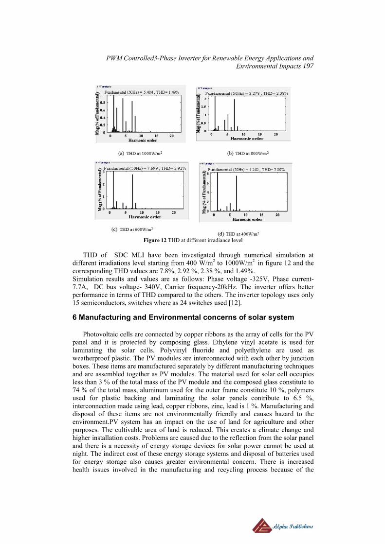
Figure 12 THD at different irradiance level
THD of SDC MLI have been investigated through numerical simulation at different irradiations level starting from 400 W/m2 to 1000W/m2 in figure 12 and the corresponding THD values are 7.8%, 2.92 %, 2.38 %, and 1.49%. Simulation results and values are as follows: Phase voltage -325V, Phase current- 7.7A, DC bus voltage- 340V, Carrier frequency-20kHz. The inverter offers better performance in terms of THD compared to the others. The inverter topology uses only 15 semiconductors, switches where as 24 switches used [12].
6 Manufacturing and Environmental concerns of solar system Photovoltaic cells are connected by copper ribbons as the array of cells for the PV panel and it is protected by composing glass. Ethylene vinyl acetate is used for laminating the solar cells. Polyvinyl fluoride and polyethylene are used as weatherproof plastic. The PV modules are interconnected with each other by junction boxes. These items are manufactured separately by different manufacturing techniques and are assembled together as PV modules. The material used for solar cell occupies less than 3 % of the total mass of the PV module and the composed glass constitute to 74 % of the total mass, aluminum used for the outer frame constitute 10 %, polymers used for plastic backing and laminating the solar panels contribute to 6.5 %, interconnection made using lead, copper ribbons, zinc, lead is 1 %. Manufacturing and disposal of these items are not environmentally friendly and causes hazard to the environment.PV system has an impact on the use of land for agriculture and other purposes. The cultivable area of land is reduced. This creates a climate change and higher installation costs. Problems are caused due to the reflection from the solar panel and there is a necessity of energy storage devices for solar power cannot be used at night. The indirect cost of these energy storage systems and disposal of batteries used for energy storage also causes greater environmental concern. There is increased health issues involved in the manufacturing and recycling process because of the

198 M.Venkatesan et. al.
usage of toxic chemicals. The efficiency and payback of the PV panels are based on the irradiation, the location at which it is installed, energy used in the manufacturing process, shadowing. Mono-crystalline has the largest payback period because of the cost involved in manufacturing. Recycling the exhausted PV modules is a great challenge since different materials are assembled to a PV panel. The damaged solar panels can be rectified by chemical etching process. Materials such as glass and aluminum are recycled. 7 Conclusion The simulation study of 3-phase 5-level inverter for RES applications and environmental constraints have been presented in this paper.The optimized switching pattern of the inverter can be generated by comparing two reference signals to the single carrier frequency. Perturb and Observe (P&O) algorithm have been developed for the tracking of maximum power from the PV panel. A designed three-phase PV inverter has been demonstrated through MATLAB simulation. Finally environment factors of the solar PV and other related impacts have been discussed
References [1] http://indianpowersector.com [2] Government of India, Ministry of New and Renewable Energy,
www.mnre.gov.in. [3] Development of Solar Cities Programme, Government of India,
www.mnre.gov.in [4] Z. Jacek, B. Sebastian, M. Piotr, B. Mateusz, et al. “The laboratory stand for
measurements and analysis of photovoltaic modules”, International Journal of Electrical Engineering Education, pp. 1–13, 2018.
[5] O. Javad, K. Masoumeh, “THD Minimization in Multilevel Inverters using Teaching-Learning-Based Optimization Algorithm”, International Journal of Ambient Energy, Accepted for publications, DOI: 10.1080/01430750.2017. 1298057, 2017.
[6] N. Prabaharan, and K. Palanisamy , “Analysis and integration of multilevel inverter configuration with boost converters in a photovoltaic system”, Energy Conversion and Management, Vol.128, pp. 327–342, 2016.
[7] I. A. Harbi, H. Z. Azazi, A. E. Lashine, A. E. Elsabbe, et al. ,"A higher levels multilevel inverter with reduced number of switches', International Journal of Electronics, (Taylor and Francis), Vol. 105, No. 8, pp.1286–1299, 2018.
[8] I. Colak, E. Kabalci, R. Bayindir, et al. , “Review of multilevel voltage source inverter topologies and control schemes,” Energy Conversion and Management , Vol.52, No.2, pp.1114-1128, 2011.
[9] KK. Gupta and S. Jain, “Comprehensive review of a recently proposed multilevel inverter”, IET Power Electronics, pp. 467–79, 2014.
[10] E. Zamiri, HM. Kojabadi, R. Barzegarkhoo, N. Vosoughi, L. Chang, et al., “Cascaded multilevel inverter using series connection of novel capacitor-based units with minimum switch count”, IET Power Electronics, pp.2060–75, 2016.
[11] Jiwanjot Singh, RatnaDahiya, Lalit Mohan Saini, et al., “Recent research on transformer based single DC source multilevel inverter: A review”, Renewable and Sustainable Energy Reviews, 2017.

PWM Controlled3-Phase Inverter for Renewable Energy Applications and Environmental Impacts 199
[12] A. K. Panda, Y. Suresh , “Performance of cascaded multilevel inverter by employing single and three-phase transformers”, IET Power Electronics, Vol. 5, No.9, pp.1694–1705, 2012.
[13] S.Subramaniam, B.Akash, R.Vignesh et al., “Design and Implementation of Three Phase Micro Inverter Based PV Module”, Journal of Green Engineering, Vol. 9, No.1, pp. 35-59, 2019.
[14] Ranjith Kumar Kalilasam, Venkatesan Mani, “FPGA based quasi z-source cascaded multilevel inverter using multi-carrier PWM techniques”, Journal of Vibro engineering, Vol.20, No.3, pp. 1544-1553, 2018.
Biographies
M Venkatesan received his B.E., in ECE from Anna University, Chennai, Tamil Nadu, India, in 2008, and his M.E., in Power Electronics and Drives from Government College of Technology, Coimbatore, Tamil Nadu, India, in 2010. He completed his Ph.D in Power Electronics from Anna University, Chennai, Tamil Nadu, India, in 2017. At present, he is Associate professor of Electrical and Electronics Engineering, Vignan’s Lara Institute of Technology and Science, Vadlmudi, Andhra Pradesh, India.
K. Balachander received the Diploma in EEE from PSG Polytechnic, Coimbatore in 1993 and Bachelor degree in Electrical and Electronics Engineering from Coimbatore Institute of Technology, Coimbatore in 2001. He acquired M.E in VLSI Design from Anna University Coimbatore in 2009 and doctorate in Electrical and Electronics Engineering from Karpagam Academy of Higher Education, Karpagam University, Coimbatore in 2017.

200 M.Venkatesan et. al.
S. G. Ramesh kumar has completed BE (EEE) in the year 1999 and subsequently completed his ME(Applied Electronics) in the 2001at Coimbatore Institute of Technology and joined as a lecturer in The Department of Electrical Engineering,FEAT, Annamalai University in the year of 2003. Simutaneously,He worked as a course Coordinator for Sinmax global solutions for VLSI-Ecad training program in Annamalai University.His area of interest in the Field of VLSI,Signals and Systems and Digital Signal processing,IoT,and Wireless Sensor Networks.Published Papers in Wireless Sensor networks, IoT agriculture Applications.Prasented papers in international conference in the area of DC drives,Wireless mobile AdHoc Networks.Currently Persuing PhD in the area of Various attacks and Routing procedures in WSN.Now He is working as an Asst Professor in Electrical Engg, FEAT, Annamalai University (On deputation as Lecturer and HOD I/C Department of Electrical Engg, Government Polytechnic College, Coimbatore-14)