PSpice for Digital Communications...
72
PSpice for Digital Communications Engineering
Transcript of PSpice for Digital Communications...

MOBK066-FM MOBKXXX-Sample.cls March 15, 2007 21:30
PSpice for DigitalCommunications Engineering

MOBK066-FM MOBKXXX-Sample.cls March 15, 2007 21:30
Copyright © 2007 by Morgan & Claypool
All rights reserved. No part of this publication may be reproduced, stored in a retrieval system, or transmitted inany form or by any means—electronic, mechanical, photocopy, recording, or any other except for brief quotationsin printed reviews, without the prior permission of the publisher.
PSpice for Digital Communications Engineering
Paul Tobin
www.morganclaypool.com
ISBN: 1598291629 paperbackISBN: 9781598291629 paperback
ISBN: 1598291637 ebookISBN: 9781598291636 ebook
DOI 10.2200/S00072ED1V01Y200612DCS010
A Publication in the Morgan & Claypool Publishers seriesSYNTHESIS LECTURES ON DIGITAL CIRCUITS AND SYSTEMS #10
Lecture #10Series Editor: Mitchell A. Thornton, Southern Methodist University
Library of Congress Cataloging-in-Publication Data
Series ISSN: 1932-3166 printSeries ISSN: 1932-3174 electronic
First Edition
10 9 8 7 6 5 4 3 2 1

MOBK066-FM MOBKXXX-Sample.cls March 15, 2007 21:30
PSpice for DigitalCommunications EngineeringPaul TobinSchool of Electronic and Communications EngineeringDublin Institute of TechnologyIreland
SYNTHESIS LECTURES ON DIGITAL CIRCUITS AND SYSTEMS #10
M&C M o r g a n & C l a y p o o l P u b l i s h e r s

MOBK066-FM MOBKXXX-Sample.cls March 15, 2007 21:30
iv
ABSTRACTPSpice for Digital Communications Engineering shows how to simulate digital communicationsystems and modulation methods using the very powerful Cadence Orcad PSpice version 10.5suite of software programs. Fourier series and Fourier transform are applied to signals to setthe ground work for the modulation techniques introduced in later chapters. Various basebandsignals, including duo-binary baseband signaling, are generated and the spectra are examinedto detail the unsuitability of these signals for accessing the public switched network. Pulsecode modulation and time-division multiplexing circuits are examined and simulated wheresampling and quantization noise topics are discussed. We construct a single-channel PCMsystem from transmission to receiver i.e. end-to-end, and import real speech signals to examinethe problems associated with aliasing, sample and hold.
Companding is addressed here and we look at the A and mu law characteristics forachieving better signal to quantization noise ratios. Several types of delta modulators areexamined and also the concept of time division multiplexing is considered. Multi-level signalingtechniques such as QPSK and QAM are analyzed and simulated and ‘home-made meters’, suchas scatter and eye meters, are used to assess the performance of these modulation systems inthe presence of noise. The raised-cosine family of filters for shaping data before transmissionis examined in depth where bandwidth efficiency and channel capacity is discussed. We plotseveral graphs in Probe to compare the efficiency of these systems. Direct spread spectrum isthe last topic to be examined and simulated to show the advantages of spreading the signal overa wide bandwidth and giving good signal security at the same time.
KEYWORDSFourier series and Fourier transforms, baseband and passband modulation, pulse code mod-ulation, time-division multiplexing, quantization noise, M-ary signaling, QPSK, QAM, eye-meter, scatter diagrams, spread spectrum, raised cosine filter.

MOBK066-FM MOBKXXX-Sample.cls March 15, 2007 21:30
I would like to dedicate this book to my wife and friend,Marie and sons Lee, Roy, Scott and Keith and my
parents (Eddie and Roseanne), sisters, Sylvia,Madeleine, Jean, and brother, Ted.

MOBK066-FM MOBKXXX-Sample.cls March 15, 2007 21:30

MOBK066-FM MOBKXXX-Sample.cls March 15, 2007 21:30
vii
ContentsPreface . . . . . . . . . . . . . . . . . . . . . . . . . . . . . . . . . . . . . . . . . . . . . . . . . . . . . . . . . . . . . . . . . . . . . . . xi
1. Fourier Analysis, Signals, and Bandwidth . . . . . . . . . . . . . . . . . . . . . . . . . . . . . . . . . . . . . . . 11.1 Digital Signals . . . . . . . . . . . . . . . . . . . . . . . . . . . . . . . . . . . . . . . . . . . . . . . . . . . . . . . . . . . 11.2 Bandwidth . . . . . . . . . . . . . . . . . . . . . . . . . . . . . . . . . . . . . . . . . . . . . . . . . . . . . . . . . . . . . . .21.3 Pulse Spectra for Different Pulse Widths and Period . . . . . . . . . . . . . . . . . . . . . . . . . 2
1.3.1 Average and RMS Pulse Power . . . . . . . . . . . . . . . . . . . . . . . . . . . . . . . . . . . . 31.3.2 Unsynchronizing Probe–Plot Axis . . . . . . . . . . . . . . . . . . . . . . . . . . . . . . . . . . 41.3.3 Fourier Transform . . . . . . . . . . . . . . . . . . . . . . . . . . . . . . . . . . . . . . . . . . . . . . . . 61.3.4 Fourier Series Analysis . . . . . . . . . . . . . . . . . . . . . . . . . . . . . . . . . . . . . . . . . . . . 8
1.4 The Vector Part . . . . . . . . . . . . . . . . . . . . . . . . . . . . . . . . . . . . . . . . . . . . . . . . . . . . . . . . . 111.5 Exercise . . . . . . . . . . . . . . . . . . . . . . . . . . . . . . . . . . . . . . . . . . . . . . . . . . . . . . . . . . . . . . . . 13
2. Baseband Transmission Techniques . . . . . . . . . . . . . . . . . . . . . . . . . . . . . . . . . . . . . . . . . . . 152.1 Baseband Signals . . . . . . . . . . . . . . . . . . . . . . . . . . . . . . . . . . . . . . . . . . . . . . . . . . . . . . . . 152.2 Baseband Signal Formats . . . . . . . . . . . . . . . . . . . . . . . . . . . . . . . . . . . . . . . . . . . . . . . . 15
2.2.1 NonReturn to Zero (NRZ) Coding. . . . . . . . . . . . . . . . . . . . . . . . . . . . . . . .162.2.2 FileStim Generator . . . . . . . . . . . . . . . . . . . . . . . . . . . . . . . . . . . . . . . . . . . . . . 162.2.3 NRZ-B . . . . . . . . . . . . . . . . . . . . . . . . . . . . . . . . . . . . . . . . . . . . . . . . . . . . . . . . . 17
2.3 RZ Encoding and Decoding . . . . . . . . . . . . . . . . . . . . . . . . . . . . . . . . . . . . . . . . . . . . . 182.3.1 RZ to NRZ Decoder . . . . . . . . . . . . . . . . . . . . . . . . . . . . . . . . . . . . . . . . . . . . . 19
2.4 Manchester Encoding and Decoding . . . . . . . . . . . . . . . . . . . . . . . . . . . . . . . . . . . . . . 212.4.1 Manchester Unipolar to BipolarEncoding . . . . . . . . . . . . . . . . . . . . . . . . . . 212.4.2 Manchester (Biphase) Decoding . . . . . . . . . . . . . . . . . . . . . . . . . . . . . . . . . . 232.4.3 Differential Manchester Coding . . . . . . . . . . . . . . . . . . . . . . . . . . . . . . . . . . . 24
2.5 Alternate Mark Inversion Encoding . . . . . . . . . . . . . . . . . . . . . . . . . . . . . . . . . . . . . . . 252.5.1 AMI Decoding . . . . . . . . . . . . . . . . . . . . . . . . . . . . . . . . . . . . . . . . . . . . . . . . . . 25
2.6 DUO-Binary Baseband Signaling . . . . . . . . . . . . . . . . . . . . . . . . . . . . . . . . . . . . . . . . . 272.6.1 Use of a Precoder in Duo-Binary Signaling . . . . . . . . . . . . . . . . . . . . . . . . . 29
2.7 Integrate and Dump Matched Filter Baseband Receiver . . . . . . . . . . . . . . . . . . . . . 302.7.1 Example . . . . . . . . . . . . . . . . . . . . . . . . . . . . . . . . . . . . . . . . . . . . . . . . . . . . . . . . 32
2.8 Exercises . . . . . . . . . . . . . . . . . . . . . . . . . . . . . . . . . . . . . . . . . . . . . . . . . . . . . . . . . . . . . . . 34

MOBK066-FM MOBKXXX-Sample.cls March 15, 2007 21:30
viii PSPICE FOR DIGITAL COMMUNICATIONS ENGINEERING
3. Sampling and Pulse Code Modulation . . . . . . . . . . . . . . . . . . . . . . . . . . . . . . . . . . . . . . . . . 373.1 Single-Channel Pulse Code Modulation . . . . . . . . . . . . . . . . . . . . . . . . . . . . . . . . . . . 373.2 Companding Characteristics . . . . . . . . . . . . . . . . . . . . . . . . . . . . . . . . . . . . . . . . . . . . . 383.3 Sampling . . . . . . . . . . . . . . . . . . . . . . . . . . . . . . . . . . . . . . . . . . . . . . . . . . . . . . . . . . . . . . . 41
3.3.1 Sallen and Key Antialiasing Active Filter . . . . . . . . . . . . . . . . . . . . . . . . . . . 423.3.2 Speech Signals . . . . . . . . . . . . . . . . . . . . . . . . . . . . . . . . . . . . . . . . . . . . . . . . . . .443.3.3 Sample and Hold . . . . . . . . . . . . . . . . . . . . . . . . . . . . . . . . . . . . . . . . . . . . . . . . 45
3.4 Quantization Noise . . . . . . . . . . . . . . . . . . . . . . . . . . . . . . . . . . . . . . . . . . . . . . . . . . . . . .493.5 Analog to Digital Conversion . . . . . . . . . . . . . . . . . . . . . . . . . . . . . . . . . . . . . . . . . . . . 50
3.5.1 DAC Resolution . . . . . . . . . . . . . . . . . . . . . . . . . . . . . . . . . . . . . . . . . . . . . . . . 513.5.2 Band-Stop Filter . . . . . . . . . . . . . . . . . . . . . . . . . . . . . . . . . . . . . . . . . . . . . . . . .52
3.6 Pulse Code Modulation . . . . . . . . . . . . . . . . . . . . . . . . . . . . . . . . . . . . . . . . . . . . . . . . . . 533.6.1 Universal Shift Register . . . . . . . . . . . . . . . . . . . . . . . . . . . . . . . . . . . . . . . . . . 543.6.2 74194 Universal Shift Register . . . . . . . . . . . . . . . . . . . . . . . . . . . . . . . . . . . . 55
3.7 Single-Channel 4-Bit PCM Transmitter . . . . . . . . . . . . . . . . . . . . . . . . . . . . . . . . . . 563.8 Time-Division Multiplexing and Demultiplexing. . . . . . . . . . . . . . . . . . . . . . . . . . .58
3.8.1 Time-division Multiplexing of Two PAM Signals . . . . . . . . . . . . . . . . . . 583.9 Linear Delta Modulation . . . . . . . . . . . . . . . . . . . . . . . . . . . . . . . . . . . . . . . . . . . . . . . . 60
3.9.1 Delta Demodulation . . . . . . . . . . . . . . . . . . . . . . . . . . . . . . . . . . . . . . . . . . . . .643.10 Exercises . . . . . . . . . . . . . . . . . . . . . . . . . . . . . . . . . . . . . . . . . . . . . . . . . . . . . . . . . . . . . . . 64
4. Passband Transmission Techniques . . . . . . . . . . . . . . . . . . . . . . . . . . . . . . . . . . . . . . . . . . . 714.1 Baseband to Passband . . . . . . . . . . . . . . . . . . . . . . . . . . . . . . . . . . . . . . . . . . . . . . . . . . . 714.2 Amplitude Shift Keying. . . . . . . . . . . . . . . . . . . . . . . . . . . . . . . . . . . . . . . . . . . . . . . . . .714.3 Frequency Shift Keying . . . . . . . . . . . . . . . . . . . . . . . . . . . . . . . . . . . . . . . . . . . . . . . . . . 73
4.3.1 Frequency Shift Keying Spectrum . . . . . . . . . . . . . . . . . . . . . . . . . . . . . . . . . 744.3.2 FSK Receiver . . . . . . . . . . . . . . . . . . . . . . . . . . . . . . . . . . . . . . . . . . . . . . . . . . . .754.3.3 Infinite Gain Multiple Feedback Active Filter . . . . . . . . . . . . . . . . . . . . . . 77
4.4 Phase Shift Keying . . . . . . . . . . . . . . . . . . . . . . . . . . . . . . . . . . . . . . . . . . . . . . . . . . . . . . 794.4.1 PSK Receiver . . . . . . . . . . . . . . . . . . . . . . . . . . . . . . . . . . . . . . . . . . . . . . . . . . . .84
4.5 Differential Phase Shift Keying (DPSK) . . . . . . . . . . . . . . . . . . . . . . . . . . . . . . . . . . . 864.6 Differential Phase Shift Receiver . . . . . . . . . . . . . . . . . . . . . . . . . . . . . . . . . . . . . . . . . .894.7 Exercises . . . . . . . . . . . . . . . . . . . . . . . . . . . . . . . . . . . . . . . . . . . . . . . . . . . . . . . . . . . . . . . 91
5. Multilevel Signaling and Bandwidth Efficiency . . . . . . . . . . . . . . . . . . . . . . . . . . . . . . . . . 935.1 Channel Capacity . . . . . . . . . . . . . . . . . . . . . . . . . . . . . . . . . . . . . . . . . . . . . . . . . . . . . . . 935.2 Multilevel Encoding: Bandwidth Efficiency . . . . . . . . . . . . . . . . . . . . . . . . . . . . . . . . 945.3 Bit Error Rate . . . . . . . . . . . . . . . . . . . . . . . . . . . . . . . . . . . . . . . . . . . . . . . . . . . . . . . . . . 95

MOBK066-FM MOBKXXX-Sample.cls March 15, 2007 21:30
PSPICE FOR DIGITAL COMMUNICATIONS ENGINEERING ix
5.4 Quadrature Phase Shift Keying . . . . . . . . . . . . . . . . . . . . . . . . . . . . . . . . . . . . . . . . . . . 965.5 QPSK Modulation Using ABM Parts . . . . . . . . . . . . . . . . . . . . . . . . . . . . . . . . . . . . . 97
5.5.1 QPSK Modulation Using a Bit-Splitter . . . . . . . . . . . . . . . . . . . . . . . . . . . . 985.5.2 QPSK Receiver . . . . . . . . . . . . . . . . . . . . . . . . . . . . . . . . . . . . . . . . . . . . . . . . .101
5.6 Offset Quadrature Phase Shift Keying. . . . . . . . . . . . . . . . . . . . . . . . . . . . . . . . . . . .1025.7 Gaussian Minimum Shift Keying . . . . . . . . . . . . . . . . . . . . . . . . . . . . . . . . . . . . . . . 1065.8 Eight-PSK . . . . . . . . . . . . . . . . . . . . . . . . . . . . . . . . . . . . . . . . . . . . . . . . . . . . . . . . . . . . 1075.9 Quadrature Amplitude Modulation . . . . . . . . . . . . . . . . . . . . . . . . . . . . . . . . . . . . . . 110
5.9.1 Eight-QAM . . . . . . . . . . . . . . . . . . . . . . . . . . . . . . . . . . . . . . . . . . . . . . . . . . . 1125.9.2 Comparison of PSK and QAM . . . . . . . . . . . . . . . . . . . . . . . . . . . . . . . . . . 1125.9.3 Sixteen-Quadrature Amplitude Modulation . . . . . . . . . . . . . . . . . . . . . . . 1145.9.4 Two-to-Four Level Conversion . . . . . . . . . . . . . . . . . . . . . . . . . . . . . . . . . . 116
5.10 Clock Extraction . . . . . . . . . . . . . . . . . . . . . . . . . . . . . . . . . . . . . . . . . . . . . . . . . . . . . . . 1165.11 Costas Loop . . . . . . . . . . . . . . . . . . . . . . . . . . . . . . . . . . . . . . . . . . . . . . . . . . . . . . . . . . . 1205.12 Exercises . . . . . . . . . . . . . . . . . . . . . . . . . . . . . . . . . . . . . . . . . . . . . . . . . . . . . . . . . . . . . . 122
6. System Performance and Test Instruments. . . . . . . . . . . . . . . . . . . . . . . . . . . . . . . . . . . . 1276.1 Noise Generator . . . . . . . . . . . . . . . . . . . . . . . . . . . . . . . . . . . . . . . . . . . . . . . . . . . . . . . 1276.2 Eye Diagram . . . . . . . . . . . . . . . . . . . . . . . . . . . . . . . . . . . . . . . . . . . . . . . . . . . . . . . . . . 127
6.2.1 The Eye Meter . . . . . . . . . . . . . . . . . . . . . . . . . . . . . . . . . . . . . . . . . . . . . . . . . 1286.2.2 Eye Diagram Application . . . . . . . . . . . . . . . . . . . . . . . . . . . . . . . . . . . . . . . 129
6.3 Vector/Scatter Diagram. . . . . . . . . . . . . . . . . . . . . . . . . . . . . . . . . . . . . . . . . . . . . . . . .1316.3.1 Noisy QPSK Scatter Diagram . . . . . . . . . . . . . . . . . . . . . . . . . . . . . . . . . . . 1356.3.2 Noisy 16-QAM Scatter Diagram. . . . . . . . . . . . . . . . . . . . . . . . . . . . . . . . .135
6.4 Clock with Jitter . . . . . . . . . . . . . . . . . . . . . . . . . . . . . . . . . . . . . . . . . . . . . . . . . . . . . . . 1356.5 Intersymbol Interference . . . . . . . . . . . . . . . . . . . . . . . . . . . . . . . . . . . . . . . . . . . . . . . . 1376.6 Nyquist Signal Criterion . . . . . . . . . . . . . . . . . . . . . . . . . . . . . . . . . . . . . . . . . . . . . . . . 1386.7 Raised Cosine Filter . . . . . . . . . . . . . . . . . . . . . . . . . . . . . . . . . . . . . . . . . . . . . . . . . . . . 141
6.7.1 Square Root-Raised Cosine Filter . . . . . . . . . . . . . . . . . . . . . . . . . . . . . . . . 1416.7.2 Raised Cosine Filter Response . . . . . . . . . . . . . . . . . . . . . . . . . . . . . . . . . . . 1426.7.3 Transmitter and Receiver Filter Impulse Response . . . . . . . . . . . . . . . . . 1436.7.4 Example . . . . . . . . . . . . . . . . . . . . . . . . . . . . . . . . . . . . . . . . . . . . . . . . . . . . . . . 1466.7.5 Solution . . . . . . . . . . . . . . . . . . . . . . . . . . . . . . . . . . . . . . . . . . . . . . . . . . . . . . . 146
6.8 Errors, Noise, and Matched Filters . . . . . . . . . . . . . . . . . . . . . . . . . . . . . . . . . . . . . . 1476.8.1 Importing Noise into a Schematic . . . . . . . . . . . . . . . . . . . . . . . . . . . . . . . . 1486.8.2 Gaussian Noise Distribution Plot Using a Macro . . . . . . . . . . . . . . . . . . 1486.8.3 Example . . . . . . . . . . . . . . . . . . . . . . . . . . . . . . . . . . . . . . . . . . . . . . . . . . . . . . . 153
MOBK066-FM MOBKXXX-Sample.cls March 15, 2007 21:30
x PSPICE FOR DIGITAL COMMUNICATIONS ENGINEERING
6.9 Bit Error Rate (BER) . . . . . . . . . . . . . . . . . . . . . . . . . . . . . . . . . . . . . . . . . . . . . . . . . . 1536.10 Channel Capacity . . . . . . . . . . . . . . . . . . . . . . . . . . . . . . . . . . . . . . . . . . . . . . . . . . . . . . 154
6.10.1 Channel Capacity for Different M-ary Levels . . . . . . . . . . . . . . . . . . . . . 1566.10.2 BER Performance for a Range of Eb/N0 Ratios . . . . . . . . . . . . . . . . . . . . 158
6.11 Cyclic Redundancy Check . . . . . . . . . . . . . . . . . . . . . . . . . . . . . . . . . . . . . . . . . . . . . . 1606.12 Exercises . . . . . . . . . . . . . . . . . . . . . . . . . . . . . . . . . . . . . . . . . . . . . . . . . . . . . . . . . . . . . . 162
7. Direct Sequence Spread Spectrum Systems . . . . . . . . . . . . . . . . . . . . . . . . . . . . . . . . . . . 1677.1 Spread Spectrum . . . . . . . . . . . . . . . . . . . . . . . . . . . . . . . . . . . . . . . . . . . . . . . . . . . . . . . 1677.2 Pseudorandom Binary Sequence Properties . . . . . . . . . . . . . . . . . . . . . . . . . . . . . . . 168
7.2.1 PRBS Generator . . . . . . . . . . . . . . . . . . . . . . . . . . . . . . . . . . . . . . . . . . . . . . . 1697.2.2 Vector Part . . . . . . . . . . . . . . . . . . . . . . . . . . . . . . . . . . . . . . . . . . . . . . . . . . . . 1697.2.3 PRBS Applications . . . . . . . . . . . . . . . . . . . . . . . . . . . . . . . . . . . . . . . . . . . . . 172
7.3 Direct Sequence Spread Spectrum Transmitter . . . . . . . . . . . . . . . . . . . . . . . . . . . . 1737.3.1 STIM Generator Part . . . . . . . . . . . . . . . . . . . . . . . . . . . . . . . . . . . . . . . . . . . 174
7.4 DSSS Transmitter . . . . . . . . . . . . . . . . . . . . . . . . . . . . . . . . . . . . . . . . . . . . . . . . . . . . . 1777.5 Spread Spectrum Receiver . . . . . . . . . . . . . . . . . . . . . . . . . . . . . . . . . . . . . . . . . . . . . . 1787.6 Adding Noise to the Received Signal . . . . . . . . . . . . . . . . . . . . . . . . . . . . . . . . . . . . . 1807.7 Frequency-Hopping Spread Spectrum . . . . . . . . . . . . . . . . . . . . . . . . . . . . . . . . . . . 182
7.7.1 Multiplexer . . . . . . . . . . . . . . . . . . . . . . . . . . . . . . . . . . . . . . . . . . . . . . . . . . . . 1837.7.2 PRBS . . . . . . . . . . . . . . . . . . . . . . . . . . . . . . . . . . . . . . . . . . . . . . . . . . . . . . . . . 184
7.8 Exercise . . . . . . . . . . . . . . . . . . . . . . . . . . . . . . . . . . . . . . . . . . . . . . . . . . . . . . . . . . . . . . . 184
Appendix A: References . . . . . . . . . . . . . . . . . . . . . . . . . . . . . . . . . . . . . . . . . . . . . . . . . . . . . 189
Appendix B: Tables . . . . . . . . . . . . . . . . . . . . . . . . . . . . . . . . . . . . . . . . . . . . . . . . . . . . . . . . . 191
Index . . . . . . . . . . . . . . . . . . . . . . . . . . . . . . . . . . . . . . . . . . . . . . . . . . . . . . . . . . . . . . . . . . . . . . . 195
Author Biography . . . . . . . . . . . . . . . . . . . . . . . . . . . . . . . . . . . . . . . . . . . . . . . . . . . . . . . . . . . 199

MOBK066-FM MOBKXXX-Sample.cls March 15, 2007 21:30
xi
PrefaceBefore each simulation session, it is necessary to create a project file as shown in Figure 1. Selectthe small folded white sheet icon at the top left hand corner of the display.
FIGURE 1: Creating new project file.
Enter a suitable name in the Name box and select Analog or Mixed A/D and specify aLocation for the file. Press OK and a further menu will appear so tick Create a blank projectas shown in Figure 2.
This produces an empty schematic area called Page 1 where component are placed.Libraries have to be added, (Add library) by selecting the little AND symbol in the righttoolbar icons. The easiest method is to select all the libraries. However, if you select Createbased upon an existing project, then all previously used libraries associated with that projectwill be loaded. Chapter 1 uses the Fourier series expansion and Fourier transform to showthe relationship between pulse width and pulse period by examining the spectra for differentpulse signals. In chapter 2 we generate baseband signals and again examine the spectra forthese signals. Chapter 3 examines another baseband modulation technique – the importanttopic called pulse code modulation (PCM). In this chapter we examine sampling, anti-aliasing

MOBK066-FM MOBKXXX-Sample.cls March 15, 2007 21:30
xii PSPICE FOR DIGITAL COMMUNICATIONS ENGINEERING
FIGURE 2: Create a blank project.
FIGURE 3: QPSK modulator hierarchical system.
filters, quantization noise and sample and hold. Also investigated in this chapter is time divisionmultiplexing and we construct a single channel PCM system from transmission to receiver i.e.end-to-end. Passband systems are considered in chapter 4 where systems such as frequencyshift keying (FSK), amplitude shift keying (ASK) and phase shift keying (PSK) and differentialforms are considered. Chapter 5 considers multi-level systems (M-ary) such as quadrature phaseshift keying (QPSK) and quadrature amplitude modulation (QAM). The hierarchical methodof construction is used in these systems because of the system complexity. Figure 3 shows aQPSK modulator system broken into manageable blocks. The main schematic is named Figure5-005 and the sub-circuits in different pages are named Figure 5-005a to Figure 5-005g.
Chapter 6 looks at systems performance where we introduce home-made PSpice metersfor producing eye and scatter diagrams to assess the performance of the modulation techniquesin the presence of noise deliberately introduced. The raised-cosine filter family, the integrate-and-dump filters, and zero forcing equalizers are also investigated in this chapter. The powerof the macro is introduced to plot statistical probability curves and a bit error rate (BER) meter

MOBK066-FM MOBKXXX-Sample.cls March 15, 2007 21:30
PREFACE xiii
is investigated. Chapter 7 looks at spread spectrum transmission methods showing how thistechnique excels in detecting and recovering wanted signals buried in noise.
ACKNOWLEDGEMENTSI would like to acknowledge certain people who helped me directly and indirectly in producingthis book. Many years ago two gentlemen, Tim O’Brien and Paddy Murray introduced me tothe world of communications engineering. Much earlier than this though, when I was not quitea teenager, my dad Eddie Tobin (Wizard of the G-banjo), showed me how to build a crystalset and probably this, more than anything else, left me with a passion for this subject whichcontinues to this day. I would like to thank Dr Gerald Farrell, Head of School of Electronicsand Communications Engineering DIT, for his help and encouragement. Last, but not least,I would like to thank Joel Claypool of Morgan and Claypool publishing for taking on my fivebooks.

MOBK066-FM MOBKXXX-Sample.cls March 15, 2007 21:30

book Mobk066 March 15, 2007 21:18
1
C H A P T E R 1
Fourier Analysis, Signals, andBandwidth
1.1 DIGITAL SIGNALSData signals on a limited-bandwidth communications channel are distorted, attenuated, phaseshifted, and the ever-present noise added at different stages in the transmission path. Thereare two basic communication channels: free space, where passband techniques transport thedata in an unguided fashion (microwave point-to-point systems are not really in this category),and guided transmission systems such as cables, optical fibers, coax, etc. For example, signalsreceived from an unguided free-space channel are a composite signal comprising signals reflectedfrom buildings, structures, i.e., reflected multipath signals. We should be thankful for thisphenomenon because without it we might not receive signals on our mobile phones wherebuildings, walls, etc. would block line-of-sight to the transmitter.
However, multipath signals also cause signal distortion and have to be removed in thereceiver. The channel also distorts the transmitted signal with energy from each transmittedpulse “leaking” into the next transmitted pulse making it difficult for correct pulse identificationin the receiver. This is a phenomenon called intersymbol interference (ISI) and the receivercannot make correct decisions whether a pulse is present or not. One technique for reducingISI and producing a maximum transmission symbol rate is to shape, or predistort, pulses beforetransmission. This removes high frequencies from the signal prior to transmission. Fig. 1.1shows the elements of a digital transmission system.
The encoded data from the modulator is prefiltered before transmission using a root-raised cosine (RCC) filter and attempts to mimic the ideal brick-wall Nyquist filter. At the
FIGURE 1.1: Transmission system.

book Mobk066 March 15, 2007 21:18
2 PSPICE FOR DIGITAL COMMUNICATIONS ENGINEERING
receiver is another RCC filter so that the overall path response has a raised cosine filterresponse. These filters are implemented using digital signal processors that can implementhigh-order cosine filters that approach the ideal filter response (8). However, transmissionpath characteristics are generally unknown and vary with time, so adaptive equalizers in thereceiver track these changes and subsequently change the filter characteristics as needed. Theequalizer flattens the channel response thus ensuring that the RCC filter works efficiently. Afterequalization, the received signal is root-raised cosine filtered and the demodulator can then makedecisions to determine if a pulse is present or not. It does this by sampling the received signalat the center of a pulse and uses logic circuits to ascertain the presence or absence of a pulse.
1.2 BANDWIDTHIn analog communications system, bandwidth is defined as the range of frequencies over which asignal may be transmitted and received with reasonable fidelity, or minimum errors, if the signalis digital. The –3 dB bandwidth is defined as that frequency where the signal is attenuated to halfof the value in the passband region. However, this is only one of many bandwidth definitionsused in a digital communication channel. For example, data signals have sinc-shaped frequencyspectra and one bandwidth definition is the width of the first spectral lobe measured in thespectrum. A transmission line channel has low-pass filtering characteristics and will distort atransmitted pulse by causing it to spread out in time. In the receiver, these smeared pulseswill overlap making it difficult in the receiver to ascertain whether a pulse is present or not.We need to examine the shape and spectrum of different types of pulses and see how, byreshaping them using certain filters, we can minimize the problems of symbol interference(ISI). To examine channel limitations, we consider the spectrum of data signals using Fourierseries/Fourier transform analysis. The Fourier series is used for periodic functions, whereas theFourier transform (FT) is for nonperiodic functions. Thus, the FT is a generalization of theFourier series.
1.3 PULSE SPECTRA FOR DIFFERENT PULSE WIDTHSAND PERIOD
Signal spectra are examined by selecting the fast Fourier transform (FFT) PROBE icon aftersimulation. The objective of this experiment is to investigate the effect on the overall shapeof the frequency spectrum when the pulse width and period are changed. Set the VPULSEgenerator part parameters as shown in Fig. 1.2.
Be careful about the rise and fall time parameters as simulation times are increased ifthese values are too small. The VPULSE generator parameters are shown in Fig. 1.3.

book Mobk066 March 15, 2007 21:18
FOURIER ANALYSIS, SIGNALS, AND BANDWIDTH 3
FIGURE 1.2: VPULSE generator parameters.
FIGURE 1.3: Pulse generator parameters.
1.3.1 Average and RMS Pulse PowerThe average power for a pulse waveform with pulse width τ and period T is connected acrossa resistance, R,
P = 1T
∫ τ
0
V 2
Rdt = 1
T R
[V 2t
]τ
0 =( τ
T
) V 2
RW. (1.1)
The RMS value for a pulse with τ = 10 us and period T = 125 us is
VRMS =√
τ
TV =
√10 u125 u
5 = 1.414 V. (1.2)

book Mobk066 March 15, 2007 21:18
4 PSPICE FOR DIGITAL COMMUNICATIONS ENGINEERING
FIGURE 1.4: Showing the RMS of a pulsed waveform.
Thus, the RMS value for a square wave, where τ = T/2, is V/√
2; the same as asinusoidal signal. The transient parameters are as follows: Output File Options/Print valuesin the output file = 1ms, Run to time = 20ms, Maximum step size = 0.01 µs. Press F11 tosimulate and from PROBE add another axis using alt PP and add the root mean square ofthe load voltage rms(V(RL:2)) as shown in Fig. 1.4. Note that setting the Print values in theoutput file to a higher value than the default value speeds up the simulation but it must be lessthan the Run to time.
To obtain good resolution in the spectra, we must ensure that the Run to time is largeand the Maximum step size is small. This results in longer simulation times, however. Resetthe pulse period to a square wave pulse, i.e., PER = PW, and simulate. Click the FFT iconand measure the spectral components shown in Fig. 1.5.
A rectangular pulse, with amplitude h and width τ has a sinc-shaped spectrumsin 2π f t/2π f t with magnitude hτ at DC and spectral nulls at frequencies f = 1/τ, 2/τ, 3/τ ,etc. If the area hτ of the voltage pulse is constant and the width is decreased, then the spectrumwidens but the peak at DC remains at hτ .
1.3.2 Unsynchronizing PROBE–Plot AxisWe may display signals in time and frequency simultaneously using the following methods. Thefirst method is the simplest: from PROBE, select the Windows menu, create a New windowand Tile Vertically. Copy the time variable across to the new window and click the FFT icon.The second method uses the Unsynchronizing axis facility in PROBE/Plot. After simulation,

book Mobk066 March 15, 2007 21:18
FOURIER ANALYSIS, SIGNALS, AND BANDWIDTH 5
FIGURE 1.5: Spectrum of a square wave.
we should observe the square wave signal across the load resistance. Press in sequence, theshort-cut keys alt PP to produce an extra plot above the original. Position the mouse on thevariable v(Rload:1) at the bottom where it should turn red. Apply the short-cut keystrokesctrl C and ctrl V to copy and paste the signal into the new plot. To display the two signalsin the time and frequency domains simultaneously, as shown in Fig. 1.6, select from the Plot
FIGURE 1.6: PW = 10 µs and PER = 125 µs.

book Mobk066 March 15, 2007 21:18
6 PSPICE FOR DIGITAL COMMUNICATIONS ENGINEERING
FIGURE 1.7: PW = 10 µs and PER = 1000 s.
menu, Unsynchronize Plot and click the FFT icon to display the pulse spectrum (sinc- shapeddiscrete lines) together with the time-domain pulse train.
The spectrum in Fig. 1.7 shows that the sinc lobes are continuous when an impulse iscreated by making the VPULSE generator period (PER) much longer when compared to thepulse width (PW). The resultant spectrum flattens out around the origin (DC).
If we could make the impulse infinitely thin then the spectrum would flatten out toinfinity and the spectral components will also get smaller. To investigate the effects on thespectrum, reduce the pulse width, increase the pulse period and simulate.
1.3.3 Fourier TransformThe Fourier transform (FT) is a generalization of the Fourier series as outlined in Section 1.3.4to examine periodic time function, and is used when a signal is not periodic. Applying the FTto a square wave, of duration τ and amplitude A results in a spectrum which is sinc-shaped.Consider the following analysis:
ν( f ) =∞∫
−∞ν(t)e− j2π f td t =
τ/2∫
−τ/2
Ae− j2π f td t = A[
e− j2π f t
− j2π f
]τ/2
−τ/2
= Aτ(e jπ f τ − e− jπ f τ )
j2π f τ= Aτ
sin π f tτπ f tτ
= Aτ sin c (π f τ ). (1.3)
The power spectral density (PSD) is defined as
{ν( f )}2 = (Aτ )2(
sin π f τ
π f τ
)2
. (1.4)

book Mobk066 March 15, 2007 21:18
FOURIER ANALYSIS, SIGNALS, AND BANDWIDTH 7
From (1.4), we see that the PSD has a maximum value of (Aτ )2 at 0 Hz (DC), and thefirst null (a zero crossing) occurs at sin π f τ = 0 (a frequency f = 1/τ ), with 90% of the signalenergy in the first lobe of the spectrum. As the pulse narrows, the main spectral lobe widensand increases the channel bandwidth requirements. Thus, transmitting infinitely thin digitalpulses with no distortion requires a channel with an infinite bandwidth and a linear phaseresponse—conditions that are not physically realizable. We may now apply the inverse Fouriertransform to a narrow pulse processed through an ideal low-pass filter with cut-off frequencyfc � 1/τ to get back to the time domain:
ν(t) =∫ ∞
−∞ν( f )e j2π f td f = Aτ
∫ fc
− fc
sin π f tπ f t
e j2π f td f. (1.5)
The sinc function sin π f τ
π f τis 1 (prove this by applying L’Hopital’s rule) for small values of
fc τ , so (1.5) becomes
ν(t) = Aτ
∫ fc
− fc
e j2π f td f = Aτ
[e j2π f t
j2π t
] fc
− fc
= Aτ(e j2π fc t − e− j2π fc t)
j2π t
= 2A fc τsin 2π fc t
2π fc t= 2A fc τ sinc2π fc t. (1.6)
A time-domain sinc signal is simulated using an equation defined in an ABM part asshown in Fig. 1.8. Enter the equation 2∗A∗fc∗tau∗sin(2∗pi∗fc∗(time-k))/(2∗pi∗fc∗(time-k)) byclicking the pi value to bring you into the Value box of EXP1. You could simplify this equationby canceling out the 2 fc terms (they were left in to avoid confusion). The first zero occurs atsin 2π fc t = 1, or t = 1/2 fc , and other zero crossings at n/2 fc . The limited channel bandwidthcauses pulses in the transmitted pulse stream to spread in time and overlap so that the receivermight not be able to distinguish between 0 and 1. This is called intersymbol interference (ISI)and together with the presence of noise and other interference signals produces errors in thebit stream. The PARAM part is used to define constants including a delay factor, k, which is
FIGURE 1.8: Sinc pulse.

book Mobk066 March 15, 2007 21:18
8 PSPICE FOR DIGITAL COMMUNICATIONS ENGINEERING
FIGURE 1.9: Sinc signals and pulses.
included to realize a causal sinc function (note that it is not now necessary to define pi as wasrequired in previous editions of PSpice).
Set the transient parameter Run to time = 100 s. The sinc-shaped spectrum is observein Fig. 1.9. Click the FFT icon and use the magnifying icon to observe the duality that existsbetween the sinc waveforms and pulses. We also observe the Gibbs effect occurring in thepassband region.
1.3.4 Fourier SeriesWe can use the Fourier series to synthesize a function, f (t), with period T and fundamentalfrequency f0, as the sum of weighted sine and cosine functions and a DC term. For example, asquare wave can be reconstructed accurately as more and more cosine and sine components areadded. The signal in Fig. 1.5 is defined as
x(t) ={
A → −τ/2 < t < τ/2
0 → τ/2 < t < (T − τ/2).(1.7)
The Fourier series for a periodic function, f (t), is
f (t) = A0 +N∑
n=1
(an cos 2πn f0t + bn sin 2πn f0t). (1.8)
Administrator
Sticky Note
Maximum step size 10ms

book Mobk066 March 15, 2007 21:18
FOURIER ANALYSIS, SIGNALS, AND BANDWIDTH 9
Here A0 is a DC term and f0 is the fundamental frequency equal to 1/T. The DC coefficientis calculated for the signal defined in (1.7) as
A0 = 1T
∫ T
0f (t)dt = 1
T
∫ τ/2
−τ/2Adt =
[AT
t]τ/2
−τ/2= Aτ
T. (1.9)
If the signal is a square wave, then T = 2τ , so that (1.9) is A0 = A/2. The an coefficientis determined as
an = 2T
∫ T
0f (t)cos2πn f0tdt →an = 2
T
∫ τ/2
−τ/2A cos 2πn f0tdt = 2A
2πn f0T[sin 2πn f0t]τ/2
−τ/2 .
(1.10)Since sin(−x) = − sin(x) and f0 = 1/T,
an = 2A2πn f0T
[sin(2πn f0τ
/2) − sin(−2πn f0τ
/2)
]
= 2Aπn f0T
[sin(2πn f0τ
/2)
] = 2Aτ
Tsin(πnτ
/T)
πnτ/
T. (1.11)
The bn coefficient is calculated as
bn = 2T
∫ T
0f (t)sin2πn f0tdt = 2
T
∫ τ/2
−τ/2A sin(2πn f0t)dt = −A
πn f0T[cos(2πn f0t)]τ/2
−τ/2
(1.12)
bn = −Aπn
{cos(2πn f0τ
/2) − cos(−2πn f0τ
/2)
} = 0, (1.13)
since cos(x) = cos(−x). Thus the Fourier series expansion is written as
f (t) = Aτ
T+ 2Aτ
T
∞∑n=1
sin(πnτ/
T)
πnτ/
Tcos(2πn f0t). (1.14)
The schematic in Fig. 1.2 has the following parameters: VPULSE generator pulse widthPW = 1 µs equal to half the pulse period PER = 2 µs, thus the fundamental frequency ofthe pulse signal is 500 kHz. To display harmonic information in the output file, select thesimulation menu and tick Perform Fourier Analysis, Center Frequency = 500 kHz, Numberof Harmonics = 10, and Output Variables: = v(squarewave). Select Analysis/ExamineOutput to display the harmonic analysis information at the end of the “.out” text file. PressF11 and examine from PROBE/View the harmonic details such as amplitude, frequency, andphase in the output file as shown in Fig. 1.10. Write down the frequency, amplitude, and phasefor each of the odd harmonics, i.e., 1, 3, 5, 7, etc.

book Mobk066 March 15, 2007 21:18
10 PSPICE FOR DIGITAL COMMUNICATIONS ENGINEERING
FIGURE 1.10: End of the output file.
FIGURE 1.11: Synthesizing a square wave.
We will now attempt to reconstruct this square wave using the fundamental frequencyand the first three odd harmonics shown in the output file. In Fig. 1.11, connect the generatorsin series and set the frequency and amplitude values for each VSIN generator part as shown.Set the Analysis tab to Analysis Type: Time Domain (Transient), Run to time = 0.5ms,Maximum step size = 1 µs, and press F11 to simulate. The Run to time is set to a muchlarger value than the square wave period to achieve good FFT resolution. After simulationwe can see how a square wave is synthesized by adding the odd harmonics. The sum of thesegenerators is connected to a low-pass CR filter to mimic the limited low-pass filter bandwidthcharacteristics of a transmission line channel. Adding more generators of course would producea better approximation to the Vin square wave included in the schematic. The synthesized andgenerator square wave signals are shown in Fig. 1.12.

book Mobk066 March 15, 2007 21:18
FOURIER ANALYSIS, SIGNALS, AND BANDWIDTH 11
FIGURE 1.12: Approximation to the square wave.
Select the Net Alias icon and enter OUT in the name box. Drag the little box to thejunction of the resistor–capacitor wire segment and place it on the wire.
1.4 THE VECTOR PARTA VECTOR part records digital signals at a location when placed on a schematic. Placing aVECTOR part on a schematic records digital signals only and creates a file “myfilename.vec”that may be applied as an input signal source using the FileStim generator part. This is useful forbreaking larger digital circuits into smaller subcircuits to satisfy the limitations of the evaluationversion. PSpice creates two columns of time–voltage pairs in the VECTOR file. To see howthis part is used, create a pseudorandom binary sequence (PRBS) generator using the circuitshown and place the VECTOR part (a little square box symbol) as shown in Fig. 1.13.
Fig. 1.14 shows the necessary parameters to be set when simulating digital circuits. Theflip-flops must be initialized into a certain state. Select the simulation setting menu and thenselect the Options tab. In the Category box select Gate-Level Simulation. This will thenshow the Timing Mode- select Typical. Make sure to select Initialization all flip-flops to 1.Select and right click the VECTOR part. Select Edit Properties and the directory and filename are specified in the FILE parameter. Select FILE and in the second column enterC:\Pspice\Circuits\signalsources\data\prbs1.txt.

book Mobk066 March 15, 2007 21:18
12 PSPICE FOR DIGITAL COMMUNICATIONS ENGINEERING
CLKDSTM1OFFTIME = 0.5ms
ONTIME = 0.5msDELAY = 0STARTVAL = 0OPPVAL = 1
HI
0
U2B
7486
4
56
U1
74164
A1
B2
CLKQG8
QA3
QB4
QC5
QD6
QE10
QF1112
QH13
CLR
9HI
C2100n
FILE = c:\prbs.txt
VV
V
Out
FIGURE 1.13: Use of VECTOR part.
FIGURE 1.14: Initialize all flip-flops.
Other VECTOR parameters are as follows:
� POS: this is the column position in the file with values ranging from 1 to 255.� FILE: the location and file name must be specified, e.g., C:\signalsources\prbs.txt.� RADIX: valid values for VECTOR symbol attached to a bus are B[inary], O[ctal],
and H[ex].� BIT: if the VECTOR symbol is attached to a wire, the bit position within a single hex
or octal digit.� SIGNAMES: this is the wire segment name in the file header where the VECTOR
part is connected.
The PRBS clock and output signals are shown in Fig. 1.16.

book Mobk066 March 15, 2007 21:18
FOURIER ANALYSIS, SIGNALS, AND BANDWIDTH 13
FIGURE 1.15: The file created by the VECTOR part.
FIGURE 1.16: PRBS output.
The VECTOR data file created, as shown in Fig. 1.15, is 01010101 and consists of threeparts: (1) * Created by PSpice (a comment line), (2) the header (the wire segment name is calledout), and (3) a column pair consisting of time and data level amplitudes (i.e., 1 or 0).
The length of the data file, created using the VECTOR part, depends on the transientRun to time value.
1.5 EXERCISE1. Investigate Fourier analysis for Triangle, Sawtooth, and rectified sinusoid signals.

book Mobk066 March 15, 2007 21:18

book Mobk066 March 15, 2007 21:18
15
C H A P T E R 2
Baseband Transmission Techniques
2.1 BASEBAND SIGNALSFig. 2.1 shows a digital data sequence x(n) encoded onto a line code s (t) for transmission overa limited-bandwidth channel. Signals not carrier modulated are referred to as baseband signals.The encoded data, in unipolar or bipolar format, is sent directly to the channel so that the dataspectrum starts at DC.
FIGURE 2.1: Baseband coder.
Line coding a data stream enables a receiver to extract a timing clock signal from thereceived signal so that the transmitter and receiver operate in synchronism. The code shouldproduce a signal with a suitable spectrum consistent with minimum bandwidth. For example,long sequences of 0’s or 1’s in the transmitted sequence produce DC in the spectrum thatshould be avoided as the public telephone network contains transformer and capacitive-couplednetworks that will not transmit DC. Examples of baseband codes are nonreturn to zero (NRZ—also called NRZ-L), Manchester (or biphase, Biφ), differential Manchester, and alternate markinversion (AMI). A communication channel has many forms: free-space, twin-pair cable, coaxcable, optical fiber, and the bandwidth for each channel is different placing limits on theamount of information it can carry at any one time. Channel noise also limits the informationtransmission rate and causes errors to be detected in the receiver.
2.2 BASEBAND SIGNAL FORMATSBaseband signals have two formats: polar and bipolar. The bipolar format has advantages overthe polar format because it has no DC content when equal numbers of 0’s and 1’s occur inthe transmitted message signal. The polar format (also referred to as unipolar) contains DCand cannot be transmitted over a telephone network that uses transformer/capacitor coupling.Errors occur in noisy systems where strings of 1’s or 0’s change the decision threshold makingit difficult for the receiver to detect whether a 1, or 0, is present. The bipolar format, for

book Mobk066 March 15, 2007 21:18
16 PSPICE FOR DIGITAL COMMUNICATIONS ENGINEERING
FIGURE 2.2: NRZ production.
the same signal to noise ratio, requires half the average power compared to polar signals.TTL (transistor–transistor logic—same format as nonreturn to zero) represents a logic level0 (a space) as 0–0.8 V, and a logic level 1 (a mark) as 2–5 V, with output current less than15 mA.
2.2.1 NonReturn to Zero (NRZ) CodingThe circuit in Fig. 2.2 produces a two-level polar nonreturn to zero (NRZ) data that has poorcoding properties and with poor clock extraction properties. Here the pulse width is equal tothe bit interval, and we will see from the spectrum plotted in PROBE using the FFT icon thatthere is a DC component making it unsuitable for transmitting data over the public switchedtelephone network (PSTN).
The input data is an ASCII file 00100101. . . NRZ1.txt created in Notepad c© (seeFig. 1.15 in Chapter 1). In this example, the header name is the same as the input wiresegment name NRZdata and the header filename must be separated from the first file pair “0s0” by a blank line.
2.2.2 FileStim GeneratorThe FileStim generator part applies the signal recorded by the VECTOR part, exam-ined in Chapter 1, as a digital input source. The FileStim generator has two attributes:the first is the FileName attribute, where the file location and name is entered, e.g.,C:\Pspice\Circuits\signalsources\data\NRZ1.txt; the second attribute is the SigName at-tribute that specifies the name of the wire where it is attached (select a wire and enter a nameusing the Net Alias icon on the right toolbar). If you use FileStim with a nondigital signal, youwill get “Circuit Too Large” error message displayed. Set the transient Run to time to 20msand simulate to produce the signals shown in Fig. 2.3.
To investigate the NRZ signal spectrum, we need to use a much longer signal, so replacethe FileStim generator with a 1ms DigClock. Set Output File Options/Print values in the

book Mobk066 March 15, 2007 21:18
BASEBAND TRANSMISSION TECHNIQUES 17
FIGURE 2.3: NRZ signal.
output file to 100ms, Run to time to 1 s, and Maximum step size = 1 µs and press the F11 keyto simulate. Select the FFT icon and observe a 2.5 V DC component present in the spectrum(2.5 V is the average value for a 0–5 V pulse).
2.2.3 NRZ-BTurning NRZ into bipolar NRZ-B (B stands for bipolar) form eliminates DC from thespectrum. Fig. 2.4 shows how to do this conversion with the input data applied using aSTIM1 part. Set Run to time to 1ms, Maximum step size (left blank), and simulate with theF11 key.
FIGURE 2.4: NRZ bipolar.

book Mobk066 March 15, 2007 21:18
18 PSPICE FOR DIGITAL COMMUNICATIONS ENGINEERING
FIGURE 2.5: NRZ-B and NRZ.
Fig. 2.5 is a plot of the NRZ and NRZ-B signals.From the PROBE screen, select the FFT icon to see the differences between NRZ-B
and NRZ signal spectra.
2.3 RZ ENCODING AND DECODINGClock signals are generated in the receiver from positive or negative transition levels to zero.The pulses are shifted back by a quarter of a clock period to ensure that the sampling pointsoccur in the centers of the first halves of the bit intervals. This coding requires extra bandwidthbecause the actual pulse is half the size of the bit interval, and wastes power in transmittinga three-level signal. A continuous stream of 1’s produces a DC level and causes problems incommunication networks that cannot transmit DC. Fig. 2.6 applies the NRZ signal from the
FIGURE 2.6: NRZ to RZ encoder.

book Mobk066 March 15, 2007 21:18
BASEBAND TRANSMISSION TECHNIQUES 19
FIGURE 2.7: RZ and RZ-B signals.
previous schematic to produce a Return to Zero (RZ) line coding with a transition in the middleof every bit.
Set Run to time = 10ms and simulate with F11 key. The RZ and RZ-B signals areshown in Fig. 2.7. However, to display the FFT of a digital signal in PROBE means attachinga resistor from the required node to ground; otherwise you get the message informing you thatthe FFT of a digital trace will not be displayed. The output from the comparator is RZ-B withno DC in the spectrum.
2.3.1 RZ to NRZ DecoderFig. 2.8 shows an RZ to NRZ signal decoder. The monostable (74121) pulse width is set by C1and R1 connected to pins 10 and 11. However, these components are not modeled in PSpiceand are included only for completeness, so we select the 74121 component and set the pulsewidth to 25 µs.
When using digital devices such as registers, flip-flops, etc., it is important to resetInitialize all flip flops from X to 0, or 1. Failing to do this may result in red lines displayed inPROBE because the output impedance levels are indeterminate. Select the Simulation Settingmenu and then select the Options tab. In the Category box select Gate-Level Simulation.

book Mobk066 March 15, 2007 21:18
20 PSPICE FOR DIGITAL COMMUNICATIONS ENGINEERING
FIGURE 2.8: RZ to NRZ decoder.
This will then show the Timing Mode - select Typical. Make sure to select Initializationall flip-flops to 1. For most simulations, set the Timing Mode to Typical and the DefaultA/D Interface to Level 2. An alternative is to attach an initialization circuit to the CLRpin. Such a circuit may be a CR low-pass filter attached to a 5 V DC source that charges upthe capacitor on switch-on to the 5 V source. The capacitor will charge up in approximatelyfive time constants to 5 V and is equivalent to applying a HI condition to the IC CLR pin.Set Output File Options/Print values in the output file = 100 ns, Run to time = 1ms,Start saving data after = 0.2ms, and Maximum step size = l µs, and simulate with theF11 key. Position the cursor accurately on a leading, or lagging edge, using the icon thatmoves the cursor to the next digital transition. The NRZ output signal is clearly seen inFig. 2.9.
FIGURE 2.9: NRZ output signal.

book Mobk066 March 15, 2007 21:18
BASEBAND TRANSMISSION TECHNIQUES 21
FIGURE 2.10: Unipolar Manchester coder.
2.4 MANCHESTER ENCODING AND DECODINGIt is not desirable to have DC content in signals used in the public switched telephone network(PSTN), especially where lines are transformer coupled. The unipolar Manchester code is atwo-level code with transitions at the bit centers between two levels (high–low and low–high).Each “1” has a transition from high to low and each “0” has a transition from low to high.The transitions make for easier clock extraction at the receiver. The Manchester code (biphase)requires twice the bandwidth compared to NRZ and NRZ-B and has a DC component.Fig. 2.10 shows a schematic for producing a unipolar Manchester signal.
The file “Manchesterdata3.txt,” a data file — “101011100,” was created in a text editorNotepad (see Section 1.4) consisting of a header line “* Created by PSpice”; the line segmentname data is separated by a space from the time–voltage data. The Manchester data input isapplied using a FileStim part where the second line, SigName = data, is the wire segment nameconnecting the FileStim. Filename = C\signalsources\manchesterdata3.txt. Set the OutputFile Options/Print values in the output file to 1ms, Run to time to 10 ms, and Maximumstep size (left blank). Press F11 to display the signals as in Fig. 2.11.
2.4.1 Manchester Unipolar to BipolarEncodingFig. 2.12 shows how to transform a unipolar Manchester code into bipolar form. The bipolarManchester code has no DC in the spectrum and could be used in the public switched telephonenetwork (PSTN).
Set the Output File Options/Print values in the output file to 1ms, Run to time to200ms, and Maximum step size (left blank). Simulate with F11 key to display the bipolarManchester signals shown in Fig. 2.13.

book Mobk066 March 15, 2007 21:18
22 PSPICE FOR DIGITAL COMMUNICATIONS ENGINEERING
FIGURE 2.11: Unipolar Manchester signals and the DC component.
FIGURE 2.12: Bipolar Manchester code.
FIGURE 2.13: Bipolar Manchester signals.

book Mobk066 March 15, 2007 21:18
BASEBAND TRANSMISSION TECHNIQUES 23
FIGURE 2.14: Biphase production.
An impulse at 3ms occurs because the two input signals are separated slightly in time andwhen applied to the XOR gate cause an ambiguity resulting in an impulse. Use the magnifyingtool to measure the difference between the two pulses (approximately 31 ns between the twoedges). Observe how the bipolar Manchester code signal has no DC in the spectrum.
2.4.2 Manchester (Biphase) DecodingTwo XOR gates connected as shown in Fig. 2.14 will generate a biphase signal for the inputdata applied using a stimulus STIM1 part named Datagen.
Fig. 2.15 shows how looping functions create a repeating input data pattern. The firstcommand is STARTLOOP and ended by GOTO STARTLOOP 100 times. Note thatthe command GOTO LOOP 2-1 TIMES produces an infinite loop. Enter the test signal“1011011.” In this example, command2 is +0us 0, command3 is +100 us 1, etc., and repeated100 times.
The clock signal is a DigClock part with parameters as shown in the schematic. Theinput line to the NOR device is labeled using the Net Alias icon, typing in a name such asData and dragging the little box to the wire segment. This is useful for identifying signalswhen plotted in PROBE. Draw a box around a component, or a group of components, byselecting the box icon from the right-hand menu. After drawing the box, click on a box line tochange the line properties if you so wish, i.e., to dotted format as shown above. To observe theDC content in the spectrum, terminate the output with a resistance in order to use the FFTfunction on digital level signals. Set Output File Options/Print values in the output file to
FIGURE 2.15: STIM1 parameters.

book Mobk066 March 15, 2007 21:18
24 PSPICE FOR DIGITAL COMMUNICATIONS ENGINEERING
FIGURE 2.16: NRZ signal.
0.1ms, Run to time to 1ms, and Maximum step size (left blank). Simulate with F11 key todisplay the NRZ signals shown in Fig. 2.16.
2.4.3 Differential Manchester CodingThe schematic in Fig. 2.17 uses the data text signal from the previous circuit. DifferentialManchester code, used in the Ethernet, has transitions in the middle of the pulse.
Digital warnings after simulation are often associated with PROBE screen waveformsthat have indeterminate states. The flip-flops must be initialized into a certain state. Select theSimulation Setting menu and then select the Options tab. In the Category box select Gate-Level Simulation. This will then show the Timing Mode - select Typical. In the TimingMode change Digital Setup from Typical to Maximum. The default Initialize all flip flopsis set to X. Failing to change this will result in the flip-flop being in an undetermined state andshows up in the plot as two red lines, so change Initialize all flip flops to 0. The differentialManchester signal in Fig. 2.18 shows transitions occurring in the middle of the pulse that aredetermined by 1 or 0 and the preceding bit. The transition stays the same as the precedingone, if the current bit is 0, but switches when the bit is 1. Once the start bit is known, all thefollowing bits are obtained, which gives this code an advantage. For example, this code ensuresno problems if wires are mistakenly reversed in a connector at the time of installation.
FIGURE 2.17: Differential Manchester coder.

book Mobk066 March 15, 2007 21:18
BASEBAND TRANSMISSION TECHNIQUES 25
FIGURE 2.18: Differential Manchester signals.
2.5 ALTERNATE MARK INVERSION ENCODINGAlternate mark inversion (AMI) encoding is also known as bipolar return to zero (BPRZ)and is a three-level line code used in the 30-channel TDM PCM E1 system. Return to zero-alternate mark inversion RZ AMI signal has every alternate “one” polarity reversed, with zerosrepresented as a zero DC level. The alternating characteristic is an advantage because it is easyto recognize a line code violation. AMI production is shown in Fig. 2.19.
The data stimulus for this circuit is provided by a STIM1 part called Datagen and is thesame as that used previously where a digital signal pattern is created by looping the signal threetimes. The alternating mark inversion signal is clearly observed in Fig. 2.20.
The FFT icon, when selected, demonstrates that no DC is present in the AMI spectrumin Fig. 2.21.
2.5.1 AMI DecodingFig. 2.22 shows the format for the AMI text file inputted using a VPWL F RE FOREVERpart. The text file is located at C:\Pspice\Circuits\signalsources\data\ami.txt and was createdby copying the AMI output signal from the PROBE output from the last simulation results.
The schematic in Fig. 2.23 is for recovering data from an AMI encoded signal. This AMIdecoder contains a monostable multivibrator with Schmitt-trigger inputs. The components R2and C2, connected to the supply voltage, set the pulse width in a real circuit but are not
FIGURE 2.19: AMI coder.

book Mobk066 March 15, 2007 21:18
26 PSPICE FOR DIGITAL COMMUNICATIONS ENGINEERING
FIGURE 2.20: AMI waveforms.
FIGURE 2.21: Spectrum of AMI signal.
FIGURE 2.22: AMI signal parameters.
FIGURE 2.23: AMI decoding.

book Mobk066 March 15, 2007 21:18
BASEBAND TRANSMISSION TECHNIQUES 27
FIGURE 2.24: Decoded AMI signal.
modeled in PSpice. We must set the pulse width by selecting the 74121 IC, Rclick and selectEdit Properties. In the spreadsheet, enter the pulse width in the PULSE box (the default valueis 30 ns). The ABS part converts the bipolar signal into a polar signal.
The recovered NRZ is now shown in Fig. 2.24.
2.6 DUO-BINARY BASEBAND SIGNALINGDuo-binary or partial response signaling is a technique where intersymbol interference (ISI) isadded in a controlled manner to the transmitted stream for the purposes of reducing the filterdesign and the need for Nyquist filtering requirements [ref: 3]. Fig. 2.25 shows a duo-binary
FIGURE 2.25: Duo-binary signaling.

book Mobk066 March 15, 2007 21:18
28 PSPICE FOR DIGITAL COMMUNICATIONS ENGINEERING
FIGURE 2.26: Input test data.
or partial response signaling baseband technique, with a pulse-shaping filter to overcome ISIby introducing a controlled amount of ISI.
The NRZ-B input data is applied using a STIM1 part called Data with parameters asshown in Fig. 2.26.
This data stream is then delayed by an amount equal to the bit period, TB . The delayis achieved using a correctly-terminated transmission line called a T part [ref: 9 AppendixA]. Correctly-terminating a line means placing a resistance across the input and output ter-minals whose value is the same as the characteristic impedance. The composite signal fromthe output of the SUM part is then filtered using an ideal pulse-shaping low-pass filter usinga LOPASS part with a cut-off frequency equal to 0.5 × 1/TB as shown in Fig. 2.25. Thethree-level signal in Fig. 2.27 has positive and negative amplitudes that are twice the NRZ-Bamplitude.
The transfer function for the duo-binary system, assuming an ideal low-pass filter, is
H( f ) = H( f )ideal(1 + e−s T) = H( f )ideal(1 + e− j2π f Tb )
= H( f )ideal(e jπ f Tb + e− jπ f Tb )e− jπ f Tb . (2.1)
FIGURE 2.27: Duo-binary waveforms.

book Mobk066 March 15, 2007 21:18
BASEBAND TRANSMISSION TECHNIQUES 29
FIGURE 2.28: The duo-binary frequency response.
We may write the overall transfer function by applying Euler’s expression to (2.1):
H( f ) ={
2 cos(π f Tb)e− jπ f Tb → | f | ≤ 0.5x1/Tb
0 elsewhere.(2.2)
The duo-binary frequency response in Fig. 2.28 was obtained by renaming the input wiresegment to sine and changing the simulation profile to AC.
Applying the inverse Fourier transform to equation (2.2), yields h(t) as
h(t) = sin(π t/Tb)π t/Tb
+ sin(π (t − Tb)/Tb)(t − Tb)/Tb)
. (2.3)
The impulse response is obtained by changing the input signal wire segment to impulse.This results in the display shown in Fig. 2.29.
2.6.1 Use of a Precoder in Duo-Binary SignalingFig. 2.30 shows a scheme for utilizing a precoder to overcome the problem of error propagation.
The flip-flops must be initialized to a certain state. Select the Simulation Setting menuand then select the Options tab. In the Category box select Gate-Level Simulation. This willthen show the Timing Mode - select Typical. In the Timing Mode change Digital Setupfrom Typical to Maximum. The Initialize all flip flops is set to All 0. Failing to do this will

book Mobk066 March 15, 2007 21:18
30 PSPICE FOR DIGITAL COMMUNICATIONS ENGINEERING
FIGURE 2.29: Impulse response.
FIGURE 2.30: Precoder.
result in the flip-flop being in an undetermined state, i.e., All X, and shows up in the plot astwo red lines. The waveforms for this circuit are shown in Fig. 2.31.
2.7 INTEGRATE AND DUMP MATCHED FILTER BASEBANDRECEIVER
The Integrate and Dump matched filter in Fig. 2.32 applies an NRZ-B signal and noise toan integrator. Each bit period is integrated, and bit recovery is possible, provided the noise israndom.

book Mobk066 March 15, 2007 21:18
BASEBAND TRANSMISSION TECHNIQUES 31
FIGURE 2.31: Precoder waveforms.
FIGURE 2.32: Integrate and Dump matched filter.

book Mobk066 March 15, 2007 21:18
32 PSPICE FOR DIGITAL COMMUNICATIONS ENGINEERING
FIGURE 2.33: NRZ-B data.
The input NRZ-B data was created by entering values into a text editor (or, alternatively,use the file created by a Vector part), as shown in Fig. 2.33. The signal has a period of 100 µs, andthe ASCII file is then applied to the circuit using a FileStim part. Noise picked up in the trans-mission path is simulated by applying another ASCII signal using a VPWL F RE FOREVERgenerator part located at the directory C:\signalsources\noise\noise info2.txt. We vary thenoise amplitude using a GAIN part, or alternatively, we can use the voltage-scaling factor(VSF—one of the generator parameters). Thus, doubling the VSF value doubles the noiseamplitude.
The time constant, τ = C R = 2ms, is much greater than the 100 µs symbol period.The baseband waveforms in Figs. 2.34 and 2.35 show the NRZ-B signal integrated over asymbol period. At the end of each 100 µs period, switch S1 discharges the capacitor. S2 is asampler switch that operates in the middle of the ramp for 1 µs, thus allowing only 1 µs of theramp through. The decision threshold circuit is simple using an ABM1 part and an IF THENELSE statement, e.g., If(V(vin) >= v0max, 4, 0). This states that if the input sampled signalis greater than the variable defined in the PARAM part, v0max = 100 mV, then the output is4 V, otherwise it is 0 V.
The D-type flip-flop operates to give a pulse when clocked. Repeat the simulation fordifferent noise amplitudes. Repeat the above exercise but include a passband filter having a1000 Hz bandwidth.
2.7.1 ExampleA 100 baud 1 V NRZ signal contains additive white Gaussian noise (AWGN) and is band-limited to 1000 Hz. This is applied to an Integrate and Dump matched filter and the errorprobability is estimated by assuming equal probability of a 1 or 0 occurring. The threshold

book Mobk066 March 15, 2007 21:18
BASEBAND TRANSMISSION TECHNIQUES 33
FIGURE 2.34: Integrate and Dump waveforms.
is determined by assuming zero mean noise and with variance σ 2 = 0.125. The noisevariance is
σ 20 = σ 2T
2B= 0.125 × 0.01
1000= 1.25 × 10⁻⁶ ⇒ σ0 = 1.12 × 10⁻³.
After integration, the 1 V signal becomes 0.01 (VT) and the decision threshold becomes0.005 V. Assuming a base probability for 0 and 1 as 0.5, the error probability is
0.5Q(
0.005σ0
)+ 0.5Q
(0.005
σ0
)= Q
(0.005
1.12 × 10⁻³
)= Q(4.46) = 3.5 × 10⁻⁶. (2.4)
The decision threshold is 0.5 V for a 1 V pulse and noise variance σ 2 = 0.125 (withoutthe Integrate and Dump circuit). The error probability of a noisy sample with standard deviationof 0.35 exceeding 0.5 V when a zero is transmitted is less than −0.5 V. The bit error rate for a

book Mobk066 March 15, 2007 21:18
34 PSPICE FOR DIGITAL COMMUNICATIONS ENGINEERING
transmitted “1” is calculated as Q(0.5/0.35) = Q(1.42) ∼ 8 × 10⁻² etc., which is a poor BERrate.
2.8 EXERCISES1. A modification to the DB system in Fig. 2.35 produces a response with a null at DC,
and is useful for channels having a poor low-frequency response.
The modified Duo-binary frequency response is shown in Fig. 2.36.The modified Duo-binary signals are shown in Figure 2.37.
FIGURE 2.35: Modified duo-binary transmitter and receiver.
FIGURE 2.36: Modified duo-binary frequency response.

book Mobk066 March 15, 2007 21:18
BASEBAND TRANSMISSION TECHNIQUES 35
FIGURE 2.37: Modified duo-binary digital signals.

book Mobk066 March 15, 2007 21:18

book Mobk066 March 15, 2007 21:18
37
C H A P T E R 3
Sampling and Pulse Code Modulation
3.1 SINGLE-CHANNEL PULSE CODE MODULATIONTelephone transmission lines have a bandwidth of 300–3400 Hz (bandwidth of 3.1 kHz).To transmit multiple voice signals simultaneously on the same transmission line requires thesignals to be time- or frequency-division multiplexed. In this chapter, we investigate time-division multiplexed pulse code modulation (TDM PCM-Alec Reeves: 1902–1971)), whichrequires sampling the speech signals at a minimum rate of twice the highest frequency containedin the speech. The speech is filtered with a low-pass filter that has a cut-off frequency of 3400Hz. Filtering prevents a phenomenon called aliasing where extra frequencies are produced ifthe sampling is not at the Nyquist rate, i.e., 6800 samples/s (Nyquist sampling theorem) [ref:8 Appendix A]. This rate is increased to 8000 Hz sampling rate to allow for nonideal filteringin order to recover the signal completely in the receiver. Fig. 3.1 shows a single-channel PCMblock diagram.
FIGURE 3.1: Single-channel PCM system.
To limit the frequency spectrum of the speech to a value below half the sampling rate, andprevent aliasing, the analog speech signal is low-pass filtered with a cut-off frequency of 3.4 kHz.This filter is called an antialiasing filter because it prevents aliasing frequencies appearing inthe output. The filtered speech is then sampled and companded. Companding is formed fromthe words compressing/expanding where the signal is first compressed to improve the signal tonoise ratio and expanded in the receiver. In PCM systems, the initial signal processing occurs inan integrated circuit called Codec, where the 12-bit digital code is compressed to 8 bits. Eachsampled value is assigned one of 256 (28 = 256) discrete levels for the maximum amplituderange of −1 V to 1 V or 2 V, where V is the largest signal applied and each quantized sampleis represented by an 8-bit code.
Encoding a quantization level into 8-bit words produces a single-channel transmissionbit rate equal to 8 bits × 8 kHz = 64 kbps. The European E1 primary multiplexing format is

book Mobk066 March 15, 2007 21:18
38 PSPICE FOR DIGITAL COMMUNICATIONS ENGINEERING
the 30-channel 2.048 Mb/s bit rate, whilst the T1 system used in Japan and North Americahas a 1.5 Mb/s bit rate. The E1 system has 8-bit 32 time slots to accommodate 30 voicesignals plus two other time slots for framing, alarm, and signals other than voice information(i.e., ringing tone, engaged tone, call forward, etc.). Time slot 16 accommodates two signalingchannels, and hence we need a multiframe comprising 16 frames with a period of 2ms containing4096 bits.
3.2 COMPANDING CHARACTERISTICSLinear quantizing is where an equal number of quantized levels are allotted for low- and high-level signals and results in a very poor signal to quantization noise ratio. A nonlinear systemincreases the number of decision levels for small amplitude signal levels and yields an overallimproved quality. In the European E1 system, prior to transmission, the 12-bit digital signalis compressed to 8 bits using a 15-segmented A-law, where the compression parameter isA = 87.6. The compressor characteristic is defined for two regions as
FA(x) = sgn(x)[
A |x|1 + ln(A)
]for 0 ≤ |x| ≤ 1
A
= sgn(x)[
87.6 |x|1 + ln(87.6)
]for 0 ≤ |x| ≤ 0.0114 (3.1)
FA(x) = sgn(x)[
1 + ln(A |x|)1 + ln(A)
]for
1A
≤ |x| ≤ 1
= sgn(x)[
1 + ln(87.6 |x|)1 + ln(87.6)
]for 0.0114 ≤ |x| ≤ 1. (3.2)
The signum function is defined as
sgn(x) ={−1 for x < 0
1 for x > 1,
and is zero when x is zero. The LIMIT part defines the signal constraints in (3.1) and (3.2).Note that LOG( ) in PROBE is natural log, whereas LOG10( ) is log to the base 10. Thecontinuous A-law companding function is simulated by entering the following expression intothe ABM1 part using an IF THEN ELSE statement to manage the input level constraintsas if(V(%IN)<=1/A,sgn(V(%IN))∗A∗abs(V(%IN))/(1+log(A)),sgn(V(%IN))∗(1+log(A∗abs×(V(%IN))))/(1+log(A))).

book Mobk066 March 15, 2007 21:18
SAMPLING AND PULSE CODE MODULATION 39
FIGURE 3.2: Modeling the µ- and A-law characteristic.
The µ-law characteristic is defined as
Fu(x) = sgn(x)(
1 + ln(255 |x|)ln(1 + 255)
)for 0 ≤ |x| ≤ 1,
where u = 255. This is entered in the ABM1 part as sgn(V(%IN))∗(log(1+u∗abs(V(%IN))))/(log(u)). Sweep the input voltage as shown in Fig. 3.3. Set Analysis Type:DC Sweep, Sweep Variable = Voltage source, Name: vin, Linear, Start Value = 0, EndValue = 1, Increment = 0.0001. The A-law characteristic shows higher amplitude inputsignals compressed.
FIGURE 3.3: A-law characteristic with swept DC input.

book Mobk066 March 15, 2007 21:18
40 PSPICE FOR DIGITAL COMMUNICATIONS ENGINEERING
FIGURE 3.4: Sinusoidal input signal.
This nonlinear companded PCM (CPCM) uses a fixed number of quantized levels, butwith a much higher percentage of the levels assigned to smaller amplitude input voltages. Alarger signal will have a smaller number of quantizing levels, but this is OK since statisticallythese signals are not significant. At the receiver, there is an identical nonlinear expander.“Compression and expansion” is known as companding. There are two segmented nonlinearinstantaneous companding systems: A-law for the European PCM system and µ-law for theAmerican system. Replace the VDC source with a VSIN part and observe the effect on thesignal in Fig. 3.4.
The complete µ-law companding characteristic is simulated with the following transientparameters: Analysis Type: DC Sweep, Sweep Variable = Voltage source, Name: vin, Linear,Start Value = −1, End Value = 1, Increment = 0.0001. The complete µ-law characteristicis shown in Fig. 3.5. In practice, however, the compression is not done at the analog level buton a 12-bit digital signal, where it is compressed to an 8-bit format using a segmented A-lawcharacteristic. We may use a Table part or the Value List in the DC Sweep menu to achievethe segmentation or chords. In the latter case, tick Value List in the Sweep Type menu andenter in the Values box the following values: 0, 0.0156, 0.0313, 0.0625, 0.125, 0.25, 0.51.The segmented A- and µ-law characteristics are shown in Fig. 3.5 with the complete µ-lawcharacteristic shown in the left panel along with swept input signal.
The first bit of the eight bits represents the signal sign. The next three bits (23 = 8)represent the segment the signal lies in, and the last four bits are for each of the 24 = 16decision levels where bits are transmitted serially, sign bit first. The dynamic range for the

book Mobk066 March 15, 2007 21:18
SAMPLING AND PULSE CODE MODULATION 41
FIGURE 3.5: Segmented A-law characteristic.
A-law is 20log10(4096/15) = 48.7 dB, where 0–15 spans the first chord. The dynamic rangefor the µ-law is 20log10(8159/31) = 48.4 dB, 0–31 spans the first chord.
3.3 SAMPLINGTo recover an analog signal from a sampled signal, and with no aliasing (extra frequenciesgenerated), requires that the signal be sampled in the first place by a sampling frequency thatis greater than twice the highest frequency component in the analog signal. A 1 kHz analogsignal must be sampled at a rate at least equal to 2 kHz (the work of C. Shannon, 1948), topreserve and recover the waveform exactly. Sampling a signal at a rate below twice its highestfrequency produces aliasing components, which are extra aliasing frequencies in the recoveredsignal. Low-pass filtering the signal prior to sampling prevents aliasing in a fixed samplingsystem. The sampling rate in PCM telecommunication systems is 8 kHz (period TP = 125 µs),which means a 4 kHz theoretical maximum input signal frequency.
An ideal brick-wall filter that cuts off abruptly at 4 kHz is not practical, so the input signalfrequency is limited to 3.4 kHz with a finite filter transition region width. A square wave usinga VPULSE part is applied to a second-order Sallen and Key active low-pass filter in Fig. 3.6.The square wave simulates a complex signal such as speech because the square wave containsharmonics from DC to infinity. The filter output is then sampled using a dual sampling switchIC CD 4016.
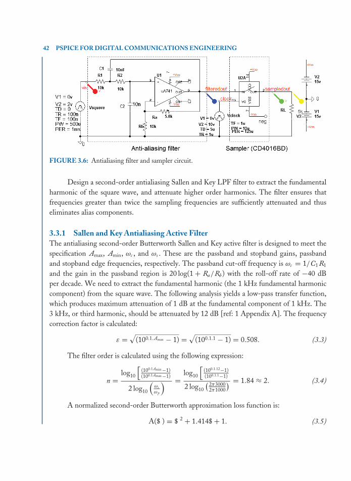
book Mobk066 March 15, 2007 21:18
42 PSPICE FOR DIGITAL COMMUNICATIONS ENGINEERING
FIGURE 3.6: Antialiasing filter and sampler circuit.
Design a second-order antialiasing Sallen and Key LPF filter to extract the fundamentalharmonic of the square wave, and attenuate higher order harmonics. The filter ensures thatfrequencies greater than twice the sampling frequencies are sufficiently attenuated and thuseliminates alias components.
3.3.1 Sallen and Key Antialiasing Active FilterThe antialiasing second-order Butterworth Sallen and Key active filter is designed to meet thespecification Amax, Amin, ωc , and ωs . These are the passband and stopband gains, passbandand stopband edge frequencies, respectively. The passband cut-off frequency is ωc = 1/C1 R1
and the gain in the passband region is 20 log(1 + Ra/Rb) with the roll-off rate of −40 dBper decade. We need to extract the fundamental harmonic (the 1 kHz fundamental harmoniccomponent) from the square wave. The following analysis yields a low-pass transfer function,which produces maximum attenuation of 1 dB at the fundamental component of 1 kHz. The3 kHz, or third harmonic, should be attenuated by 12 dB [ref: 1 Appendix A]. The frequencycorrection factor is calculated:
ε =√
(100.1.Amax − 1) =√
(100.1.1 − 1) = 0.508. (3.3)
The filter order is calculated using the following expression:
n =log10
[(100.1Amin −1)(100.1Amax −1)
2 log10
(ωsωp
) =log10
[(100.1.12−1)(100.1.1−1)
2 log10
( 2π30002π1000
) = 1.84 ≈ 2. (3.4)
A normalized second-order Butterworth approximation loss function is:
A($ ) = $ 2 + 1.414$ + 1. (3.5)

book Mobk066 March 15, 2007 21:18
SAMPLING AND PULSE CODE MODULATION 43
This function has a normalized cut-off frequency of 1 r/s, that is denormalized byreplacing $ with
$ = sε1/n
ωc= s
0.5081/2
2π1000= s
0.7126283
. (3.6)
Substitute this value into (3.5) and invert to yield the transfer function:
H($)∣∣$=s 0.712
6283= H(s ) = 1
(s 0.7126283 )2 + 1.414(s 0.712
6283 ) + 1)x
(6283/0.712)2
(6283/0.712)2
= 7.787.107
s 2 + 1.247.104s + 7.787.107. (3.7)
We are now in a position to obtain component values by comparing the denominatortransfer function coefficients of (3.7) to the standard second-order transfer function denomi-nator s 2 + ωp/Q + ω2
p and the transfer function is
E0
Ei= k/C2 R2
s 2 + s (3 − k)/C R + 1/C2 R2. (3.8)
Consider the non-s coefficient term
ω2p = 7.787 × 107 = 1
(C R)2⇒ ωp = 8824.4 = 1
C R. (3.9)
The capacitance is calculated for R = 100 k� as
C = 18824.4 × 105
= 1.139 nF. (3.10)
Compare the s coefficient terms in the denominator of (3.8) and (3.7), and substitute thevalues for C and R:
ωp
Q= 3 − k
C R= 1.247 × 10⁴ ⇒ 3 − k = 1.247 × 104 × 1.139 × 10−9 × 105 = 1.42. (3.11)
The passband gain is
k = 3 − 1.42 = 1.58 = 1 + Ra/Rb ⇒ Ra/Rb = 0.58or Ra = 0.58Rb . (3.12)
If Rb = 10 k�, then Ra = 5.8 k� and a gain of 1.58. Set Output File Options/Printvalues in the output file to 1 ms, Run to time to 10 ms, Maximum step size = 10 u, and pressthe F11 key to simulate. The frequency spectrum for a 1 kHz square wave input signal andother signals are shown in Fig. 3.7.

book Mobk066 March 15, 2007 21:18
44 PSPICE FOR DIGITAL COMMUNICATIONS ENGINEERING
FIGURE 3.7: A 1 kHz square wave spectrum.
FIGURE 3.8: Input speech file.
3.3.2 Speech SignalsA speech signal is applied using the VPWL F RE FOREVER generator as shown in Fig. 3.8.
This generator reads in a speech file “speech.txt,” created and stored on the hard drive inthe “signalsources” directory. Sampling uses the Sbreak switch part operated by a DigClockpart. Set Output File Options/Print values in the output file to 0.1s, Run to time to 1s, andMaximum step size = 100 u and press the F11 key to simulate. Fig. 3.9 shows the input and

book Mobk066 March 15, 2007 21:18
SAMPLING AND PULSE CODE MODULATION 45
FIGURE 3.9: Speech waveforms.
output speech signals in the time domain, but to see the effect of filtering we need to look atthe signals in the frequency domain. Note how the sampled speech sidebands are now locatedat the sampling frequency, and at multiples of the sampling frequency. The reduced frequencyrange is evident from the middle trace, which means that the aliasing components are reducedto such a small value that effectively, they are zero.
3.3.3 Sample and HoldThe schematic in Fig. 3.10 investigates how a signal sample is held at a certain level in betweensampling times. An ideal opamp part is used instead of a ua741 operational amplifier in order
FIGURE 3.10: Sampler with reconstruction filter.

book Mobk066 March 15, 2007 21:18
46 PSPICE FOR DIGITAL COMMUNICATIONS ENGINEERING
to satisfy the evaluation version limits. Set Output File Options/Print values in the outputfile to 100 ns, Run to time to 10 ms, and Maximum step size = 10 u and press the F11 key tosimulate and observe, in the right pane of Figure 3.13, the effect of not buffering the sampleand hold circuit components.
A square wave signal has a spectrum that extends to infinity and may be used to simulatecomplex signals such as speech. The sampling frequency in modern telecommunication systemsis 8 kHz, which is a sampling period of T = 125 µs. This means that the maximum frequency ofthe input signal should not be greater than 4 kHz. This is achieved by band-limiting the inputanalog signal to 4 kHz using an active low-pass filter. The antialiasing filter specification definesAmax, Amin, ωc , and ωs as the passband gain, stopband gain, the passband edge frequency, andthe stopband edge frequency, respectively. The passband cut-off frequency is ωc = 1/C1 R andthe passband gain is 20 log(1 + Ra/Rb). We may investigate aliasing by reducing the samplingrate below the minimum rate required, which for a 3.4 kHz modulating signal is 6.8 kHz andlower.
The undersampled signal spectrum is compared to the correct sample spectrum. Un-dersampling the input signal will produce aliasing components in the recovered spectrum andcontains extra aliasing frequency components. This manifests itself as distortion in the recov-ered signal. Increase the sampling rate to 20 kHz and observe any changes in the recoveredsignal. Oversampling reduces the “burden” on the antialiasing filter and thus a simpler filterdesign would suffice. In the sample and hold circuit, the hold capacitor, Ch , across the holdresistance, Rh , “holds” the instantaneous amplitude of the sampled signal over the samplingperiod until the next sample and thus produces less distortion in the recovered signal. Wemay observe the effect of not using a hold circuit by observing the frequency spectrum andmeasuring the distortion. Sample and hold may introduce aperture error, however, dependingon how much the signal changes during the period of sampling. We need to calculate the slopeof the 1 kHz sinusoidal signal and multiply it by the sampling period, Ts = 125 us, to calculatethe maximum amount of error introduced. Consider the instantaneous value of a sinusoidal tobe sampled:
νc (t) = Vc sin ωt = 1 sin 2π103t V. (3.13)
We determine the maximum voltage error from the maximum rate of change, or slope,which occurs at the zero crossover point for the sine wave shown in Fig. 3.11. Differentiating(3.13) yields
dνc (t)dt
= ωVc cos ωt = 2π f cos ωt = Vc
t. (3.14)

book Mobk066 March 15, 2007 21:18
SAMPLING AND PULSE CODE MODULATION 47
FIGURE 3.11: Maximum slope occurs at the zero crossover point.
The maximum slope occurs at time t = 0 s:
dνc (t)dt
∣∣∣∣t=0
= ωVc = 2π f Vc = Vc
t⇒ Vc = 2π f Vc t. (3.15)
Thus, the maximum voltage error is Vc = 2π f Vc t, where
2t = Tclock = 1fclock
⇒ t = 12 fclock
= 12 × 8000 × 103
= 62.5 × 10⁻⁶ s. (3.16)
Substituting this value into (3.15) yields the maximum voltage error as
Vc = 2π × 103 62.5 × 10−6 = 392 × 10−3 V. (3.17)
Draw the sample and hold schematic shown in Fig. 3.12. A reconstruction filter isincluded and has the same cut-off frequency as the input LPF in the sampler circuit consideredpreviously.
The recovered signals in the right panel in Fig. 3.13 show the effect of not buffering thehold circuit.
The sample and hold pulse is the weighted inverted delayed unit step subtracted from aunit step also weighted by V :
h(t) = V u(t) − V u(t − Ts ). (3.18)

book Mobk066 March 15, 2007 21:18
48 PSPICE FOR DIGITAL COMMUNICATIONS ENGINEERING
FIGURE 3.12: Sample and hold and recovery schematic.
FIGURE 3.13: Sample and hold time signals.
From the inverse Laplace Transform tables, we get an expression in time for the signalsin the charging period:
F(s ) =t∫
0
V e−s td t =[−V
se−s t
]t
0= −V
s
[e−t − e−0] = V
s[1 − e−t]. (3.19)
The sampling and hold signals are shown in Fig. 3.14 but note the charging and dis-charging periods.
A correct choice for the hold circuit components must be chosen; otherwise we getdistortion in the final output signal.
Administrator
Sticky Note
Correct the integrated signal e−st
paul
Pencil
paul
Pencil
paul
Pencil
paul
Pencil
paul
Pencil
paul
Pencil
paul
Pencil

book Mobk066 March 15, 2007 21:18
SAMPLING AND PULSE CODE MODULATION 49
FIGURE 3.14: Magnified sample and hold signals.
3.4 QUANTIZATION NOISEQuantization noise, q , is an unwanted product produced in the conversion from analog signalsinto a digital format. Analog to digital converters (ADC) produce this noise and it is reducedby increasing the number of levels, M, in the ADC process. The signal to noise ratio (SNR)in analog circuits is defined as the ratio of the signal amplitude to the noise amplitude present.In sampled systems, however, the signal to quantization noise ratio (SQNR) is the ratio ofsignal power to quantizing noise power. The easiest way to examine SQNR is to apply asinusoidal signal V cos ωt that occupies the full range of the quantizer. The full-scale value isVFS = 2nq/2, where n is the number of bits used. The average signal power for full-scale voltageVFS is
Pmax = Vrms
R= (VFS/
√2)2
R= (q M/
√2)2
R= q 2(2n/2
√2)2
R= q 222n
8R. (3.20)
The quantizing noise voltage is limited to ± q /2 and, except at the signal peak level,the voltage has all values within this range occurring with equal probability. The averagednormalized noise power is determined by integrating the quantization noise voltage (saw-toothed in shape and with a negative slope −q t/T0 over a period T0):
Nq = 1T0
∫ T0/2
−T0/2
[− q
T0t]2
dt = q 2
3T30
[T3
0
8+ T3
0
8
]= q 2
12. (3.21)

book Mobk066 March 15, 2007 21:18
50 PSPICE FOR DIGITAL COMMUNICATIONS ENGINEERING
The ratio of the signal power to noise power SQNR for a signal that occupies the fullscale is
SNQR = 10 log10Pmax
PN= 10 log10
[22nq 2/8q 2/12
]= 10 log10
[32
22n]
= 10 log10
[32
M2]
(3.22)
SNQR = 10 log10 22n + 10 log10 1.5 = 20n log10 2 + 10 log10 1.5 = 6.02n + 1.77 dB.
(3.23)However, the SQNR decreases when the input sinusoid is below the full scale of the
ADC. Signal power is a function of waveform shape but noise power is independent of thesignal shape. The signal power for a sinusoid with amplitude ±A is A2/2 and A2 for a squarewave and A2/3 for a triangular wave.
3.5 ANALOG TO DIGITAL CONVERSIONAn 8-bit analog to digital converter (ADC) and digital to analog conversion (DAC) is shown inFig. 3.15. The low-pass filter on the output reconstructs the original input signal. To measurethe quantization noise we use a notch filter to remove the desired signal leaving the quantizationnoise. The 8-bit ADC binary output, set to the nearest integer, in given by
Vin
Vref2nbits. (3.24)
The digital to analog converter (DAC) output produces a rough version of the originalinput signal. A low-pass filter attenuates the high-frequency components leaving the originalsignal. Consider the input and reference voltages for an 8-bit system. The VSIN part parametersare as follows: VOFF = 10 V and VAMPL = 10 V, giving a peak input of Vin = 20 V. Weset the reference to 256 V in order to read the output in binary directly. The binary equivalentfor the ADC reference voltage, VREF, is equal to 256 V and is (20 × 28/256) equal to 10100.From the PROBE plot read the most significant bit to the least significant as b4 b3 b2 b1 b0.
FIGURE 3.15: PCM coder and decoder system.

book Mobk066 March 15, 2007 21:18
SAMPLING AND PULSE CODE MODULATION 51
FIGURE 3.16: 20 V input voltage.
The signal in Fig. 3.16 shows the input 10 V offset raising the 10 V AC input. The binarysignal is read vertically downward using the cursor located at the maximum input signal of20 V.
3.5.1 DAC ResolutionThe DAC output is calculated as
Vout = Vref
[D72
+ D64
+ D58
+ D416
+ D332
+ D264
+ D1128
+ D0256
]V . (3.25)
The output voltage for a binary DAC output 00001001 and 256 V reference voltage is
Vout = Vref
[02
+ 04
+ 08
+ 016
+ 132
+ 064
+ 0128
+ 1256
]= 256(1/32 + 1/256) = 9 V .
(3.26)The DigClock conversion clock has on/off times equal to 20 µs. Set the transient
parameters as follows: Output File Options/Print values in the output file = 1ms, Run totime = 20ms, Start saving data after = 2ms. Making the Output File Options/Print valuesin the output file larger than the 20 ns default value will speed up the simulation time in mostinstances. However, it must be set to a value smaller than the Run to time. If all eight bitsare used, i.e., full scale, then we will have 256 levels available (28 = 256). Table 3.1 shows therelationships between the ADC resolution and the voltage reference Vref.

book Mobk066 March 15, 2007 21:18
52 PSPICE FOR DIGITAL COMMUNICATIONS ENGINEERING
TABLE 3.1: The ADC and Reference Relationship
VIN (V) VREF (V) NO. OF BITS NO. OF LEVELS RESOLUTION (V)
9 16 8 28 = 256 0.0625
9 32 7 27 = 128 0.125 V
9 64 6 26 = 64 0.25
9 128 5 25 = 32 0.5
9 256 4 24 = 16 1
The input signal VSIN generator parameters are VOFF = 5 V, VAMPL = 4 V, andFREQUENCY = 1 kHz. To measure the quantization noise, we must attenuate the 1 kHzinput signal using a band-stop notch filter.
3.5.2 Band-Stop FilterThe band-stop (notch) filter is implemented using an ABM part called BANDREJ. The filter ischaracterized by six parameters: four cut-off frequencies and two attenuation values—RIPPLEdefines the maximum allowable ripple in the passband and STOP is the minimum attenuationin the stopband. Set the Analysis tab to Analysis type: AC Sweep/Noise, AC Sweep Type toLinear/Logarithmic, Start Frequency = 100, End Frequency = 10 k, Total Points/Decade= 10001. Enter the lowest frequency F0 to highest frequency F3 for the band-stop filterparameters as shown in Fig. 3.17. A value for either of the passband frequencies, say f p1(orstop frequencies), is calculated by assuming a value for one of the passband frequencies andknowing the center frequency to yield for f p2
f0 =√
( fs 1 fs 2) =√
( f p1 f p2) ⇒ f p2 = f 20 / f p1. (3.27)
FIGURE 3.17: The band-stop part called BANDREJ.
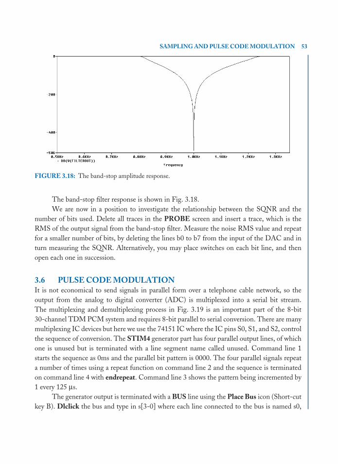
book Mobk066 March 15, 2007 21:18
SAMPLING AND PULSE CODE MODULATION 53
FIGURE 3.18: The band-stop amplitude response.
The band-stop filter response is shown in Fig. 3.18.We are now in a position to investigate the relationship between the SQNR and the
number of bits used. Delete all traces in the PROBE screen and insert a trace, which is theRMS of the output signal from the band-stop filter. Measure the noise RMS value and repeatfor a smaller number of bits, by deleting the lines b0 to b7 from the input of the DAC and inturn measuring the SQNR. Alternatively, you may place switches on each bit line, and thenopen each one in succession.
3.6 PULSE CODE MODULATIONIt is not economical to send signals in parallel form over a telephone cable network, so theoutput from the analog to digital converter (ADC) is multiplexed into a serial bit stream.The multiplexing and demultiplexing process in Fig. 3.19 is an important part of the 8-bit30-channel TDM PCM system and requires 8-bit parallel to serial conversion. There are manymultiplexing IC devices but here we use the 74151 IC where the IC pins S0, S1, and S2, controlthe sequence of conversion. The STIM4 generator part has four parallel output lines, of whichone is unused but is terminated with a line segment name called unused. Command line 1starts the sequence as 0ms and the parallel bit pattern is 0000. The four parallel signals repeata number of times using a repeat function on command line 2 and the sequence is terminatedon command line 4 with endrepeat. Command line 3 shows the pattern being incremented by1 every 125 µs.
The generator output is terminated with a BUS line using the Place Bus icon (Short-cutkey B). Dlclick the bus and type in s[3-0] where each line connected to the bus is named s0,

book Mobk066 March 15, 2007 21:18
54 PSPICE FOR DIGITAL COMMUNICATIONS ENGINEERING
FIGURE 3.19: Multiplexing and demultiplexing.
s1, s2, and s3. Placing a marker on a bus produces a PROBE display in hexadecimal format.The clock frequency is twice the speed of the STIM4 part increment (i.e. half the time period).In an actual system, the final output s3 could synchronize the system. The serial data is appliedusing a STIM1 part.
Set the Analysis tab to Analysis type: Time Domain (Transient), Run to time = 10ms,and Maximum step size = (left blank), Press F11 to simulate. The waveforms for the mux–demux devices are shown in Fig. 3.20.
3.6.1 Universal Shift Register74194 LS is a 4-bit bidirectional universal shift register where all data and mode control inputsare edge-triggered and respond to LOW to HIGH clock transitions only. The mode control
FIGURE 3.20: Serial to parallel and parallel to serial conversion.

book Mobk066 March 15, 2007 21:18
SAMPLING AND PULSE CODE MODULATION 55
TABLE 3.2: 74194 Universal Shift Register
OPERATING CLR S1 S0 SR SL PN QA QB QC QDMODE (1) (10) (9) (2) (7) (3–6) (15) (14) (13) (12)
Reset L X X X X X L L L L
Hold H L L X X X Q0 Q1 Q2 Q3
Shift left H H L X L X Q1 Q2 Q3 L
H H L X H X Q1 Q2 Q3 H
Shift right H L H L X X L Q0 Q1 Q2
H L H H X X H Q0 Q1 Q2
Parallel load H H H X X Pn P0 P1 P2 P3
and selected data inputs must be stable one setup time prior to the positive transition of theclock pulse. The four parallel data inputs, P0, P1, P2, P3, are D-type inputs (also called A, B,C, and D). When both S0 and S1 are HIGH, signals presented to P0, P1, P2, and P3 inputs aretransferred to Q0, Q1, Q2, and Q3 outputs, respectively, following the next LOW to HIGHtransition of the clock. This is a parallel-to-parallel conversion. The mode control inputs, S0and S1, determine the synchronous operation of the device. Table 3.2 shows how data is shiftedfrom left to right (Q0 → Q1), or right to left (Q3 → Q2). Parallel data is entered, by loadingall four bits of the register simultaneously.
When both S0 and S1 are LOW, the existing data is retained in a “do-nothing” modewithout restricting the HIGH to LOW clock transition. D-type serial data inputs (SR, SL)allow multistage shift right or shift left data transfers without interfering with parallel loadoperation, and will appear on the QA and QC outputs. The asynchronous clear (CLR), whenLOW, overrides all other input conditions and forces the Q outputs LOW.
In the table, L = low level, H = high level, X = do not care, l = LOW voltage level onesetup time prior to the LOW to HIGH clock transition; h = high voltage level one setup timeprior to the LOW to HIGH clock transition; P(n) and Q(n), where n indicates the state of theinput or output one setup time prior to the LOW to HIGH clock transition.
3.6.2 74194 Universal Shift RegisterDraw the schematic in Fig. 3.21. What is the output for the parallel input 0110? Set the Analysistab to Analysis type: Time Domain (Transient), Run to time = 10ms, and Maximum stepsize = (left blank), press F11 to simulate.

book Mobk066 March 15, 2007 21:18
56
FIGURE 3.21: Universal shift register.
FIGURE 3.22: Universal shift register signals.
3.7 SINGLE-CHANNEL 4-BIT PCM TRANSMITTERThe simple PCM system in Fig. 3.23 uses only four of the 8 bits available, but it may beextended to an 8-bit capability using additional IC circuitry (see exercise at the end of thechapter). Here, we apply a 1 kHz sinusoidal signal and sample it at 8000 Hz, which is therate used in the public switched telephone network (PSTN) and converts the ADC paralleloutput to a serial bit stream. To test that the circuit is working correctly, we need to reverse theprocedure and attach a serial to parallel converter, a latch for temporary store, and a DAC.
The DAC output is then low-pass filtered. The registers must be initialized to a certainstate. Select the Simulation Setting menu and then select the Options tab. In the Categorybox select Gate-Level Simulation. This will then show the Timing Mode - select Typical. Inthe Timing Mode change Digital Setup from Typical to Maximum. The Initialize all flipflops is set to All 1. Failing to do this will result in the flip-flop being in an undeterminedstate, i.e., All X, and shows up in the plot as two red lines. Set the Analysis tab to Analysistype: Time Domain (Transient), Run to time = 2ms, and Maximum step size = (left blank),Press F11 to simulate.

book Mobk066 March 15, 2007 21:18
SAMPLING AND PULSE CODE MODULATION 57
FIG
UR
E3.
23:
Sing
le-c
hann
el4-
bitP
CM
tran
smitt
eran
dre
ceiv
er.

book Mobk066 March 15, 2007 21:18
58 PSPICE FOR DIGITAL COMMUNICATIONS ENGINEERING
FIGURE 3.24: Input and recovered signals.
The recovered 1 kHz sinusoid in Fig. 3.24 has distortion that is displayed using the FFTfunction.
The timing waveforms should be investigated.
3.8 TIME-DIVISION MULTIPLEXING AND DEMULTIPLEXINGIn the European E1 PCM telephone systems, 30 voice signals are sampled, coded, and mul-tiplexed, to produce a 2.048 Mb/s digital signal that is transmitted over a high-bandwidthline, coaxial cable, microwave line-of-sight link, optical fiber, etc. Sample binary values aremultiplexed using byte interleaving so every 125 µs a framing bit is followed by a coded samplefor each of the 30 voice signals. Other housekeeping bits are allocated for different purposes.Also super frames take care of the signaling requirements by 16 frames with the center timeslot used for two channel signaling of 4 bits each. The transmission rate is 257 bits every 125 µs(2.048 Mb/s = 8000 × 8 × 32). The U.S. and Japanese 24-channel time-division multiplexed(TDM) PCM system generates a composite bit stream for a total of 24 digitized voice channelsand results in a frame structure consisting of 193 bits in each 125 µs time interval. Secondarymultiplexed systems combine primary multiplexing digital streams into a higher rate outputbit stream called the plesiochronous digital hierarchical structure. A TDM transmitter andreceiver, using ABM library parts, are shown in Fig. 3.25. Set the Analysis tab to Analysis type:Time Domain (Transient), Run to time = 4ms, and Maximum step size = (left blank), PressF11 to simulate.
Fig. 3.26 shows the TDM and recovered signals.
3.8.1 Time-division Multiplexing of Two PAM SignalsThe 4066 IC in Fig. 3.27 multiplexes two signals. One of the electronic switches may be used(see exercise 12 at the end of the chapter) to invert the clock so that the second signal is sampledwith a delay of one clock period.