Psec timing/LAPPD program at Chicagofrisch/talks/CPAD_Oct13_2017_v4.pdf · Topics 10/12/2017O CPAD...
37
Psec timing/LAPPD program at Chicago 10/12/2017O 1 Evan Angelico, Andrey Elagin, HJF, Rich Northrop, Carla Pilcher, Eric Spieglan plus Eric Oberla (emeritus) and Mircea Bogdan on electronics plus 12 (!) HS and undergrad students last summer
-
Upload
nguyenkhuong -
Category
Documents
-
view
215 -
download
0
Transcript of Psec timing/LAPPD program at Chicagofrisch/talks/CPAD_Oct13_2017_v4.pdf · Topics 10/12/2017O CPAD...

Psec timing/LAPPD program at Chicago
10/12/2017O 1
Evan Angelico, Andrey Elagin, HJF, Rich Northrop, Carla Pilcher, Eric Spieglan plus Eric Oberla (emeritus) and Mircea Bogdan on electronics
plus 12 (!) HS and undergrad students last summer

Our (UC) LAPPDTM ‘Tile’
2
1. 8” x 8” active area (MCP size) 2. Amplification: a pair of MgO MCPs in a chevron config. 3. Measured gain typically 107
4. Space resolution 700 microns in 2D (strips); 300 microns with ½” pads if signals are shared
5. Time resolution: < 50 psec single photon measured, goal of a < a few (or one) for charged particles traversing window (50 PE) or high energy photons (i.e. large pulses)
B.W. Adams, A. Elagin, H. Frisch, R. Obaid,E. Oberla, A. Vostrikov, R. Wagner, J. Wang, M. Wetstein;{\it Timing Characteristics of Large Area Picosecond Photodetectors};Nucl. Inst. Meth. Phys. Res. A. , Vol. 795, pp 1-11 (Sept. 2015);

Topics
10/12/2017O CPAD Albuquerque 2017 3
1. Photodetector development (R&D with Incom Inc) a) Indium window-to-tilebase seal b) Application-independent anode (pads or strips)– metal
resistive capacitive coupling c) Ceramic robust high-bandwidth 1-piece body d) PMT-process batch production: facilities, process e) Theory-based photocathodes (with RMD, Smedley,
Attenkofer)
2. Electronics (Eric Oberla, Mircea Bogdan, ANNIE) a) Multibuffer 130nm CMOS 10 GS/sec ASIC developmnt b) Scalable FPGA-based DAQ readout/control for ANNIE
3. Goals- expand physics reach via psec timing frontier: testbeam and simulation studies (PhD students, Elagin): a) Optical Time Project Chamber for double-beta decay b) Collider photon/ch vertexing and track quark content

Recent papers (see lappddocs.uchicago.edu)
• E. Angelico, T. Seiss, B. W, Adams, A. Elagin, H. J. Frisch, E. Spieglan;\\{\it Capacitively coupled pickup in MCP-based photo-detectors using a conductive, metallic anode};\\Nucl. Inst. Meth. Phys. Res. A. (Oct. 2016)
• A. Elagin, H. J. Frisch, B. Naranjo, J. Ouellet, L. Winslow, T. Wongjirad;\\{\it Separating Double-Beta Decay Events from Solar NeutrinoInteractions in a Kiloton-Scale Liquid Scintillator Detector By Fast Timing};Nucl. Inst. Meth. Phys. Res. A. (Sept. 2016)
• E. Oberla and H.J. Frisch;\\ {\it Charged particle tracking in a water Cherenkov optical time-projection chamber};\\ Nucl. Inst. Meth. Phys. Res. A. Volume 814, 19-32, (April 2016)% ISSN 0168-9002. arXiv:1510.00947
10/12/2017 CPAD Albuquerque 2017 4
Andrey and Evan will give talks at Light 2017 next week on tile production and OTPC.

5
1: TOP SEAL: glass sidewall to window- consider proven
Recipe (lots of characterization, vendor/Ossy input) 1. Very clean glass surfaces 2. 200 nm of Nichrome 3. 200 nm of Cu w no vacuum break 4. .9999 Indium wire sized for volume 5. Etch Indium wire in 5% HCl 6. Thermal cycle 100C above melting 7. Press down on window edges w DOF
What happens: (Andrey Elagin FIB/SEM/ studies) (ITT story) 1. Nichrome layer will provide tie layer 2. Cu provides protection against oxide on NiCr 3. Indium wire gets squished--oxide broken (Walters) 4. Cu diffuses into bulk Indium (Ossy said so) 5. Nickel and Chrome diffuse into bulk Indium (!) 6. A very thin layer containing chrome on the glass
forms the bond to the indium.
Photodetector Development

The LAPPD size introduces 3 serious problems not experienced in making smaller tubes:
1. Uniform metalization, indium distribution, and cleanliness over a much longer length (~36”)
2. Uniform pressure and heating over that length 3. In a transfer process base sealing surface level to a
mil or less (?-number I don’t know, as we use wire captured in place between the window and sidewall)
6
TOP SEAL- continued Photodetector Development
And, a precise STACK HEIGHT over entire tile.
1. FEA and many trials dictate a stack height low by 0.0020.0005” over the tile interior
2. Each button spacer has to be custom shimmed to meet the above
3. Pressing uniformly on the edges over the seal area on all 4 sides is essential
Note buttons make stack height a discrete problem

7
Photodetector Development
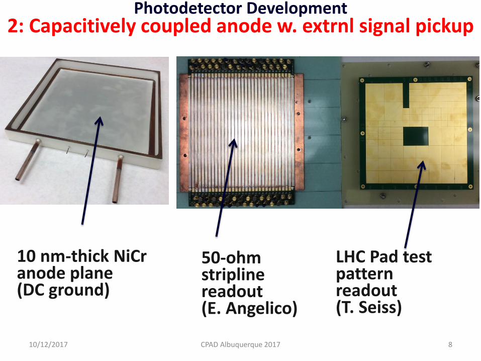
2: Capacitively coupled anode w. external signal pickup
10/12/2017 CPAD Albuquerque 2017
1. Metal layer rather than thick-film for production during seal layer coating (also realities of thick-film)
2. 10nm of NiCr is resistive enough for RC (capacitive) coupling
8
2: Capacitively coupled anode w. extrnl signal pickup
10/12/2017 CPAD Albuquerque 2017
10 nm-thick NiCr anode plane (DC ground)
50-ohm stripline readout (E. Angelico)
LHC Pad test pattern readout (T. Seiss)
Photodetector Development

9 10/12/2017 CPAD Albuquerque 2017
Comparison of risetimes direct vs capacitively coupled on strip readout PC-card
Comparison of risetimes direct vs capacitively coupled on pad readout PC-card
Photodetector Development Capacitively coupled anode w. extrnl signal pickup

10 10/12/2017 CPAD Albuquerque 2017
Sharing of the signal across two adjacent ½” pads
Position resolution with ½” pads and large signals (256 pads per LAPPD).
Advantage for Incom in they make 1-design tube; user defines readout pattern, resolution, band-width on card
Photodetector Development

11
3: Ceramic robust high-bandwidth 1-piece tile base
1. Our university group complement s Incom’s commercial focus on production of their glass tile design in 2 ways: 1. Develop physics applications (e.g. OTPC; later in talk) 2. Evolutionary design options- (but don’t get in their
way on the Gen-I glass tile while working on Gen-II!)
2. Have developed a `Green-trimmed’ ceramic tile base with the following advantages: 1. One piece- no assembly of sidewall and base w. frit 2. Hotter bake-out possible as no frit or silver ink anode 3. Higher bandwidth than glass (also no ion migration) 4. More robust than glass 5. Working closely with Mike Foley of Incom under a
DOE Nuclear Physics SBIR Disadvantages: long lead-times, no experience (vs glass)
Photodetector Development

12
3: Ceramic robust high-bandwidth 1-piece tile base
Sidewall and anode plane are green-trimmed and then ground to spec after full fire- no fritted or brazed large (long) joint
Ceramic tile bases from 4 vendors- have 5 from each
Photodetector Development

13
3: Ceramic robust high-bandwidth 1-piece tile base Multipurpose metallizing (‘coating’) glass or ceramic
1. Major roadblock for both glass and ceramic (surprise!)- source of a lot of delay working out
2. Expert territory only: Eileen Hahn (Fermilab), Sharon Jelinsky (SSL), Bing Xu (ANL), commercial precision optical coaters (2 vendors)
3. Here we use coating for sealing surfaces, capacitively-coupled anode, and connection to pins to interior- single process (no vacuum break between sealing layers)
4. Now have 2 good vendors+
Photodetector Development
200/200 nm NiCr/Cu seal surface
NiCr/Cu anode border
10 nm NiCr anode

14
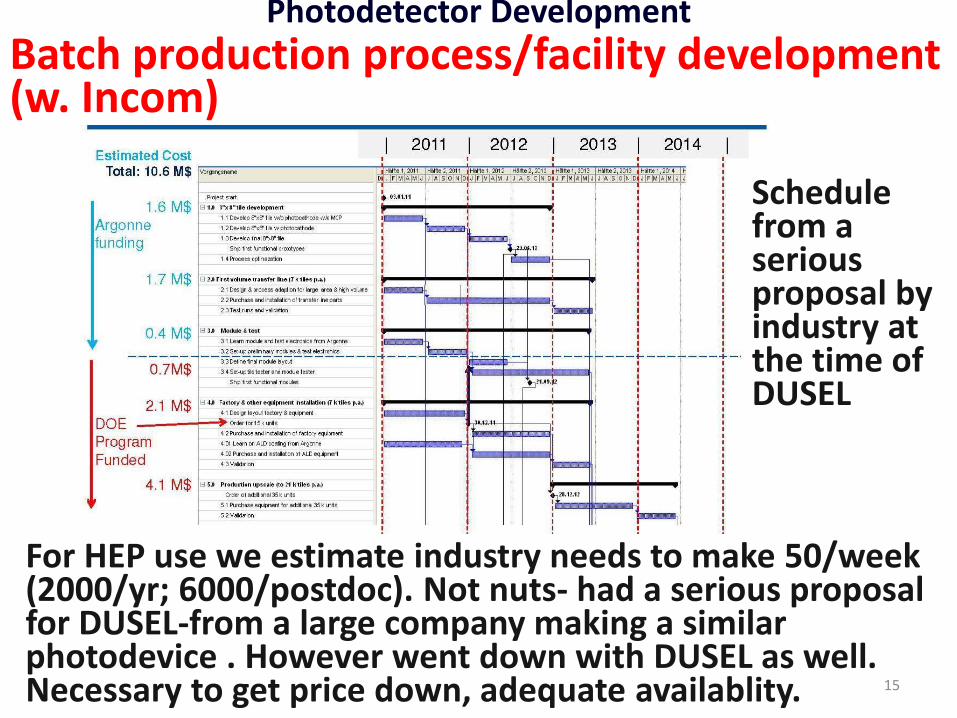
4: Batch production process/facility development (w. Incom) Conventional PMTs are (usually) made in batches, using the hermetic package as the UHV environment
PMT Process Characteristics 1. Many tubes on one pump 2. Very poor external
vacuum- Oring seal on tubulation, small long path to small pump. Internal getter+alkali provide the UHV pumping
3. External oven heating only tube (not vessel)
4. Alkali source internal or external (Brits)
5. Tubes are accessible during photocathod synthesis
Photodetector Development
15
Batch production process/facility development (w. Incom)
For HEP use we estimate industry needs to make 50/week (2000/yr; 6000/postdoc). Not nuts- had a serious proposal for DUSEL-from a large company making a similar photodevice . However went down with DUSEL as well. Necessary to get price down, adequate availablity.
Photodetector Development
Schedule from a serious proposal by industry at the time of DUSEL

10/12/2017 CPAD Albuquerque 2017 16
Photodetector Development Batch production process/scaleable facility development (w. Incom NP SBIR )- replicable
Margherita I
Margherita II (improved)
New lab (!)
Wet lab (!!)

17
5: Theory-based photocathodes (w. RMD, Smedley, Attenkofer ; Luca Cultrera)
Photodetector Development
K2CsSb powder diffraction of RMD cathode material taken at UC
Agenda of 2nd cathode workshop at UC
Collaboration with BNL and RMD, and also Cornell, on `theory-based’ cathodes and workshops led to: a) ties to the cathode community , and the in-situ initiative

18
In-situ photocathode synthesis (Springer, Sinclair) Idea is to emulate RCA/Burle PMT production
Photodetector Development
We have used a `GodParent Committee’ (CDF) to guide us: Klaus Attenkofer (BNL), Luca Cultrera (Cornell), Jeff Elam (ANL), Mike Pellin (ANL), Matt Poelker (JLAB), Charlie Sinclair (Cornell, SLAC), John Smedley (BNL),Gary Varner (Hawaii, Chair)
Steps: 1. Coat (NiCr/Cu) border and electrode fingers on
window 2. Pre-deposit a 10nm Antimony (Sb) layer overlapping
border and fingers 3. Seal window to tile base with a bake-out/sealing
thermal cycle: dual vacuum- 1) tile and 2) vessel 4. Bring vessel to air, leaving sealed tile on its pump 5. Introduce alkali vapor through tubulation while
measuring QE of (exposed) window and resistance of MCP plates and stack
6. Pinch off tubulation when photocathode is done

10/12/2017 CPAD Albuquerque 2017 19
Photodetector Development
In-situ photocathode synthesis (Springer, Sinclair)
• GPs recommended doing only Cs first • Expect uniformity to be determined by thickness of Sb
layer- should very uniform

20
Photodetector Development
In-situ photocathode synthesis (Springer, Sinclair) Successes • We have learned how to manipulatethe movement of Cs
around inside the system (remember we’re beginners) • Vapor reached everywhere on the window- uniform • Chemical reaction between Cs and Sb seems to be `self-
limiting’ as expected- reaches a defined end-point • QE seems to be consistent with reasonable Cs3Sb
cathode, but we cannot measure it precisely yet (subtlety I missed completely- can explain if asked in questions)
• MCP plates are not permanently damaged/changed Problems discovered: • MCP plates go to lower resistance (recoverable in air) • We had exposed Cu on the window- Indium wet it. Cs
interacts with Indium to form a black powder. • Resistive buttons interact with Cs (new buttons
yesterday) • Measuring QE is made more difficult by our internal HV
divider (can’t get current across first gap directly).

In-Situ Cathode Synthesis Trials in Progress
21
Evan (FIB/SEM) and Andrey (SEM)
E.g. The black powder from cesiating excess indium Sealing surface on top of sidewall
Black powder NiCr anode
(New windows will have no exposed Cu- few weeks away)
Analysis showing it’s a CsIn compound

Electronics
10/12/2017 CPAD Albuquerque 2017 22
Eric Oberla’s Ph.D thesis; Mircea Bogdan, John Podczerwinski, Horatio Li, Evan Angelico; John Porter of Sandia funded PSEC4A Mosis run; Jonathan Eisch, Miles Lucas,, .. (ANNIE)
Now 64 bds (1920 channels)
Now +SFP and VME
We (Porter, Sandia) have the new PSEC4A ASIC
Now +SFP and VME
We have a new Central Card- Mircea Bogdan

The Original Motivation: I GotTired of @#$! Jets Goals: 1) Measure all 4-vectors– can reconstruct masses 2) assign tracks to vertices (e.g. CMS forward Ecal.) 3) vertex photons at colliders (4-vectors!) ;
See Aspen talk, Jan 2003 (hep.uchicago.edu/~frisch 23
CDF top quark event
10/12/2017
Aside: Use photons (and electrons) as reference time- i.e. do differential timing of tracks from the same vertex to eliminate external clock jitter

Three Timing Cases to Distinguish
10/12/2017 24
1. Single optical photons (Scintillation or Cherenkov) 2. Charged Particles above Cherenkov Threshold(H2O,glass) 3. Electromagnetic showers from High Energy photons
The factors limiting the ultimate timing resolution are different in each of the following cases:
I will focus on #2 and #3, relativistic charged particles and high energy photons, for which psec or sub-psec time resolutions I believe are plausible given certain detection criteria are met.
Note: In what follows I treat time and space distances in the same units, i.e. c=1, and 1 psec =300 microns; 1 nsec =1000 psec; 1 nsec =1 foot

Criteria for Sub-Psec Timing-1
10/12/2017O 25
Fast Source: A psec source in time-space of many photons in a time-space interval (example: Cherenkov light from a charged particle traversing a radiator or the entrance window of a photodetector ); e, mu, pi, K, p,…
( Or early in an electromagnetic shower such as in a pre-radiator or EM calorimeter ( separate discussion));
Cherenkov photons

Criteria for Sub-Psec Timing-2
10/12/2017O 26
Psec-level pixel size (example: 10-20 micron pores in an MCP plate)
e, mu, pi, K, p,…
10-20 micron pore

Criteria for Sub-Psec Timing-3
10/12/2017O 27
High gain: The gain has to be high enough that a single photon triggers, i.e. the first photon ‘in’ determines the leading edge of the pulse and consequently the timing.
e, mu, pi, K, p,…
Amplification section: Gain-bandwidth, Signal-to-Noise, Power, Cost (eg: two-stages of MgO MCPs give gain >107)
N.B. NOT 1/sqrt(N)

Signal-to-Noise, Rise-time Dependences
10/12/2017 28
Long discussions at UC/ANL /France workshops of dependence on analog bandwidth, gain, noise, digitization methods, etc. ; Answer (S. Ritt) is that at the level of present performance, using waveform sampling, the achievable time resolution is well-described by three parameters: 1) analog band-width (aka rise-time); 2) signal-to-noise; and 3) the sampling rate (assuming sufficient number of bits not to limit).
• Show Stefan Ritt’s Rule-of-Thumb. For a sampling rate
proportional to analog bandwidth it’s only 2 parameters.

Breaking the 1-Psec Barrier?
Stefan Ritt (PSI) table from 2nd Chicago Photocathode Workshop (annotated) (see psec.uchicago/edu/library)
10/12/2017 29
? 0.7 mv 15 GS/sec LAPPD: 1V 1.5 GHz !
Before 100 fsec something else will surely bite us, but still…
Signal Noise Sampling Bandwidth Resolution
??

Present (now old) Time Resolution
10/12/2017 30
Single Photo-electron PSEC4 Waveform sampling
Sigma=44 psec
Differential Time Resolution Large signal Limit
Oscilloscope Readout Black line is y=3.1x+0.5 (ps) Red line is y=2.8x +1.5 (ps)
Where the constant term represents the large S/N limit (0.5-1.5 ps)
Highly non-optimized system (!)- could do much better

Timing res. agrees with MC
Time resolution on 2 ends of 8”-anode strip vs (S/N)-1 in psec (pair of 8” MCP’s)
< 6 psec
M. Wetstein, B. Adams, A. Elagin, R. Obaid, A. Vostrikov, …
Laser spot size
31 10/12/2017

Next round of big collider detectors
• Should measure 4-vectors of all tracks up to (say ) PT= 25 GeV using ultra-fast TOF
• Should vertex all particles using ultra-fast TOF, including photons
• For ultra-fast TOF need small pixels, high gain, and lots of photons in a coherent localized pulse.
10/12/2017 CPAD Albuquerque 2017 32
Opinion, pure and simple (why not)
The End 10/12/2017 33
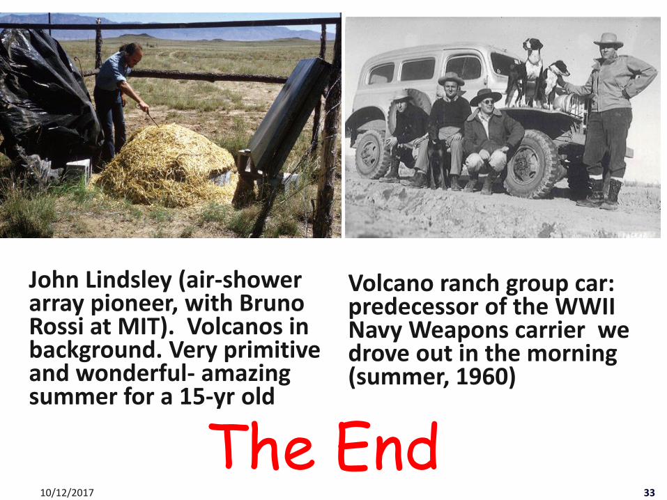
John Lindsley (air-shower array pioneer, with Bruno Rossi at MIT). Volcanos in background. Very primitive and wonderful- amazing summer for a 15-yr old
Volcano ranch group car: predecessor of the WWII Navy Weapons carrier we drove out in the morning (summer, 1960)

Acknowledgements
10/12/2017 34
• H. Marsiske, H. Nicholson and the US DOE Office of Science
• Staff and management at Incom and Arradiance
• Colleagues and collaborators at ANL , SSL, and Hawaii
• Others in the field of fast-timing , with special thanks to T. Ohshima and J. Vavra; and waveform sampling, with special thanks to E. Delagnes, J.F.-Genat, S. Ritt, and G. Varner
This work supported by U. S. Department of Energy, Office of Science, Office of Basic Energy Sciences and Offices of High Energy Physics and Nuclear Physics under contracts DE-SC0008172 and DE-SC0015367; the National Science Foundation under grant PHY-1066014; and the Physical Sciences Division of the University of Chicago.

Backup Slides
TIPP June 5, 2014 10/12/2017 35

37
Photodetector Development
Joe Gregar (master glassblower Argonne) and Andrey
Ceramic tile bases from 4 vendors
Second Margherita for ceramic in our brand-new lab; new wet lab (!)

10/12/2017 CPAD Albuquerque 2017 38
A Plea As money gets tight we naturally pull back from risk and disruptive technologies. However the big gains in our exploratory capabilities have come from new things- often not easy- e.g. the TPC and silicon vertex detectors (I was on a godparent committee that approved Aldo Menzione’s for CDF). We should aim for ‘a portfolio’ of risk’– judiciously and thoughtfully chosen; but we should fight the shutting down either new initiatives or career paths for young physicists interested in new ideas.
(N.B. not a plea for my program per se- much broader and more important to the future of US basic science)