NATSYCO. microscopy Optical microscopy Electron microscopy Scanning probe microscope.
Ultramicroscopy ] (]]]]) ]]]–]]]
Contents lists available at SciVerse ScienceDirect
Ultramicroscopy
0304-39
doi:10.1
n Corr
E-m
Pleasand
journal homepage: www.elsevier.com/locate/ultramic
Prospects for electron microscopy characterisation of solar cells:Opportunities and challenges
B.G. Mendis a,n, K. Durose b
a Department of Physics, Durham University, South Road, Durham, DH1 3LE, UKb Stephenson Institute for Renewable Energy, Chadwick Building, University of Liverpool, Liverpool L69 7 ZF, UK
a r t i c l e i n f o
Keywords:
Thin-film solar cells
Grain boundary recombination velocity
Optical property measurement
Morphology of excitonic solar cells
91/$ - see front matter & 2011 Elsevier B.V. A
016/j.ultramic.2011.09.010
esponding author.
ail address: [email protected] (B.G. M
e cite this article as: B.G. Mendis, Kchallenges, Ultramicroscopy (2011),
a b s t r a c t
Several electron microscopy techniques available for characterising thin-film solar cells are described,
including recent advances in instrumentation, such as aberration-correction, monochromators, time-
resolved cathodoluminescence and focused ion-beam microscopy. Two generic problems in thin-film
solar cell characterisation, namely electrical activity of grain boundaries and 3D morphology of
excitionic solar cells, are also discussed from the standpoint of electron microscopy. The opportunities
as well as challenges facing application of these techniques to thin-film and excitonic solar cells are
highlighted.
& 2011 Elsevier B.V. All rights reserved.
1. Introduction
Despite its many benefits as a renewable energy source, solarphotovoltaic energy harvesting can only be commercially viable ifthe cost per Watt (at peak performance) is reduced from its currentvalue of �$4/Wp for the bulk silicon modules that account for�85% of the present day market. Whereas thin-film CdTe modulesare presently priced at �$1/Wp – and are beginning to be com-petitive with grid connected power – it remains the case thatfurther increase in performance and decrease in cost are necessaryto generate unsubsidised mass market conditions. In the case ofbulk silicon, the advantages of high performance are countered bythe high cost of purifying the material and the limits to productionultimately imposed by a wafer-based technology. Consequently‘thin-film’ solar cells, that utilise more efficient light absorbingmaterials or novel light capturing mechanisms, are being intenselyresearched. Electron microscopy is vital for characterising themicrostructure/morphology of these thin-film solar cells, as wellas probing the physics governing device efficiency. In this reviewwe focus on applications of electron microscopy to thin-film solarcells that have been partly brought about by recent advances ininstrumentation. In some cases the techniques are yet to be appliedto solar cells, but have been successfully demonstrated on othermaterials systems.
In Section 2 a brief introduction to solar cell operation and thevarious thin-film devices is presented. Here ‘thin-film solar cell’ isbroadly defined as semiconductor thin-film solar cells and we
ll rights reserved.
endis).
. Durose, Prospects for eledoi:10.1016/j.ultramic.2011
have also included organic and dye-sensitised solar cells. Reviewsfor these devices can be found in [1–11]. A general review ofphysical techniques of analysis for thin-film solar cells includingTEM and electron beam induced current measurements in the SEMis given in [145]. In Section 3 recent advances in electron–optic andrelated instrumentation, and their potential applications in solarcell characterisation are discussed. The instrument advancesselected for review are: (i) aberration-corrected scanning transmis-sion electron microscopy (STEM), (ii) monochromated electronenergy loss spectroscopy (EELS), (iii) time-resolved cathodolumi-nescence in a dynamic scanning electron microscope (SEM) and (iv)focused ion-beam (FIB) microscopy. In Section 4 two widelyencountered generic problems, namely electrical activity of grainboundaries in semiconductor thin-film solar cells and 3D morphol-ogy of excitonic solar cells, are discussed in light of electronmicroscopy characterisation. Conclusions are presented in Section 5.
2. Thin-film solar cells
2.1. Basic operating principles
The common feature of the great majority of solar cell devices isthe p–n junction, the band diagram for a homojunction being shownin Fig. 1. Incident light of energy hu greater than the band gap of theabsorber material generates electrons in the conduction band andholes in the valence band. The photocurrent is due to the generationof minority carriers on each side of the junction. Minority carriersmust diffuse towards the depletion region where the built-in electricfield e will inject them across the p–n junction. As an exampleminority carrier electrons photo-generated within the p-region will
ctron microscopy characterisation of solar cells: Opportunities.09.010
Fig. 1. Shematic illustrating the operating principle of a solar cell via the
electronic band structure of the material. An incident photon of energy hu greater
than the band gap generates electrons (solid circles) and holes (open circles).
Minority carriers that diffuse to the depletion region edge are injected across the
p–n junction, which has a built-in electric field e. See text for further details.
Fig. 2. (a) Schematic electronic band structure for a grain boundary region in
isolation and the neighbouring n-type perfect crystals on either side. Ec, EF and Ev
denote the energies of the conduction band, Fermi level and valence band,
respectively. fo is the quasi-neutrality level of the grain boundary. (b) Band
structure diagram for a grain boundary in contact and in equilibrium with the two
perfect crystals. Energy levels below EF are occupied, which results in negative
charge accumulated at the grain boundary plane. The figures are based on [13].
Fig. 3. Schematic thin-film solar cell device structures for (a) amorphous-Si (a-Si)
solar cells, (b) CdTe solar cells, (c) plasmonic solar cells and (d) radial core-shell
nanowire solar cells. TCO in Fig. 3a,b,d refer to transparent conducting oxide. The
‘i-layer’ in Fig. 3a refers to intrinsic layer, where the number of donors and
acceptors are approximately equal. Note that variations in the device structure are
possible.
B.G. Mendis, K. Durose / Ultramicroscopy ] (]]]]) ]]]–]]]2
be injected into the n-region, where they become majority carriers,provided that the electrons are generated within a diffusion lengthaway from the depletion region. Similar reasoning is applicable toholes photo-generated within the n-region. Solar cell efficiency isgoverned by the ability of photons to generate electron-hole pairsand by the successful separation and collection of the carriers.Electron-hole pair generation depends on the photon energy withrespect to the band gap as well as the absorption coefficient (directband gap materials have higher absorption coefficients sincemomentum is conserved during the optical transition). The idealsolar cell material for a single junction device has a band gap of�1.4 eV [12] and a high absorption coefficient. For further detailssee for example [13].
Separation and collection of carriers depends (amongst otherfactors) on the presence of crystal defects. Consider, for example,the effect of grain boundaries, which are common in inorganicsemiconductor thin-film solar cells (Sections 2.2 and 4.1). Thedifferent atomic bonding environment at a grain boundaryintroduces additional energy levels within the band gap, so thatfor an electrically neutral grain boundary all energy levels belowthe quasi-neutrality level fo are occupied (Fig. 2a). At equilibriumhowever, the grain boundary and neighbouring bulk semiconduc-tor must have a common Fermi energy level, so that, for thesituation depicted in Fig. 2a, electrons are transferred from thebulk regions to the grain boundary plane. This results in a
Please cite this article as: B.G. Mendis, K. Durose, Prospects for eleand challenges, Ultramicroscopy (2011), doi:10.1016/j.ultramic.2011
depletion region on either side of the grain boundary, and theresulting upward band bending repels the majority carrier elec-trons (Fig. 2b). Minority carrier holes are attracted towards theboundary, at a rate given by the so-called ‘recombination velo-city’, where they undergo recombination. A higher recombinationvelocity means that photo-generated minority carriers have lessprobability of reaching the depletion region of the p–n junctionand hence carrier separation is less efficient. On the other handminority carriers which are injected across the p–n junction,where they become majority carriers, must overcome the poten-tial barrier of any grain boundary along their path, and conse-quently carrier collection is also reduced. Apart from good opticalabsorption characteristics high efficiency solar cell materials mustalso contain a low density of electrically active defects.
2.2. Inorganic semiconductor thin-film solar cells
The inorganic semiconductor thin-film solar cells discussed inthis review are: (i) amorphous silicon (a-Si), (ii) CdTe, (iii) plasmonenhanced and (iv) core-shell nanowire solar cells. Schematics ofthese devices are shown in Fig. 3 (note that in several casesvariations in device structure, such as the nature of the individuallayers, direction of light incidence, etc., are possible). Amorphoussilicon solar cells have been in production for many years and havea long term stable efficiency as high as 9.3% [3,11]. Crystallinesilicon has an indirect bandgap, but in the amorphous state atomicbond distortions lead to ‘tail states’ at the band edges, which canundergo optical transitions without the need for phonons. Conse-quently a-Si has a high absorption coefficient (104–105 cm�1 [14])and can be used in thin-film form for solar cells. The a-Si ishydrogenated; hydrogen is accommodated at dangling bonds,thereby passivating deep level states within the optical gap andimproving electrical conductivity. The material issues are degrada-tion of optical and electrical properties of a-Si at high deposition
ctron microscopy characterisation of solar cells: Opportunities.09.010
B.G. Mendis, K. Durose / Ultramicroscopy ] (]]]]) ]]]–]]] 3
rates and the decrease in photocurrent on exposure to light, knownas the Staebler–Wronski (S–W) effect [15,16]. The S–W effect isreversible, so that the material can be returned to its original stateby annealing above 150 1C for several hours in the dark. The photo-degradation is believed to be caused by breaking of Si–H bonds,although the details of the mechanism are poorly understood.Despite years of research the S–W effect remains the principalobstacle facing a-Si solar cells.
CdTe is the highest volume thin-film solar cell technology inproduction at the present time and the material has the advantageof being highly absorbing and amenable to large-scale deposition. Itmay be deposited using a number of cheap and efficient processes[2,11,17], with variants of vapour deposition processes beingpreferred for mass production. The CdTe absorber layer is a fewmicrometres thick and typically contains micron-sized grains, theexact size being a detail of growth and processing history (seeFig. 10b in Section 3.4 for a representative micrograph). In the as-deposited state the device efficiency is only �1–3%, but is increasedup to 16.5% by a ‘chlorine activation’ treatment. Chlorine activationinvolves depositing a thin layer of CdCl2 on the CdTe back surface(prior to depositing the metal contact, Fig. 3b) and annealing at400 1C for 20–30 min. Recently activation has also been enhanced bysurface treatment [146] and carried out using chlorine containinggases instead of CdCl2 [18,19]. Chlorine activation dopes the CdTeand radically alters the microstructure, the primary changes beingsulphur inter-diffusion from CdS into CdTe to form a CdSxTe1�x
interfacial layer of varying composition [20–23], segregation ofchlorine to CdTe grain boundaries [22,23] and the acceleration ofrecrystallisation and grain growth in the CdTe [147,148] and CdS[114]. Chlorine has also been demonstrated to introduce continu-ously variable trap levels into the solar cells, these probably beinggrain boundary related [149]. There is also evidence that doping ofthe CdTe is influenced by inter-diffusion of CdS [24]. The presence ofCdSxTe1�x at the p–n heterojunction is likely to affect the width ofthe depletion region (Fig. 1) and thereby carrier separation as well.Chlorine segregation passivates the grain boundaries [24,121,150],so that the carrier lifetime and open circuit voltage are increased.
Semiconductors having the chalcopyrite structure are alsounder intense investigation and technological development forsolar cell applications. Cu(In,Ga)Se2 or CIGS has delivered thehighest efficiency (19.5%; [25]) of all single junction thin-filmsolar cells under one sun illumination. CuInSe2 has a band gap of1.02 eV, but this can be increased to the optimum value of�1.4 eV by alloying with Ga. The three stage deposition processfor CIGS produces a variable Ga:(Gaþ In) ratio (i.e. a graded bandgap) through the film thickness, leading to a larger effective holediffusion length. The disadvantage of CIGS however is the highcost of indium. Hence absorber layers consisting of cheaper, moreabundant elements, such as Cu2ZnSn(S,Se)4 (CZTS), are beingexplored [26,27]. However, CZTS is stable in only a narrow regionof the phase diagram [28] and depositing thin-films free ofsecondary phases is a considerable challenge. Other absorbermaterials include III–V compound semiconductors, such as GaAs,grown epitaxially on single crystal III–V or Ge substrates [4]. Thesubstrate must be carefully chosen to minimise thermal andlattice mismatch with GaAs, so that the thin-film remains freeof planar defects and interfacial misfit dislocations. The cost of thesubstrates, as well as the slow rates of epitaxial thin-film growth,means that the device area for III–V solar cells must be kept small,so that concentrator systems are required to obtain the desiredefficiency in terrestrial applications. For space applications, wherecost is not the primary concern, multi-junction devices based onIII–V and hybrid III–V technology have been developed and havedemonstrated efficiencies of greater than 30%.
In the case of thin-film silicon, the challenge is to takeadvantage of the high level of engineering knowledge for silicon,
Please cite this article as: B.G. Mendis, K. Durose, Prospects for eleand challenges, Ultramicroscopy (2011), doi:10.1016/j.ultramic.2011
whilst reducing the specific cost ($/Wp). Since crystalline silicon isan indirect band gap material, this amounts to increasing the lightcapture in silicon thin-films. Light trapping schemes, such asforward scattering from the surface plasmon resonance of metalnanoparticles, have therefore been postulated to improve deviceefficiency (Fig. 3c) [29–31]. Noble metal nanoparticles, such asgold and silver, have surface plasmon resonances in the visibleor near-visible part of the spectrum (the precise wavelengthdepends on the size and shape of the nanoparticle as well asthe surrounding medium). Radiative decay of the surface plasmongives rise to scattering, while non-radiative decay leads toabsorption. Forward scattered light will travel a longer distancethrough the thin-film (Fig. 3c), thereby increasing absorption. Thisenables less efficient, but cheaper materials, such as silicon, to beused as the thin-film absorber layer. The suitability of a particularsurface plasmon mode for light trapping depends on the cross-section for scattering with respect to that for absorption (thelatter being undesirable) as well as the angular distribution of thescattering (i.e. there should be very little backscattering). Forexample, Temple et al. [31] found that the dipolar surfaceplasmon mode for silver, which has equal probabilities forforward and backscattering in vacuum, actually led to a decreasein quantum efficiency for a silicon thin-film solar cell at theplasmon resonance wavelength, despite the relatively smallabsorption cross-section.
Apart from the traditional planar junction, thin-film solar cellscan also be fabricated as core-shell nanowire arrays [5,6,32–34] (aschematic of a CdTe–CdS core-shell nanowire solar cell is shownin Fig. 3d). As an example vertically aligned nanowires can begrown using the vapour-liquid-solid (VLS) technique from a goldcatalyst and the shell subsequently deposited by the chemicalbath method [34]. In a core-shell nanowire photon absorptiontakes place along the length of the nanowire, while carrierseparation takes place in the orthogonal radial direction, so thatthe two processes are independent of one another. Compare thisto a planar junction where a thicker film increases photonabsorption but simultaneously leads to a decrease in the carrierseparation efficiency for film thicknesses greater than the carrierdiffusion length. The radius of a core-shell nanowire can be madeless than the carrier diffusion length in order to maximise carrierseparation (note that in some cases the nanowire radius can besmaller than the depletion region, so that carrier separation doesnot require any diffusion). Furthermore if the nanowire is singlecrystalline there will be no grain boundaries that limit carrierflow, although this could be offset by increased surface andinterface recombination.
2.3. Organic solar cells
Organic materials have small dielectric constants and hencephoto-generated electron-hole pairs are tightly bound as electri-cally neutral excitons. An electric field, such as that in a p–n
junction, is required to dissociate the exciton and generate freecarriers. Thin-film bulk heterojunction organic solar cells are amixture of ‘donor’ polymer (the p-material, typically P3HT orMDMO-PPV) and ‘acceptor’ molecule (the n-material, typicallyPCBM, which is based on C60) [8,9]. Exciton dissociation takesplace at the donor–acceptor interface (the lower ionisation energyof the donor results in exciton dissociation followed by electrontransfer to the acceptor, with the hole remaining in the donor;Fig. 4a) [35]. Since the exciton diffusion length is only �10 nmthe donor and acceptor must be finely mixed within the thin-film.Once dissociation has taken place a contiguous pathway isrequired for free carriers to reach the electrodes without under-going recombination at donor–acceptor interfaces. The require-ments for efficient exciton dissociation and carrier transport
ctron microscopy characterisation of solar cells: Opportunities.09.010
Fig. 4. Schematic diagrams of (a) a bulk heterojunction organic solar cell
consisting of a donor and acceptor phase and (b) a dye-sensitised solar cell. TCO
in Fig. 4a refers to transparent conducting oxide, while solid and open circles
denote electrons and holes, respectively. A thin layer of hole conducting PED-
OT:PSS is deposited between the TCO and bulk heterojunction thin-film. See text
for further details.
B.G. Mendis, K. Durose / Ultramicroscopy ] (]]]]) ]]]–]]]4
therefore oppose one another, so that thus far the maximumdevice efficiency achieved is only �5%. Nevertheless organic solarcells are attractive materials, since they can be fabricated overlarge areas on flexible substrates using cheap one-step solutionprocessing (e.g. spin coating, ink-jet printing and roll casting).
An alternative method is to use hybrid inorganic–organic solarcells, where the PCBM acceptor is replaced by an inorganic semi-conductor, in the form of nanoparticles or nanorods [36–38]. Thereare several advantages to this approach, including that (i) inorganicmaterials have higher electron mobilities compared to PCBM, (ii) theinorganic semiconductor can be carefully chosen so that the bandgap is in the infra-red part of the solar spectrum, thereby maximis-ing photon absorption (solar cell organics typically absorb photonswith wavelength �550 nm and below), and (iii) in the case ofnanorods, the high aspect ratio and large surface area satisfy therequirements of exciton dissociation and carrier transport simulta-neously. Despite these benefits the performance of hybridinorganic–organic solar cells is generally inferior to bulk hetero-junction solar cells at the present time.
2.4. Dye-sensitised solar cells
Dye-sensitised solar cells are photoelectrochemical solar cellsshown schematically in Fig. 4b [10,39]. A mesoporous network ofsintered TiO2 (anatase) nanoparticles are coated with a dye(typically a ruthenium containing compound, such as N3) thatabsorbs the photons. The photo-generated electrons are trans-ferred from the dye to the TiO2 semiconductor. The electronsdiffuse through the TiO2 network until they are collected at theelectrode. The oxidised dye is reduced by the surroundingelectrolyte, which in turn is reduced by the electrons flowingthrough the external circuit, so that the system is restored to itsstarting configuration and the cycle can commence once again.Research on dye-sensitised solar cells has focused on findingbetter dyes for optical absorption, on developing solid-statedevices where the electrolyte is replaced by a hole conductingp-type semiconductor, as well as understanding the nature of the‘trap limited’ electron diffusion through the TiO2 network. Theimportance of the TiO2 network morphology on electron diffusion
Please cite this article as: B.G. Mendis, K. Durose, Prospects for eleand challenges, Ultramicroscopy (2011), doi:10.1016/j.ultramic.2011
has also been highlighted. For example, Benkstein et al. [40] foundthat the effective electron diffusion coefficient decreases withincreasing porosity within the network, in a quantitative mannerthat is consistent with percolation theory.
3. Advances in instrumentation
3.1. Aberration-corrected scanning transmission electron
microscopy (STEM)
The correction of third order spherical aberration (Cs) usingnon-round optical elements is one of the most significant break-throughs in materials characterisation. Correctors for STEM areeither of the quadrupole–octupole type [41–44] or a doublehexapole type [45–49]. A multipole consisting of 2(nþ1) ele-ments produces a magnetic field that varies as rn, where r is theradial distance from the optic axis. The deflection of the electronby the resulting Lorentz force can be made equal and opposite tothat due to the n-th order aberration of the objective lens, so thatthe net deviation is zero, and the aberration is effectively‘corrected’. In a quadrupole–octupole corrector the octupolesintroduce negative Cs, which cancel the positive Cs of the objectivelens (in practice a small, but non-zero, defocus and Cs is used tocompensate for fifth order spherical aberration). The primaryaberrations of a hexapole are second order, but Cs can becorrected through the third order, residual aberrations by havingtwo hexapoles separated by a round transfer lens doublet (aninverse image of unit magnification from the first hexapole isformed in the second hexapole via the transfer lens, so that thesecond order primary aberrations of the two hexapoles cancel oneanother). Aberration-corrected STEM instruments produce nar-rower probes with a higher current (due to the use of largerobjective apertures), which has enabled high spatial resolutionimaging (down to 50 pm [50]) as well as chemical analysis ofindividual atoms or atom columns over a region of interest[51–53].
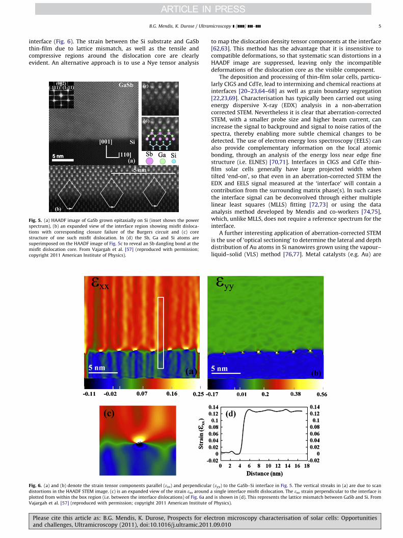
High angle annular dark field (HAADF) imaging [54] in theSTEM is particularly useful for characterising thin-film solar cellsbased on III–V and II-VI compound semiconductors (e.g. GaAs andCdTe) as well as chalcopyrite semiconductors (e.g. CIGS). Here anannular detector is used to collect the high angle scatteredelectrons, which are scattered from close to the atomic nucleus,so that the HAADF signal intensity varies as �Z1.7, where Z is theatomic number of the scattering atom. Hence pseudo-chemicalcontrast can also be observed in HAADF images. This is especiallyuseful for imaging crystal defects in thin-films as well as analys-ing polymorphs in III–V nanowires [55,56], which are potentialcandidates for nanowire-based solar cell devices (Section 2.2).HAADF has been used to image the atomic structure of interfacialmisfit dislocations in epitaxial III–V thin-films, as well as identifythe atomic species constituting any dangling bonds at thedislocation core [57,58]. Dangling bonds have an important effecton solar cell performance as they introduce deep energy levelswithin the band gap, consequently lowering the carrier lifetimethrough Shockley–Read–Hall recombination. As an exampleFig. 5a shows misfit dislocations at the interface between GaSband Si imaged using HAADF in an aberration-corrected STEM [57].Since all the atom columns are resolved a Burgers circuit analysiscan be carried out to determine the Burgers vector of theindividual dislocations (Fig. 5b). Furthermore, the chemical con-trast in the HAADF image enables the dangling bond at thedislocation core to be identified as an Sb atom (Figs. 5c and d).Despite the scan distortions present in STEM images due toelectrical interference [59] a geometric phase analysis [60,61]can qualitatively reveal the strain tensor components at the
ctron microscopy characterisation of solar cells: Opportunities.09.010
B.G. Mendis, K. Durose / Ultramicroscopy ] (]]]]) ]]]–]]] 5
interface (Fig. 6). The strain between the Si substrate and GaSbthin-film due to lattice mismatch, as well as the tensile andcompressive regions around the dislocation core are clearlyevident. An alternative approach is to use a Nye tensor analysis
Fig. 6. (a) and (b) denote the strain tensor components parallel (exx) and perpendicula
distortions in the HAADF STEM image. (c) is an expanded view of the strain exx around
plotted from within the box region (i.e. between the interface dislocations) of Fig. 6a an
Vajargah et al. [57] (reproduced with permission; copyright 2011 American Institute o
Fig. 5. (a) HAADF image of GaSb grown epitaxially on Si (inset shows the power
spectrum), (b) an expanded view of the interface region showing misfit disloca-
tions with corresponding closure failure of the Burgers circuit and (c) core
structure of one such misfit dislocation. In (d) the Sb, Ga and Si atoms are
superimposed on the HAADF image of Fig. 5c to reveal an Sb dangling bond at the
misfit dislocation core. From Vajargah et al. [57] (reproduced with permission;
copyright 2011 American Institute of Physics).
Please cite this article as: B.G. Mendis, K. Durose, Prospects for eleand challenges, Ultramicroscopy (2011), doi:10.1016/j.ultramic.2011
to map the dislocation density tensor components at the interface[62,63]. This method has the advantage that it is insensitive tocompatible deformations, so that systematic scan distortions in aHAADF image are suppressed, leaving only the incompatibledeformations of the dislocation core as the visible component.
The deposition and processing of thin-film solar cells, particu-larly CIGS and CdTe, lead to intermixing and chemical reactions atinterfaces [20–23,64–68] as well as grain boundary segregation[22,23,69]. Characterisation has typically been carried out usingenergy dispersive X-ray (EDX) analysis in a non-aberrationcorrected STEM. Nevertheless it is clear that aberration-correctedSTEM, with a smaller probe size and higher beam current, canincrease the signal to background and signal to noise ratios of thespectra, thereby enabling more subtle chemical changes to bedetected. The use of electron energy loss spectroscopy (EELS) canalso provide complementary information on the local atomicbonding, through an analysis of the energy loss near edge finestructure (i.e. ELNES) [70,71]. Interfaces in CIGS and CdTe thin-film solar cells generally have large projected width whentilted ‘end-on’, so that even in an aberration-corrected STEM theEDX and EELS signal measured at the ‘interface’ will contain acontribution from the surrounding matrix phase(s). In such casesthe interface signal can be deconvolved through either multiplelinear least squares (MLLS) fitting [72,73] or using the dataanalysis method developed by Mendis and co-workers [74,75],which, unlike MLLS, does not require a reference spectrum for theinterface.
A further interesting application of aberration-corrected STEMis the use of ‘optical sectioning’ to determine the lateral and depthdistribution of Au atoms in Si nanowires grown using the vapour–liquid–solid (VLS) method [76,77]. Metal catalysts (e.g. Au) are
r (eyy) to the GaSb–Si interface in Fig. 5. The vertical streaks in (a) are due to scan
a single interface misfit dislocation. The exx strain perpendicular to the interface is
d is shown in (d). This represents the lattice mismatch between GaSb and Si. From
f Physics).
ctron microscopy characterisation of solar cells: Opportunities.09.010
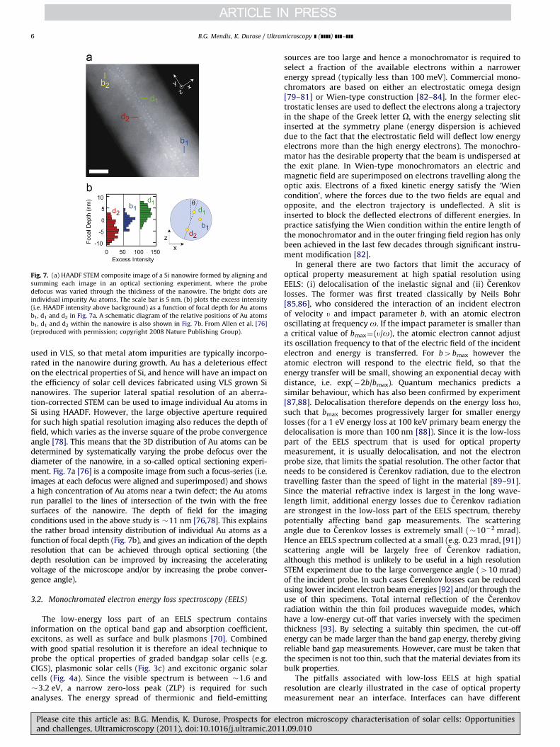
Fig. 7. (a) HAADF STEM composite image of a Si nanowire formed by aligning and
summing each image in an optical sectioning experiment, where the probe
defocus was varied through the thickness of the nanowire. The bright dots are
individual impurity Au atoms. The scale bar is 5 nm. (b) plots the excess intensity
(i.e. HAADF intensity above background) as a function of focal depth for Au atoms
b1, d1 and d2 in Fig. 7a. A schematic diagram of the relative positions of Au atoms
b1, d1 and d2 within the nanowire is also shown in Fig. 7b. From Allen et al. [76]
(reproduced with permission; copyright 2008 Nature Publishing Group).
B.G. Mendis, K. Durose / Ultramicroscopy ] (]]]]) ]]]–]]]6
used in VLS, so that metal atom impurities are typically incorpo-rated in the nanowire during growth. Au has a deleterious effecton the electrical properties of Si, and hence will have an impact onthe efficiency of solar cell devices fabricated using VLS grown Sinanowires. The superior lateral spatial resolution of an aberra-tion-corrected STEM can be used to image individual Au atoms inSi using HAADF. However, the large objective aperture requiredfor such high spatial resolution imaging also reduces the depth offield, which varies as the inverse square of the probe convergenceangle [78]. This means that the 3D distribution of Au atoms can bedetermined by systematically varying the probe defocus over thediameter of the nanowire, in a so-called optical sectioning experi-ment. Fig. 7a [76] is a composite image from such a focus-series (i.e.images at each defocus were aligned and superimposed) and showsa high concentration of Au atoms near a twin defect; the Au atomsrun parallel to the lines of intersection of the twin with the freesurfaces of the nanowire. The depth of field for the imagingconditions used in the above study is �11 nm [76,78]. This explainsthe rather broad intensity distribution of individual Au atoms as afunction of focal depth (Fig. 7b), and gives an indication of the depthresolution that can be achieved through optical sectioning (thedepth resolution can be improved by increasing the acceleratingvoltage of the microscope and/or by increasing the probe conver-gence angle).
3.2. Monochromated electron energy loss spectroscopy (EELS)
The low-energy loss part of an EELS spectrum containsinformation on the optical band gap and absorption coefficient,excitons, as well as surface and bulk plasmons [70]. Combinedwith good spatial resolution it is therefore an ideal technique toprobe the optical properties of graded bandgap solar cells (e.g.CIGS), plasmonic solar cells (Fig. 3c) and excitonic organic solarcells (Fig. 4a). Since the visible spectrum is between �1.6 and�3.2 eV, a narrow zero-loss peak (ZLP) is required for suchanalyses. The energy spread of thermionic and field-emitting
Please cite this article as: B.G. Mendis, K. Durose, Prospects for eleand challenges, Ultramicroscopy (2011), doi:10.1016/j.ultramic.2011
sources are too large and hence a monochromator is required toselect a fraction of the available electrons within a narrowerenergy spread (typically less than 100 meV). Commercial mono-chromators are based on either an electrostatic omega design[79–81] or Wien-type construction [82–84]. In the former elec-trostatic lenses are used to deflect the electrons along a trajectoryin the shape of the Greek letter O, with the energy selecting slitinserted at the symmetry plane (energy dispersion is achieveddue to the fact that the electrostatic field will deflect low energyelectrons more than the high energy electrons). The monochro-mator has the desirable property that the beam is undispersed atthe exit plane. In Wien-type monochromators an electric andmagnetic field are superimposed on electrons travelling along theoptic axis. Electrons of a fixed kinetic energy satisfy the ‘Wiencondition’, where the forces due to the two fields are equal andopposite, and the electron trajectory is undeflected. A slit isinserted to block the deflected electrons of different energies. Inpractice satisfying the Wien condition within the entire length ofthe monochromator and in the outer fringing field region has onlybeen achieved in the last few decades through significant instru-ment modification [82].
In general there are two factors that limit the accuracy ofoptical property measurement at high spatial resolution usingEELS: (i) delocalisation of the inelastic signal and (ii) Cerenkovlosses. The former was first treated classically by Neils Bohr[85,86], who considered the interaction of an incident electronof velocity u and impact parameter b, with an atomic electronoscillating at frequency o. If the impact parameter is smaller thana critical value of bmax¼(u/o), the atomic electron cannot adjustits oscillation frequency to that of the electric field of the incidentelectron and energy is transferred. For b4bmax however theatomic electron will respond to the electric field, so that theenergy transfer will be small, showing an exponential decay withdistance, i.e. exp(�2b/bmax). Quantum mechanics predicts asimilar behaviour, which has also been confirmed by experiment[87,88]. Delocalisation therefore depends on the energy loss :o,such that bmax becomes progressively larger for smaller energylosses (for a 1 eV energy loss at 100 keV primary beam energy thedelocalisation is more than 100 nm [88]). Since it is the low-losspart of the EELS spectrum that is used for optical propertymeasurement, it is usually delocalisation, and not the electronprobe size, that limits the spatial resolution. The other factor thatneeds to be considered is Cerenkov radiation, due to the electrontravelling faster than the speed of light in the material [89–91].Since the material refractive index is largest in the long wave-length limit, additional energy losses due to Cerenkov radiationare strongest in the low-loss part of the EELS spectrum, therebypotentially affecting band gap measurements. The scatteringangle due to Cerenkov losses is extremely small (�10�2 mrad).Hence an EELS spectrum collected at a small (e.g. 0.23 mrad, [91])scattering angle will be largely free of Cerenkov radiation,although this method is unlikely to be useful in a high resolutionSTEM experiment due to the large convergence angle (410 mrad)of the incident probe. In such cases Cerenkov losses can be reducedusing lower incident electron beam energies [92] and/or through theuse of thin specimens. Total internal reflection of the Cerenkovradiation within the thin foil produces waveguide modes, whichhave a low-energy cut-off that varies inversely with the specimenthickness [93]. By selecting a suitably thin specimen, the cut-offenergy can be made larger than the band gap energy, thereby givingreliable band gap measurements. However, care must be taken thatthe specimen is not too thin, such that the material deviates from itsbulk properties.
The pitfalls associated with low-loss EELS at high spatialresolution are clearly illustrated in the case of optical propertymeasurement near an interface. Interfaces can have different
ctron microscopy characterisation of solar cells: Opportunities.09.010
B.G. Mendis, K. Durose / Ultramicroscopy ] (]]]]) ]]]–]]] 7
optical properties due to chemical inter-diffusion, e.g. the CdSxTe1�x
interfacial layer in CdTe solar cells (Section 2.2). Consider the case ofan electron beam moving parallel to, but at a finite distance, from asharp interface between two materials A and B (the electron isincident in material B). As the impact parameter decreases, aninterface energy loss spectrum, of the form Im{�2/(eAþeB)}, isobserved and increases in intensity at the expense of the bulkenergy loss spectrum Im{�1/eB} for material B, i.e. the begrenzungs
effect (eA,B is the complex dielectric function and ‘Im’ represents theimaginary part) [94,95]. A Kramers–Kronig analysis [70] on such anEELS spectrum would give dielectric constants that are different tothe bulk material B, the difference being greater for smaller electronbeam impact parameters. Band gap measurements could alsobe affected. To see this note that the condition Im{eB}¼0 must besatisfied below the band gap of material B (this follows from therequirement that the bulk loss function is zero below the band gap,i.e. Im{�1/eB}¼0). However, if material A has a lower band gap,then Im{eAþeB}a0, and consequently Im{�2/(eAþeB)}a0, forenergies above the band gap of material A, i.e. a lower band gap ismeasured due to interface losses. The CdSxTe1�x inter-diffusionlayer at the CdS–CdTe interface in CdTe solar cells is more
pos 3
pos 2
pos 1 100 nm
1.62 eV
0.1 0.2 0.3 0.4 0.5 0.6 0.7 0.8 0.9 1.0
Fig. 8. (a) TEM bright field image of a Au nanorod suspended at the edge of a holey car
(d) show the distribution of different surface plasmon modes. The results were acq
permission; Copyright 2009 American Physical Society).
Please cite this article as: B.G. Mendis, K. Durose, Prospects for eleand challenges, Ultramicroscopy (2011), doi:10.1016/j.ultramic.2011
complicated than the sharp A–B interface discussed above. In thesimplest approximation, where the variation in sulphur concentra-tion within the inter-diffused layer is neglected, the material can berepresented as an A–B–C multi-layer, where ‘A’ is CdS, ‘B’ isCdSxTe1�x of fixed composition and ‘C’ is CdTe. A–B as well as B–Cinterface losses are now present which, if the B-layer is sufficientlythin, will couple with one another to produce further perturbations[93,96]. Fortunately numerical methods are available to simulate theEELS spectrum in such multi-layer structures, provided the dielectricconstants of the individual layers are known [97]. The dielectricconstants for the A and C layers can be directly extracted from EELSmeasurements made far from their respective interfaces. ‘Best-fit’dielectric constants for the unknown B-layer can then be chosen tomatch experimental measurements made across the A–B–C multi-layer, so that in principle a reliable estimate of the interfacial (i.e.B-layer) optical properties can be extracted.
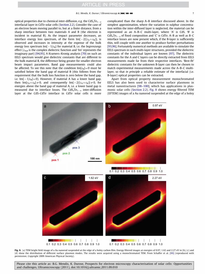
Apart from optical property measurement monochromatedEELS has also been used to characterise surface plasmons inmetal nanostructures [98–100], which has applications in plas-monic solar cells (Section 2.2). Fig. 8 shows energy filtered TEM(EFTEM) images of a Au nanorod suspended at the edge of a holey
2.27 eV
0.97 eV
0.1 0.2 0.3 0.4 0.5 0.6 0.7 0.8 0.9 1.0
0.1 0.2 0.3 0.4 0.5 0.6 0.7 0.8 0.9 1.0
bon film. Energy filtered images at energies of 0.97, 1.62 and 2.27 eV in (b), (c) and
uired using a monochromated TEM. From Schaffer et al. [99] (reproduced with
ctron microscopy characterisation of solar cells: Opportunities.09.010
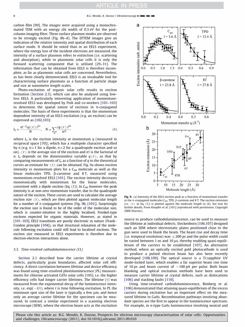
Fig. 9. (a) Intensity of the EELS exciton peak as a function of momentum transfer
in the p-conjugated molecules C60, TPD, b-carotene and 8 T. The exciton extension
(i.e. /rS in Eq. (1)) is plotted against the molecule length in (b). See text for
further details. From Knupfer et al. [101] (reproduced with permission; Copyright
2000 Elsevier).
B.G. Mendis, K. Durose / Ultramicroscopy ] (]]]]) ]]]–]]]8
carbon film [99]. The images were acquired using a monochro-mated TEM with an energy slit width of 0.3 eV for the post-column imaging filter. Three surface plasmon modes are observedto be strongly excited (Fig. 8b–d). The EFTEM images give anindication of the relative intensity and spatial distribution of eachsurface mode. It should be noted than in an EELS experiment,where the energy loss of the incident electrons are measured, theintensity of a surface plasmon refers to extinction (i.e. scatteringand absorption), while in plasmonic solar cells it is only theforward scattering component that is utilised [29–31]. Theinformation that can be obtained from EELS is therefore incom-plete, as far as plasmonic solar cells are concerned. Nevertheless,as has been clearly demonstrated, EELS is an invaluable tool forcharacterising surface plasmons as a function of particle shapeand size at nanometre length scales.
Photo-excitation of organic solar cells results in excitonformation (Section 2.3), which can also be analysed using low-loss EELS. A particularly interesting application of momentum-resolved EELS was developed by Fink and co-workers [101–103]to determine the spatial extent of excitons in p-conjugatedmolecules. The basis of these experiments is that the momentumdependent intensity of an EELS excitation (e.g. an exciton) can beexpressed as [102,103]:
Inpn!�2ðq/rSÞ2n
N, N¼
X
n
ðq/rSÞ2n
n!2ð1Þ
where In is the exciton intensity at momentum q (measured inreciprocal space [70]), which has a multipole character specifiedby n (e.g. n¼1 for a dipole, n¼2 for a quadrupole exciton and soon). /rS is the average size of the exciton and n! is the factorial ofn. In depends on the dimensionless variable q/rS, so that bycomparing measurements of In as a function of q to the theoreticalcurves an estimate for /rS can be obtained. Fig. 9a shows excitonintensity vs momentum plots for a C60 molecule as well as thelinear molecules TPD, b-carotene and 8 T, measured usingmomentum-resolved EELS [101]. The exciton intensity decreasesmonotonically with momentum for the linear molecules,consistent with a dipole exciton (Eq. (1)). In C60 however the peakintensity is at non-zero momentum transfer, due to the quadrupolenature of the exciton. These curves are used to calculate the averageexciton size /rS, which are then plotted against molecular lengthfor a number of p-conjugated systems (Fig. 9b, [101]). Surprisinglythe exciton size is found to be of the order of the molecular size,which is counter-intuitive to the highly localised, Frenkel-typeexcitons expected for organic materials. However, as stated in[101–103], EELS transitions are purely electronic in nature (Frank–Condon principle [104]), so that structural relaxation of the mole-cule following excitation could still lead to localised excitons. Theexciton size measured in EELS experiments is therefore due toelectron-electron interactions alone.
3.3. Time-resolved cathodoluminescence (CL)
Section 2.1 described how the carrier lifetime at crystaldefects, particularly grain boundaries, affected solar cell effi-ciency. A direct correlation between lifetime and device efficiencywas found using time-resolved photoluminescence (PL) measure-ments for chlorine activated CdTe solar cells [105], i.e. the higherefficiency cells had longer carrier lifetimes. The lifetime (t) wasmeasured from the exponential decay of the luminescence inten-sity, i.e. exp(�t/t), where t is time following excitation. In PL theminimum spot size of the laser is typically a few mm, and henceonly an average carrier lifetime for the specimen can be mea-sured. In contrast a similar experiment in a scanning electronmicroscope (SEM), where the electron beam acts as the excitation
Please cite this article as: B.G. Mendis, K. Durose, Prospects for eleand challenges, Ultramicroscopy (2011), doi:10.1016/j.ultramic.2011
source to produce cathodoluminescence, can be used to measurethe lifetime at individual defects. Steckenborn [106,107] designedsuch an SEM where electrostatic plates positioned close to thegun were used to blank the beam. The beam rise and decay time(i.e. temporal resolution) was r200 ps and the pulse width couldbe varied between 1 ns and 10 ms, thereby enabling quasi-equili-brium of the carriers to be established [107]. An alternativemethod, where an optically excited gold photocathode is usedto produce a pulsed electron beam has also been recentlydeveloped [108,109]. The optical source is a Ti:sapphire UVmode-locked laser, which enables a far superior beam rise timeof 10 ps and beam current of �100 pA per pulse. Both beamblanking and optical excitation methods have been used tomeasure carrier lifetime at crystal defects, such as dislocations[106] and stacking faults [110].
Using time-resolved cathodoluminescence, Bimberg et al.[106] demonstrated that attaining quasi-equilibrium of the excesscarriers during excitation has an important effect on the mea-sured lifetime in GaAs. Recombination pathways involving abun-dant species are the first to appear in the luminescence spectrum.For example, in n-type GaAs luminescence involving neutral and
ctron microscopy characterisation of solar cells: Opportunities.09.010
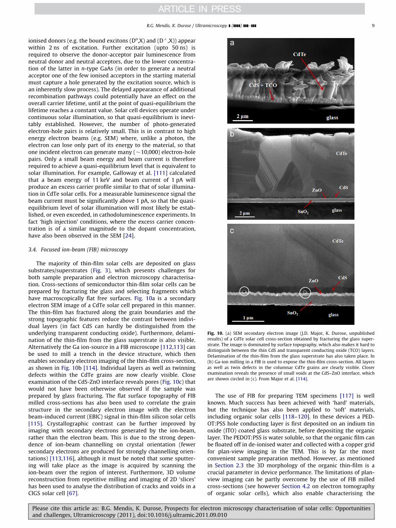
Fig. 10. (a) SEM secondary electron image (J.D. Major, K. Durose, unpublished
results) of a CdTe solar cell cross-section obtained by fracturing the glass super-
strate. The image is dominated by surface topography, which also makes it hard to
distinguish between the thin CdS and transparent conducting oxide (TCO) layers.
Delamination of the thin-film from the glass superstrate has also taken place. In
(b) Ga-ion milling in a FIB is used to expose the thin-film cross-section. All layers
as well as twin defects in the columnar CdTe grains are clearly visible. Closer
examination reveals the presence of small voids at the CdS–ZnO interface, which
are shown circled in (c). From Major et al. [114].
B.G. Mendis, K. Durose / Ultramicroscopy ] (]]]]) ]]]–]]] 9
ionised donors (e.g. the bound excitons (Do,X) and (Dþ ,X)) appearwithin 2 ns of excitation. Further excitation (upto 50 ns) isrequired to observe the donor-acceptor pair luminescence fromneutral donor and neutral acceptors, due to the lower concentra-tion of the latter in n-type GaAs (in order to generate a neutralacceptor one of the few ionised acceptors in the starting materialmust capture a hole generated by the excitation source, which isan inherently slow process). The delayed appearance of additionalrecombination pathways could potentially have an effect on theoverall carrier lifetime, until at the point of quasi-equilibrium thelifetime reaches a constant value. Solar cell devices operate undercontinuous solar illumination, so that quasi-equilibrium is inevi-tably established. However, the number of photo-generatedelectron-hole pairs is relatively small. This is in contrast to highenergy electron beams (e.g. SEM) where, unlike a photon, theelectron can lose only part of its energy to the material, so thatone incident electron can generate many (�10,000) electron-holepairs. Only a small beam energy and beam current is thereforerequired to achieve a quasi-equilibrium level that is equivalent tosolar illumination. For example, Galloway et al. [111] calculatedthat a beam energy of 11 keV and beam current of 1 pA willproduce an excess carrier profile similar to that of solar illumina-tion in CdTe solar cells. For a measurable luminescence signal thebeam current must be significantly above 1 pA, so that the quasi-equilibrium level of solar illumination will most likely be estab-lished, or even exceeded, in cathodoluminescence experiments. Infact ‘high injection’ conditions, where the excess carrier concen-tration is of a similar magnitude to the dopant concentration,have also been observed in the SEM [24].
3.4. Focused ion-beam (FIB) microscopy
The majority of thin-film solar cells are deposited on glasssubstrates/superstrates (Fig. 3), which presents challenges forboth sample preparation and electron microscopy characterisa-tion. Cross-sections of semiconductor thin-film solar cells can beprepared by fracturing the glass and selecting fragments whichhave macroscopically flat free surfaces. Fig. 10a is a secondaryelectron SEM image of a CdTe solar cell prepared in this manner.The thin-film has fractured along the grain boundaries and thestrong topographic features reduce the contrast between indivi-dual layers (in fact CdS can hardly be distinguished from theunderlying transparent conducting oxide). Furthermore, delami-nation of the thin-film from the glass superstrate is also visible.Alternatively the Ga ion-source in a FIB microscope [112,113] canbe used to mill a trench in the device structure, which thenenables secondary electron imaging of the thin-film cross-section,as shown in Fig. 10b [114]. Individual layers as well as twinningdefects within the CdTe grains are now clearly visible. Closeexamination of the CdS-ZnO interface reveals pores (Fig. 10c) thatwould not have been otherwise observed if the sample wasprepared by glass fracturing. The flat surface topography of FIBmilled cross-sections has also been used to correlate the grainstructure in the secondary electron image with the electronbeam-induced current (EBIC) signal in thin-film silicon solar cells[115]. Crystallographic contrast can be further improved byimaging with secondary electrons generated by the ion-beam,rather than the electron beam. This is due to the strong depen-dence of ion-beam channelling on crystal orientation (fewersecondary electrons are produced for strongly channelling orien-tations) [113,116], although it must be noted that some sputter-ing will take place as the image is acquired by scanning theion-beam over the region of interest. Furthermore, 3D volumereconstruction from repetitive milling and imaging of 2D ‘slices’has been used to analyse the distribution of cracks and voids in aCIGS solar cell [67].
Please cite this article as: B.G. Mendis, K. Durose, Prospects for eleand challenges, Ultramicroscopy (2011), doi:10.1016/j.ultramic.2011
The use of FIB for preparing TEM specimens [117] is wellknown. Much success has been achieved with ‘hard’ materials,but the technique has also been applied to ‘soft’ materials,including organic solar cells [118–120]. In these devices a PED-OT:PSS hole conducting layer is first deposited on an indium tinoxide (ITO) coated glass substrate, before depositing the organiclayer. The PEDOT:PSS is water soluble, so that the organic film canbe floated off in de-ionised water and collected with a copper gridfor plan-view imaging in the TEM. This is by far the mostconvenient sample preparation method. However, as mentionedin Section 2.3 the 3D morphology of the organic thin-film is acrucial parameter in device performance. The limitations of plan-view imaging can be partly overcome by the use of FIB milledcross-sections (see however Section 4.2 on electron tomographyof organic solar cells), which also enable characterising the
ctron microscopy characterisation of solar cells: Opportunities.09.010
B.G. Mendis, K. Durose / Ultramicroscopy ] (]]]]) ]]]–]]]10
roughness of individual layers and their interfaces [119,120].To the authors’ best knowledge a systematic study on ion-beamdamage and ion-beam heating during FIB sample preparation oforganic solar cells has not been carried out. Ion-beams comprisingof heavy Ga ions could potentially damage the covalent bondsalong polymer chains and/or the much weaker inter-chain vander Waal’s bonding. Furthermore, the temperature rise due toion-beam heating varies approximately inversely with thermalconductivity of the material [113]. Ion-beam heating is thereforeextremely important in organic solar cells, especially since theyare subjected to a short (30 min–1 h) anneal at only �150 1C,during which microstructural changes take place and the devicereaches peak efficiency [9]. The temperature rise during FIBmilling must therefore be kept well below the annealingtemperature.
4. Generic problems in solar cell characterisation
4.1. Grain boundary electrical activity in semiconductor thin-film
solar cells
The growth process for semiconductor thin-film solar cells,such as CdTe and CIGS, introduces a high density of grainboundaries that affects the device performance (Section 2.1)[17,22–24,65,121–125,150]. The recombination velocity of thegrain boundary has an important effect on carrier separation,
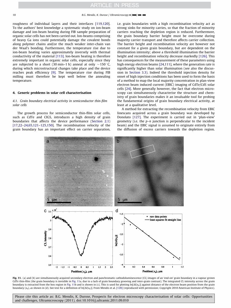
Fig. 11. (a) and (b) are simultaneously acquired secondary electron and panchromatic c
CdTe thin-film (the grain boundary is invisible in Fig. 11a, due to a lack of grain bound
boundary is extracted from the box region in Fig. 11b and is shown in (c). This is used f
boundary (xb), as shown in (d). See text for a definition of ln[DI(xb)]. From Mendis et al.
Please cite this article as: B.G. Mendis, K. Durose, Prospects for eleand challenges, Ultramicroscopy (2011), doi:10.1016/j.ultramic.2011
i.e. grain boundaries with a high recombination velocity act asstrong sinks for minority carries, so that the fraction of minoritycarriers reaching the depletion region is reduced. Furthermore,the grain boundary barrier height must be overcome duringmajority carrier transport and therefore affects carrier collection.The barrier height and recombination velocity are however notconstant for a given grain boundary, but are dependent on theillumination intensity; above a threshold illumination the barrierheight and recombination velocity decrease markedly [126]. Thishas consequences for the measurement of these parameters usinghigh energy electron beams [24,111], where the generation rate issignificantly higher than solar illumination (see also the discus-sion in Section 3.3). Indeed the threshold injection density foronset of high injection conditions has been used to form the basisof a method to map the local majority concentration in plan-viewelectron beam induced current (EBIC) imaging of CdTe/CdS solarcells [24]. More generally however, the fact that electron micro-scopy can simultaneously characterise the structure and chem-istry of grain boundaries makes it an invaluable tool for probingthe fundamental origins of grain boundary electrical activity, atleast at a qualitative level.
A method for extracting the recombination velocity from EBIClinescans acquired across a grain boundary was developed byDonolato [127]. The experiment is carried out in ‘plan-view’geometry (i.e. the p–n junction is perpendicular to the incidentbeam) and the EBIC signal is assumed to originate entirely fromthe diffusion of excess carriers towards the depletion region.
athodoluminescence (CL) images of an ‘end-on’ grain boundary in a vapour grown
ary grooving and inter-grain contrast). The integrated CL intensity across the grain
or plotting ln[DI(xb)] against distance of the electron beam position from the grain
[128] (reproduced with permission; Copyright 2010 American Institute of Physics).
ctron microscopy characterisation of solar cells: Opportunities.09.010
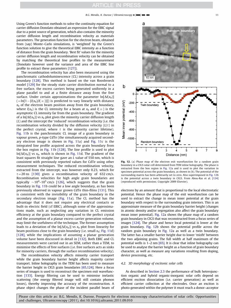
Fig. 12. (a) Phase map of the electron exit wavefunction for a random grain
boundary in a CIGS solar cell determined from TEM inline holography. The phase is
extracted from the box region in Fig. 12a and is used to plot the variation in
specimen potential across the grain boundary, as shown in (b). The potential of the
surrounding matrix has been arbitrarily set to zero. Also superimposed in Fig. 12b
is the potential across a twin boundary in CIGS. From Abou-Ras et al. [124]
(reproduced with permission; Copyright 2009 Elsevier).
B.G. Mendis, K. Durose / Ultramicroscopy ] (]]]]) ]]]–]]] 11
Using Green’s function methods to solve the continuity equation forcarrier diffusion Donolato obtained an expression for the EBIC signaldue to a point source of generation, which also contains the minoritycarrier diffusion length and recombination velocity as materialsparameters. The generation function for the electron beam, obtainedfrom (say) Monte–Carlo simulations, is ‘weighted’ by the Green’sfunction solution to give the theoretical EBIC intensity as a functionof distance from the grain boundary. ‘Best fit’ values for the minoritycarrier diffusion length and recombination velocity can be obtainedby matching the theoretical line profiles to the measurement(Donolato however used the variance and area of the EBIC lineprofile to extract these parameters [127]).
The recombination velocity has also been measured using thepanchromatic cathodoluminescence (CL) intensity across a grainboundary [128]. This method is based on the van Roosbroeckmodel [129] for the steady state carrier distribution normal to afree surface, the excess carriers being generated uniformly in aplane parallel to and at a finite distance away from the freesurface. Under certain approximations the parameter ln[DI(xb)](¼ ln[1�{I(xb)/I(N)}]) is predicted to vary linearly with distancexb of the electron beam position away from the grain boundary,where I(xb) is the CL intensity for a beam at xb and I(N) is theasymptotic CL intensity far from the grain boundary. The gradientof a ln[DI(xb)] vs xb plot gives the minority carrier diffusion length(L) and the intercept the ‘reduced’ recombination velocity (i.e. therecombination velocity divided by the diffusion velocity (L/t) inthe perfect crystal, where t is the minority carrier lifetime).Fig. 11b is the panchromatic CL image of a grain boundary invapour grown, p-type CdTe (the simultaneously acquired second-ary electron image is shown in Fig. 11a) and Fig. 11c is theintegrated line profile acquired across the grain boundary fromthe box region in Fig. 11b [128]. The line profile is used to plotln[DI(xb)] vs xb, which is shown in Fig. 11d. The gradient of theleast squares fit straight line gave an L value of 550 nm, which isconsistent with previously reported values for CdTe using othermeasurement techniques. The reduced recombination velocity,extracted from the intercept, was however only 0.23, which fort¼20 ns [130] gives a recombination velocity of 632 cm/s.Recombination velocities for high angle grain boundaries aretypically �104–105 cm/s [126], which suggests that the grainboundary in Fig. 11b could be a low angle boundary, as has beenpreviously observed in vapour grown CdTe thin-films [131]. Thisis consistent with the invisibility of the grain boundary in thesecondary electron image (Fig. 11a). The CL method has theadvantage that it does not require any electrical contacts orbuilt-in electric field (cf EBIC), although some of the approxima-tions made, such as neglecting any variation in CL emissionefficiency at the grain boundary compared to the perfect crystaland the assumption of a planar excess carrier generation volume,may limit the usefulness of the technique. The former assumptionleads to a deviation of the ln[DI(xb)] vs xb plot from linearity forbeam positions close to the grain boundary (i.e. small xb; Fig. 11d)[128], while the implications of assuming a planar generationvolume have been discussed in detail in [132]. Both EBIC and CLmeasurements were carried out in an SEM, rather than a TEM, tominimise the effects of free surfaces (i.e. free surfaces acts as sinksfor minority carriers, through the surface recombination velocity).
The recombination velocity affects minority carrier transportwhile the grain boundary barrier height affects majority carriertransport. Inline holography in the TEM has been used to measurethe barrier height in CIGS grain boundaries [65,124]. Here a focusseries of images is used to reconstruct the specimen exit wavefunc-tion [133]. Energy filtering can be used to minimise inelasticscattering (the energy filtered image will still contain phononlosses), thereby improving the accuracy of the reconstruction. Aphase object changes the phase of the incident parallel beam of
Please cite this article as: B.G. Mendis, K. Durose, Prospects for eleand challenges, Ultramicroscopy (2011), doi:10.1016/j.ultramic.2011
electrons by an amount that is proportional to the local electrostaticpotential. Hence the phase map of the exit wavefunction can beused to extract the change in mean inner potential at the grainboundary with respect to the surrounding grain interiors. This is anapproximate measure of the grain boundary barrier height (changesin atomic density and/or segregation also affect the grain boundarymean inner potential). Fig. 12a shows the phase map of a randomgrain boundary in CIGS that was reconstructed from a focus series ofimages [124]. The phase and hence local potential is lower at thegrain boundary. Fig. 12b shows the potential profile across therandom grain boundary in Fig. 12a as well as a twin boundary.The latter has a smaller barrier height due to lower ‘misfit’ betweenthe two adjoining grains. The full width at half maximum of thepotential wells is 1–2 nm [65]. It is clear that inline holography canbe used to analyse the barrier height as a function of grain boundarycharacter, as well as measure any variations resulting from doping,device processing, etc.
4.2. 3D morphology of excitonic solar cells
As described in Section 2.3 the performance of bulk heterojunc-tion organic and hybrid organic-inorganic solar cells depend onefficient exciton dissociation (i.e. carrier generation) as well asefficient carrier collection at the electrodes. Once an exciton isphoto-generated within the polymer it must reach a donor–acceptor
ctron microscopy characterisation of solar cells: Opportunities.09.010
B.G. Mendis, K. Durose / Ultramicroscopy ] (]]]]) ]]]–]]]12
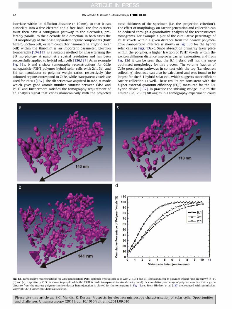
interface within its diffusion distance (�10 nm), so that it candissociate into a free electron and a free hole. The free carriersmust then have a contiguous pathway to the electrodes, pre-ferably parallel to the electrode field direction. In both cases the3D morphology of the phase separated organic components (bulkheterojunction cell) or semiconductor nanomaterial (hybrid solarcell) within the thin-film is an important parameter. Electrontomography [134,135] is a suitable method for characterising the3D morphology at nanometre spatial resolution and has beensuccessfully applied to hybrid solar cells [136,137]. As an exampleFig. 13a, b and c show tomography reconstructions for CdSenanoparticle–P3HT polymer hybrid solar cells with 2:1, 3:1 and6:1 semiconductor to polymer weight ratios, respectively (thecoloured regions correspond to CdSe, while transparent voxels areused for P3HT) [137]. The tilt series was acquired in HAADF modewhich gives good atomic number contrast between CdSe andP3HT and furthermore satisfies the tomography requirement ofan analysis signal that varies monotonically with the projected
Fig. 13. Tomography reconstructions for CdSe nanoparticle-P3HT polymer hybrid solar
(b) and (c), respectively. CdSe is shown in purple while the P3HT is made transparent fo
distance from the nearest polymer–semiconductor heterojunction is plotted for the to
Copyright 2011 American Chemical Society).
Please cite this article as: B.G. Mendis, K. Durose, Prospects for eleand challenges, Ultramicroscopy (2011), doi:10.1016/j.ultramic.2011
mass-thickness of the specimen (i.e. the ‘projection criterion’).The effect of morphology on carrier generation and collection canbe deduced through a quantitative analysis of the reconstructedtomograms. For example a plot of the cumulative percentage ofP3HT voxels within a given distance from the nearest polymer-CdSe nanoparticle interface is shown in Fig. 13d for the hybridsolar cells in Figs. 13a–c. Since absorption primarily takes placewithin the polymer, a higher fraction of P3HT voxels within theexciton diffusion distance improves carrier generation, and fromFig. 13d it can be seen that the 6:1 hybrid cell has the moreoptimised morphology for this process. The volume fraction ofCdSe percolation pathways in contact with the top (i.e. electroncollecting) electrode can also be calculated and was found to belargest for the 6:1 hybrid solar cell, which suggests more efficientcarrier collection as well. These results are consistent with thehigher external quantum efficiency (EQE) measured for the 6:1hybrid device [137]. In practice the ‘missing wedge’, due to thelimited (i.e. o901) tilt angles in a tomography experiment, could
cells with 2:1, 3:1 and 6:1 semiconductor to polymer weight ratio are shown in (a),
r visual clarity. In (d) the cumulative percentage of polymer voxels within a given
mograms in Fig. 13a–c. From Hindson et al. [137] (reproduced with permission;
ctron microscopy characterisation of solar cells: Opportunities.09.010
B.G. Mendis, K. Durose / Ultramicroscopy ] (]]]]) ]]]–]]] 13
have an effect on the accuracy of such quantitative analyses. Themissing wedge results in the reconstructed object to be elongatedalong the thin-film normal and can for example, lead to over-estimates for the connectivity of the nanoparticle network. This isparticularly relevant for carrier collection, since it is the connec-tivity of the nanoparticle network in the direction of the electrodefield, parallel to the thin-film normal, that is important, ratherthan the total connectivity. Furthermore, nanorods lying approxi-mately perpendicular to the tilt axis will only be weakly recon-structed due to the missing wedge. The missing wedge itself canbe minimised using a higher tilt angle [134] or through dual-axistomography experiments [138], which are however more timeconsuming.
Tomography of hybrid solar cells is relatively straightforward,since there is strong contrast between the inorganic and organiccomponents in the HAADF signal. This is however, not necessarily thecase for bulk heterojunction solar cells, especially P3HT-PCBM, wherecontrast is essentially due to small differences in mass-thicknessbetween carbon-rich phases. Conventional bright field imaging hashowever been used for tomography experiments on P3HT-PCBM[139,140] and other systems [141–143] (diffraction contrast in thebright field signal does not satisfy the projection criterion and willtherefore introduce artefacts in the reconstruction, although in thecase of P3HT–PCBM diffraction contrast is relatively weak and iseasily destroyed by electron beam damage of the specimen [135]).The quality of the reconstructed tomograms was suitable for extract-ing quantitative information, such as the distribution of P3HT‘nanowires’ through the thickness of the thin-film [139,140]. Analternative method for analysing carbonaceous materials was devel-oped by Gass et al. [144]. These authors used plasmon ratio maps asthe signal for tomographic reconstruction of a multi-wall carbonnanotube (MWCNT)-nylon composite. The (pþs) plasmon energy forMWCNT is 28 eV while for nylon it is 22 eV, so that a (22 eV/28 eV)energy filtered TEM ratio map gives strong contrast between the twocomponents (e.g. nylon-rich regions will appear bright in the ratiomap etc). Furthermore, the plasmon peak intensity increases mono-tonically with specimen thickness upto the plasmon mean free path,which for carbon-based materials is �180 nm for 300 kV electrons[144], so that with a suitably thin sample the projection criterion for atomography experiment can be satisfied. However, the techniquesuffers from the red-shift of the plasmon energy close to surfaces (i.e.surface plasmons) as well as delocalisation (Section 3.2). Neverthelessthe technique could be useful for bulk heterojunction solar cells,provided the plasmon energies for the donor and acceptor materialsare sufficiently different.
5. Conclusions
Many applications of electron microscopy characterisation in awide range of thin-film solar cell devices have been highlighted. Therecent advances in instrumentation have had a major impact in thedevelopment of this field. In particular it is now possible to extractquantitative information, such as the electrical properties of grainboundaries, nano-scale optical properties and 3D morphology ofexcitonic solar cells. Correlating these results with other measure-ments on device performance, such as quantum efficiency andcurrent-voltage characteristics, is important for understanding thefundamental physics governing device operation. This in turn couldlead to the future development of higher efficiency solar cells.
Acknowledgements
B.G. Mendis would like to thank EPSRC for financial support(grant EP/1028781/1) and K. Durose would like to thank the RCUK
Please cite this article as: B.G. Mendis, K. Durose, Prospects for eleand challenges, Ultramicroscopy (2011), doi:10.1016/j.ultramic.2011
Energy Programme—EPSRC SUPERGEN PV21—for financial sup-port (Grant EP/F029624/1).
References
[1] A. Goetzberger, C. Hebling, H.W. Schock, Materials Science & EngineeringR-Reports 40 (2003) 1.
[2] R.W. Birkmire, E. Eser, Annual Review of Materials Science 27 (1997) 625.[3] S. Guha, J. Yang, A. Banerjee, Progress in Photovoltaics: Research and
Applications. 8 (2000) 141.[4] M. Bosi, C. Pelosi, Progress in Photovoltaics: Research and Applications 15
(2007) 51.[5] K. Yu, J. Chen, Nanoscale Research Letters 4 (2009) 1.[6] Z. Fan, D.J. Ruebusch, A.A. Rathore, R. Kapadia, O. Ergen, P.W. Leu, A. Javey,
Nano Research 2 (2009) 829.[7] A.I. Hochbaum, P. Yang, Chemical Reviews 110 (2010) 527.[8] H. Spanggaard, F.C. Krebs, Solar Energy Materials and Solar Cells 83 (2004)
125.[9] B.C. Thompson, J.M.J. Frechet, Angewandte Chemie International Edition. 47
(2008) 58.[10] M. Gratzel, Progress in Photovoltaics: Research And Applications 8 (2000)
171.[11] S.K. Deb, in: Y. Hamakawa (Ed.), Thin-Film Solar Cells: Next Generation
Photovoltaics and its Applications, Springer-Verlag, Berlin Heidelberg, 2004,pp. 15–42.
[12] W. Shockley, H.J. Queisser, Journal of Applied Physics 32 (1961) 510.[13] J. Nelson, The Physics of Solar Cells, Imperial College Press, London, 2003.[14] Y. Hamakawa, in: Y. Hamakawa (Ed.), Thin-Film Solar Cells: Next Genera-
tion Photovoltaics and its Applications, Springer-Verlag, Berlin Heidelberg,2004, pp. 15–42.
[15] C. Wronski, D. Staebler, Applied Physics Letters 31 (1977) 292.[16] C. Wronski, D. Staebler, Journal of Applied Physics 51 (1980) 3262.[17] K. Durose, P.R. Edwards, D.P. Halliday, Journal of Crystal Growth 197 (1999)
733.[18] S. Mazzamuto, L. Vaillant, A. Bosio, N. Romeo, N. Armani, G. Salviati, Thin
Solid Films 516 (2008) 7079.[19] N. Romeo, A. Bosio, A. Romeo, Solar Energy Materials and Solar Cells 94
(2010) 2.[20] M. Emziane, K. Durose, N. Romeo, A. Bosio, D.P. Halliday, Thin Solid Films
480–481 (2005) 377.[21] M.D.G. Potter, D.P. Halliday, M. Cousins, K. Durose, Thin Solid Films
361–362 (2000) 248.[22] M. Terheggen, H. Heinrich, G. Kostorz, A. Romeo, D. Baetzner, A.N. Tiwari,
A. Bosio, N. Romeo, Thin Solid Films 431–432 (2003) 262.[23] M. Terheggen, H. Heinrich, G. Kostorz, D. Baetzner, A. Romeo, A.N. Tiwari,
Interface Science 12 (2004) 259.[24] P.R. Edwards, S.A. Galloway, K. Durose, Thin Solid Films 372 (2000) 284.[25] M.A. Contreras, K. Ramanathan, J.A. Shama, F. Hasoon, D.L. Young, B. Egass,
R. Noufi, Progress in Photovoltaics: Research and Applications 13 (2005)209.
[26] S. Schorr, Thin Solid Films 515 (2007) 5985.[27] D.B. Mitzi, O. Gunawan, T.K. Todorov, K. Wang, S. Guha, Solar Energy
Materials And Solar Cells 95 (2011) 1421.[28] I.D. Olekseyuk, I.V. Dudchak, L.V. Piskach, Journal of Alloys and Compounds
368 (2004) 135.[29] S. Pillai, M.A. Green, Solar Energy Materials and Solar Cells 94 (2010) 1481.[30] S. Pillai, K.R. Catchpole, T. Trupke, M.A. Green, Journal of Applied Physics
101 (2007) 093105.[31] T.L. Temple, G.D.K. Mahanama, H.S. Reehal, D.M. Bagnall, Solar Energy
Materials and Solar Cells 93 (2009) 1978.[32] E.C. Garnett, P.D. Yang, Journal of the American Chemical Society. 130
(2008) 9224.[33] B.Z. Tian, X.L. Zheng, T.J. Kempa, Y. Fang, N.F. Yu, G.H. Yu, J.L. Huang,
C.M. Lieber, Nature 449 (2007) 885.[34] B.L. Williams, B. Mendis, L. Bowen, D.P. Halliday, K. Durose, MRS proceed-
ings, in press.[35] T.M. Clarke, J.R. Durrant, Chemical Reviews. 110 (2010) 6736.[36] W.U. Huynh, J.J. Dittmer, A.P. Alivisatos, Science 295 (2002) 2425.[37] N.C. Greenham, X. Peng, A.P. Alivisatos, Physical Review B 54 (1996) 17628.[38] Y. Yu, P.V. Kamat, M. Kuno, Advanced Functional Materials 20 (2010) 1464.[39] B. O’Regan, M. Gratzel, Nature 353 (1991) 737.[40] K.D. Benkstein, N. Kopidakis, J. van de Lagemaat, A.J. Frank, Journal of
Physical Chemistry B 107 (2003) 7759.[41] O.L. Krivanek, P.D. Nellist, N. Dellby, M.F. Murfitt, Z. Szilagyi, Ultramicro-
scopy 96 (2003) 229.[42] P.E. Batson, N. Dellby, O.L. Krivanek, Nature 418 (2002) 617.[43] N. Dellby, O.L. Krivanek, P.D. Nellist, P.E. Batson, A.R. Lupini, Journal of
Electron Microscopy 50 (2001) 177.[44] O.L. Krivanek, G.J. Corbin, N. Dellby, B.F. Elston, R.J. Keyse, M.F. Murfitt,
C.S. Own, Z.S. Szilagyi, J.W. Woodruff, Ultramicroscopy 108 (2008) 179.[45] M. Haider, G. Braunshausen, E. Schwan, Optik 99 (1995) 167.[46] M. Haider, H. Rose, S. Uhlemann, B. Kabius, K. Urban, Journal of Electron
Microscopy 47 (1998) 395.
ctron microscopy characterisation of solar cells: Opportunities.09.010
B.G. Mendis, K. Durose / Ultramicroscopy ] (]]]]) ]]]–]]]14
[47] M. Haider, S. Uhlemann, E. Schwan, H. Rose, B. Kabius, K. Urban, Nature 392(1998) 769.
[48] J.L. Hutchison, J.M. Titchmarsh, D.J.H. Cockayne, R.C. Doole, C.J.D. Hetherington,A.I. Kirkland, H. Sawada, Ultramicroscopy 103 (2005) 7.
[49] M. Haider, P. Hartel, H. Muller, S. Uhlemann, J. Zach, Philosophical Transac-tions of the Royal Society of London Series A 367 (2009) 3665.
[50] U. Dahmen, R. Erni, V. Radmilovic, C. Kisielowski, M.D. Rossell, P. Denes,Philosophical Transactions of the Royal Society of London Series A 367(2009) 3795.
[51] M. Varela, S.D. Findlay, A.R. Lupini, H.M. Christen, A.Y. Borisevich, N. Dellby,O.L. Krivanek, P.D. Nellist, M.P. Oxley, L.J. Allen, S.J. Pennycook, PhysicalReview Letters 92 (2004) 095502.
[52] M. Bosman, V.J. Keast, J.L. Garcıa-Munoz, A.J. D’Alfonso, S.D. Findlay,L.J. Allen, Physical Review Letters 99 (2007) 086102.
[53] D.A. Muller, L. Fitting Kourkoutis, M. Murfitt, J.H. Song, H.Y. Hwang, J. Silcox,N. Dellby, O.L. Krivanek, Science 319 (2008) 1073.
[54] S.J. Pennycook, D.E. Jesson, Ultramicroscopy 37 (1991) 14.[55] G.E. Cirlin, V.G. Dubrovskii, B.Y. Samsonenko, A.D. Bouravleuv, K. Durose,
Y.Y. Proskuryakov, B. Mendis, L. Bowen, M.A. Kaliteevski, R.A. Abram,D. Zeze, Physical Review B 82 (2010) 035302.
[56] D. Spirkoska, J. Arbiol, A. Gustafsson, S. Conesa-Boj, F. Glas, I. Zardo,M. Heigoldt, M.H. Gass, A.L. Bleloch, S. Estrade, M. Kaniber, J. Rossler,F. Peiro, J.R. Morante, G. Abstreiter, L. Samuelson, A.F. Morral, PhysicalReview B 80 (2009) 245325.
[57] S.H. Vajargah, M. Couillard, K. Cui, S.G. Tavakoli, B. Robinson, R.N. Kleiman,J.S. Preston, G.A. Botton, Applied Physics Letters 98 (2011) 082113.
[58] S. Lopatin, S.J. Pennycook, J. Narayan, G. Duscher, Applied Physics Letters 81(2002) 2728.
[59] A.M. Sanchez, P.L. Galindo, S. Kret, M. Falke, R. Beanland, P.J. Goodhew,Journal of Microscopy 221 (2006) 1.
[60] M.J. Hytch, J.L. Putaux, J.M. Penisson, Nature 423 (2003) 270.[61] M.J. Hytch, E. Snoeck, R. Kilaas, Ultramicroscopy 74 (1998) 131.[62] B.G. Mendis, Y. Mishin, C.S. Hartley, K.J. Hemker, Philosophical Magazine 86
(2006) 4607.[63] C.S. Hartley, Y. Mishin, Acta Materialia 5 (2005) 1313.[64] Y. Yan, K.M. Jones, M.M. Al-Jassim, R. Dhere, X. Wu, Thin Solid Films (2010)
10.1016/j.tsf.2010.12.108.[65] D. Abou-Ras, J. Dietrich, J. Kavalakkatt, M. Nichterwitz, S.S. Schmidt,
C.T. Koch, R. Caballero, J. Klaer, T. Rissom, Solar Energy Materials and SolarCells 95 (2011) 1452.
[66] D. Abou-Ras, G. Kostorz, A. Romeo, D. Rudmann, A.N. Tiwari, Thin SolidFilms 480–481 (2005) 118.
[67] Z. Zhang, T. Wagner, Thin Solid Films 517 (2009) 4329.[68] V. Nadenau, D. Hariskos, H.W. Schock, M. Krejci, F.J. Haug, A.N. Tiwari,
H. Zogg, G. Kostorz, Journal of Applied Physics 85 (1999) 534.[69] K. Durose, M.A. Cousins, D.S. Boyle, J. Beier, D. Bonnet, Thin Solid Films
403–404 (2002) 396.[70] R.F. Egerton, Electron Energy Loss Spectroscopy in the Electron Microscope,
second edition, Plenum Press, New York, USA, 1996.[71] V.J. Keast, A.J. Scott, R. Brydson, D.B. Williams, J. Bruley, Journal of
Microscopy 203 (2001) 135.[72] M. MacKenzie, A.J. Craven, D.W. McComb, S. De Grendt, Applied Physics
Letters 88 (2006) 192112.[73] D.A. Muller, T. Sorsch, S. Moccio, F.H. Baumann, K. Evans-Lutterodt, G. Timp,
Nature 399 (1999) 758.[74] B.G. Mendis, M. MacKenzie, A.J. Craven, Ultramicroscopy 110 (2010) 105.[75] B.G. Mendis, A.J. Craven, Ultramicroscopy 111 (2011) 212.[76] J.E. Allen, E.R. Hemesath, D.E. Perea, J.L. Lensch-Falk, Z.Y. Li, F. Yin,
M.H. Gass, P. Wang, A.L. Bleloch, R.E. Palmer, L.J. Lauhon, Nature Nano-technology 3 (2008) 168.
[77] S.H. Oh, K. van Benthem, S.I. Molina, A.Y. Borisevich, W. Luo, P. Werner,N.D. Zakharov, D. Kumar, S.T. Pantelides, S.J. Pennycook, Nano Letters 8(2008) 1016.
[78] E.C. Cosgriff, P.D. Nellist, Ultramicroscopy 107 (2007) 626.[79] S. Uhlemann, M. Haider, in: Proceedings of ICEM-15, Durban, South Africa
(2002), vol. 3, page 327.[80] T. Walther, E. Quandt, H. Stegmann, A. Thesen, G. Benner, Ultramicroscopy
106 (2006) 963.[81] E. Essers, G. Benner, T. Mandler, S. Meyer, D. Mittmann, M. Schnell,
R. Hoschen, Ultramicroscopy 110 (2010) 971.[82] M. Terauchi, M. Tanaka, K. Tsuno, M. Ishida, Journal of Microscopy 194
(1999) 203.[83] P.E. Batson, Review of Scientific Instruments 43 (1986) 43.[84] K. Tsuno, Review of Scientific Instruments 64 (1993) 659.[85] N. Bohr, Philosophical Magazine. 25 (1913) 10.[86] R.F. Egerton, Ultramicroscopy 107 (2007) 575.[87] H. Kohl, H. Rose, Advances in Electronics and Electron Physics 65 (1985)
173.[88] D.A. Muller, J. Silcox, Ultramicroscopy 59 (1995) 195.[89] E. Kroger, Zeitschrift fur Physik 235 (1970) 403.[90] M. Stoger-Pollach, H. Franco, P. Schattschneider, S. Lazar, B. Schaffer,
W. Grogger, H.W. Zandbergen, Micron 37 (2006) 396.[91] M. Stoger-Pollach, Micron 39 (2008) 1092.[92] U. Kaiser, J. Biskupek, J.C. Meyer, J. Leschner, L. Lechner, H. Rose, M. Stoger-
Pollach, A.N. Khlobystov, P. Hartel, H. Muller, M. Haider, S. Eyhusen,G. Benner, Ultramicroscopy (2011). doi:10.1016/j.ultramic.2011.03.012.
Please cite this article as: B.G. Mendis, K. Durose, Prospects for eleand challenges, Ultramicroscopy (2011), doi:10.1016/j.ultramic.2011
[93] M. Couillard, A. Yurtsever, D.A. Muller, Physical Review B 77 (2008) 085318.[94] A. Howie, Ultramicroscopy 11 (1983) 141.[95] M.G. Walls, A. Howie, Ultramicroscopy 28 (1989) 40.[96] M. Couillard, M. Kociak, O. Stephan, G.A. Botton, C. Colliex, Physical Review
B 76 (2007) 165131.[97] J.P.R. Bolton, M. Chen, Ultramicroscopy 60 (1995) 247.[98] J. Nelayah, M. Kociak, O. Stephan, F.J. Garcia de Adajo, M. Tence, L. Henrard,
D. Taverna, I. Pastoriza-Santos, L.M. Liz-Marzan, C. Colliex, Nature Physics 3(2007) 348.
[99] B. Schaffer, U. Hohenester, A. Trugler, F. Hofer, Physical Review B 79 (2009)041401.
[100] B. Schaffer, K. Riegler, G. Kothleitner, W. Grogger, F. Hofer, Micron 40 (2009) 269.[101] M. Knupfer, J. Fink, E. Zojer, G. Leising, D. Fichou, Chemical Physics Letters.
318 (2000) 585.[102] M. Knupfer, T. Pichler, M.S. Golden, J. Fink, M. Murgia, R.H. Michel,
R. Zamboni, C. Taliani, Physical Review Letters 83 (1999) 1443.[103] M. Knupfer, J. Fink, Physical Review B 60 (1999) 10731.[104] M. Fox, Optical Properties of Solids, Oxford University Press, 2001.[105] D.P. Halliday, M.D.G. Potter, P. Dawson, in: Proceedings of the 28th IEEE
Photovoltaics Specialists Conference, Alaska 200, pp. 521–524.[106] A. Steckenborn, H. Munzel, D. Bimberg, Journal of Luminescence 24–25
(1981) 351.[107] D. Bimberg, H. Munzel, A. Steckenborn, J. Christen, Physical. Review. B 31
(1985) 7788.[108] M. Merano, S. Sonderegger, A. Crottini, S. Collin, P. Renucci, E. Pelucchi,
A. Malko, M.H. Baier, E. Kapon, B. Deveaud, J.D. Ganiere, Nature 438 (2005) 479.[109] M. Merano, S. Collin, P. Renucci, M. Gatri, S. Sonderegger, A. Crottini,
J.D. Ganiere, B. Deveaud, Review of Scientific Instruments 76 (2005) 085108.[110] P. Corfdir, P. Lefebvre, L. Balet, S. Sonderegger, A. Dussaigne, T. Zhu,
D. Martin, J.D. Ganiere, N. Grandjean, B. Deveaud-Pledran, Journal of AppliedPhysics 107 (2010) 043524.
[111] S.A. Galloway, P.R. Edwards, K. Durose, Solar Energy Materials and Solar.Cells 57 (1999) 61.
[112] L.A. Giannuzzi, F.A. Stevie, Introduction to Focused Ion Beams: Instrumenta-tion, Theory, Techniques and Practice, Springer, New York, USA, 2005.
[113] C.A. Volkert, A.M. Minor, MRS Bulletin 32 (2007) 389.[114] J.D. Major, L. Bowen, K. Durose, Progress in Photovoltaics: Research and
Applications (2011). doi:10.1002/pip.1164.[115] D. Inns, T. Puzzer, A.G. Aberle, Thin Solid Films 515 (2007) 3806.[116] B.W. Kempshall, S.M. Schwarz, B.I. Prenitzer, L.A. Giannuzzi, R.B. Irwin,
F.A. Stevie, Journal Of Vacuum Science And Technology B 19 (2001) 749.[117] L.A. Giannuzzi, F.A. Stevie, Micron 30 (1999) 197.[118] J. Loos, J.K.J. van Duren, F. Morrissey, R.A.J. Janssen, Polymer 43 (2002) 7493.[119] G.F. Malgas, C.J. Arendse, S. Mavundla, F.R. Cummings, Journal of Material
Sciences 43 (2008) 5599.[120] J.K.J. van Duren, J. Loos, F. Morrissey, C.M. Leewis, K.P.H. Kivits, L.J. van
Ijzendoorn, M.T. Rispens, J.C. Hummelen, R.A.J. Janssen, Advanced Func-tional Materials 12 (2002) 665.
[121] L.M. Woods, G.Y. Robinson, D.H. Levi, in: Proceedings of 28th IEEE Photo-voltaic Specialists Conference, 2000, p. 603.
[122] I. Visoly-Fisher, S.R. Cohen, A. Ruzin, D. Cahen, Advanced Materials 16(2004) 879.
[123] C.S. Jiang, R. Noufi, K. Ramanathan, J.A. AbuShama, H.R. Moutinho, M.M.Al-Jassim, Applied Physical Letters 85 (2004) 2625.
[124] D. Abou-Ras, C.T. Koch, V. Kustner, P.A. van Aken, U. Jahn, M.A. Contreras,R. Caballero, C.A. Kaufmann, R. Scheer, T. Unold, H.W. Schock, Thin SolidFilms 517 (2009) 2545.
[125] M.J. Romero, M.M. Al-Jassim, R.G. Dhere, F.S. Hasoon, M.A. Contreras,T.A. Gessert, H.R. Moutinho, Progress on Photovoltaics: Research andApplications 10 (2002) 445.
[126] J. Oualid, C.M. Singal, J. Dugas, J.P. Crest, H. Amzil, Journal of Applied Physics55 (1984) 1195.
[127] C. Donolato, Journal of Applied Physics 54 (1983) 1314.[128] B.G. Mendis, L. Bowen, Q.Z. Jiang, Applied Physical Letters 97 (2010) 092112.[129] W. van Roosbroeck, Journal of Applied Physics 26 (1955) 380.[130] D.R. Wight, D. Bradley, G. Williams, M. Astles, S.J.C. Irvine, C.A. Jones, Journal
of Crystal Growth 59 (1982) 323.[131] C.C.R. Watson, K. Durose, Journal of Crystal Growth 126 (1993) 325.[132] B.G. Mendis, L. Bowen, Journal of Physics: conference series (2011). doi:10.
1088/1742-6596/326/1/012017.[133] C.T. Koch, Ultramicroscopy 108 (2008) 141.[134] P.A. Midgley, M. Weyland, Ultramicroscopy 96 (2003) 413.[135] S.S. van Bavel, J. Loos, Advanced Functional Materials 20 (2010) 3217.[136] S.D. Oosterhout, M.M. Wienk, S.S. van Bavel, R. Thiedmann, L.J.A. Koster,
J. Gilot, J. Loos, V. Schmidt, R.A.J. Janssen, Nature Materials 8 (2009) 818.[137] J.C. Hindson, Z. Saghi, J.C. Hernandez-Garrido, P.A. Midgley, N.C. Greenham,
Nano Letters 11 (2011) 904.[138] I. Arslan, J.R. Tong, P.A. Midgley, Ultramicroscopy 106 (2006) 994.[139] S.S. van Bavel, E. Sourty, G. de With, J. Loos, Nano Letters 9 (2009) 507.[140] S.S. van Bavel, E. Sourty, G. de With, K. Frolic, J. Loos, Macromolecules 42
(2009) 7396.[141] X. Yang, J. Loos, Macromolecules 40 (2007) 1353.[142] S.S. van Bavel, E. Sourty, G. de With, S. Veenstra, J. Loos, Materials
Chemistry. 19 (2009) 5388.[143] B.V. Andersson, A. Herland, S. Masich, O. Inganass, Nano Letters 9 (2009) 853.[144] M.H. Gass, K.K.K. Koziol, A.H. Windle, P.A. Midgley, Nano Letters 6 (2006) 376.
ctron microscopy characterisation of solar cells: Opportunities.09.010

B.G. Mendis, K. Durose / Ultramicroscopy ] (]]]]) ]]]–]]] 15
[145] K. Durose, S.E. Asher, W. Jaegermann, D. Levi, B.E. McCandless, W. Metzger,H. Moutinho, P.D. Paulson, C.L. Perkins, J.R. Sites, G. Teeter, M. Terheggen,Progress in Photovoltaics: Research and Applications. 12 (2004) 177.
[146] J.D. Major, Y.Y. Proskuryakov, K. Durose, Progress in Photovoltaics: Researchand Applications (2011). doi:10.1002/pip.1196.
[147] H.R. Moutinho, F.S. Hasoon, F. Abulfotuh, L.L. Kazmerski, Journal of VacuumScience and Technology A 13 (1995) 2877.
Please cite this article as: B.G. Mendis, K. Durose, Prospects for eleand challenges, Ultramicroscopy (2011), doi:10.1016/j.ultramic.2011
[148] H.R. Moutinho, M.M. Al-Jassim, D.H. Levi, P.C. Dippo, L.L. Kazmerski, Journalof Vacuum Science and Technology A 16 (1998) 1251.
[149] M.A. Lourenco, Y.K. Yew, K.P. Homewood, K. Durose, H. Richter, D. Bonnet,Journal of Applied Physics. 82 (1997) 1423.
[150] L.M. Woods, D.H. Levi, G.Y. Robinson, V. Kaydanov, R. Ahrenkiel, in:Proceedings of the Seconnd World Conference on Photovoltaic EnergyConversion, Vienna, Austria, 1998, p. 1043.
ctron microscopy characterisation of solar cells: Opportunities.09.010