Project Report A 5.2 GHz Differential Cascode Low Noise ... · PDF fileA 5.2 GHz Differential...
43
Fourth Year Engineering Project Final Report Noah Moser i Project Report A 5.2 GHz Differential Cascode Low Noise Amplifier Noah Moser Supervisor: Dr. John Rogers April 2, 2004
Transcript of Project Report A 5.2 GHz Differential Cascode Low Noise ... · PDF fileA 5.2 GHz Differential...
Fourth Year Engineering Project Final Report
Noah Moser i
Project Report A 5.2 GHz Differential Cascode Low Noise Amplifier
Noah Moser Supervisor: Dr. John Rogers
April 2, 2004
Fourth Year Engineering Project Final Report
Noah Moser ii
ELEC 4907 – Fourth Year Engineering Project
Final Report
A 5.2 GHz Differential Cascode Low Noise Amplifier
Noah Moser
Project Supervisor: Dr. John Rogers
Carleton University, Department of Electronics
April 2, 2004
Fourth Year Engineering Project Final Report
Noah Moser iii
Abstract
As the demand for wireless network access increases so does the need for high
performance wireless Local Area Network (LAN) transceivers. One of the key
components of the wireless LAN transceiver is the Low-Noise Amplifier (LNA).
In this report, the design of a LNA to meet specifications is explained. The circuit was
built using the IBM sige5am bipolar process along with Cadence as a CAD tool.
Simulations using Cadence allowed the LNA to be optimized for better performance.
With the LNA designed, the physical layout of the amplifier was performed using
Cadence. The layout was performed to witness the effect of physical layout on the
LNA’s operation.
The design of the LNA was simulated in Cadence to verify its performance. In most
cases, the objectives of the project were met. However, recommendations for further
research and work are outlined in this report. The future work can be divided into work
on the circuit design, the integration of the LNA in a transceiver and development of
layout.
Fourth Year Engineering Project Final Report
Noah Moser iv
Table of Contents
List of Figures .................................................................................................................v List of Tables .................................................................................................................vi 1.0 Introduction...............................................................................................................1 2.0 Background Information............................................................................................2
2.1 Wireless LAN Transceivers ...................................................................................2 2.2 Specifications & Design Tools...................................................................................3
2.3 Group Members.....................................................................................................4 3.0 Low Noise Amplifier Theory.....................................................................................5
3.1 Introduction ...........................................................................................................5 3.2 Noise .....................................................................................................................5 3.3 Linearity ................................................................................................................6
4.0 Design Methodology .................................................................................................8 4.1 Amplifier Theory...................................................................................................8 4.2 Biasing ..................................................................................................................9 4.3 Tuned Tank .........................................................................................................12 4.4 Input Matching ....................................................................................................14 4.5 Output Buffer ......................................................................................................15 4.6 Single Ended Amplifier .......................................................................................18 4.7 Differential Amplifier ..........................................................................................20
5.0 Simulations..............................................................................................................22 5.1 Voltage Gain .......................................................................................................22 5.2 Input Impedance Matching ..................................................................................23 5.3 Linearity ..............................................................................................................25 5.4 Noise Figure ........................................................................................................26 5.5 Stability ...............................................................................................................26 5.6 DC Current ..........................................................................................................28 5.7 Summary of Simulation Results...........................................................................29
6.0 Layout .....................................................................................................................30 6.1 Layout Background .............................................................................................30 6.2 Layout Process ....................................................................................................31 6.3 Design Rule Check (DRC)...................................................................................33
7.0 Recommendations ...................................................................................................34 7.1 Circuit Improvement............................................................................................34 7.2 Integrating the LNA.............................................................................................34 7.3 Development of Layout .......................................................................................35 7.4 LNA Applications................................................................................................35
8.0 Conclusion ..............................................................................................................36 References.....................................................................................................................37
Fourth Year Engineering Project Final Report
Noah Moser v
List of Figures
Figure 1: Simplified block diagram of receiver end of radio ...........................................3 Figure 2: Common-emitter, common-base and common-collector amplifiers..................8 Figure 3: Simplified small signal model of the bipolar transistor.....................................9 Figure 4: Cascode amplifier............................................................................................9 Figure 5: Current mirror used to bias transistors ...........................................................10 Figure 6: Cascode transistor showing current mirror and resistor network.....................11 Figure 7: Cascode amplifier with inductors used for input matching .............................15 Figure 8: Simplified circuit showing output buffer and tuned tank ................................16 Figure 9: Single-ended LNA.........................................................................................18 Figure 10: S21 (Gain) of differential LNA .....................................................................23 Figure 11: S11 for input matched differential LNA.........................................................24 Figure 12: S11 parameter on Smith Chart ......................................................................24 Figure 13: Graph showing 1 dB Compression Point and Third-Order Intercept Point....25 Figure 14: Minimum noise figure and actual noise figure .............................................26 Figure 15: Kf from 100 MHz to 10 GHz.......................................................................27 Figure 16: Kf over a small frequency range ..................................................................27 Figure 17: B1f from 100 MHz to 10 GHz.....................................................................28 Figure 18: Layout schematic..........................................................................................33
Fourth Year Engineering Project Final Report
Noah Moser vi
List of Tables Table 1: LNA Specifications ..........................................................................................4 Table 2: Group members and components designed .......................................................4 Table 3: Transistor sizes ...............................................................................................19 Table 4: Sizing of inductors..........................................................................................19 Table 5: Capacitor sizes................................................................................................20 Table 6: Resistor sizes ..................................................................................................20 Table 7: Summary of simulation results........................................................................29
Fourth Year Engineering Project Final Report
Noah Moser 1
1.0 Introduction
The purpose of this project was the design of a Low Noise Amplifier (LNA) at 5.2 GHz
for wireless Local Area Network (LAN) applications. The LNA was designed to meet
specifications that were set to ensure that the LNA would be able to operate in a complete
receiver.
The field of Radio Frequency Integrated Circuit (RFIC) design is a growing one as a
result of increased demand for wireless products. LNAs are an essential part of wireless
LAN transceivers and as their demand increases so does the requirements for better
performance. Some pressing issues in the design of narrowband LNAs include the
linearity of the amplifier, noise added to the system by the amplifier and the quality of
integrated inductors.
The objectives of the project were:
a) to learn the RFIC design process
b) to design a LNA to meet specifications
c) to gain experience using CAD tools to build and simulate the LNA
d) work as part of an engineering team
This document provides background information and describes the tools used to build the
LNA. As well, it explains the design methodology of the LNA and provides and explains
simulation results. The layout process is discussed in this paper. Finally,
recommendations for others working on similar projects and for possible future work are
provided.
Fourth Year Engineering Project Final Report
Noah Moser 2
2.0 Background Information
In this section of the report, background information concerning the project will be
provided.
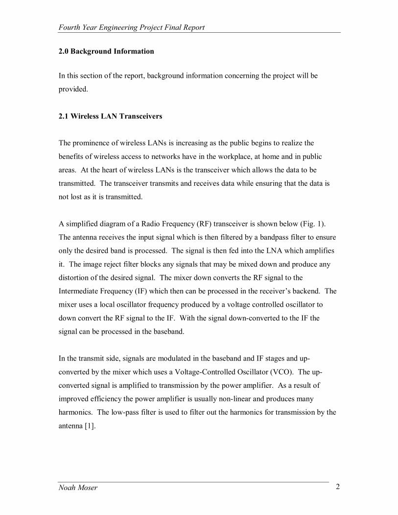
2.1 Wireless LAN Transceivers
The prominence of wireless LANs is increasing as the public begins to realize the
benefits of wireless access to networks have in the workplace, at home and in public
areas. At the heart of wireless LANs is the transceiver which allows the data to be
transmitted. The transceiver transmits and receives data while ensuring that the data is
not lost as it is transmitted.
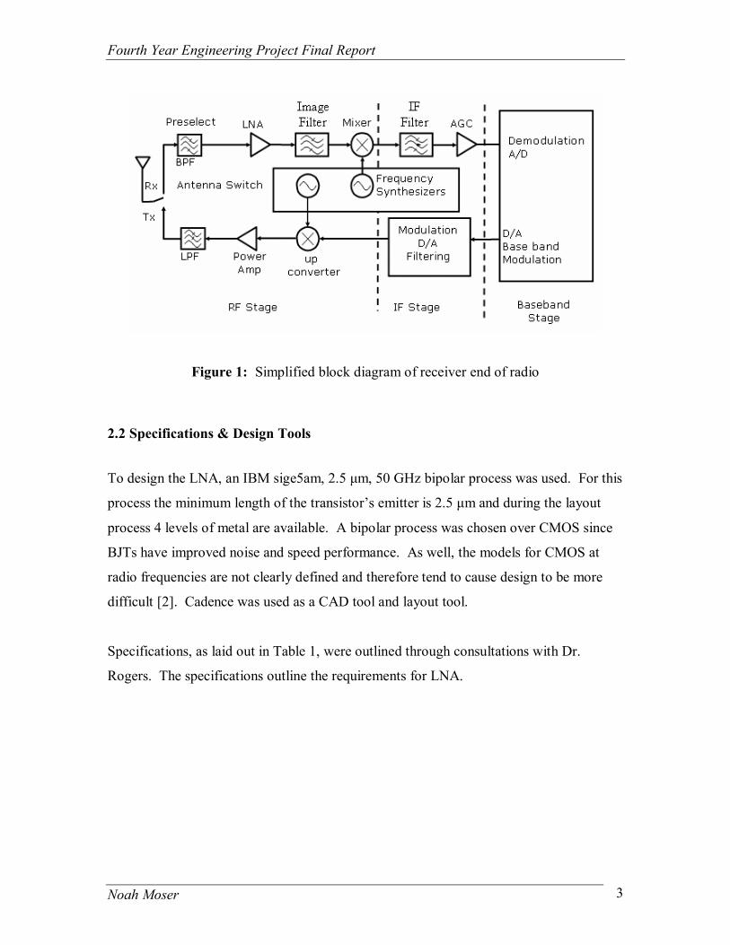
A simplified diagram of a Radio Frequency (RF) transceiver is shown below (Fig. 1).
The antenna receives the input signal which is then filtered by a bandpass filter to ensure
only the desired band is processed. The signal is then fed into the LNA which amplifies
it. The image reject filter blocks any signals that may be mixed down and produce any
distortion of the desired signal. The mixer down converts the RF signal to the
Intermediate Frequency (IF) which then can be processed in the receiver’s backend. The
mixer uses a local oscillator frequency produced by a voltage controlled oscillator to
down convert the RF signal to the IF. With the signal down-converted to the IF the
signal can be processed in the baseband.
In the transmit side, signals are modulated in the baseband and IF stages and up-
converted by the mixer which uses a Voltage-Controlled Oscillator (VCO). The up-
converted signal is amplified to transmission by the power amplifier. As a result of
improved efficiency the power amplifier is usually non-linear and produces many
harmonics. The low-pass filter is used to filter out the harmonics for transmission by the
antenna [1].
Fourth Year Engineering Project Final Report
Noah Moser 3
Figure 1: Simplified block diagram of receiver end of radio
2.2 Specifications & Design Tools
To design the LNA, an IBM sige5am, 2.5 µm, 50 GHz bipolar process was used. For this
process the minimum length of the transistor’s emitter is 2.5 µm and during the layout
process 4 levels of metal are available. A bipolar process was chosen over CMOS since
BJTs have improved noise and speed performance. As well, the models for CMOS at
radio frequencies are not clearly defined and therefore tend to cause design to be more
difficult [2]. Cadence was used as a CAD tool and layout tool.
Specifications, as laid out in Table 1, were outlined through consultations with Dr.
Rogers. The specifications outline the requirements for LNA.
Fourth Year Engineering Project Final Report
Noah Moser 4
Parameter Specification
Voltage Gain 15-20 dB
Centre frequency 5.2 GHz
Minimum bandwidth 200 MHz
Noise Figure ≤ 3 dB
Third-Order Intercept Point ≥ -20 dBm
Supply Voltage 3 V
DC Current ≤ 20 mA
Table 1: LNA Specifications
These specifications ensure that the LNA will provide sufficient gain with minimum
noise added while maintaining linearity.
2.3 Group Members
Each group member designed a component of the transceiver. In the table below, group
members and the components they designed are shown.
Andre Williams 5.2 GHz Colpitts Common Base Oscillator
Susan Yuen 2.4 GHz Differential Cascode LNA
Kenneth Ng 5.2 GHz Power Amplifier
Tarun Patel Broadband LNA
Hao Shan 5.2 GHz Power Amplifier
Table 2: Group members and components designed
Fourth Year Engineering Project Final Report
Noah Moser 5
3.0 Low Noise Amplifier Theory
This section will outline the purpose of the LNA. As well, important factors in the design
of the LNA will be explained.
3.1 Introduction
The input signals into the RF receiver are usually weak signals. Therefore, the LNA’s
principal purpose is to amplify weak signals. However, the LNA must not add significant
amounts of noise as noise limits how weak a signal can be for processing. Noise will be
a driving concern in the LNA so that other components in the receiver do not have to be
designed with noise as a major concern. Since the system will be receiving data, linearity
is a concern so that the integrity of the information is maintained. Linearity will cause
distortion which could result in the data being corrupted. As well, linearity limits how
large a signal can be [1].
3.2 Noise
Noise is present in any electrical system and is added by several sources. At higher
frequencies, the random movement of electrons is a main source of noise in a system. In
integrated circuits, noise is amplified by amplifiers and added by the random movement
of electrons in resistors, across junctions in transistors among other factors [2]. A
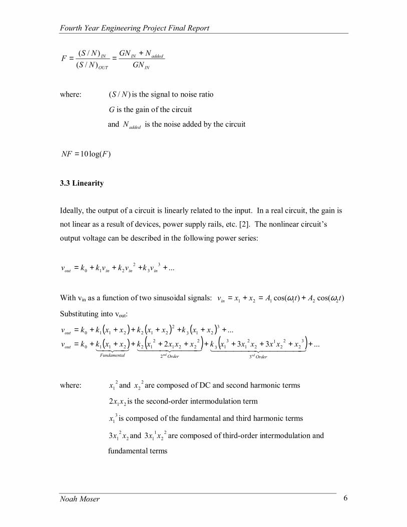
common measure of noise added to the system by the circuitry is the noise factor (F)
which, if measured in decibels, is known as the Noise Figure (NF).
Fourth Year Engineering Project Final Report
Noah Moser 6
IN
addedIN
OUT
IN
GNNGN
NSNS
F+
==)/()/(
where: )/( NS is the signal to noise ratio
G is the gain of the circuit
and addedN is the noise added by the circuit
)log(10 FNF =
3.3 Linearity
Ideally, the output of a circuit is linearly related to the input. In a real circuit, the gain is
not linear as a result of devices, power supply rails, etc. [2]. The nonlinear circuit’s
output voltage can be described in the following power series:
...33
2210 ++++= inininout vkvkvkkv
With vin as a function of two sinusoidal signals: )cos()cos( 221121 tAtAxxvin ωω +=+=
Substituting into vout:
( ) ( ) ( )( ) ( ) ( ) ...332
...
3
32
22
12
21
313
2
2221
2122110
3213
22122110
++++++++++=
+++++++=
44444 344444 21444 3444 2143421OrderOrderlFundamenta
out
out
rdnd
xxxxxxkxxxxkxxkkv
xxkxxkxxkkv
where: 21x and 2
2x are composed of DC and second harmonic terms
212 xx is the second-order intermodulation term
31x is composed of the fundamental and third harmonic terms
22
13 xx and 22
113 xx are composed of third-order intermodulation and
fundamental terms
Fourth Year Engineering Project Final Report
Noah Moser 7
The third-order intermodulation terms are undesired since they produce nonlinearity such
as intermodulation distortion and gain compression. As well, they are difficult to filter as
they are usually in the desired band. [2]
Fourth Year Engineering Project Final Report
Noah Moser 8
4.0 Design Methodology
In this section, the steps taken to design the LNA are explained. The topology of the
LNA is examined first, followed by a discussion on biasing the transistors. Input
matching is also discussed along with output buffers and differential amplifiers. Finally,
the sizing of the components is discussed.
4.1 Amplifier Theory
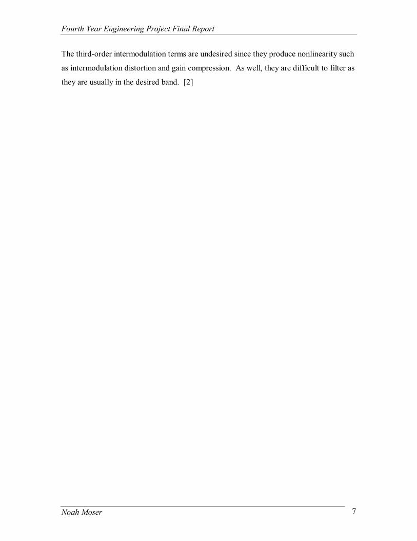
The three basic amplifier configurations for bipolar transistors are shown in Figure 2.
The common-emitter (CE) amplifier provides reasonable voltage gain and input and
output impedance however it suffers from limited bandwidth. The common-base (CB)
amplifier has a reasonable output impedance and voltage gain as well as high bandwidth
but it’s input impedance tends to be fairly low (approximately 25 Ω at 1 mA.) The
common-collector (CC) amplifier has high bandwidth and sufficient input impedance
however it has a voltage gain of approximately 1. [3]
Figure 2: Common-emitter, common-base and common-collector amplifiers
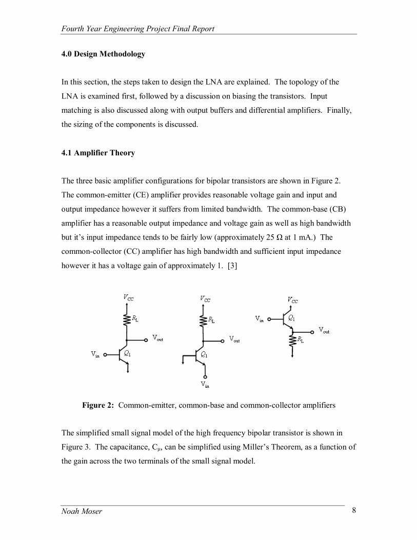
The simplified small signal model of the high frequency bipolar transistor is shown in
Figure 3. The capacitance, Cµ, can be simplified using Miller’s Theorem, as a function of
the gain across the two terminals of the small signal model.
Fourth Year Engineering Project Final Report
Noah Moser 9
Figure 3: Simplified small signal model of the bipolar transistor
The cascode amplifier, as seen in Figure 4, is built with a CE amplifier, Q1, acting as the
driver. With the addition of the CB amplifier, Q2, as the load of the CE, the frequency
response is improved as the low input impedance of the CB increases the dominant pole
frequency of the CE amplifier. However, the cascode amplifier must have a higher
supply voltage since voltage must be shared [4]. As well, there is a reduced signal swing
which can affect the linearity of the circuit.
Figure 4: Cascode amplifier
4.2 Biasing
To ensure that the transistors operate in the forward active region, proper biasing of the
transistors is required. The forward active region provides good gain and has improved
linearity and noise performance. For the BJTs to be in the forward active region, VC
Fourth Year Engineering Project Final Report
Noah Moser 10
must be greater than VB and VBE must be greater than the threshold voltage. In the case
of the transistors used at 5.2 GHz, VBE is approximately 0.9 V.
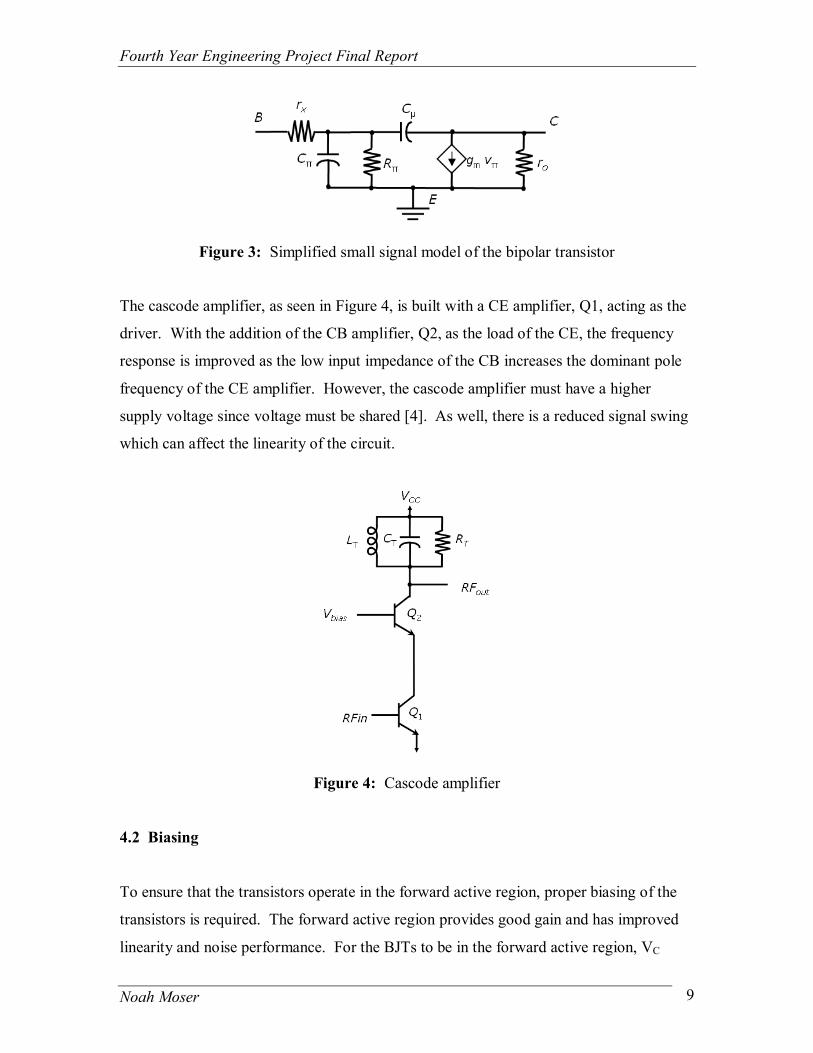
The use of a signal reference to bias the transistors ensures a dependable supply current
independent of temperature. The current mirror, as shown in Figure 5, has a current
reference as an input and produces a current N times greater than the current reference.
The chosen configuration for the current mirror has one of the mirror transistors also
acting as a driving transistor. As well, the input signal is inserted at the base of the
driving transistor. However, the base resistance is large enough compared to the input
impedance of the driving transistor which ensures that the input signal is fed into the
driving transistor. The additional transistor ensures that the base current is not affected
by loading of the transistor. The capacitor is able to reduce some of the noise created as a
result of the high transconductance of the driving transistor [2].
Figure 5: Current mirror used to bias transistors
Since ideal current sources are not available for integrated circuits, in the final circuit the
ideal current source was replaced with a resistor, Rref. The disadvantages of using a
resistor are that it will add to the noise of the system and will be temperature dependent.
The common-base transistor of the cascode amplifier can be biased by using a resistor
network as shown in Figure 6. The resistor network was designed to ensure that VB2 was
less than VC2 and 0.9 V above VE2. The resistor network was calculated as shown below.
as follows:
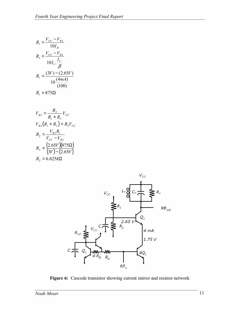
Fourth Year Engineering Project Final Report
Noah Moser 11
Ω=
−=
−=
−=
875)100()4(10
)65.2()3(
10
10
1
1
21
21
R
mAVVR
II
VVR
IVV
R
CC
BCC
B
BCC
β
( )
( )( )( ) ( )
Ω=−
Ω=
−=
=++
=
kRVV
VR
VVRVR
VRRRV
VRR
RV
BCC
B
CCB
CCB
625.665.23
87565.2
2
2
2
122
2212
21
22
Figure 6: Cascode transistor showing current mirror and resistor network
Fourth Year Engineering Project Final Report
Noah Moser 12
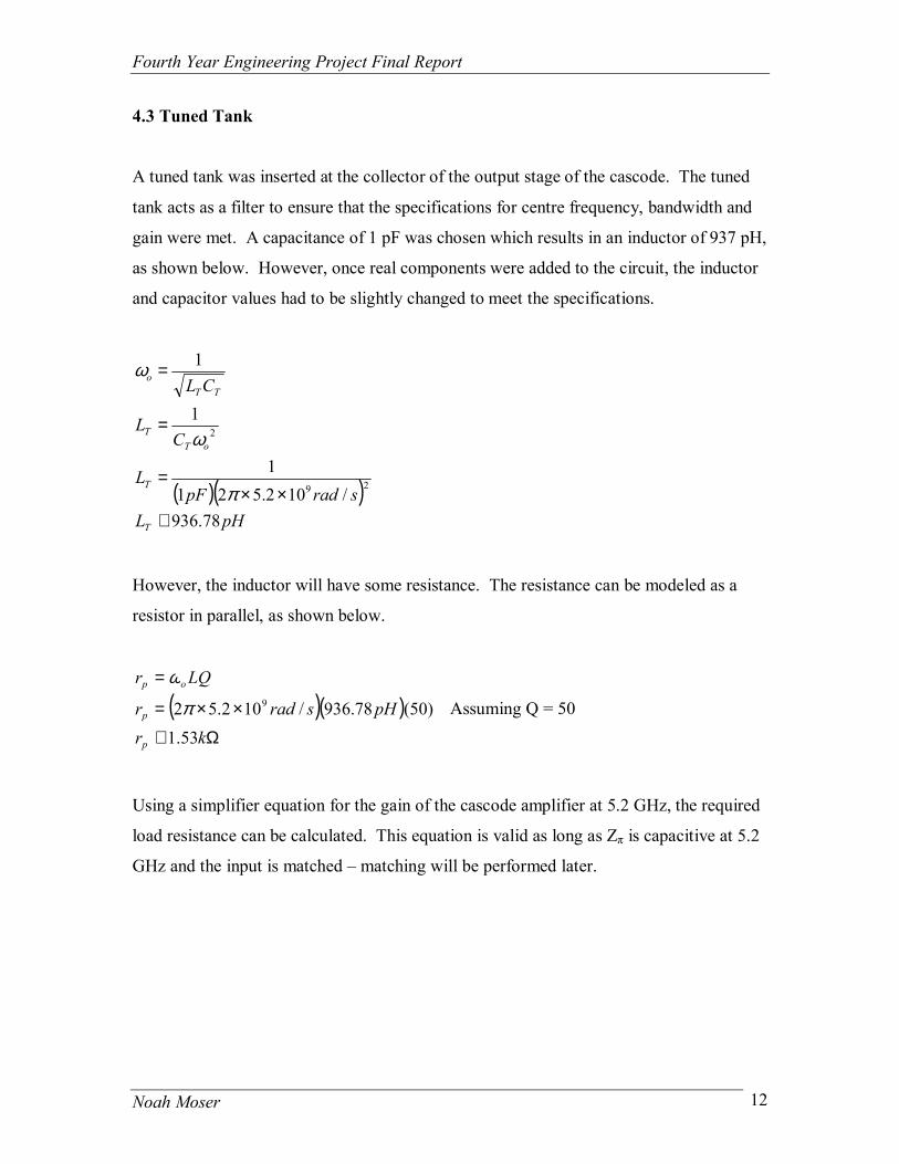
4.3 Tuned Tank
A tuned tank was inserted at the collector of the output stage of the cascode. The tuned
tank acts as a filter to ensure that the specifications for centre frequency, bandwidth and
gain were met. A capacitance of 1 pF was chosen which results in an inductor of 937 pH,
as shown below. However, once real components were added to the circuit, the inductor
and capacitor values had to be slightly changed to meet the specifications.
( )( )pHL
sradpFL
CL
CL
T
T
oTT
TTo
78.936/102.521
1
1
1
29
2
≅××
=
=
=
π
ω
ω
However, the inductor will have some resistance. The resistance can be modeled as a
resistor in parallel, as shown below.
( )( )Ω≅
××=
=
krpHsradr
LQr
p
p
op
53.1)50(78.936/102.52 9π
ω
Assuming Q = 50
Using a simplifier equation for the gain of the cascode amplifier at 5.2 GHz, the required
load resistance can be calculated. This equation is valid as long as Zπ is capacitive at 5.2
GHz and the input is matched – matching will be performed later.
Fourth Year Engineering Project Final Report
Noah Moser 13
( )( )( )( )( )
Ω≅
××Ω=
=
=
8.20716.0
407/102.525010
||
||
9
L
L
m
oSin
out
L
oS
Lm
in
out
R
fFsradR
g
CRvv
R
CRRg
vv
π
ω
ω
π
π
Set the gain to 20 dB = 10 V/V
With the load resistance calculated, the resistance required for the tuned tank can be
found as follows:
( ) ( )Ω≅
Ω−
Ω=
−=
=
24053.1
18.207
11
111||
T
T
pLT
pTL
RkR
rRR
rRR
The expected bandwidth can be calculated using the load resistance and the tuned tank
capacitor.
( )( )MHzBW
pFBW
CRBW
L
76618.207
1
1
≅Ω
=
=
Obviously, the bandwidth is wide. The bandwidth can be decreased by decreasing RL at
the expense of gain.
Fourth Year Engineering Project Final Report
Noah Moser 14
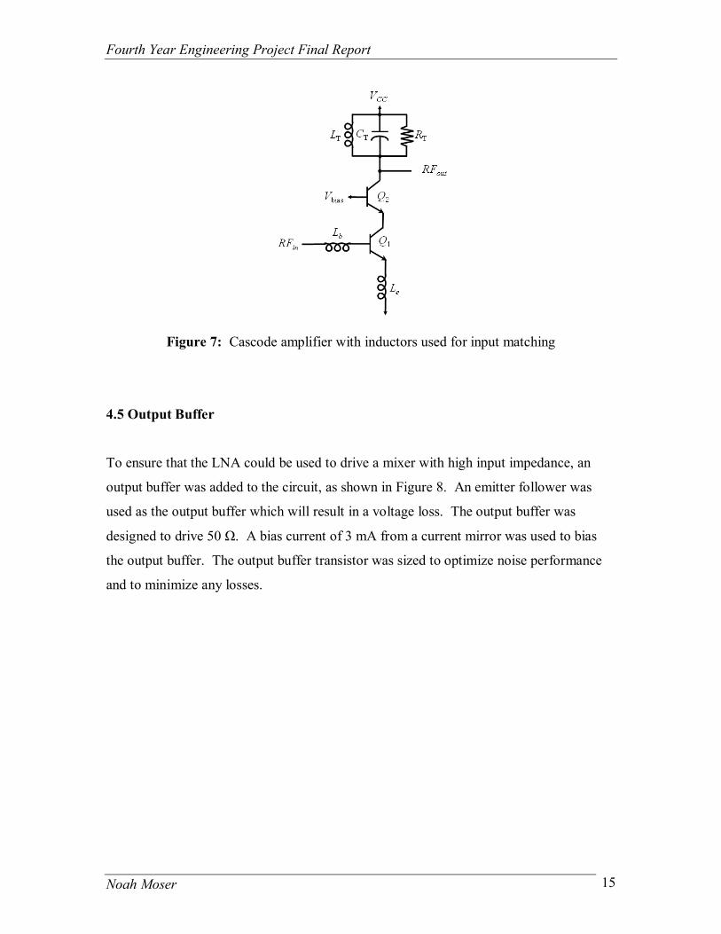
4.4 Input Matching
To improve the LNA’s performance in terms of gain, noise and power transfer, input
matching was performed. Two inductors, one connected to the base and another to the
emitter of the driver transistor as shown in Figure 7, can achieve simultaneous noise and
power matching. The first step of matching was to find the current density that would
ensure the lowest minimum noise figure. With the current density set, the emitter length
was chosen by sweeping the emitter lengths of the cascode transistors to find at which
point the real part of the optimum source impedance for the lowest noise figure was equal
to 50 Ω. The emitter length of the cascode transistors was set to 17.5 µm. The emitter
degeneration inductor was sized to match the real part of the input impedance to 50 Ω.
The base inductor was sized to lower the effect of the imaginary part of the input
impedance. The required emitter inductor was calculated, as shown below, to be
approximately 253.87 pH and the base inductor was calculated to be approximately
925.79 pH. However, through simulations these values were changed for proper
impedance matching.
( )( )
pHLVmAfFL
gCRL
e
e
m
Se
87.253)/4.156(
1.79450
≅
Ω=
= π
( )( )
pHL
pHsradfF
L
gCR
CL
b
b
m
Sb
79.925
)87.253(/102.521.794
1
1
29
2
≅
−××
=
−=
π
ωπ
π
Fourth Year Engineering Project Final Report
Noah Moser 15
Figure 7: Cascode amplifier with inductors used for input matching
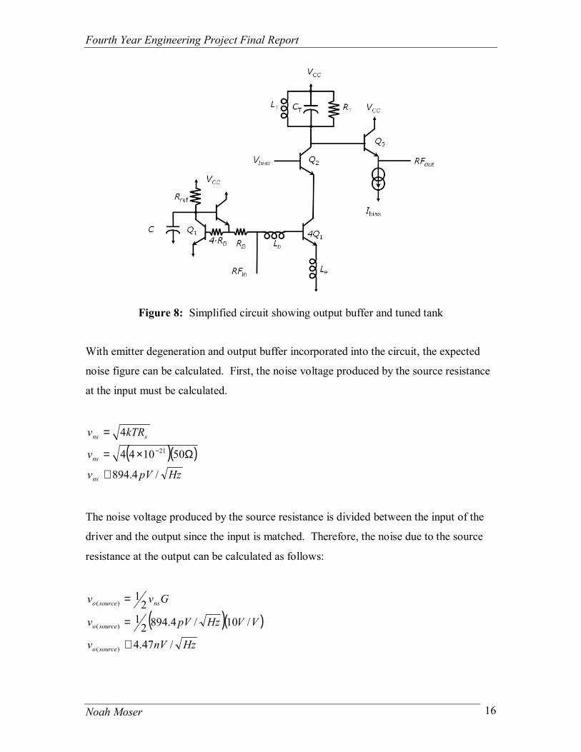
4.5 Output Buffer
To ensure that the LNA could be used to drive a mixer with high input impedance, an
output buffer was added to the circuit, as shown in Figure 8. An emitter follower was
used as the output buffer which will result in a voltage loss. The output buffer was
designed to drive 50 Ω. A bias current of 3 mA from a current mirror was used to bias
the output buffer. The output buffer transistor was sized to optimize noise performance
and to minimize any losses.
Fourth Year Engineering Project Final Report
Noah Moser 16
Figure 8: Simplified circuit showing output buffer and tuned tank
With emitter degeneration and output buffer incorporated into the circuit, the expected
noise figure can be calculated. First, the noise voltage produced by the source resistance
at the input must be calculated.
( )( )HzpVv
v
kTRv
ns
ns
sns
/4.894
501044
421
≅
Ω×=
=−
The noise voltage produced by the source resistance is divided between the input of the
driver and the output since the input is matched. Therefore, the noise due to the source
resistance at the output can be calculated as follows:
( )( )HznVv
VVHzpVv
Gvv
sourceo
sourceo
nssourceo
/47.4
/10/4.89421
21
)(
)(
)(
≅
=
=
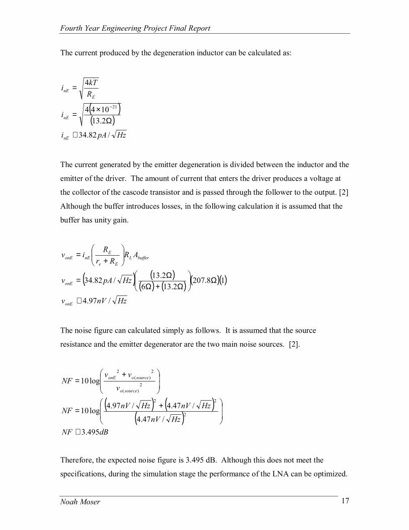
Fourth Year Engineering Project Final Report
Noah Moser 17
The current produced by the degeneration inductor can be calculated as:
( )( )
HzpAi
i
RkTi
nE
nE
EnE
/82.34
2.131044
4
21
≅
Ω×=
=
−
The current generated by the emitter degeneration is divided between the inductor and the
emitter of the driver. The amount of current that enters the driver produces a voltage at
the collector of the cascode transistor and is passed through the follower to the output. [2]
Although the buffer introduces losses, in the following calculation it is assumed that the
buffer has unity gain.
( ) ( )( ) ( ) ( )( )
HznVv
HzpAv
ARRr
Riv
onE
onE
bufferLEe
EnEonE
/97.4
18.2072.136
2.13/82.34
≅
Ω
Ω+Ω
Ω=
+
=
The noise figure can calculated simply as follows. It is assumed that the source
resistance and the emitter degenerator are the two main noise sources. [2].
( ) ( )( )
dBNFHznV
HznVHznVNF
v
vvNF
sourceo
sourceoonE
495.3/47.4
/47.4/97.4log10
log10
2
22
2)(
2)(
2
≅
+=
+=
Therefore, the expected noise figure is 3.495 dB. Although this does not meet the
specifications, during the simulation stage the performance of the LNA can be optimized.
Fourth Year Engineering Project Final Report
Noah Moser 18
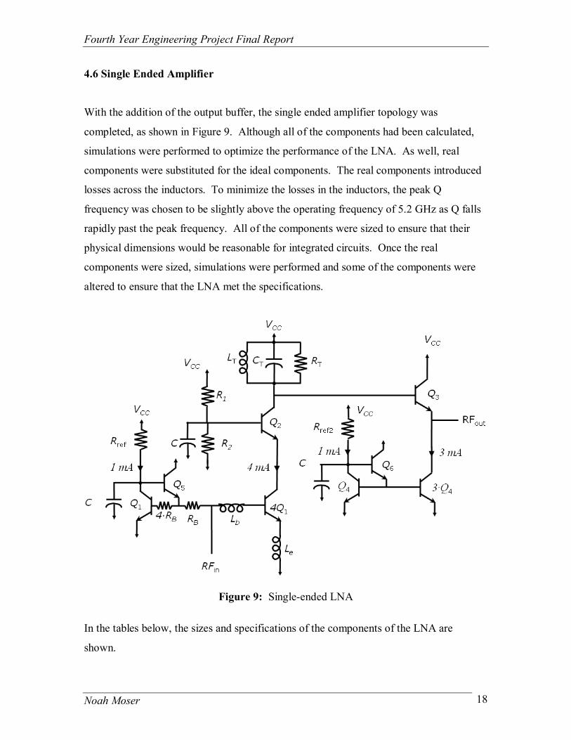
4.6 Single Ended Amplifier
With the addition of the output buffer, the single ended amplifier topology was
completed, as shown in Figure 9. Although all of the components had been calculated,
simulations were performed to optimize the performance of the LNA. As well, real
components were substituted for the ideal components. The real components introduced
losses across the inductors. To minimize the losses in the inductors, the peak Q
frequency was chosen to be slightly above the operating frequency of 5.2 GHz as Q falls
rapidly past the peak frequency. All of the components were sized to ensure that their
physical dimensions would be reasonable for integrated circuits. Once the real
components were sized, simulations were performed and some of the components were
altered to ensure that the LNA met the specifications.
Figure 9: Single-ended LNA
In the tables below, the sizes and specifications of the components of the LNA are
shown.
Fourth Year Engineering Project Final Report
Noah Moser 19
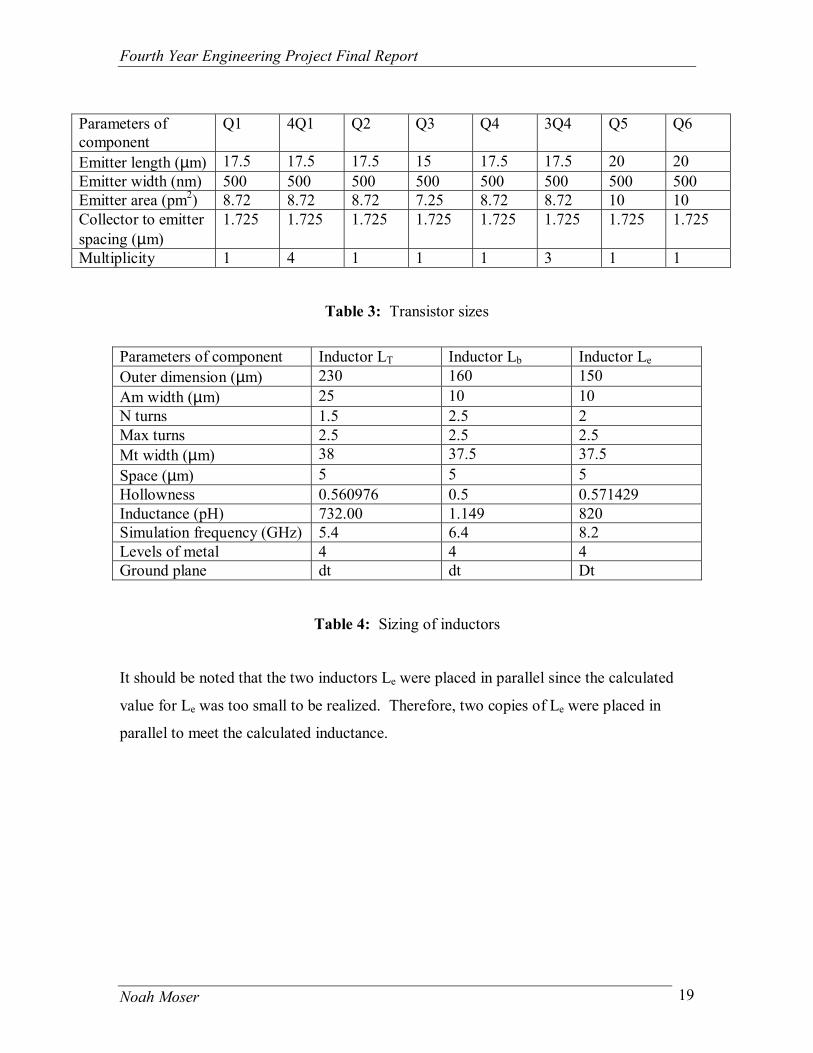
Parameters of component
Q1 4Q1 Q2 Q3 Q4 3Q4 Q5 Q6
Emitter length (µm) 17.5 17.5 17.5 15 17.5 17.5 20 20 Emitter width (nm) 500 500 500 500 500 500 500 500 Emitter area (pm2) 8.72 8.72 8.72 7.25 8.72 8.72 10 10 Collector to emitter spacing (µm)
1.725 1.725 1.725 1.725 1.725 1.725 1.725 1.725
Multiplicity 1 4 1 1 1 3 1 1
Table 3: Transistor sizes
Parameters of component Inductor LT Inductor Lb Inductor Le Outer dimension (µm) 230 160 150 Am width (µm) 25 10 10 N turns 1.5 2.5 2 Max turns 2.5 2.5 2.5 Mt width (µm) 38 37.5 37.5 Space (µm) 5 5 5 Hollowness 0.560976 0.5 0.571429 Inductance (pH) 732.00 1.149 820 Simulation frequency (GHz) 5.4 6.4 8.2 Levels of metal 4 4 4 Ground plane dt dt Dt
Table 4: Sizing of inductors
It should be noted that the two inductors Le were placed in parallel since the calculated
value for Le was too small to be realized. Therefore, two copies of Le were placed in
parallel to meet the calculated inductance.
Fourth Year Engineering Project Final Report
Noah Moser 20
Parameters of component Capacitor CT Capacitor C Cap coefficient (fF/µm2) 0.7 0.7 Backplate Dt Dt Capacitance effective (F) 1.06029 p 999.69 f Capacitance (F) 1.06029 p 999.69 f Length (µm) 40 50 µ Width (µm) 36.925 27.8 µ Multiplicity 1 1 Levels of metal 4 4
Table 5: Capacitor sizes
Parameters of component R1 R2 Rb 4Rb RT Rref Rref2
Width (µm) 10 5 10 2 10 10 10
Length (µm) 41.25 25.2 6.72 52.275 24.175 48.325 65.4
Resistance (Total) (Ω) 875.0 7.36 k 10.0 k 40.0 k 500.0 1.03 k 1.405 k
Resistance (Ω) 875.0 7.36 k 10.0 k 40.0 k 500.0 1.03 k 1.405 k
Simulation Temperature 25 25 25 25 25 25 25
Table 6: Resistor sizes
The resistors in the base of the driver transistors are quite large. They are required to be
large to ensure that the input signal, which is applied at the base of the driver is fed into
the transistor. A larger resistance than the input resistance of the driver ensures that the
signal follows the desired path.
4.7 Differential Amplifier
Once the single-ended circuit (Fig. 9) was designed, the amplifier was made differential -
this has several advantages. With the differential configuration, the amplifiers are now
referenced to each other instead of being referenced to the on-chip ground which is not
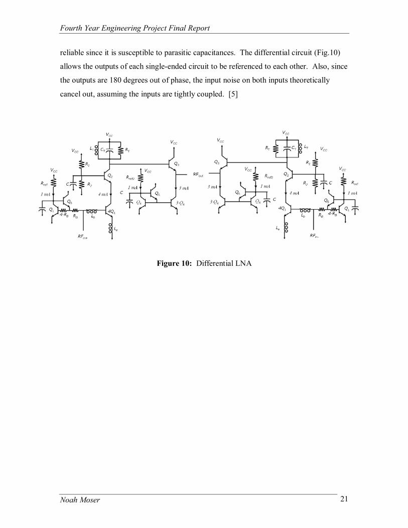
Fourth Year Engineering Project Final Report
Noah Moser 21
reliable since it is susceptible to parasitic capacitances. The differential circuit (Fig.10)
allows the outputs of each single-ended circuit to be referenced to each other. Also, since
the outputs are 180 degrees out of phase, the input noise on both inputs theoretically
cancel out, assuming the inputs are tightly coupled. [5]
Figure 10: Differential LNA
Fourth Year Engineering Project Final Report
Noah Moser 22
5.0 Simulations
With the differential circuit designed, simulations could be used to verify that the circuit
was meeting specifications as designed. Simulations were performed using DC, AC,
Noise, Scattering parameters (S-parameters) and Periodic Steady State (PSS) analyses.
These analyses allowed the circuits operation to be simulation including operating points
of the transistors, noise performance, gain, linearity, input impedance among others.
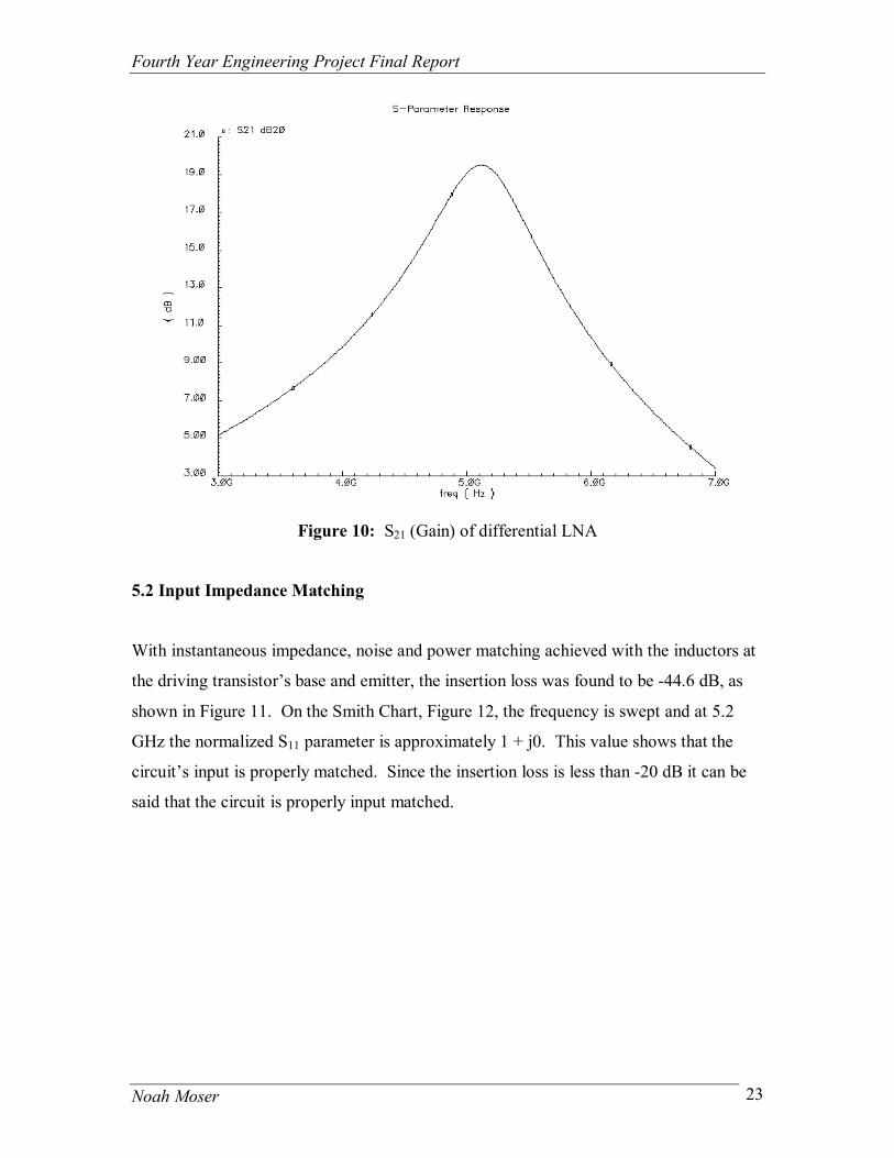
5.1 Voltage Gain
It can be seen from the graph below (Fig. 10) that the differential LNA has a voltage gain
of approximately 19.5 dB, a centre frequency of 5.2 GHz and a bandwidth of
approximately 700 MHz. This gain is sufficient to amplify any weak signal, but the gain
will drop when layout is performed. As well, the bandwidth is fairly large – this could be
decreased slightly to ensure that the amount of signal outside the wireless LAN being
amplified is minimized.
Fourth Year Engineering Project Final Report
Noah Moser 23
Figure 10: S21 (Gain) of differential LNA
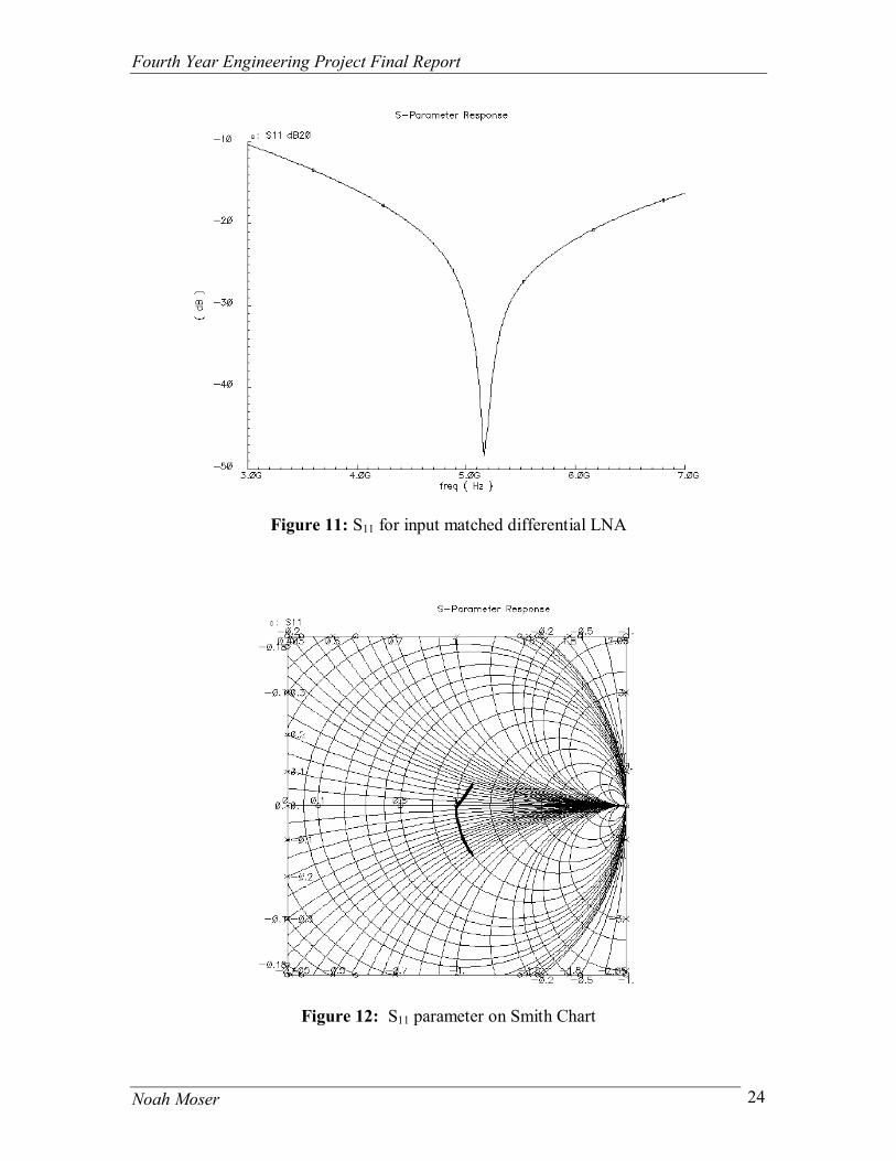
5.2 Input Impedance Matching
With instantaneous impedance, noise and power matching achieved with the inductors at
the driving transistor’s base and emitter, the insertion loss was found to be -44.6 dB, as
shown in Figure 11. On the Smith Chart, Figure 12, the frequency is swept and at 5.2
GHz the normalized S11 parameter is approximately 1 + j0. This value shows that the
circuit’s input is properly matched. Since the insertion loss is less than -20 dB it can be
said that the circuit is properly input matched.
Fourth Year Engineering Project Final Report
Noah Moser 24
Figure 11: S11 for input matched differential LNA
Figure 12: S11 parameter on Smith Chart
Fourth Year Engineering Project Final Report
Noah Moser 25
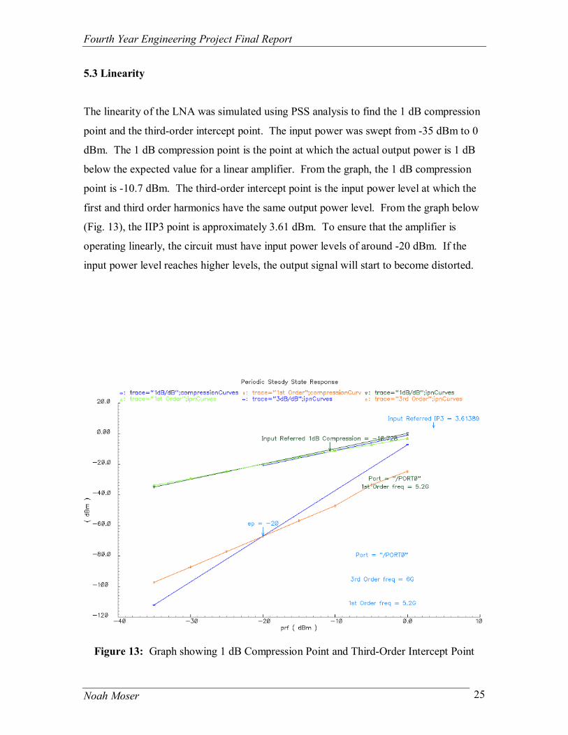
5.3 Linearity
The linearity of the LNA was simulated using PSS analysis to find the 1 dB compression
point and the third-order intercept point. The input power was swept from -35 dBm to 0
dBm. The 1 dB compression point is the point at which the actual output power is 1 dB
below the expected value for a linear amplifier. From the graph, the 1 dB compression
point is -10.7 dBm. The third-order intercept point is the input power level at which the
first and third order harmonics have the same output power level. From the graph below
(Fig. 13), the IIP3 point is approximately 3.61 dBm. To ensure that the amplifier is
operating linearly, the circuit must have input power levels of around -20 dBm. If the
input power level reaches higher levels, the output signal will start to become distorted.
Figure 13: Graph showing 1 dB Compression Point and Third-Order Intercept Point
Fourth Year Engineering Project Final Report
Noah Moser 26
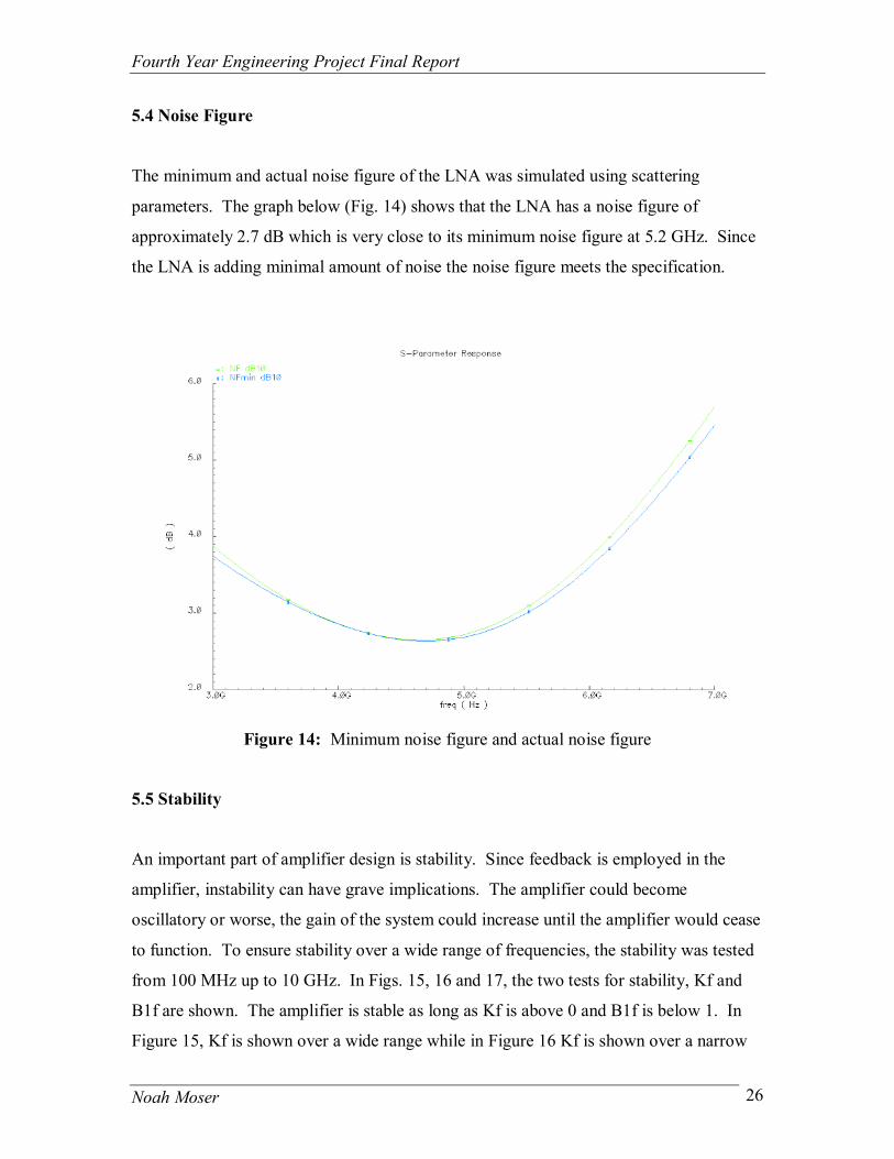
5.4 Noise Figure
The minimum and actual noise figure of the LNA was simulated using scattering
parameters. The graph below (Fig. 14) shows that the LNA has a noise figure of
approximately 2.7 dB which is very close to its minimum noise figure at 5.2 GHz. Since
the LNA is adding minimal amount of noise the noise figure meets the specification.
Figure 14: Minimum noise figure and actual noise figure
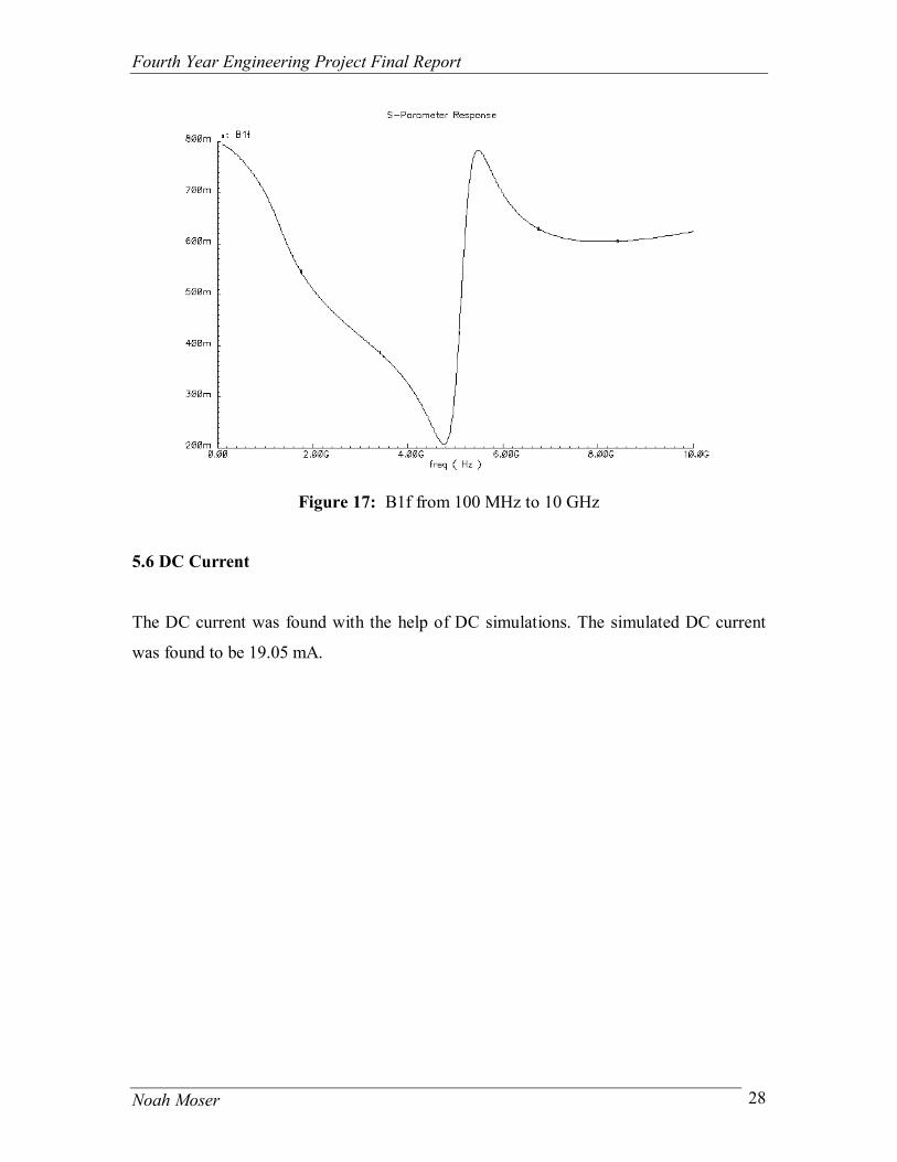
5.5 Stability
An important part of amplifier design is stability. Since feedback is employed in the
amplifier, instability can have grave implications. The amplifier could become
oscillatory or worse, the gain of the system could increase until the amplifier would cease
to function. To ensure stability over a wide range of frequencies, the stability was tested
from 100 MHz up to 10 GHz. In Figs. 15, 16 and 17, the two tests for stability, Kf and
B1f are shown. The amplifier is stable as long as Kf is above 0 and B1f is below 1. In
Figure 15, Kf is shown over a wide range while in Figure 16 Kf is shown over a narrow
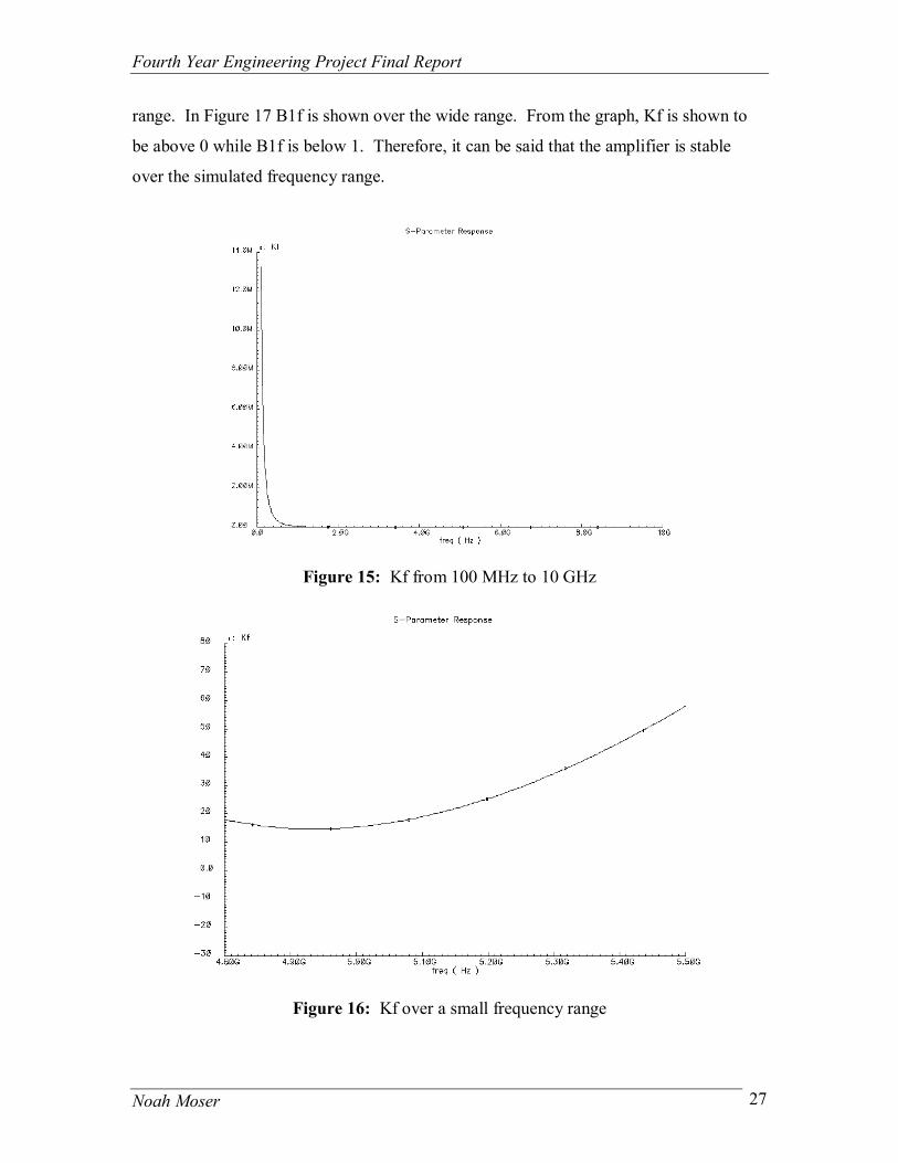
Fourth Year Engineering Project Final Report
Noah Moser 27
range. In Figure 17 B1f is shown over the wide range. From the graph, Kf is shown to
be above 0 while B1f is below 1. Therefore, it can be said that the amplifier is stable
over the simulated frequency range.
Figure 15: Kf from 100 MHz to 10 GHz
Figure 16: Kf over a small frequency range
Fourth Year Engineering Project Final Report
Noah Moser 28
Figure 17: B1f from 100 MHz to 10 GHz
5.6 DC Current
The DC current was found with the help of DC simulations. The simulated DC current
was found to be 19.05 mA.
Fourth Year Engineering Project Final Report
Noah Moser 29
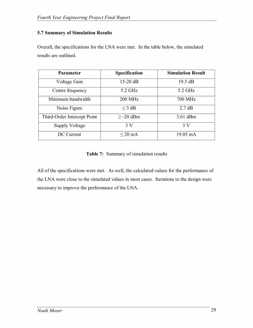
5.7 Summary of Simulation Results
Overall, the specifications for the LNA were met. In the table below, the simulated
results are outlined.
Parameter Specification Simulation Result
Voltage Gain 15-20 dB 19.5 dB
Centre frequency 5.2 GHz 5.2 GHz
Minimum bandwidth 200 MHz 700 MHz
Noise Figure ≤ 3 dB 2.7 dB
Third-Order Intercept Point ≥ -20 dBm 3.61 dBm
Supply Voltage 3 V 3 V
DC Current ≤ 20 mA 19.05 mA
Table 7: Summary of simulation results
All of the specifications were met. As well, the calculated values for the performance of
the LNA were close to the simulated values in most cases. Iterations to the design were
necessary to improve the performance of the LNA.
Fourth Year Engineering Project Final Report
Noah Moser 30
6.0 Layout
With the LNA designed, the final step was the layout process. The layout process allows
designers to have their circuits manufactured. Layout is an important step in RFIC
design for several reasons. Layout determines the physical area that the LNA will
occupy which is important as there are chip size specifications for wireless LAN
transceivers. As well, the area the LNA should be minimized since the chip area for
wireless LAN transceivers is limited. More importantly, the physical layout of the LNA
will have a direct impact on its performance. The performance is affected as the physical
layout introduces parasitics, coupling, matching as an issue and many other factors noted
included in the design of the LNA [2].
6.1 Layout Background
Layout was performed using the Cadence layout tool. The process that was used,
sige5am, allows for 4 levels of metal to be used; the first level of metal is the most
resistive while the top level of metal, the analog metal, is the least resistive. The metals
are separated by a polysilicon layer. A connection between the metal layers is achieved
using vias. Vias provide a path from one metal to another, however they introduce
resistance. To minimize the resistance, an array of vias can be implemented [2].
The inductors used in the design of the LNA were built using the analog metal, while the
Metal-Insulator-Metal (MIM) capacitors were built using two metal layers separated by
polysilicon. The layout of the transistors was performed by Cadence with connections to
the base, emitter and collector through the first and second levels of metal. The resistors
used in the LNA design were built in layout using polysilicon with connections at its
terminals through metal 1.
The signal paths made of the metals can be characterized as resistors. Like any metal, the
resistance is higher the thinner and longer the metal is while the resistance is lower when
the metal is wider and shorter. It is advantageous to have the RF signals or signals
Fourth Year Engineering Project Final Report
Noah Moser 31
traveling a long distance on the chip transmitted between components in the analog
metal. This would ensure that any losses would be minimized. Conversely, DC paths
can be implemented using the lower level, more resistive metals [2]. Electrons flow with
greater ease in straight paths; therefore, to minimize losses in the RF signal their paths
should be as straight as possible. As well, electron movement can cause the path’s atoms
to move, known as electromigration. Over time if enough metal is moved there can be a
loss of contact between metal paths [6]. Therefore, each metal level has a required width
per mA of DC current flowing in the path.
Parasitics, which are unwanted capacitances, resistances, etc., are created in the physical
layout as a result of many factors. Different levels of metal that overlap will create a
capacitance since they are separated by an insulator. As well, metals of the same level
that are close to each other and separated will have a capacitance in the vertical plane.
The paths themselves introduce resistance which becomes more severe as the paths are
longer and thinner.
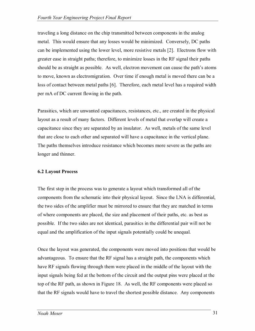
6.2 Layout Process
The first step in the process was to generate a layout which transformed all of the
components from the schematic into their physical layout. Since the LNA is differential,
the two sides of the amplifier must be mirrored to ensure that they are matched in terms
of where components are placed, the size and placement of their paths, etc. as best as
possible. If the two sides are not identical, parasitics in the differential pair will not be
equal and the amplification of the input signals potentially could be unequal.
Once the layout was generated, the components were moved into positions that would be
advantageous. To ensure that the RF signal has a straight path, the components which
have RF signals flowing through them were placed in the middle of the layout with the
input signals being fed at the bottom of the circuit and the output pins were placed at the
top of the RF path, as shown in Figure 18. As well, the RF components were placed so
that the RF signals would have to travel the shortest possible distance. Any components
Fourth Year Engineering Project Final Report
Noah Moser 32
that only passed DC signals were placed on the outside of the circuit and were positioned
to ensure that the paths were as short as possible. The components were placed to ensure
that inductors had approximately 5 times their line width of space surrounding them to
ensure that the quality factor, which affects the loss of the inductors, were maximized.
As well, transistors with multiplicity were placed together to ensure that the required
connections between them could be made as short as possible. Finally, multiple pins
were placed at strategic points surrounding the chip for the DC voltage source, ground
and substrate. Multiple pins ensure that the path lengths from the pins to the components
were minimized. Finally, each pin had a bond pad connected, allowing the circuit to have
connections off chip after fabrication. The completed layout is shown in Figure 18.
The next step in layout was connecting all of the nets from the schematic. With the help
of Cadence, all of the incomplete nets between components were identified. Metal paths
were used to connect the components. To minimize losses, RF signals were transmitted
in the analog metal and in straight paths, as much as possible. Arrays of vias between the
metal layers were used as much as possible since a single via has a higher resistance than
an array of vias.
Fourth Year Engineering Project Final Report
Noah Moser 33
Figure 18: Layout schematic
6.3 Design Rule Check (DRC)
Once the layout was generated and the incomplete nets were connected, the next step was
to verify that the layout met the design rules of the fabrication process. The design rules
specify the limitations of fabrication using the particular process. This verification was
performed using the DRC function of Cadence. The DRC test compares the layout to the
design rules of the process. When first performed, there were hundreds of DRC errors.
Through iterations, these errors were reduced. However, several errors concerning the
bond pads were created. At this point, the layout process was complete.
Fourth Year Engineering Project Final Report
Noah Moser 34
7.0 Recommendations
In this section, recommendations for future research and work are outlined. The
recommendations can be summarized as improvements to the circuit design, development
of layout, integrating the LNA with other components and other applications.
7.1 Circuit Improvement
There are several areas of the circuit design that can be improved. First, the resistors
used in the current mirror and DC bias resistor network to bias the transistors are
temperature dependent and add noise to the system. The use of bandgap reference
generators to generate the reference current is one possible area of research. Bandgap
reference generators are able to provide a bias that is temperate independent.
Although the circuit meets the specifications, improvements to the performance is still
possible. The noise created by the circuit can be minimized by increasing the gain of the
circuit. As well, the linearity can be improved by increasing the inductor in the emitter at
the expense of gain. From the simulations, it can be seen that the bandwidth is large.
Although a bandwidth which is too narrow is undesired, the simulated bandwidth can be
decreased by either increasing the capacitor or resistor in the tuned tank.
7.2 Integrating the LNA
One area of possible future work is the integration of the LNA with other components of
the transceiver. Although a complete transceiver was not designed by the group
members, some of the components can be attached and simulated. In particular, the LNA
at 5.2 GHz can be attached to the mixer, designed by a member of Dr. Plett’s project
group, which would also have one of the VCOs as a second input. On a larger scale, a
complete transceiver could be built and tested.
Fourth Year Engineering Project Final Report
Noah Moser 35
7.3 Development of Layout
One step to complete the layout would be to solve the DRC errors concerning the bond
pads. This would conclude the DRC step of the layout process.
With the DRC completed, the parasitics introduced by the physical layout must be
extracted. Extraction is an important step in layout as it allows the designer to properly
model the fabricated circuit. The extraction models all of the parasitics caused by layout
and allows the designer to see the affects of the physical layout on the circuit. Once the
parasitics are extracted, the Layout Versus Schematic (LVS) Check could be performed.
LVS verifies that the layout matches the original schematic. With a completed LVS
Check, the layout could be simulated. Post-layout simulations allow the designer to
verify that the circuit operates as expected after the layout process.
Finally, another area of possible research is the layout of inductors. The inductors
designed on-chip are the components that occupy the most amount of physical space on
the chip. Research in the area of integrated inductor design could yield many benefits. If
the size of the inductors was reduced, the total area of the chip could be reduced as well.
As the size of the chip decreases so does the cost of manufacturing the chip [5].
7.4 LNA Applications
Although the LNA was designed for a wireless LAN transceiver application, the LNA
could be modified to meet other needs. The area of RFIC design is expanding and many
new applications are being discovered continually. The LNA could be changed either to
meet different specifications on power consumption, gain, and chip area, among others.
Fourth Year Engineering Project Final Report
Noah Moser 36
8.0 Conclusion
Low Noise Amplifiers are an important component in RF transceivers as they amplify
weak signals so that the other components in the transceiver can process the signals. As
well, the LNA adds minimal noise to the system while maintaining linearity.
The 5.2 GHz differential cascode LNA was designed to operate in a wireless LAN
receiver. Using an IBM sige5am bipolar process, the LNA was designed to meet
specifications outlined by the project supervisor. The key issues in the design, gain,
noise and linearity were considered. The LNA was designed to provide gain and to
minimize the affect of noise on the AC operation of the circuit. Linearity was maintained
with the use of emitter degeneration along with ensuring that the bias voltages allowed
for a healthy signal swing.
The design began with selecting an appropriate topology. Since the models for bipolar
transistors are well defined, calculations were performed to size the components. With
calculated values, simulations allowed the performance of the LNA to be optimized.
Finally, layout was performed to examine the physical size of the LNA and its
components. During the layout process, the physical sizes of the components were
altered to minimize the chip area.
Overall, the objectives of the project were met. The design process of RFIC circuits was
examined in a group setting. As well, experience was gained in the use of CAD tools to
design and simulate RF circuits. Finally, the LNA was designed to meet specifications.
Fourth Year Engineering Project Final Report
Noah Moser 37
References
[1] Plett, Calvin, 97.455 Telecommunication Circuits: 2003 Course Notes, Labs plus:
Handouts, Exams, etc., 2003.
[2] Rogers, John, and Plett, Calvin, Radio Frequency Integrated Circuit Design,
Norwood, MA: Artech House, 2003.
[3] Chan, Plett, Ray, and Zhang, 97.359 Electronics II Lecture Notes 2002/2003, 2002.
[4] Sedra and Smith, Microelectronics Circuits, New York, NY: Oxford University
Press, 1998.
[5] MacEachern, Leonard, ELEC 4707 Analog Integrated Electronics Course Notes,
2004.
[6] Walkey, David J., 97.398 Physical Electronics Course Notes, 2002.


![Cascode Switching Modeling and Improvement in Flyback ...Cascode GaN FET [10], during inductive hard switching. Figure 2 Cascode Switching Configured Flyback converter II. MODELING](https://static.fdocuments.net/doc/165x107/5e541119f61a9f6e2b2e813c/cascode-switching-modeling-and-improvement-in-flyback-cascode-gan-fet-10.jpg)