CATA Curricular Code Agronomy Contest (v08) Noxious Weeds Prohibited, Restricted Noxious Weeds.
Upload
nora-briggsCategory
view
213download
0
Project O.N.O.S.E.Optical Noxious Odor Sensing Electronics
Capstone Critical Design ReviewFall 2003
Team Members
• Chris Bauer
• Anubhav Bhatia
• Diane Cyr
• Jennifer Sweezey
• Andy White
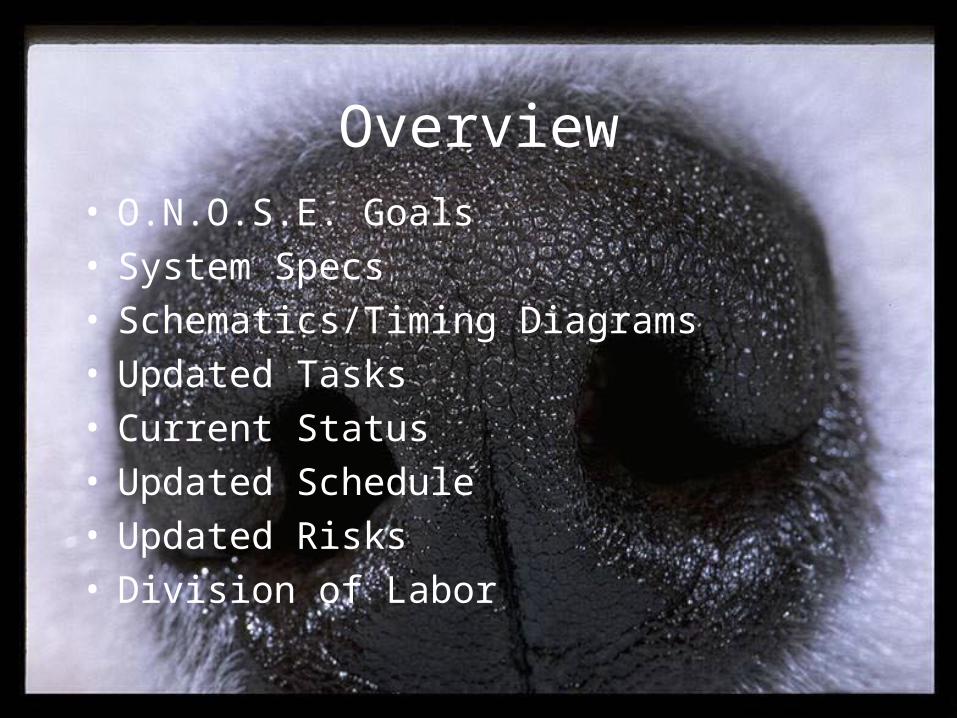
Overview• O.N.O.S.E. Goals• System Specs• Schematics/Timing Diagrams• Updated Tasks• Current Status• Updated Schedule • Updated Risks • Division of Labor
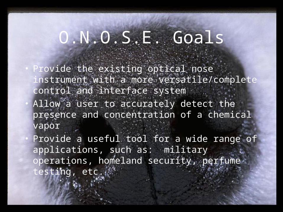
O.N.O.S.E. Goals
• Provide the existing optical nose instrument with a more versatile/complete control and interface system
• Allow a user to accurately detect the presence and concentration of a chemical vapor
• Provide a useful tool for a wide range of applications, such as: military operations, homeland security, perfume testing, etc.
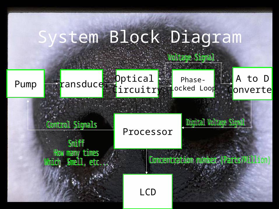
System Block Diagram
Pump TransducerOptical Circuitry
Phase-Locked Loop
A to DConverter
Processor
LCD

System ComponentsClock ECS-2200b 8.0 MHz
Microprocessor MC68HC000
FPGA/PROM Spartan I XCS10/
XC18V256JC
EPROM AM27C512
Data Bus Drivers 74HC245
Address Bus Drivers 74HC244
Resistors/Capacitors Various sizes/values
PLL TBD – analog or digital
A/D and D/A TBD (at least 12-bit)
LCD 2x20 display
Keypad 9 or 12 key

System Schematic – Clock and Reset Circuits
Y1
OSC8
OUT5
U2A
54HC14
1 2
U3B
54HC14
3 4
U4A
54HC14
1 2
U5B
54HC14
3 4
R1100k
C110uF
D1DIODE
SW1SW PUSHBUTTON

System Schematic - Processor
U1
68000/LCC
A132
A233
A334
A435
A536
A637
A738
A839
A940
A1041
A1142
A1243
A1344
A1445
A1546
A1647
A1748
A1849
A1950
A2051
A2153
A2254
A2355
CLK15
D05
D14
D23
D32
D41
D568
D667
D766
D865
D964
D1063
D1162
D1261
D1360
D1459
D1558
FC030
FC129
FC228
AS6
UDS7
LDS8
R/W9
BG11
VMA21
EN22
BERR24
BGACK12
BR13
DTACK10
HALT19
RST20
VPA23
IPL027
IPL126
IPL225
Y1
OSC8
OUT5
U2A
54HC14
1 2
U3B
54HC14
3 4
U4A
54HC14
1 2
U5B
54HC14
3 4
R1100k
C110uF
D1DIODE
SW1SW PUSHBUTTON

Bus Timing - Motorola 68000
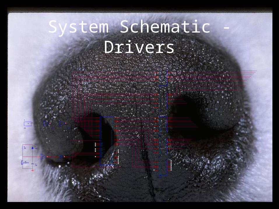
System Schematic - Drivers
U1
68000/LCC
A132
A233
A334
A435
A536
A637
A738
A839
A940
A1041
A1142
A1243
A1344
A1445
A1546
A1647
A1748
A1849
A1950
A2051
A2153
A2254
A2355
CLK15
D05
D14
D23
D32
D41
D568
D667
D766
D865
D964
D1063
D1162
D1261
D1360
D1459
D1558
FC030
FC129
FC228
AS6
UDS7
LDS8
R/W9
BG11
VMA21
EN22
BERR24
BGACK12
BR13
DTACK10
HALT19
RST20
VPA23
IPL027
IPL126
IPL225
Y1
OSC8
OUT5
U2A
54HC14
1 2
U3B
54HC14
3 4
U4A
54HC14
1 2
U5B
54HC14
3 4
R1100k
C110uF
D1DIODE
SW1SW PUSHBUTTON
U6
74LS244
A12
A24
A36
A48
1OE1
Y118
Y216
Y314
Y412
A511
A613
A715
A817
Y59
Y67
Y75
Y83
2OE19
U7
74LS244
A12
A24
A36
A48
1OE1
Y118
Y216
Y314
Y412
A511
A613
A715
A817
Y59
Y67
Y75
Y83
2OE19
U8
74LS244
A12
A24
A36
A48
1OE1
Y118
Y216
Y314
Y412
A511
A613
A715
A817
Y59
Y67
Y75
Y83
2OE19
U9
74LS245
A02
A13
A24
A35
A46
A57
A68
A79
G19 DIR
1
B018
B117
B216
B315
B414
B513
B612
B711
U10
74LS245
A02
A13
A24
A35
A46
A57
A68
A79
G19 DIR
1
B018
B117
B216
B315
B414
B513
B612
B711

Example Pin-outsAddress and Data Drivers

System Schematic - ROM
U1
68000/LCC
A132
A233
A334
A435
A536
A637
A738
A839
A940
A1041
A1142
A1243
A1344
A1445
A1546
A1647
A1748
A1849
A1950
A2051
A2153
A2254
A2355
CLK15
D05
D14
D23
D32
D41
D568
D667
D766
D865
D964
D1063
D1162
D1261
D1360
D1459
D1558
FC030
FC129
FC228
AS6
UDS7
LDS8
R/W9
BG11
VMA21
EN22
BERR24
BGACK12
BR13
DTACK10
HALT19
RST20
VPA23
IPL027
IPL126
IPL225
Y1
OSC8
OUT5
U2A
54HC14
1 2
U3B
54HC14
3 4
U4A
54HC14
1 2
U5B
54HC14
3 4
R1100k
C110uF
D1DIODE
SW1SW PUSHBUTTON
U6
74LS244
A12
A24
A36
A48
1OE1
Y118
Y216
Y314
Y412
A511
A613
A715
A817
Y59
Y67
Y75
Y83
2OE19
U7
74LS244
A12
A24
A36
A48
1OE1
Y118
Y216
Y314
Y412
A511
A613
A715
A817
Y59
Y67
Y75
Y83
2OE19
U8
74LS244
A12
A24
A36
A48
1OE1
Y118
Y216
Y314
Y412
A511
A613
A715
A817
Y59
Y67
Y75
Y83
2OE19
U9
74LS245
A02
A13
A24
A35
A46
A57
A68
A79
G19 DIR
1
B018
B117
B216
B315
B414
B513
B612
B711
U10
74LS245
A02
A13
A24
A35
A46
A57
A68
A79
G19 DIR
1
B018
B117
B216
B315
B414
B513
B612
B711
U11
27C512
A151
A122
A73 A64 A55 A46 A37 A28 A19 A0
10
A1021
A1123
A924 A825
A1427 A1326
O011
O112
O213
O315
O416
O517
O618
O719
CE20 OE/VPP22
U12
27C512
A151
A122
A73 A64 A55 A46 A37 A28 A19 A0
10
A1021
A1123
A924 A825
A1427 A1326
O011
O112
O213
O315
O416
O517
O618
O719
CE20 OE/VPP22
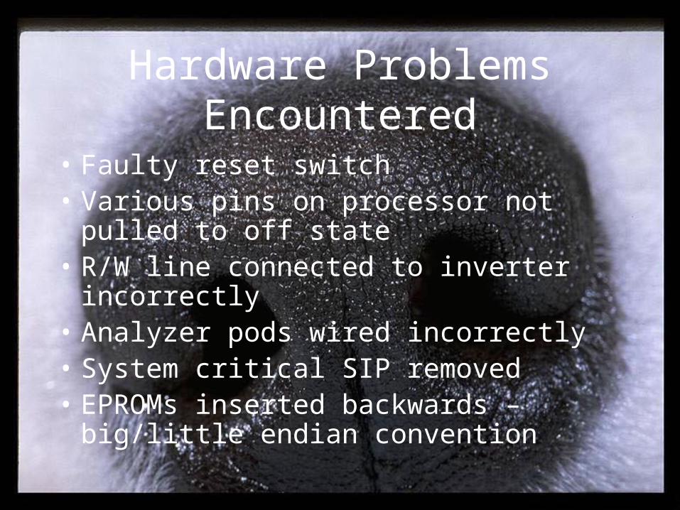
Hardware Problems Encountered
• Faulty reset switch• Various pins on processor not pulled to off
state• R/W line connected to inverter incorrectly• Analyzer pods wired incorrectly• System critical SIP removed• EPROMs inserted backwards – big/little
endian convention

Detailed Tasks
• Ever-present Tasks
• Processor Hardware
• Software
• Interfacing
• Functional Definition
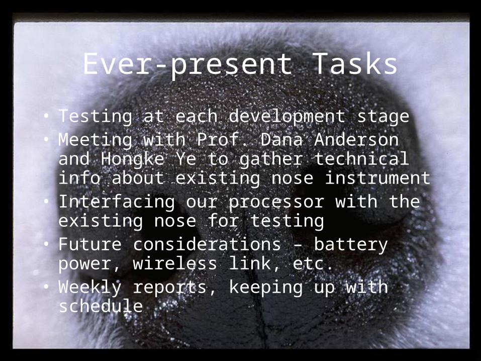
Ever-present Tasks
• Testing at each development stage• Meeting with Prof. Dana Anderson and Hongke
Ye to gather technical info about existing nose instrument
• Interfacing our processor with the existing nose for testing
• Future considerations – battery power, wireless link, etc.
• Weekly reports, keeping up with schedule

Processor Hardware Tasks
• Reset Circuit
• Clock
• Bypass Caps
• Processor
• Bus Drivers/Pull-ups
• ROM (test nop-nop-nop-jmp at this point)
• FPGA/PROM
• JTAG Interface
• RAM• RAM walkthrough test• (DIP switch/LEDs for
testing)• Serial Port• A/Ds and D/As• Phase-Locked Loop• LCD• Keypad• More components TBD
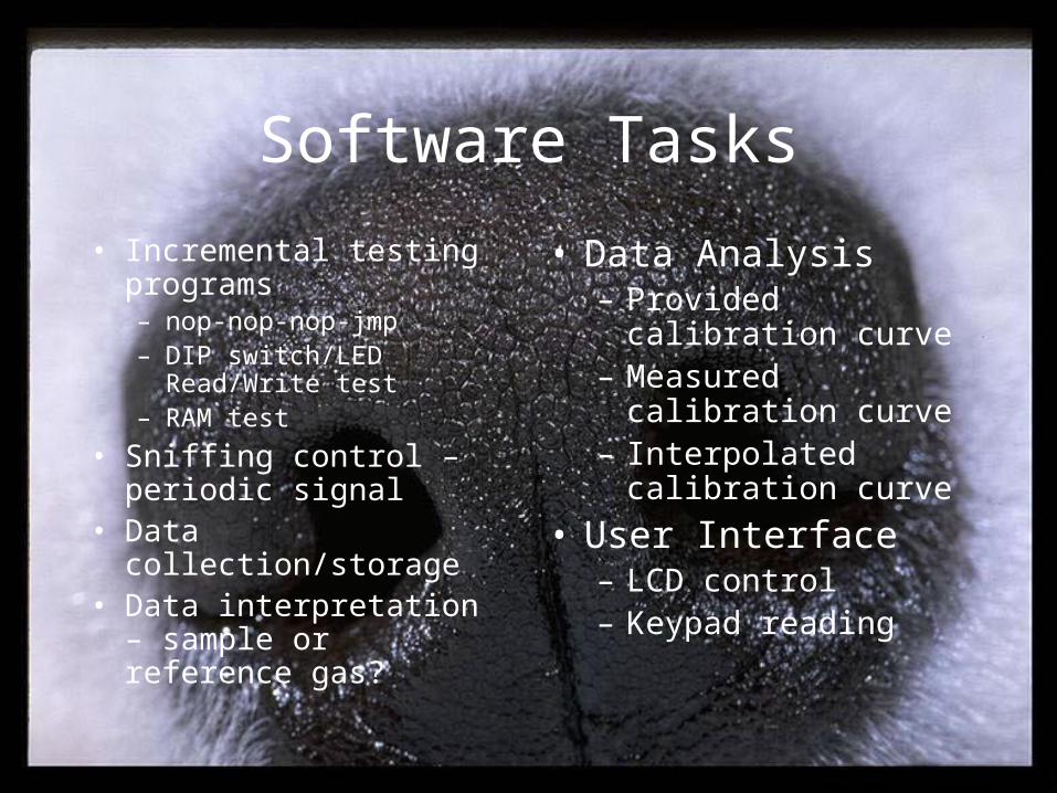
Software Tasks
• Incremental testing programs– nop-nop-nop-jmp– DIP switch/LED
Read/Write test– RAM test
• Sniffing control – periodic signal
• Data collection/storage• Data interpretation –
sample or reference gas?
• Data Analysis– Provided calibration
curve– Measured calibration
curve– Interpolated calibration
curve
• User Interface– LCD control– Keypad reading

Interfacing Tasks
• Gas pump control – periodic signal– Signal characteristics– Chemistry/physics limitations
or concerns– How to process the
reference/sample gas signals
• Synchronization– Phase-locked loop to keep
detector signal in sync with the pump control
– Analog or Digital?– Implementation
• Calibration Curve– Lookup table
– Interpolation – how?
• User Interface– Keys/buttons
– LCD
– Serial output to PC – data file creation – plotting, etc.

Functional Definition
• Get a solid idea of what the device should do– Purpose
– Applications
• Come up with or find out concrete specifications for inputs/outputs and how to process/interface them
• Determine or assume how the user will want to interact with the device
• Get everyone on the same page for the rest of the development process!

Current Status
• Processor wire wrapped and tested
• Reset and Clock circuits Functioning
• Address and Data Drivers wire wrapped
• EPROM wire wrapped
• NOP-NOP-NOP-JMP Executed from ROM
• Prepared to implement the FPGA
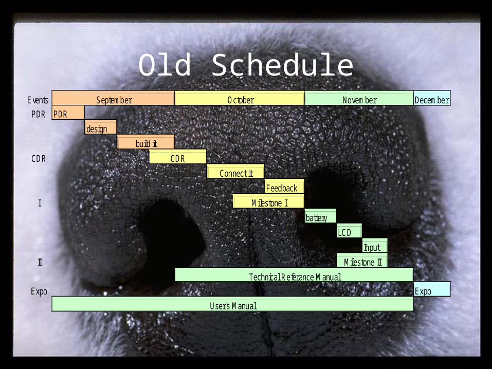
Old ScheduleEvents September October November December
PDR PDR
design
build it
CDR CDR
Connect it
Feedback
I Milestone I
battery
LCD
Input
II Milestone II
Technical Referance Manual
Expo Expo
User's Manual
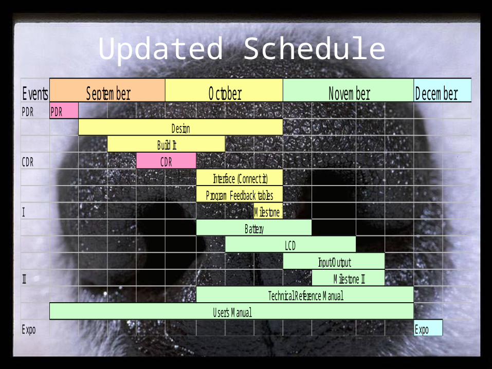
Updated ScheduleEvents DecemberPDR PDR
CDR
I Milestone I
II
Expo Expo
September October November
DesignBuild It
CDRInterface (Connect it)
Milestone IITechnical Reference Manual
User's Manual
Program Feedback tables
BatteryLCD
Input/Output
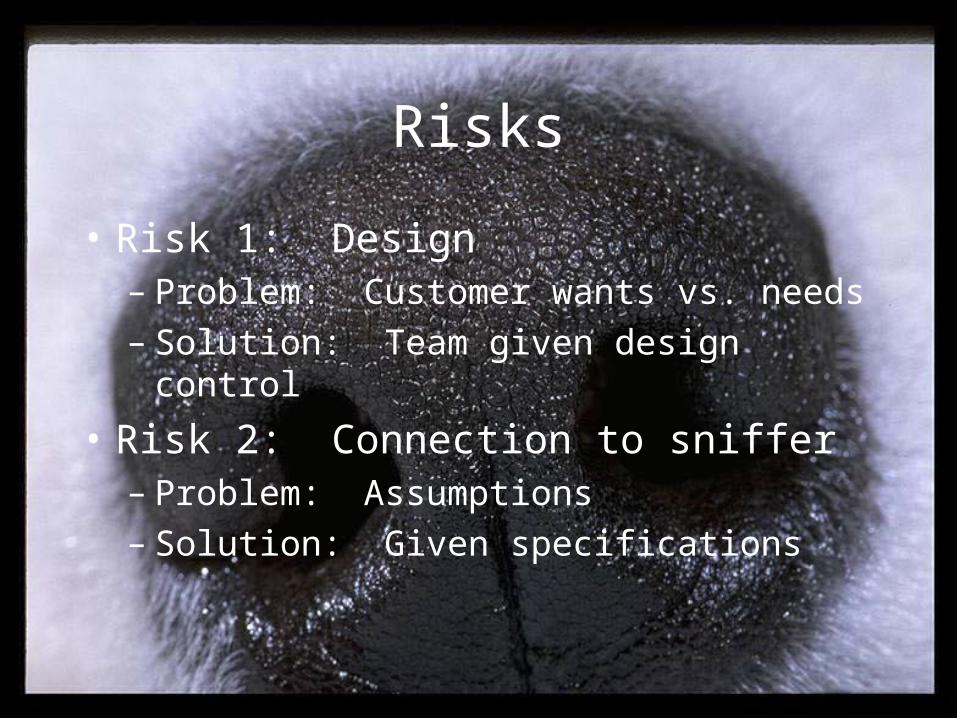
Risks
• Risk 1: Design– Problem: Customer wants vs. needs– Solution: Team given design control
• Risk 2: Connection to sniffer– Problem: Assumptions – Solution: Given specifications

Risks Cont.
• Risk 3: Feedback– Problem: unknown PPM– Solution1: Given equations for feedback curve– Solution2: Access to known concentrations
• Risk 4: Battery Power– Problem: lack of experience with Battery power
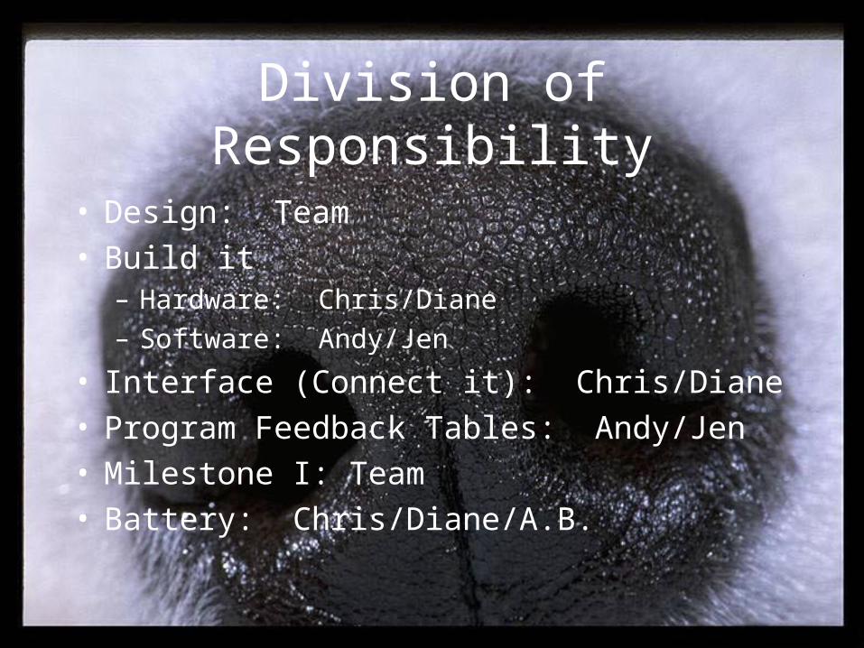
Division of Responsibility
• Design: Team• Build it
– Hardware: Chris/Diane
– Software: Andy/Jen
• Interface (Connect it): Chris/Diane• Program Feedback Tables: Andy/Jen• Milestone I: Team• Battery: Chris/Diane/A.B.

Division of Responsibility cont.
• LCD: A.B./Andy/Jen
• PLL: A.B./Andy
• Input/Output: Team
• Milestone II: Team
• Tech. Reference Manual: A.B./Team
• User’s Manual: A.B./Team
• Research: Team

Costs So Far
• Wire Wrap Board: $ 11.83
• Power Leads and Stand-offs: $ 3.66
• Capacitor: $0.43
• Total: $15.92

Questions?
• Jennifer – Overview, System Block Diagram
• A.B. – System Specs
• Chris – Hardware problems and tasks
• Andy – Software and Interfacing tasks
• Diane – Schedule, risks and division of labor