PROJECT #2 SPACE VECTOR PWM INVERTER - Read
35
PROJECT #2 SPACE VECTOR PWM INVERTER JIN-WOO JUNG, PH.D STUDENT E-mail: [email protected] Tel.: (614) 292-3633 ADVISOR: PROF. ALI KEYHANI DATE: FEBRUARY 20, 2005 MECHATRONIC SYSTEMS LABORATORY DEPARTMENT OF ELECTRICAL AND COMPUTER ENGINEERING THE OHIO STATE UNIVERSITY
Transcript of PROJECT #2 SPACE VECTOR PWM INVERTER - Read

PROJECT #2 SPACE VECTOR PWM INVERTER
JIN-WOO JUNG, PH.D STUDENT E-mail: [email protected]
Tel.: (614) 292-3633
ADVISOR: PROF. ALI KEYHANI
DATE: FEBRUARY 20, 2005
MECHATRONIC SYSTEMS LABORATORY
DEPARTMENT OF ELECTRICAL AND COMPUTER ENGINEERING
THE OHIO STATE UNIVERSITY

2
1. Problem Description
In this simulation, we will study Space Vector Pulse Width Modulation (SVPWM) technique.
We will use the SEMIKRON® IGBT Flexible Power Converter for this purpose. The system
configuration is given below:
Fig. 1 Circuit model of three-phase PWM inverter with a center-taped grounded DC bus.
The system parameters for this converter are as follows:
IGBTs: SEMIKRON SKM 50 GB 123D, Max ratings: VCES = 600 V, IC = 80 A
DC- link voltage: Vdc = 400 V
Fundamental frequency: f = 60 Hz
PWM (carrier) frequency: fz = 3 kHz
Modulation index: a = 0.6
Output filter: Lf = 800 µH and Cf = 400 µF
Load: Lload = 2 mH and Rload = 5 Ω
Using Matlab/Simulink, simulate the circuit model described in Fig. 1 and plot the
waveforms of Vi (= [ViAB ViBC ViCA]), Ii (= [iiA iiB iiC]), VL (= [VLAB VLBC VLCA]), and IL (= [iLA
iLB iLC]).

3
2. Space Vector PWM
2.1 Principle of Pulse Width Modulation (PWM)
Fig. 2 shows circuit model of a single-phase inverter with a center-taped grounded DC bus,
and Fig 3 illustrates principle of pulse width modulation.
Fig. 2 Circuit model of a single-phase inverter.
Fig. 3 Pulse width modulation.
As depicted in Fig. 3, the inverter output voltage is determined in the following:
When Vcontrol > Vtri, VA0 = Vdc/2
When Vcontrol < Vtri, VA0 = −Vdc/2

4
Also, the inverter output voltage has the following features:
PWM frequency is the same as the frequency of Vtri
Amplitude is controlled by the peak value of Vcontrol
Fundamental frequency is controlled by the frequency of Vcontrol
Modulation index (m) is defined as:
A01A0
10
Vofcomponentfrequecnylfundamenta:)(Vwhere,
,2/
)(
dc
A
tri
control
VVofpeak
vv
m ==∴
2.2 Principle of Space Vector PWM
The circuit model of a typical three-phase voltage source PWM inverter is shown in Fig. 4.
S1 to S6 are the six power switches that shape the output, which are controlled by the switching
variables a, a′, b, b′, c and c′. When an upper transistor is switched on, i.e., when a, b or c is 1,
the corresponding lower transistor is switched off, i.e., the corresponding a′, b′ or c′ is 0.
Therefore, the on and off states of the upper transistors S1, S3 and S5 can be used to determine the
output voltage.
Fig. 4 Three-phase voltage source PWM Inverter.

5
The relationship between the switching variable vector [a, b, c]t and the line-to-line voltage
vector [Vab Vbc Vca]t is given by (2.1) in the following:
⎥⎥⎥
⎦
⎤
⎢⎢⎢
⎣
⎡
⎥⎥⎥
⎦
⎤
⎢⎢⎢
⎣
⎡
−−
−=
⎥⎥⎥
⎦
⎤
⎢⎢⎢
⎣
⎡
cba
VVVV
dc
ca
bc
ab
101110
011. (2.1)
Also, the relationship between the switching variable vector [a, b, c]t and the phase voltage
vector [Va Vb Vc]t can be expressed below.
⎥⎥⎥
⎦
⎤
⎢⎢⎢
⎣
⎡
⎥⎥⎥
⎦
⎤
⎢⎢⎢
⎣
⎡
−−−−−−
=⎥⎥⎥
⎦
⎤
⎢⎢⎢
⎣
⎡
cba
V
VVV
dc
cn
bn
an
211121112
3. (2.2)
As illustrated in Fig. 4, there are eight possible combinations of on and off patterns for the
three upper power switches. The on and off states of the lower power devices are opposite to the
upper one and so are easily determined once the states of the upper power transistors are
determined. According to equations (2.1) and (2.2), the eight switching vectors, output line to
neutral voltage (phase voltage), and output line-to-line voltages in terms of DC-link Vdc, are
given in Table1 and Fig. 5 shows the eight inverter voltage vectors (V0 to V7).
Table 1. Switching vectors, phase voltages and output line to line voltages

6
Fig. 5 The eight inverter voltage vectors (V0 to V7).
Space Vector PWM (SVPWM) refers to a special switching sequence of the upper three
power transistors of a three-phase power inverter. It has been shown to generate less harmonic
distortion in the output voltages and or currents applied to the phases of an AC motor and to

7
provide more efficient use of supply voltage compared with sinusoidal modulation technique as
shown in Fig. 6.
Fig. 6 Locus comparison of maximum linear control voltage in Sine PWM and SVPWM.
To implement the space vector PWM, the voltage equations in the abc reference frame
can be transformed into the stationary dq reference frame that consists of the horizontal (d) and
vertical (q) axes as depicted in Fig. 7.
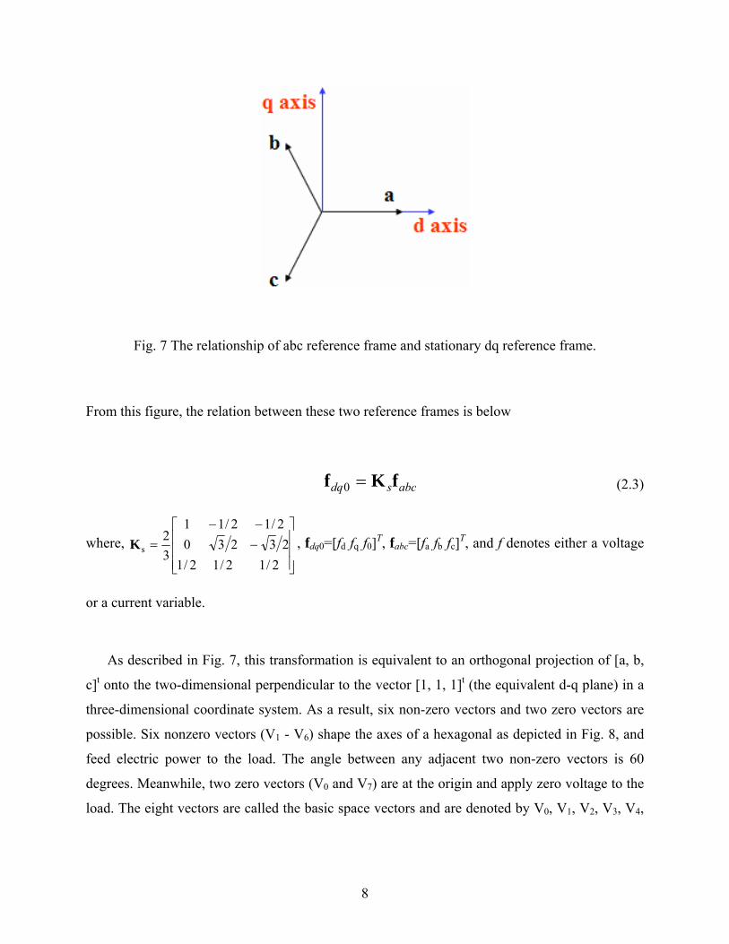
8
Fig. 7 The relationship of abc reference frame and stationary dq reference frame.
From this figure, the relation between these two reference frames is below
abcsdq fKf =0 (2.3)
where, ⎥⎥⎥
⎦
⎤
⎢⎢⎢
⎣
⎡−−−
=2/12/12/1
232302/12/11
32
sK , fdq0=[fd fq f0]T, fabc=[fa fb fc]T, and f denotes either a voltage
or a current variable.
As described in Fig. 7, this transformation is equivalent to an orthogonal projection of [a, b,
c]t onto the two-dimensional perpendicular to the vector [1, 1, 1]t (the equivalent d-q plane) in a
three-dimensional coordinate system. As a result, six non-zero vectors and two zero vectors are
possible. Six nonzero vectors (V1 - V6) shape the axes of a hexagonal as depicted in Fig. 8, and
feed electric power to the load. The angle between any adjacent two non-zero vectors is 60
degrees. Meanwhile, two zero vectors (V0 and V7) are at the origin and apply zero voltage to the
load. The eight vectors are called the basic space vectors and are denoted by V0, V1, V2, V3, V4,

9
V5, V6, and V7. The same transformation can be applied to the desired output voltage to get the
desired reference voltage vector Vref in the d-q plane.
The objective of space vector PWM technique is to approximate the reference voltage vector
Vref using the eight switching patterns. One simple method of approximation is to generate the
average output of the inverter in a small period, T to be the same as that of Vref in the same
period.
Fig. 8 Basic switching vectors and sectors.
Therefore, space vector PWM can be implemented by the following steps:
Step 1. Determine Vd, Vq, Vref, and angle (α)
Step 2. Determine time duration T1, T2, T0
Step 3. Determine the switching time of each transistor (S1 to S6)
2.2.1 Step 1: Determine Vd, Vq, Vref, and angle (α)
From Fig. 9, the Vd, Vq, Vref, and angle (α) can be determined as follows:

10
cnbnan
cnbnand
V21V
21V
cos60Vcos60VVV
−−=
⋅−⋅−=
cnbnan
cnbnq
V23V
23V
cos30Vcos30V0V
−+=
⋅−⋅+=
⎥⎥⎥
⎦
⎤
⎢⎢⎢
⎣
⎡
⎥⎥⎥⎥
⎦
⎤
⎢⎢⎢⎢
⎣
⎡
−
−−=⎥
⎦
⎤⎢⎣
⎡∴
cn
bn
an
q
d
VVV
VV
23
230
21
211
32
22qdref VVV +=∴
frequency lfundamenta f where,2tan 1 ===⎟⎟⎠
⎞⎜⎜⎝
⎛=∴ − ftt
VV
d
q πωα
Fig. 9 Voltage Space Vector and its components in (d, q).
2.2.2 Step 2: Determine time duration T1, T2, T0
From Fig. 10, the switching time duration can be calculated as follows:

11
Switching time duration at Sector 1
)60α0(where,)3/(sin)3/(cos
V32T
01
V32T
)(sin)(cos
VT
)VTV(TVT
VdtVdtVV
dc2dc1refz
2211refz
zT
2T1T0
2T1T
T12
zT
0
1T
01ref
°≤≤
⎥⎦
⎤⎢⎣
⎡⋅⋅⋅+⎥
⎦
⎤⎢⎣
⎡⋅⋅⋅=⎥
⎦
⎤⎢⎣
⎡⋅⋅⇒
⋅+⋅=⋅∴
++= ∫∫∫ ∫+
+
ππ
αα
⎟⎟⎟⎟
⎠
⎞
⎜⎜⎜⎜
⎝
⎛
==+−=∴
⋅⋅=∴
−⋅⋅=∴
dc
ref
zz210
2
1
V32V
aandf1Twhere,),(
)3/(sin)(sin
)3/(sin)3/(sin
TTTT
aTT
aTT
z
z
z
παπ
απ
Switching time duration at any Sector
⎟⎟⎠
⎞⎜⎜⎝
⎛°≤≤
=−−=∴
⎟⎠⎞
⎜⎝⎛ −
⋅+−
⋅−⋅
=
⎟⎟⎠
⎞⎜⎜⎝
⎛⎟⎠⎞
⎜⎝⎛ −
−⋅⋅
=∴
⎟⎠⎞
⎜⎝⎛ −
⋅⋅=
⎟⎠⎞
⎜⎝⎛ −
⋅⋅=
⎟⎟⎠
⎞⎜⎜⎝
⎛⎟⎠⎞
⎜⎝⎛ −
+−⋅⋅
=∴
60α06)toSector1is,(that6through1nwhere,
,
31cossin
31sincos
3
31sin
3
sin3
coscos3
sin3
3sin
3
31
3sin
3
210
2
1
TTTT
nnV
refVT
nV
refVTT
nnV
refVT
nV
refVT
nV
refVTT
z
dc
z
dc
z
dc
z
dc
z
dc
z
παπα
πα
απαπ
απ
παπ

12
Fig. 10 Reference vector as a combination of adjacent vectors at sector 1.
2.2.3 Step 3: Determine the switching time of each transistor (S1 to S6)
Fig. 11 shows space vector PWM switching patterns at each sector.
(a) Sector 1. (b) Sector 2.

13
(c) Sector 3. (d) Sector 4.
(e) Sector 5. (f) Sector 6.
Fig. 11 Space Vector PWM switching patterns at each sector.
Based on Fig. 11, the switching time at each sector is summarized in Table 2, and it will be
built in Simulink model to implement SVPWM.

14
Table 2. Switching Time Calculation at Each Sector

15
3. State-Space Model
Fig. 12 shows L-C output filter to obtain current and voltage equations.
Fig. 12 L-C output filter for current/voltage equations.
By applying Kirchoff’s current law to nodes a, b, and c, respectively, the following current
equations are derived:
node “a”:
LALAB
fLCA
fiALAabcaiA idt
dVC
dtdV
Ciiiii +=+⇒+=+ . (3.1)
node “b”:
LBLBC
fLAB
fiBLBbcabiB idt
dVC
dtdV
Ciiiii +=+⇒+=+ . (3.2)
node “c”:

16
LCLCA
fLBC
fiCLCcabciC idt
dVC
dtdV
Ciiiii +=+⇒+=+ . (3.2)
where, .,,dt
dVCi
dtdV
Cidt
dVCi LCAfca
LBCfbc
LABfab ===
Also, (3.1) to (3.3) can be rewritten as the following equations, respectively:
subtracting (3.2) from (3.1):
LBLAiBiALABLBCLCA
f
LBLALBCLAB
fLABLCA
fiBiA
iiiidt
dVdt
dVdt
dVC
iidt
dVdt
dVC
dtdV
dtdV
Cii
−++−=⎟⎠
⎞⎜⎝
⎛ ⋅−+⇒
−+⎟⎠
⎞⎜⎝
⎛ −=⎟⎠
⎞⎜⎝
⎛ −+−
2
. (3.4)
subtracting (3.3) from (3.2):
LCLBiCiBLBCLCALAB
f
LCLBLCALBC
fLBCLAB
fiCiB
iiiidt
dVdt
dVdt
dVC
iidt
dVdt
dVC
dtdV
dtdV
Cii
−++−=⎟⎠
⎞⎜⎝
⎛ ⋅−+⇒
−+⎟⎠
⎞⎜⎝
⎛ −=⎟⎠
⎞⎜⎝
⎛ −+−
2
. (3.5)
subtracting (3.1) from (3.3):
LALCiAiCLCALBCLAB
f
LALCLABLCA
fLCALBC
fiAiC
iiiidt
dVdt
dVdt
dVC
iidt
dVdt
dVC
dtdV
dtdV
Cii
−++−=⎟⎠
⎞⎜⎝
⎛ ⋅−+⇒
−+⎟⎠
⎞⎜⎝
⎛ −=⎟⎠
⎞⎜⎝
⎛ −+−
2
. (3.6)
To simplify (3.4) to (3.6), we use the following relationship that an algebraic sum of line to line
load voltages is equal to zero:
VLAB + VLBC + VLCA = 0. (3.7)

17
Based on (3.7), the (3.4) to (3.6) can be modified to a first-order differential equation,
respectively:
( )
( )
( )⎪⎪⎪
⎩
⎪⎪⎪
⎨
⎧
−=
−=
−=
LCAf
iCAf
LCA
CLBf
iBCf
LBC
LABf
iABf
LAB
iC
iCdt
dV
iC
iCdt
dV
iC
iCdt
dV
31
31
31
31
31
31
, (3.8)
where, iiAB = iiA iiB, iiBC = iiB iiC, iiCA
= iiC iiA and iLAB = iLA iLB, iLBC = iLB iLC,
iLCA = iLC iLA.
By applying Kirchoff’s voltage law on the side of inverter output, the following voltage
equations can be derived:
⎪⎪⎪
⎩
⎪⎪⎪
⎨
⎧
+−=
+−=
+−=
iCAf
LCAf
iCA
iBCf
LBCf
iBC
iABf
LABf
iAB
VL
VLdt
di
VL
VLdt
di
VL
VLdt
di
11
11
11
. (3.9)
By applying Kirchoff’s voltage law on the load side, the following voltage equations can be
derived:
⎪⎪⎪
⎩
⎪⎪⎪
⎨
⎧
−−+=
−−+=
−−+=
LAloadLA
loadLCloadLC
loadLCA
LCloadLC
loadLBloadLB
loadLBC
LBloadLB
loadLAloadLA
loadLAB
iRdt
diLiR
dtdi
LV
iRdt
diLiR
dtdi
LV
iRdt
diLiR
dtdi
LV
. (3.10)

18
Equation (3.10) can be rewritten as:
⎪⎪⎪⎪
⎩
⎪⎪⎪⎪
⎨
⎧
+−=
+−=
+−=
LCAload
LCAload
loadLCA
LBCload
LBCload
loadLBC
LABload
LABload
loadLAB
VL
iLR
dtdi
VL
iLR
dtdi
VL
iLR
dtdi
1
1
1
. (3.11)
Therefore, we can rewrite (3.8), (3.9) and (3.11) into a matrix form, respectively:
Lload
loadL
load
L
if
Lf
i
Lf
if
L
LR
Ldtd
LLdtd
CCdtd
IVI
VVI
IIV
−=
+−=
−=
1
11
31
31
, (3.12)
where, VL = [VLAB VLBC VLCA]T , Ii = [iiAB iiBC iiCA]T = [iiA-iiB iiB-iiC iiC-iiA]T , Vi = [ViAB ViBC ViCA]T ,
IL = = [iLAB iLBC iLCA]T = [iLA-iLB iLB-iLC iLC-iLA]T.
Finally, the given plant model (3.12) can be expressed as the following continuous-time state
space equation
)()()( ttt BuAXX +=& , (3.13)
where,
19×⎥⎥⎥
⎦
⎤
⎢⎢⎢
⎣
⎡=
L
i
L
IIV
X ,
99333333
333333
333333
01
0013
13
10
××××
×××
×××
⎥⎥⎥⎥⎥⎥⎥
⎦
⎤
⎢⎢⎢⎢⎢⎢⎢
⎣
⎡
−
−
−
=
ILR
IL
IL
IC
IC
load
load
load
f
ff
A ,
3933
33
33
0
10
××
×
×
⎥⎥⎥⎥
⎦
⎤
⎢⎢⎢⎢
⎣
⎡
= IL f
B , [ ] 13×= iVu .

19
Note that load line to line voltage VL, inverter output current Ii, and the load current IL are the
state variables of the system, and the inverter output line-to-line voltage Vi is the control input
(u).
4. Simulation Steps
1). Initialize system parameters using Matlab
2). Build Simulink Model
Determine sector
Determine time duration T1, T2, T0
Determine the switching time (Ta, Tb, and Tc) of each transistor (S1 to S6)
Generate the inverter output voltages (ViAB, ViBC, ViCA,) for control input (u)
Send data to Workspace
3). Plot simulation results using Matlab

20
5. Simulation results
0.9 0.91 0.92 0.93 0.94 0.95 0.96 0.97 0.98 0.99 1-500
0
500
ViA
B [V
]
Inverter output line to line voltages (ViAB, ViBC, ViCA)
0.9 0.91 0.92 0.93 0.94 0.95 0.96 0.97 0.98 0.99 1-500
0
500
ViB
C [V
]
0.9 0.91 0.92 0.93 0.94 0.95 0.96 0.97 0.98 0.99 1-500
0
500
ViC
A [V
]
Time [Sec]
Fig. 13 Simulation results of inverter output line to line voltages (ViAB, ViBC, ViCA)

21
0.9 0.91 0.92 0.93 0.94 0.95 0.96 0.97 0.98 0.99 1-100
-50
0
50
100i iA
[A]
Inverter output currents (iiA, iiB, iiC)
0.9 0.91 0.92 0.93 0.94 0.95 0.96 0.97 0.98 0.99 1-100
-50
0
50
100
i iB [A
]
0.9 0.91 0.92 0.93 0.94 0.95 0.96 0.97 0.98 0.99 1-100
-50
0
50
100
i iC [A
]
Time [Sec]
Fig. 14 Simulation results of inverter output currents (iiA, iiB, iiC)

22
0.9 0.91 0.92 0.93 0.94 0.95 0.96 0.97 0.98 0.99 1-400
-200
0
200
400V
LAB
[V]
Load line to line voltages (VLAB, VLBC, VLCA)
0.9 0.91 0.92 0.93 0.94 0.95 0.96 0.97 0.98 0.99 1-400
-200
0
200
400
VLB
C [V
]
0.9 0.91 0.92 0.93 0.94 0.95 0.96 0.97 0.98 0.99 1-400
-200
0
200
400
VLC
A [V
]
Time [Sec]
Fig. 15 Simulation results of load line to line voltages (VLAB, VLBC, VLCA)

23
0.9 0.91 0.92 0.93 0.94 0.95 0.96 0.97 0.98 0.99 1-50
0
50i LA
[A]
Load phase currents (iLA, iLB, iLC)
0.9 0.91 0.92 0.93 0.94 0.95 0.96 0.97 0.98 0.99 1-50
0
50
i LB [A
]
0.9 0.91 0.92 0.93 0.94 0.95 0.96 0.97 0.98 0.99 1-50
0
50
i LC [A
]
Time [Sec]
Fig. 16 Simulation results of load phase currents (iLA, iLB, iLC)

24
0.9 0.91 0.92 0.93 0.94 0.95 0.96 0.97 0.98 0.99 1-500
0
500V
iAB
[V]
0.9 0.91 0.92 0.93 0.94 0.95 0.96 0.97 0.98 0.99 1-100
0
100
i iA, i
iB, i
iC [A
] iiAiiBiiC
0.9 0.91 0.92 0.93 0.94 0.95 0.96 0.97 0.98 0.99 1-400
-200
0
200
400
VLA
B, V
LBC,
VLC
A [V
]
VLABVLBCVLCA
0.9 0.91 0.92 0.93 0.94 0.95 0.96 0.97 0.98 0.99 1-50
0
50
i LA, i
LB, i
LC [A
]
Time [Sec]
iLAiLBiLC
Fig. 17 Simulation waveforms.
(a) Inverter output line to line voltage (ViAB)
(b) Inverter output current (iiA)
(c) Load line to line voltage (VLAB)
(d) Load phase current (iLA)

25
Appendix
Matlab/Simulink Codes

26
A.1 Matlab Code for System Parameters
% Written by Jin Woo Jung
% Date: 02/20/05
% ECE743, Simulation Project #2 (Space Vector PWM Inverter)
% Matlab program for Parameter Initialization
clear all % clear workspace
% Input data
Vdc= 400; % DC-link voltage
Lf= 800e-6;% Inductance for output filter
Cf= 400e-6; % Capacitance for output filter
Lload = 2e-3; %Load inductance
Rload= 5; % Load resistance
f= 60; % Fundamental frequency
fz = 3e3; % Switching frequency
a= 0.6;% Modulation index
w= 2*pi*60; %angular frequency
Tz= 1/fz; % Sampling time
V_ref= (2/3)*a*Vdc; % Reference voltage
% Coefficients for State-Space Model
A=[zeros(3,3) eye(3)/(3*Cf) -eye(3)/(3*Cf)
-eye(3)/Lf zeros(3,3) zeros(3,3)
eye(3,3)/Lload zeros(3,3) -eye(3)*Rload/Lload]; % system matrix
B=[zeros(3,3)
eye(3)/Lf
zeros(3,3)]; % coefficient for the control variable u

27
C=[eye(9)]; % coefficient for the output y
D=[zeros(9,3)]; % coefficient for the output y
Ks = 1/3*[-1 0 1; 1 -1 0; 0 1 -1]; % Conversion matrix to transform [iiAB iiBC iiCA] to [iiA iiB
iiC]

28
A.2 Matlab Code for Plotting the Simulation Results
% Written by Jin Woo Jung
% Date: 02/20/05
% ECE743, Simulation Project #2 (Space Vector PWM)
% Matlab program for plotting Simulation Results
% using Simulink
ViAB = Vi(:,1);
ViBC = Vi(:,2);
ViCA = Vi(:,3);
VLAB= VL(:,1);
VLBC= VL(:,2);
VLCA= VL(:,3);
iiA= IiABC(:,1);
iiB= IiABC(:,2);
iiC= IiABC(:,3);
iLA= ILABC(:,1);
iLB= ILABC(:,2);
iLC= ILABC(:,3);
figure(1)
subplot(3,1,1)
plot(t,ViAB)
axis([0.9 1 -500 500])
ylabel('V_i_A_B [V]')
title('Inverter output line to line voltages (V_i_A_B, V_i_B_C, V_i_C_A)')

29
grid
subplot(3,1,2)
plot(t,ViBC)
axis([0.9 1 -500 500])
ylabel('V_i_B_C [V]')
grid
subplot(3,1,3)
plot(t,ViCA)
axis([0.9 1 -500 500])
ylabel('V_i_C_A [V]')
xlabel('Time [Sec]')
grid
figure(2)
subplot(3,1,1)
plot(t,iiA)
axis([0.9 1 -100 100])
ylabel('i_i_A [A]')
title('Inverter output currents (i_i_A, i_i_B, i_i_C)')
grid
subplot(3,1,2)
plot(t,iiB)
axis([0.9 1 -100 100])
ylabel('i_i_B [A]')
grid
subplot(3,1,3)

30
plot(t,iiC)
axis([0.9 1 -100 100])
ylabel('i_i_C [A]')
xlabel('Time [Sec]')
grid
figure(3)
subplot(3,1,1)
plot(t,VLAB)
axis([0.9 1 -400 400])
ylabel('V_L_A_B [V]')
title('Load line to line voltages (V_L_A_B, V_L_B_C, V_L_C_A)')
grid
subplot(3,1,2)
plot(t,VLBC)
axis([0.9 1 -400 400])
ylabel('V_L_B_C [V]')
grid
subplot(3,1,3)
plot(t,VLCA)
axis([0.9 1 -400 400])
ylabel('V_L_C_A [V]')
xlabel('Time [Sec]')
grid
figure(4)
subplot(3,1,1)
plot(t,iLA)
axis([0.9 1 -50 50])
31
ylabel('i_L_A [A]')
title('Load phase currents (i_L_A, i_L_B, i_L_C)')
grid
subplot(3,1,2)
plot(t,iLB)
axis([0.9 1 -50 50])
ylabel('i_L_B [A]')
grid
subplot(3,1,3)
plot(t,iLC)
axis([0.9 1 -50 50])
ylabel('i_L_C [A]')
xlabel('Time [Sec]')
grid
figure(5)
subplot(4,1,1)
plot(t,ViAB)
axis([0.9 1 -500 500])
ylabel('V_i_A_B [V]')
grid
subplot(4,1,2)
plot(t,iiA,'-', t,iiB,'-.',t,iiC,':')
axis([0.9 1 -100 100])
ylabel('i_i_A, i_i_B, i_i_C [A]')
legend('i_i_A', 'i_i_B', 'i_i_C')
grid

32
subplot(4,1,3)
plot(t,VLAB,'-', t,VLBC,'-.',t,VLCA,':')
axis([0.9 1 -400 400])
ylabel('V_L_A_B, V_L_B_C, V_L_C_A [V]')
legend('V_L_A_B', 'V_L_B_C', 'V_L_C_A')
grid
subplot(4,1,4)
plot(t,iLA,'-', t,iLB,'-.',t,iLC,':')
axis([0.9 1 -50 50])
ylabel('i_L_A, i_L_B, i_L_C [A]')
legend('i_L_A', 'i_L_B', 'i_L_C')
xlabel('Time [Sec]')
grid

33
A.3 Simulink Code
Simulink Model for Overall System

34
Subsystem Simulink Model for “Space Vector PWM Generator”

35
Subsystem Simulink Model for “Making Switching Time”
1). T1 = u[1]*(sin(u[3]*pi/3)*cos(u[2])-cos(u[3]*pi/3)*sin(u[2]))
2). T2 = u[1]*(cos((u[3]-1)*(pi/3))*sin(u[2])-sin((u[3]-1)*(pi/3))*cos(u[2]))
3). Ta = (u[4]==1)*(u[1]+u[2]+u[3])+(u[4]==2)*(u[1]+u[2]+u[3]) + (u[4]==3)*(u[1]+u[3]) +
(u[4]==4)*(u[1])+ (u[4]==5)*(u[1])+ (u[4]==6)*(u[1]+u[2])
4). Tb = (u[4]==1)*(u[1])+(u[4]==2)*(u[1]+u[2]) + (u[4]==3)*(u[1]+u[2]+u[3]) +
(u[4]==4)*(u[1]+u[2]+u[3])+ (u[4]==5)*(u[1]+u[3])+ (u[4]==6)*(u[1])
5). Tc = (u[4]==1)*(u[1]+u[3])+(u[4]==2)*(u[1]) + (u[4]==3)*(u[1]) + (u[4]==4)*(u[1]+u[2])+
(u[4]==5)*(u[1]+u[2]+u[3])+ (u[4]==6)*(u[1]+u[2]+u[3])