Prof.P. Ravindran, - Universitetet i...
36
P.Ravindran, PHY02E – Semiconductor Physics, January 2014: Band Formation & direct and indirect gaps -II http://folk.uio.no/ravi/semi2013 Prof.P. Ravindran, Department of Physics, Central University of Tamil Nadu, India Semiconductors – Band Formation & direct and indirect gaps -II 1
Transcript of Prof.P. Ravindran, - Universitetet i...

P.Ravindran, PHY02E – Semiconductor Physics, January 2014: Band Formation & direct and indirect gaps -II
http://folk.uio.no/ravi/semi2013
Prof.P. Ravindran, Department of Physics, Central University of Tamil
Nadu, India
Semiconductors – Band Formation & direct and
indirect gaps -II
1

P.Ravindran, PHY02E – Semiconductor Physics, January 2014: Band Formation & direct and indirect gaps -II
Energy Levels
a
An Atom
Ener
gy
E = 0
a
A Small
Molecule
a
A Large
Molecule
Filled
States
Empty
States
HOMO
LUMO
Fermi
Level
Vacuum
Level
Chemistry is controlled by the states around the filled/empty transition.
Bulk
Material

P.Ravindran, PHY02E – Semiconductor Physics, January 2014: Band Formation & direct and indirect gaps -II
Band Structure
Metal
Core
Bands
Valence
Band
overlap
between
filled and
empty states
Small but
non-zero
spacing
between
filled and
empty states
Large
spacing
between
filled and
empty states
Band Gap
Our focus in this course is on semiconductors.
Semiconductor Insulator

P.Ravindran, PHY02E – Semiconductor Physics, January 2014: Band Formation & direct and indirect gaps -II
Splitting of energy states into allowed bands
separated by a forbidden energy gap as the atomic
spacing decreases; the electrical properties of a
crystalline material correspond to specific allowed
and forbidden energies associated with an atomic
separation related to the lattice constant of the
crystal.
Allowed energy levels
of an electron acted on
by the Coulomb
potential of an atomic
nucleus.
Energy Band Formation

P.Ravindran, PHY02E – Semiconductor Physics, January 2014: Band Formation & direct and indirect gaps -II
Energy Band Formation
Strongly bonded materials: small interatomic
distances.
Thus, the strongly bonded materials can have
broader energy band than do weakly bonded
materials.
Energy Bandgapwhere ‘no’ states exist
As atoms are brought closer towards
one another and begin to bond
together, their energy levels overlap into bands
of discrete levels
so closely spaced in energy, they
can be considered a continuum of
allowed energy.
Pauli Exclusion Principle
Only 2 electrons, of spin+/-1/2, can occupy the same energy
state at the same point in space.

P.Ravindran, PHY02E – Semiconductor Physics, January 2014: Band Formation & direct and indirect gaps -II
Broadening of allowed energy levels into allowed energy bands separated by
forbidden-energy gaps as more atoms influence each electron in a solid.
Energy Band Formation
One-dimensional
representation
Two-dimensional diagram in which
energy is plotted versus distance.

P.Ravindran, PHY02E – Semiconductor Physics, January 2014: Band Formation & direct and indirect gaps -II
When 2 Si atoms are brought together:- Linear combinations of atomic orbitals (LCAO) for two-electron wave functions (1, 2) of
atoms leads to 2 distinct “normal” modes: a higher energy anti-bonding (anti-symmetric)orbital, and a lower energy bonding (symmetric) orbital (Pauli’s exclusion principle)
- For bonding state: an electron in the region between the two nuclei is attracted by two nuclei V(r) is lowered in this region electron probability density is higher in this region than for anti-bonding state It is the lowering of E of bonding state that causes cohesion of crystal
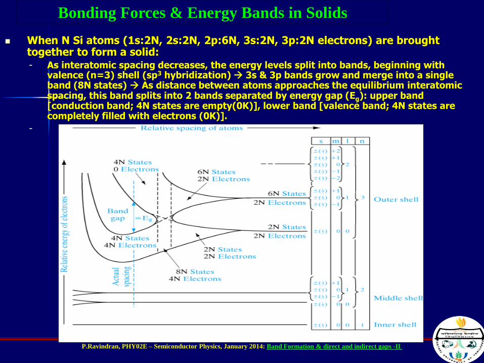
Bonding Forces & Energy Bands in SolidsEnergy Band
P.Ravindran, PHY02E – Semiconductor Physics, January 2014: Band Formation & direct and indirect gaps -II
When N Si atoms (1s:2N, 2s:2N, 2p:6N, 3s:2N, 3p:2N electrons) are brought together to form a solid:- As interatomic spacing decreases, the energy levels split into bands, beginning with
valence (n=3) shell (sp3 hybridization) 3s & 3p bands grow and merge into a single band (8N states) As distance between atoms approaches the equilibrium interatomicspacing, this band splits into 2 bands separated by energy gap (Eg): upper band [conduction band; 4N states are empty(0K)], lower band [valence band; 4N states are completely filled with electrons (0K)].
-
Bonding Forces & Energy Bands in Solids

P.Ravindran, PHY02E – Semiconductor Physics, January 2014: Band Formation & direct and indirect gaps -II
Review of Energy Bands (2)
The permitted energies that an
electron can occupy in the
isolated atoms are split into
energy bands as the atoms get
closer to each other.
This can also be visualized in
terms of an overlap of the
electron wave functions.
Holden A., The nature of solids,
Dover Publications, 1965
Outer
shell
Since the solid is made of a very large number
of atoms (N), these bands are actually
constituted by N levels of energies (almost a
continuum!). The position of upper and lower
extreme of each band is however independent of
N (depends only on the materials).

P.Ravindran, PHY02E – Semiconductor Physics, January 2014: Band Formation & direct and indirect gaps -II
Review of Energy Bands (3)
rrr EUm
2
2
2
Mathematically, it means solving the time-independent
Schrödinger’s equation:
where U(r) is the periodic effective potential energy that
describes the arrangement of atoms in the crystal.
e.g. a 1-D crystal could for instance
be represented in the following
manner:
a + b
a + b
a
b
U
o
x = 0
Adapted from: R. Eisberg, R.
Resnick, Quantum physics of
atoms, molecules, solids, nuclei,
and particles (2nd ed.), Wiley,
1985

P.Ravindran, PHY02E – Semiconductor Physics, January 2014: Band Formation & direct and indirect gaps -II
Review of Energy Bands (4)
Usually given form of a “band diagram” E vs k.
Yu, P.Y.,
Cardona, M.,
Fundamentals
of
semiconductors
, Springer,
2005
e.g. GaAs crystal
Cohen M.L., Chelikowski, J.R.,
Electronic Structure and Optical
Properties of semiconductors, Springer,
1989
Eg ~ 1.4
eV
Actual band diagram
For device description a much more simple
and practical representation is typically
used:
Eg
Ec
Ev

P.Ravindran, PHY02E – Semiconductor Physics, January 2014: Band Formation & direct and indirect gaps -II
Review of Energy Bands (5)
Direct band gap semiconductors (e.g. GaAs, InP, InAs, GaSb)
Cohen M.L., Chelikowski, J.R.,
Electronic Structure and Optical
Properties of semiconductors,
Springer, 1989
Eg ~
1.4 eV
The minimum of the
conduction band occurs
at the same k value as
the valence band
maximum.

P.Ravindran, PHY02E – Semiconductor Physics, January 2014: Band Formation & direct and indirect gaps -II
Review of Energy Bands (6)
Indirect band gap semiconductors (e.g. Si, Ge, AlAs, GaP, AlSb)
Cohen M.L., Chelikowski, J.R., Electronic Structure and Optical
Properties of semiconductors, Springer, 1989
Eg ~ 2.3 eV
The minimum of the
conduction band does not
occur at the same k value
as the valence band
maximum.
An electron promoted to
the conduction band
requires a change of its
momentum to make the
transition to the valence
band (typ. occurs via
lattice vibrations).

P.Ravindran, PHY02E – Semiconductor Physics, January 2014: Band Formation & direct and indirect gaps -II
E (energy) - k (propagation constant; wave vector) relationship:
- Free electron satisfies “k=<p>/ħ”
- For e- within a periodic lattice( has a periodic potential function) : energy gap Eg appears in E-k characteristics
4) Direct/Indirect Semiconductors
• Direct Semiconductors:
- It has a min. in CB & a max. in VB for the same k value (k=0).
- An electron in the CB min. can fall to an empty state in the VB max.,
giving off energy difference Eg as a photon of light without a change
in k (or p) value. used for semiconductor LED, laser
- ex) GaAs, AlxGa1-xAs(x<0.38), GaAs1-xPx(x<0.45)
electron) free(222
1 222
2
m
k
m
pmvE
• Indirect Semiconductors:
- It has its VB max. at a different k value than its CB min.
- When an electron in the CB min. falls to an empty state in the
VB max., 1) it falls first to defect state (Et) within the band
gap, giving off energy difference as heat with a change in k (or
p) value. 2) it falls then to the VB max., giving off energy
difference Et as a photon of light without a change in k (or p)
value.
- ex) Si, AlxGa1-xAs(1x>0.38), GaAs1-xPx(1x>0.45)
Bonding Forces & Energy Bands in
Solids

P.Ravindran, PHY02E – Semiconductor Physics, January 2014: Band Formation & direct and indirect gaps -II
Two semiconductors types :direct and indirect gap;
On direct gap semiconductor,such as GaAs, an electron at theminimal CB (Conduction Band)can deexcite to an unoccupied statein the VB (Valence Band) throughthe emission of a photon withenergy equaling Eg.
Direct & Indirect band gaps
Indirect transition via phonon.

P.Ravindran, PHY02E – Semiconductor Physics, January 2014: Band Formation & direct and indirect gaps -II
• Let us consider recombination of an electron and a hole,
accompanied by the emission of a photon.
• The simplified and most probable recombination process will
be that where the electron and hole have the same momentum
value. This is a direct-band-gap material.
• For indirect-band-gap materials, the conduction –band
minimum and the valence band maximum energy levels occur
at different values of momentum.
• Here band-to-band recombination must involve a third
particle to conserve momentum, since the photon momentum
is very small. Phonons (i.e. Crystal lattice vibrations) serve
this purpose.
Recombination in direct and indirect bandgap materials
P.Ravindran, PHY02E – Semiconductor Physics, January 2014: Band Formation & direct and indirect gaps -II
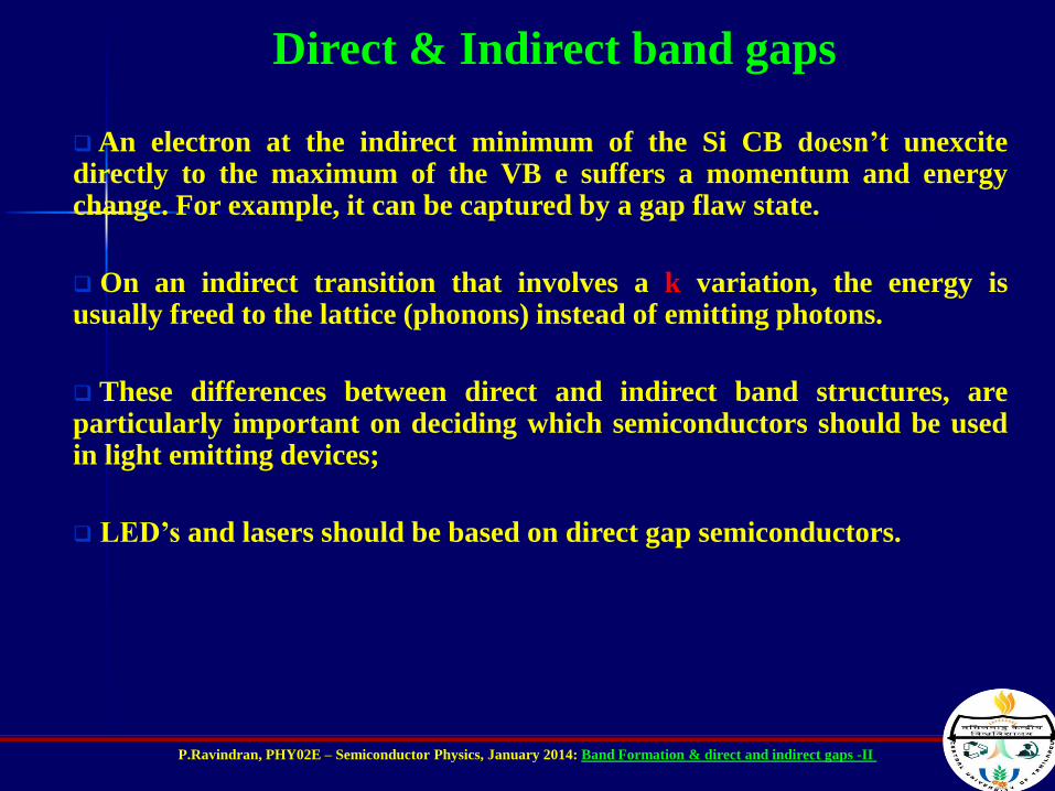
An electron at the indirect minimum of the Si CB doesn’t unexcitedirectly to the maximum of the VB e suffers a momentum and energychange. For example, it can be captured by a gap flaw state.
On an indirect transition that involves a k variation, the energy isusually freed to the lattice (phonons) instead of emitting photons.
These differences between direct and indirect band structures, areparticularly important on deciding which semiconductors should be usedin light emitting devices;
LED’s and lasers should be based on direct gap semiconductors.
Direct & Indirect band gaps

P.Ravindran, PHY02E – Semiconductor Physics, January 2014: Band Formation & direct and indirect gaps -II
Energy Band
A simplified energy band diagram with the highest almost-filled band
and the lowest almost-empty band.
valence band edge
conduction band edge
vacuum level
: electron affinity
P.Ravindran, PHY02E – Semiconductor Physics, January 2014: Band Formation & direct and indirect gaps -II
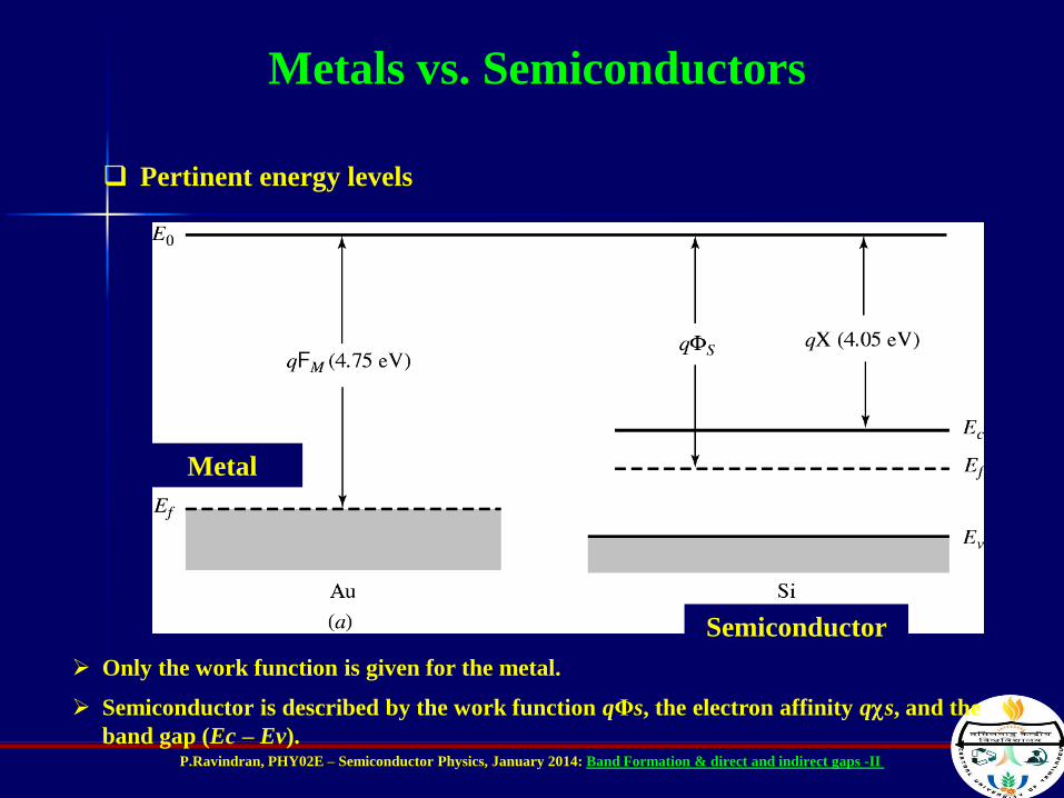
Only the work function is given for the metal.
Semiconductor is described by the work function qΦs, the electron affinity qs, and the
band gap (Ec – Ev).
Metals vs. Semiconductors
Pertinent energy levels
Metal
Semiconductor

P.Ravindran, PHY02E – Semiconductor Physics, January 2014: Band Formation & direct and indirect gaps -II 20
The Fermi-level in semiconductors
Formal definition of the Fermi-level: the energy level where the
probability of occupancy is 0.5:
In case of intrinsic semiconductor this is in the middle of the band gap.
This is the intrinsic Fermi-level Wi
5.0
exp1
1)(
kT
WWWf
F
2
vcF
WWW
electrons
holes

P.Ravindran, PHY02E – Semiconductor Physics, January 2014: Band Formation & direct and indirect gaps -II
Fermi Level in metals
• In metals the Femi level is defined as the top most occupied energy level. Also
defined as the energy level from where one can remove an electron to vaccum
with minimum Energy.
Focus on the electrons near the filled/empty boundary (i.e. top most occupied
band. Each material’s energy state distribution is unique; different EF.
E=0 (vacuum level)
EF (Fermi level)
Minimum
energy to
remove
electron
from
sample
Metal 1Metal 2
EF (Fermi level)
The closer an electron is to the vacuum level, the weaker it is bound to
the solid or the more energetic is the electron.

P.Ravindran, PHY02E – Semiconductor Physics, January 2014: Band Formation & direct and indirect gaps -II
ENERGY GAP

P.Ravindran, PHY02E – Semiconductor Physics, January 2014: Band Formation & direct and indirect gaps -II
For GaAs, calculate a typical (band gap) photon energy and momentum , and compare this with a typical phonon energy and momentum that might be expected with this material.
.:: CALCULATION
photonphonon
E(photon) = Eg(GaAs) = 1.43 ev
E(photon) = h = hc / λ
c= 3x10⁸ m/sec
P = h / λ h=6.63x10⁻³⁴ J-sec
λ (photon)= 1.24 / 1.43 = 0.88 μm
P(photon) = h / λ = 7.53 x 10⁻²⁸ kg-m/sec
E(phonon) = h = hvs / λ
= hvs / a0
λ (phonon) ~a0 = lattice constant =5.65x10⁻¹⁰ m
Vs= 5x10³ m/sec ( velocity of sound)
E(phonon) = hvs / a0 =0.037 eV
P(phonon)= h / λ = h / a0 = 1.17x10⁻²⁴ kg-m/sec

P.Ravindran, PHY02E – Semiconductor Physics, January 2014: Band Formation & direct and indirect gaps -II
Photon energy = 1.43 eV
Phonon energy = 37 meV
Photon momentum = 7.53 x 10⁻²⁸ kg-m/sec
Phonon momentum = 1.17 x 10⁻²⁴ kg-m/sec
Photons carry large energies but negligible amount of momentum.
On the other hand, phonons carry very little energy but significant
amount of momentum.

P.Ravindran, PHY02E – Semiconductor Physics, January 2014: Band Formation & direct and indirect gaps -II
Absorption Coefficient
][
24.1][
eVEm
g
g
Absorbed Photon create Electron-Hole Pair.
Cut-off wavelength vs. Energy
bandgap
xeIxI
0)( Absorption coefficient
Incident photons become absorbed as they travel in the
semiconductor and light intensity decays exponentially
with distance into the semiconductor.

P.Ravindran, PHY02E – Semiconductor Physics, January 2014: Band Formation & direct and indirect gaps -II
Absorption Coefficient
Absorption
coefficient α is a
material property.
Most of the photon
absorption (63%)
occurs over a
distance 1/α (it is
called penetration
depth δ)

P.Ravindran, PHY02E – Semiconductor Physics, January 2014: Band Formation & direct and indirect gaps -II
Absorption Coefficient
0.2 0.4 0.6 0.8 1.2 1.4 1.6 1.8
Wavelength (mm)
Ge
Si
In0.7Ga0.3As0.64P0.36
InP
GaAs
a-Si:H
123450.9 0.8 0.7
1 103
1 104
1 105
1 106
1 107
1 108
Photon energy (eV)
Ab
sorp
tion
Coeff
icie
nt
(m-1
)
1.0
In0.53Ga0.47As
Absorption The indirect-gap materials are shown
with a broken line.

P.Ravindran, PHY02E – Semiconductor Physics, January 2014: Band Formation & direct and indirect gaps -II
Band edge absorption in indirect gap semiconductor
The indirect transition involve both photons
and phonons (h, hq ):
.
,
qkk
EE
if
if
This is a second-order process, the transition
rate is much smaller than for direct absorption.
Comparison of the absorption coefficient of GaAs
and Silicon near their band edges. GaAs has a
direct band gap at 1.42 eV, while silicon has an
indirect gap at 1.12 eV. The absorption rises much
faster with frequency in a direct gap material, and
exceeds the indirect material.
Absorption coefficient of indirect band gap:
.)()(,
.)()(,
2
1
2
g
d
g
i
EdirectFor
EindirectFor
The differences:
1. Threshold;
2. Frequency dependence.
The differences provide a way to determine
whether the band gap is direct or not.
As T decrease, phonons decrease
gradually. At very low T, no phonons excited
with enough energy. Thus at the lowest T, the
indirect absorption edge is determined by
phonon emission rather than phonon absorption;
5. The direct absorption dominates over the
indirect processes once h > 0,8eV,
is the band gap for the transition at the eVEwhereE dir
g
dir
g 8.0),(2

P.Ravindran, PHY02E – Semiconductor Physics, January 2014: Band Formation & direct and indirect gaps -II
Band edge absorption in indirect gap semiconductor Band structure of germanium.
1. The lowest conduction band minimum
occurs at the L point (k=/a(1,1,1), not at
(k=0);
2. Indirect gap=0.66eV, direct gap ()= 0.8eV;
The absorption coefficient of germanium
1. vs h close to the band gap at 0.66 eV ;
2. The straight line extrapolates back to 0.65 eV,
which indicates that a phonon(TA)of energy ~
0.01 eV has been absorbed and q (phonon)
= k(electron) at L-point of the Brillouin zone;
3. A tail down to 0.6 eV, this is caused by absor-
ption of the higher frequency and also multi-
phonons absorption;
4. The temperature dependence of the absorption
edge:
Table 3.1
1)/exp(
1)(
TkEEf
B
BE
Bose-Einstein
Formula

P.Ravindran, PHY02E – Semiconductor Physics, January 2014: Band Formation & direct and indirect gaps -II
Th e interband absorption spectrum of siliconThe band structure of silicon
Eg is indirect and occurs at 1.1 eV;
E1 and E2 are the separation of the bands at the L and X points, where the conduction and valence are
approximately parallel along the (111) and (100).
E1 = 3.5 eV is the minimum direct separation, and corresponds to the sharp increase in absorption at E1, and
E2 correspond to the absorption maximum at 4.3 eV. Absorption at these energies is very high due to the Van
Hove singularities in the joint density of states ( band are parallel. E for direct transition does not depend on
k, dE/dk =0, g(E) diverges (critical point)
Interband absorption above the band edge
1. The optical properties at the band edge
determine the emission spectra;
.)()(,
.)()(,
2
1
2
g
d
g
i
EdirectFor
EindirectFor
2. The spectrum can be worked out by
dE/dk from the full band structure.
dkdE
kgEg
/
)(2)(

P.Ravindran, PHY02E – Semiconductor Physics, January 2014: Band Formation & direct and indirect gaps -II
Absorption Coefficient
E
CB
VB
k–k
Direct Bandgap Eg
E
k–k
VB
CBIndirect Bandgap
Photon
Phonons
Photon absorption in
an indirect bandgap semiconductor
EgEC
EV
EC
EV
Photon absorption in
a direct bandgap semiconductor.
Photon
P.Ravindran, PHY02E – Semiconductor Physics, January 2014: Band Formation & direct and indirect gaps -II
Absorption Coefficient
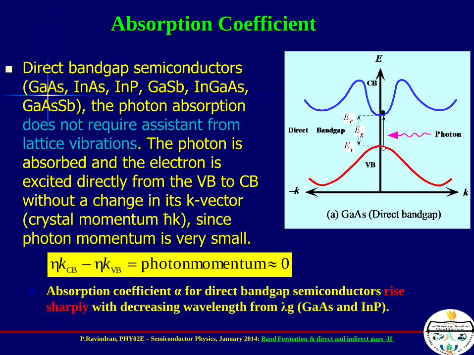
Direct bandgap semiconductors (GaAs, InAs, InP, GaSb, InGaAs, GaAsSb), the photon absorption does not require assistant from lattice vibrations. The photon is absorbed and the electron is excited directly from the VB to CB without a change in its k-vector (crystal momentum ħk), since photon momentum is very small.
0 momentumphoton VBCB
kk
Absorption coefficient α for direct bandgap semiconductors rise
sharply with decreasing wavelength from λg (GaAs and InP).

P.Ravindran, PHY02E – Semiconductor Physics, January 2014: Band Formation & direct and indirect gaps -II
Absorption Coefficient
Indirect bandgapsemiconductors (Si and Ge), the photon absorption requires assistant from lattice vibrations (phonon). If K is wave vector of lattice wave, then ħK represents the momentum associated with lattice vibration ħK is
a phonon momentum.Kkk momentumphonon
VBCB
Thus the probability of photon absorption is not as high as
in a direct transition and the λg is not as sharp as for direct
bandgap semiconductors.

P.Ravindran, PHY02E – Semiconductor Physics, January 2014: Band Formation & direct and indirect gaps -II 34
Absorption coefficient,
of a material determines generation as a function of wavelength
small for photons with energy below EG –no absorption below band gap.
For photon energies above Eg, will determine the critical thickness of absorption.

P.Ravindran, PHY02E – Semiconductor Physics, January 2014: Band Formation & direct and indirect gaps -II 35
Absorption coefficient
Absorption coefficient strongly affected by type of band gap.
Crystal momentum, p
Energy, E
EC
EV
hh1
2
Phonon emission
Phonon absorption
EG -- Ep
EG + EpEC
EV
Energy, E
Crystal momentum, p
Direct band gapIndirect band gap

P.Ravindran, PHY02E – Semiconductor Physics, January 2014: Band Formation & direct and indirect gaps -II
ZnO(direct band gap)
Optical band gap
- direct n = ½
- direct forbidden n = 3/2
- indirect n = 2
- indirect forbidden n = 3