ProfileofSubraSuresh - Ju Li
14
PROFILE Profile of Subra Suresh Sandeep Ravindran, Science Writer During his long and distinguished career, Subra Suresh has made crucial contributions to the field of engineering. While finishing up high school in India in the 1970s, however, Suresh was not even sure of going to college, let alone becoming an engineer. Nonetheless, Suresh decided to take a shot at the entrance examination for the prestigious Indian Insti- tutes of Technology. “A month before my exam, I bought a book to prepare and worked through some practice questions and just thought, go try it,” Suresh says. “To my surprise, I got in.” His degree in mechan- ical engineering from Indian Institutes of Technology Madras would turn out to be the starting point of a wide-ranging research career. Suresh’s research interests would eventually span engineering, basic science, and medicine. His multi- disciplinary work led to elected memberships in all three US National Academies: The National Academy of Engineering in 2002, the National Academy of Sci- ences in 2012, and the National Academy of Medicine in 2013. Suresh has held several prestigious positions, from being dean of Massachusetts Institute of Technology’s School of Engineering and president of Carnegie Mellon University to leading the National Science Foundation (NSF) of the United States. Now President of Nanyang Technological University, Singapore, Suresh continues to push forward in research with his recent work on deforming nanoscale diamond. In his Inaugural Article (1), Suresh and his colleagues show computationally that it is possible to make nanoscale diamond behave like a metal with respect to select properties, which would open up a wide array of ap- plications in microelectronics, optoelectronics, and solar energy. Spanning Many Disciplines After obtaining his bachelor’s degree at Indian Insti- tutes of Technology Madras, a scholarship offer led Suresh to attend Iowa State University for a Master’s degree in mechanical engineering. When he left for the Massachusetts Institute of Technology (MIT) two years later for a doctorate, Suresh joined the materials group in mechanical engineering, beginning his foray into materials science. After just a year and a half into his doctoral work at MIT, Suresh’s thesis committee deemed he was ready to receive a doctorate. “I was just stunned when they told me I was ready to defend my ScD [Doctor of Science] thesis,” he says. Suresh had finished so quickly that he was not yet sure about the next step. So, when his thesis advisor moved to the University of California, Berkeley, and offered him a postdoctoral fellowship, Suresh accepted. After two years at Berkeley, Brown University of- fered Suresh a faculty position. “They were looking for someone to bridge mechanical engineering and ma- terials science, and they thought I would be the right candidate for it,” says Suresh. “That’s how I migrated more and more into materials science,” he says. Brown granted Suresh tenure in less than three years, and during his 10 years there Suresh worked mainly on structural materials, such as steel, aluminum, and ce- ramics, work that culminated in his first book, Fatigue of Materials (2). Before long, MIT approached him, looking for a materials science professor with a background in mechanical engineering. “They made me an offer I couldn’t say no to, and so I went back to MIT as the R. P. Simmons Professor in 1993,” says Suresh. With a Subra Suresh. Image credit: Nanyang Technological University, Singapore. Published under the PNAS license. This is a Profile of a member of the National Academy of Sciences to accompany the member’s Inaugural Article, 10.1073/pnas.2013565117. First published October 5, 2020. 25192–25194 | PNAS | October 13, 2020 | vol. 117 | no. 41 www.pnas.org/cgi/doi/10.1073/pnas.2018742117 PROFILE Downloaded at MIT LIBRARIES on October 30, 2020
Transcript of ProfileofSubraSuresh - Ju Li

PROFILE
Profile of Subra SureshSandeep Ravindran, Science Writer
During his long and distinguished career, SubraSuresh has made crucial contributions to the field ofengineering. While finishing up high school in India inthe 1970s, however, Suresh was not even sure ofgoing to college, let alone becoming an engineer.Nonetheless, Suresh decided to take a shot at theentrance examination for the prestigious Indian Insti-tutes of Technology. “A month before my exam, Ibought a book to prepare and worked through somepractice questions and just thought, go try it,” Sureshsays. “To my surprise, I got in.” His degree in mechan-ical engineering from Indian Institutes of TechnologyMadras would turn out to be the starting point of awide-ranging research career.
Suresh’s research interests would eventually spanengineering, basic science, and medicine. His multi-disciplinary work led to elected memberships in allthree US National Academies: The National Academyof Engineering in 2002, the National Academy of Sci-ences in 2012, and the National Academy of Medicinein 2013.
Suresh has held several prestigious positions, frombeing dean of Massachusetts Institute of Technology’sSchool of Engineering and president of CarnegieMellon University to leading the National Science
Foundation (NSF) of the United States. Now Presidentof Nanyang Technological University, Singapore,Suresh continues to push forward in research with hisrecent work on deforming nanoscale diamond. In hisInaugural Article (1), Suresh and his colleagues showcomputationally that it is possible to make nanoscalediamond behave like a metal with respect to selectproperties, which would open up a wide array of ap-plications in microelectronics, optoelectronics, andsolar energy.
Spanning Many DisciplinesAfter obtaining his bachelor’s degree at Indian Insti-tutes of Technology Madras, a scholarship offer ledSuresh to attend Iowa State University for a Master’sdegree in mechanical engineering. When he left forthe Massachusetts Institute of Technology (MIT) twoyears later for a doctorate, Suresh joined the materialsgroup in mechanical engineering, beginning his forayinto materials science.
After just a year and a half into his doctoral work atMIT, Suresh’s thesis committee deemed he was readyto receive a doctorate. “I was just stunned when theytold me I was ready to defend my ScD [Doctor ofScience] thesis,” he says. Suresh had finished soquickly that he was not yet sure about the next step.So, when his thesis advisor moved to the University ofCalifornia, Berkeley, and offered him a postdoctoralfellowship, Suresh accepted.
After two years at Berkeley, Brown University of-fered Suresh a faculty position. “They were looking forsomeone to bridge mechanical engineering and ma-terials science, and they thought I would be the rightcandidate for it,” says Suresh. “That’s how I migratedmore and more into materials science,” he says.Brown granted Suresh tenure in less than three years,and during his 10 years there Suresh workedmainly onstructural materials, such as steel, aluminum, and ce-ramics, work that culminated in his first book, Fatigueof Materials (2).
Before long, MIT approached him, looking for amaterials science professor with a background inmechanical engineering. “They made me an offer Icouldn’t say no to, and so I went back to MIT as theR. P. Simmons Professor in 1993,” says Suresh. With aSubra Suresh. Image credit: Nanyang Technological University, Singapore.
Published under the PNAS license.This is a Profile of a member of the National Academy of Sciences to accompany the member’s Inaugural Article, 10.1073/pnas.2013565117.First published October 5, 2020.
25192–25194 | PNAS | October 13, 2020 | vol. 117 | no. 41 www.pnas.org/cgi/doi/10.1073/pnas.2018742117
PRO
FIL
E
Dow
nloa
ded
at M
IT L
IBR
AR
IES
on
Oct
ober
30,
202
0

joint appointment in materials science andmechanicalengineering, Suresh changed his research focus fromlarge structures to small ones. He worked mainly onmicroelectronics and film coatings, work that led to asecond book, Thin Film Materials (3).
In 2003, Suresh pivoted again, this time to bio-medical sciences and engineering. “We started look-ing at red blood cells and the connection betweenmechanical properties at the cellular and molecularlevel, and human diseases, such as malaria and sicklecell anemia,” he says. Over the next several years,Suresh and his research group published prolifically atthe intersection of engineering and physiology (4–7).
In 2010, Suresh was offered a challenge on a dif-ferent scale. “President Obama nominated me to bethe director of the National Science Foundation,” saysSuresh. “That was a great honor when the WhiteHouse called.”
Driving Innovation at the NSFAs director of the NSF, Suresh launched the Innova-tion Corps (I-Corps), an initiative aimed at helpingresearchers across the country commercialize theirdiscoveries from basic research. “I felt that there was alot of very good science that’s funded by NSF withtaxpayer funds that could potentially lead to compa-nies or economic value or patents, but that never seesthe light of day,” he says. “I believe that any smart,young person anywhere can come up with a brilliantidea,” says Suresh. “But if you happen to be in a placewhere there’s no infrastructure for commercialization,no matter how good an idea you have, it doesn’t havea chance to come to fruition,” he says.
Through the I-Corps, researchers could submit ashort proposal to take their existing research beyondpublications. “If your proposal is accepted you’ll re-ceive a small grant, on the order of $50,000, for a shortperiod of time—six months to one year—to explore ifyour idea has any chance of going further,” saysSuresh. After a year of funding, researchers couldevaluate whether their idea had any chance of suc-ceeding, in which case they could found a company orlook for outside funding to take the idea further. “NSFis just a facilitator, to enable the connections and thenetworking,” says Suresh.
Suresh launched I-Corps in 2011 with $6 million ofthe NSF’s then $7 billion budget, but the initiative hassince come a long way. “To my pleasant surprise, ithas become one of the most successful programsnow,” says Suresh. I-Corps now has an annual budgetof $30 million and has funded more than 1,200 pro-jects between 2012 and 2018 across 247 UnitedStates universities, which directly led to 577 compa-nies. The program has spawned numerous imitators,not just at other United States agencies, such as theDepartment of Energy and the National Institutes ofHealth, but across the world, including in Ireland,Australia, and Singapore. “They all have I-Corps–likeprograms now,” says Suresh. “So this is one of themost satisfying things I did at the NSF,” he says.
After his stint at the NSF, Suresh became presidentof Carnegie Mellon University in 2013 and launched
several initiatives over the next four years. Theseprograms included the Global Learning Council toaccelerate the impact of technology-enhanced learn-ing, an ambitious infrastructure development effort, aCenter for Entrepreneurship, and the PresidentialFellowships and Scholarships Program to support topstudents. During his tenure as president, CarnegieMellon University’s undergraduate freshman class inthe School of Computer Science comprised a record48% of women students, three times the United Statesnational average.
Improving the Performance of DiamondsIn 2017, Suresh was appointed president of NanyangTechnological University, Singapore. While helming amajor research university, he also began research onnanoscale diamonds.
“We had a hypothesis that materials often behavesurprisingly differently at the nanoscale than at themacro- or even micro-scale,” says Suresh. In additionto being the hardest material, diamond is extremelybrittle. “If you try to break it, nothing will happen atfirst until you impose a very high load, and then all of asudden it will crack and break catastrophically,” saysSuresh. “When we go to the nanoscale, things be-come stronger, there is more surface area per unitvolume, and the density of defects becomes smaller.So we thought nanodiamondmight behave differentlythan bulk diamond that you can buy in a store,”says Suresh.
In a 2018 study, Suresh and his colleagues grewsynthetic diamond needles tens of nanometers in di-ameter and a few hundred nanometers in length on asilicon surface (8). Whereas bulk diamond would typ-ically fracture if pushed beyond a strain of ∼0.15%, thenanoneedles of diamond could be experimentallybent all of the way up to a local maximum strain ofmore than 9% and still return to their original shape.“To our surprise, we could actually bend the needlelike you would bend a paperclip,” says Suresh. “Wehad to videotape the experiment to convince ou-rselves and others that you can actually bend dia-mond,” he says. Independent validation followedwithin a year when a group in China reproduced theresults using natural diamond (9).
Bending diamond is not just a matter of intellectualcuriosity. Diamond has appealing properties not onlyas the hardest material found in nature, but also as asemiconductor. Previous research had shown thatstraining silicon could improve its semiconductorproperties by changing its band gap. “If we can benda nanoscale diamond by 9%, maybe you can changethe band gap by straining on demand withoutchanging chemistry,” says Suresh. Modulating theband gap of diamond solely through mechanicalmeans could lead to numerous practical applicationsin solar cells, optoelectronics, and microelectronics.
In a 2019 article (10), Suresh and his collaboratorsshowed computationally that straining diamond couldpotentially change its band gap from 5.6 eV to ∼2 to 3eV, bringing it within the range of currently used
Ravindran PNAS | October 13, 2020 | vol. 117 | no. 41 | 25193
Dow
nloa
ded
at M
IT L
IBR
AR
IES
on
Oct
ober
30,
202
0
semiconductor materials, such as silicon carbide andgallium nitride. But Suresh was not content to stop there.
In his Inaugural Article (1), Suresh exploredwhether straining diamond could reduce its band gapdown to zero, essentially making it behave like ametal. He also wondered if he could achieve this featunder strains that had already been shown experi-mentally and without triggering a phase change thatwould convert diamond into graphite. “We showedusing machine learning that the answer to all of thosequestions is yes,” says Suresh. “Using amounts ofstrain that are already known to be possible experi-mentally, you can make the band gap of diamondvanish,” he says. The same method could be used toimprove the properties and performance of mostsemiconductor materials with information, communi-cation, and energy applications, says Suresh.
This work continues Suresh’s long tradition ofmultidisciplinary science. “This is materials science
meets computer science meets mathematics and dataanalytics and artificial intelligence,” he says. “Inter-disciplinary research has come a long way from when Ifirst went to Brown in the 1980s, where even me-chanical engineers working with materials scientistswas a very big deal,” says Suresh.
For all his success across varied disciplines, Sureshcherishes his mechanical engineering roots, and oneof his latest honors harkens back to those roots. Sureshis the recipient of the 2020 American Society of Me-chanical Engineers (ASME) medal, the highest honorgiven annually to a single individual chosen from thesociety’s global membership of more than 100,000.He says the award brings back nostalgic memories ofjoining ASME as a student member, when he firstcame to Iowa State University in the late 1970s at thestart of his illustrious career. “It’s very special to re-ceive that from a society that I’ve been part of far morethan 40 years,” he says.
1 Z. Shi et al., Metallization of diamond. Proc. Natl. Acad. Sci. U.S.A. 117, 24634–24639 (2020).2 S. Suresh, Fatigue of Materials, (Cambridge University Press, 2nd Ed., 1998).3 L. B. Freund, S. Suresh, Thin Film Materials: Stress, Defect Formation and Surface Evolution, (Cambridge University Press, 2004).4 G. Bao, S. Suresh, Cell and molecular mechanics of biological materials. Nat. Mater. 2, 715–725 (2003).5 Y. Park et al., Refractive index maps and membrane dynamics of human red blood cells parasitized by Plasmodium falciparum. Proc.Natl. Acad. Sci. U.S.A. 105, 13730–13735 (2008).
6 E. Du, M. Diez-Silva, G. J. Kato, M. Dao, S. Suresh, Kinetics of sickle cell biorheology and implications for painful vasoocclusive crisis.Proc. Natl. Acad. Sci. U.S.A. 112, 1422–1427 (2015).
7 I. V. Pivkin et al., Biomechanics of red blood cells in human spleen and consequences for physiology and disease. Proc. Natl. Acad.Sci. U.S.A. 113, 7804–7809 (2016).
8 A. Banerjee et al., Ultralarge elastic deformation of nanoscale diamond. Science 360, 300–302 (2018).9 A. Nie et al., Approaching diamond’s theoretical elasticity and strength limits. Nat. Commun. 10, 5533 (2019).
10 Z. Shi et al., Deep elastic strain engineering of bandgap through machine learning. Proc. Natl. Acad. Sci. U.S.A. 116,4117–4122 (2019).
25194 | www.pnas.org/cgi/doi/10.1073/pnas.2018742117 Ravindran
Dow
nloa
ded
at M
IT L
IBR
AR
IES
on
Oct
ober
30,
202
0
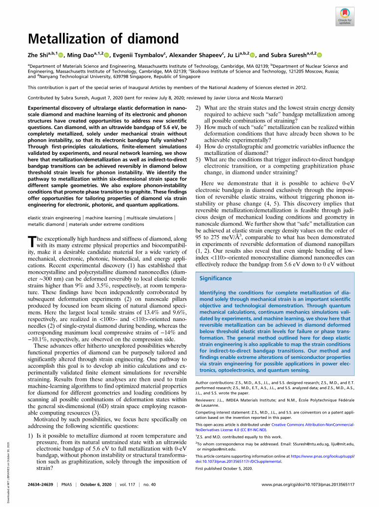
Metallization of diamondZhe Shia,b,1, Ming Daoa,1,2
, Evgenii Tsymbalovc, Alexander Shapeevc, Ju Lia,b,2, and Subra Suresha,d,2
aDepartment of Materials Science and Engineering, Massachusetts Institute of Technology, Cambridge, MA 02139; bDepartment of Nuclear Science andEngineering, Massachusetts Institute of Technology, Cambridge, MA 02139; cSkolkovo Institute of Science and Technology, 121205 Moscow, Russia;and dNanyang Technological University, 639798 Singapore, Republic of Singapore
This contribution is part of the special series of Inaugural Articles by members of the National Academy of Sciences elected in 2012.
Contributed by Subra Suresh, August 7, 2020 (sent for review July 8, 2020; reviewed by Javier Llorca and Nicola Marzari)
Experimental discovery of ultralarge elastic deformation in nano-scale diamond and machine learning of its electronic and phononstructures have created opportunities to address new scientificquestions. Can diamond, with an ultrawide bandgap of 5.6 eV, becompletely metallized, solely under mechanical strain withoutphonon instability, so that its electronic bandgap fully vanishes?Through first-principles calculations, finite-element simulationsvalidated by experiments, and neural network learning, we showhere that metallization/demetallization as well as indirect-to-directbandgap transitions can be achieved reversibly in diamond belowthreshold strain levels for phonon instability. We identify thepathway to metallization within six-dimensional strain space fordifferent sample geometries. We also explore phonon-instabilityconditions that promote phase transition to graphite. These findingsoffer opportunities for tailoring properties of diamond via strainengineering for electronic, photonic, and quantum applications.
elastic strain engineering | machine learning | multiscale simulations |metallic diamond | materials under extreme conditions
The exceptionally high hardness and stiffness of diamond, alongwith its many extreme physical properties and biocompatibil-
ity, make it a desirable candidate material for a wide variety ofmechanical, electronic, photonic, biomedical, and energy appli-cations. Recent experimental discovery (1) has established thatmonocrystalline and polycrystalline diamond nanoneedles (diam-eter ∼300 nm) can be deformed reversibly to local elastic tensilestrains higher than 9% and 3.5%, respectively, at room tempera-ture. These findings have been independently corroborated bysubsequent deformation experiments (2) on nanoscale pillarsproduced by focused ion beam slicing of natural diamond speci-mens. Here the largest local tensile strains of 13.4% and 9.6%,respectively, are realized in <100>- and <110>-oriented nano-needles (2) of single-crystal diamond during bending, whereas thecorresponding maximum local compressive strains of −14% and−10.1%, respectively, are observed on the compression side.These advances offer hitherto unexplored possibilities whereby
functional properties of diamond can be purposely tailored andsignificantly altered through strain engineering. One pathway toaccomplish this goal is to develop ab initio calculations and ex-perimentally validated finite element simulations for reversiblestraining. Results from these analyses are then used to trainmachine-learning algorithms to find optimized material propertiesfor diamond for different geometries and loading conditions byscanning all possible combinations of deformation states withinthe general six-dimensional (6D) strain space employing reason-able computing resources (3).Motivated by such possibilities, we focus here specifically on
addressing the following scientific questions:
1) Is it possible to metallize diamond at room temperature andpressure, from its natural unstrained state with an ultrawideelectronic bandgap of 5.6 eV to full metallization with 0-eVbandgap, without phonon instability or structural transforma-tion such as graphitization, solely through the imposition ofstrain?
2) What are the strain states and the lowest strain energy densityrequired to achieve such “safe” bandgap metallization amongall possible combinations of straining?
3) How much of such “safe” metallization can be realized withindeformation conditions that have already been shown to beachievable experimentally?
4) How do crystallographic and geometric variables influence themetallization of diamond?
5) What are the conditions that trigger indirect-to-direct bandgapelectronic transition, or a competing graphitization phasechange, in diamond under straining?
Here we demonstrate that it is possible to achieve 0-eVelectronic bandgap in diamond exclusively through the imposi-tion of reversible elastic strains, without triggering phonon in-stability or phase change (4, 5). This discovery implies thatreversible metallization/demetallization is feasible through judi-cious design of mechanical loading conditions and geometry innanoscale diamond. We further show that “safe”metallization canbe achieved at elastic strain energy density values on the order of95 to 275 meV/Å3, comparable to what has been demonstratedin experiments of reversible deformation of diamond nanopillars(1, 2). Our results also reveal that even simple bending of low-index <110>-oriented monocrystalline diamond nanoneedles caneffectively reduce the bandgap from 5.6 eV down to 0 eV without
Significance
Identifying the conditions for complete metallization of dia-mond solely through mechanical strain is an important scientificobjective and technological demonstration. Through quantummechanical calculations, continuum mechanics simulations vali-dated by experiments, and machine learning, we show here thatreversible metallization can be achieved in diamond deformedbelow threshold elastic strain levels for failure or phase trans-formation. The general method outlined here for deep elasticstrain engineering is also applicable to map the strain conditionsfor indirect-to-direct bandgap transitions. Our method andfindings enable extreme alterations of semiconductor propertiesvia strain engineering for possible applications in power elec-tronics, optoelectronics, and quantum sensing.
Author contributions: Z.S., M.D., A.S., J.L., and S.S. designed research; Z.S., M.D., and E.T.performed research; Z.S., M.D., E.T., A.S., J.L., and S.S. analyzed data; and Z.S., M.D., A.S.,J.L., and S.S. wrote the paper.
Reviewers: J.L., IMDEA Materials Institute; and N.M., École Polytechnique Fédéralede Lausanne.
Competing interest statement: Z.S., M.D., J.L., and S.S. are coinventors on a patent appli-cation based on the invention reported in this paper.
This open access article is distributed under Creative Commons Attribution-NonCommercial-NoDerivatives License 4.0 (CC BY-NC-ND).1Z.S. and M.D. contributed equally to this work.2To whom correspondence may be addressed. Email: [email protected], [email protected],or [email protected].
This article contains supporting information online at https://www.pnas.org/lookup/suppl/doi:10.1073/pnas.2013565117/-/DCSupplemental.
First published October 5, 2020.
24634–24639 | PNAS | October 6, 2020 | vol. 117 | no. 40 www.pnas.org/cgi/doi/10.1073/pnas.2013565117
Dow
nloa
ded
at M
IT L
IBR
AR
IES
on
Oct
ober
30,
202
0

phonon instability, at about 10.8% local compressive elastic strain.Further bending the nanoneedle can, however, induce phononinstabilities (5) that lead to irreversible sp3 → sp2 (diamond tographite) phase transition or fracture. Indeed, plasticity inducedby such sp3 → sp2 phase transition has recently been observed inthe large bending of a single-crystalline diamond pillar (6), sub-stantially agreeing with our calculations. Similar graphitizationtransition is also seen in nanoindentation experiments (7). Navi-gating the treacherous elastic strain space above 80 meV/Å3 orat >9% local compressive or tensile principal elastic strain to in-duce complete metallization in diamond without encounteringphonon instabilities is a “holy grail” demonstration for powerelectronics, optoelectronics, and quantum sensing systems.Whether mechanically strained or not, the absence of imagi-
nary phonon frequency for the wavevector in the entire Brillouinzone is the hallmark of a locally stable crystal lattice (5, 8, 9). If astrained perfect crystal lattice has a stable phonon band struc-ture, then at T = 0 K and in the absence of defects such as freesurfaces, interfaces and dislocations, this lattice is guaranteed toavoid spontaneous phase transition or defect nucleation. Con-sequently, phonon stability is the minimal requirement for latticestability and loading reversibility (5). If such a phonon-stablediamond can have zero electronic bandgap, Eg = 0 eV (re-duced from Eg = 5.6 eV at zero strain), then this extreme elec-tronic material (10) is expected to demonstrate unprecedentedfunctional flexibility, from ultrawide bandgap semiconductor tothe far-infrared and even metallic, in one material, without anychange in chemical composition and possibly under dynamicloading. The electronic band structures of diamond under ten-sorial strain can be predicted with high accuracy based on abinitio density functional theory (DFT) followed by many-bodyGW (G, Green’s function; W, screened Coulomb interaction)calculations (11). However, because GW calculations are com-putationally expensive, it is necessary to invoke a stress–strainconstitutive law for modeling large elastic deformation of dia-mond in any arbitrary sample geometry, along with fast proxymodels for the electronic and phonon band structures. In thiswork, we employ machine-learning algorithms of band structures(3) based on an artificial neural network (NN) approach, so as toperform coupled ab initio and finite element calculations withconstitutive laws based on NNs (see Methods for details). Thecoupling of this simulation to loading and/or device geometryoptimization (12) and computer-aided design (13) provides aunique and hitherto unknown pathway to engineer “safe” met-allization in diamond.
We first present some 6D strain states in Fig. 1 which makethe bandgap of diamond vanish without phonon instability orgraphitization. In the crystallographic [100][010][001] coordinateframe, our calculations show that one such complete and “safe”metallization occurs when the local 6D strain state is (0.0536,−0.0206, −0.056, 0.0785, 0.0493, 0.0567). Fig. 1A is a k-space plotof the GW electronic band structure for diamond deformed tothis particular 6D strain state, resulting in a direct metal (see SIAppendix, Fig. S1 for comparison of GW electronic band struc-ture with that for DFT). Contours of strain energy density areplotted in two-dimensional (2D) strain space in Fig. 1B wherethe star symbol in black, represents h = 98.7 meV/Å3. Note thatthe strains and strain energy density values in Fig. 1 are com-parable to the values achieved experimentally (1, 2) in reversibleultra-large elastic bending of diamond nanoneedles or pillars.Fig. 2 further illustrates our discovery of the region of “safe”
metallization of diamond without phonon instability and dem-onstrates reversible indirect-to-direct bandgap transitions underlarge elastic strains. Possible strain states in the three-dimensional(3D) space of normal strains «11, «22, and «33, spanning −20%(i.e., compressive strain of 0.2) to +10% (i.e., tensile strain of 0.1)within which “safe” metallization is induced (highlighted in browncolor) are shown in Fig. 2A. Regions of metallization are alsoplotted in Fig. 2B in the 2D strain space of «11versus «22, with theother four strain components held fixed (i.e., formed as a result of2D projection out of 3D strain region tessellated by cubes on tothe plane «33 = −0.056 in Fig. 2A). The triangle data points ofdifferent colors in Fig. 2B represent results of computationalsimulations of the effect of mechanical strain on bandgap andband structure. Two types of “safe”metallization, direct metal andindirect metal (where the band-edge transition is indirect, i.e.,from two different k-points), are identified. The 2D region of di-rect metal, shaded in brown, encompasses the strain state repre-sented by the star symbol, which was discussed in Fig. 1. This zoneis embedded within the strain space of direct bandgap (blue re-gion, Fig. 2B). The region of indirect metal, also shaded in brown,is surrounded by the white zone representing the strain space forindirect bandgap (comprising magenta-colored data points fromour simulation). In Fig. 2C, the GW band structure is plotted inthe k-space to illustrate such indirect-metal state at point c (Fig.2B) inside this zone of “safe” metallization. Examples of nonzerodirect and indirect bandgap cases indicated by the band structureplots are shown in Fig. 2 D and E, respectively. The area shaded ingray outside of the dashed lines is the region of large elastic strainsand unstable metallization where phonon instability leading to
Fig. 1. Metallization of diamond. (A) Electronic band structure k-space plot showing complete closure of bandgap leading to metallization of diamondwhich is subjected to deformation at a 6D strain state of (0.0536, −0.0206, −0.056, 0.0785, 0.0493, 0.0567) in the [100][010][001] coordinate frame. An entireregion of strains exists for the metallization of diamond and a 2D cross-section plot of normal strain components «11 and «22 is illustrated in B. The axes in Bare absolute strain component values of «11 and «22, with the other four strain components fixed at −0.056, 0.0785, 0.0493, and 0.0567. Color contours in-dicate regions of constant elastic strain energy density (h) for different deformation states. The black star symbol denotes the strain energy density value, h =98.7 meV/Å3, which corresponds to the band structure plot shown in A.
Shi et al. PNAS | October 6, 2020 | vol. 117 | no. 40 | 24635
PHYS
ICS
INAUGURA
LART
ICLE
Dow
nloa
ded
at M
IT L
IBR
AR
IES
on
Oct
ober
30,
202
0

defect nucleation and/or phase transition occurs (5). Fig. 2F re-veals pronounced reduction in phonon frequency and the occur-rence of soft mode associated with strain point f in Fig. 2B wherephonon instability and associated phase transition from diamondto graphite takes place. The location of the special strain regioncontaining metallization is not unique in a general 6D strain hy-perspace and such stratified regions may exist in a broad range ofsemiconductors. Our findings offer a systematic strategy in thesearch for strain-engineered semiconductor-to-metal transition,indirect-to-direct bandgap transition, as well as phase transition.Experiments show that diamond nanoneedles exhibit ultra-
large elastic bending before fracture (1). Such deformation,resulting in local compressive strains larger than −10% andtensile strains in excess of 9%, is reversible upon release of theload. Here we apply simulations to determine bandgap modu-lation in bent diamond nanoneedles at maximum local strainlevels that are known to be experimentally feasible (SI Appendix,Table S1). Fig. 3A schematically illustrates the method whereby adiamond indenter tip pushes on a diamond nanoneedle to inducelarge deformation (1). The finite element method (FEM) is usedto simulate the sideward bending moment of the diamond needleupon contact with the indenter tip and account for nonlinearelasticity, orientation of the cubic lattice with respect to theneedle axis, the bending direction, and possible friction betweenthe indenter tip and the needle.Fig. 3B shows FEM results of local compressive and tensile
strains of the deformed geometry of <110> diamond nanoneedle,with the maximum compressive and tensile strains of −10.8% and9.6%, respectively. The accuracy of FEM predictions is validatedby direct comparison with experimentally measured indentationload plotted against displacement (1). The corresponding predic-tions, from our simulations, of the distribution of bandgap are alsoplotted in Fig. 3B. The onset of “safe”metallization appears in theseverely strained compressive side of the nanoneedle at a localstrain of −10.8%, as shown in Fig. 3C. The propensity towardincreasingly more metal-like behavior with increasing strain isindependent of friction between the indenter and the nanoneedle(see SI Appendix, Fig. S3). The <110> nanoneedle can withstandup to 12.1% local tensile strain before incurring phonon instabilityon the tensile side, at a bandgap of 0.62 eV, as shown in Fig. 3D.The maximum attainable local tensile strain of 9.6% on the tensileside of <110> single-crystal natural diamond samples (2), ascompared to theoretical predictions of higher values (SI Appendix,Fig. S4 and Table S1), could be attributed to the presence ofdislocations and/or other surface-related defects (14–17). Thecompressive side is more tolerant to deformation. The maximumattainable compressive strain could be on the order of −20% alonga low-index orientation (18), suggesting that there is room for ad-ditional elastic deformation after achieving “safe” metallization incompression-dominated regions. Note that due to the zero-pointmotion effect (19) and the Varshni effect (20), for physical exper-iments performed at room temperature, the bandgap of diamond isexpected to be even smaller than estimated here by 0.4 to 0.6 eV(21, 22). This understanding leads to the inference that safe met-allization in diamond can occur at elastic strain levels somewhatsmaller than indicated by our analysis, making it even more easilyachievable than appears from the quantitative results plotted here(see Methods for details).Crystallographic orientation of the nanoneedle axis is another
variable determining the extent of large deformation and theresultant bandgap modulation. This orientation effect is illus-trated in SI Appendix, Fig. S5 A and B. Among the three types ofnanoneedles studied, the <110>- and <111>-oriented nano-needles require relatively smaller tensile strains to reduce bandgapthrough straining, whereas the <100> orientation is the hardestorientation to reduce bandgap below 2 eV or approach metalli-zation. This distinction can be attributed to the difference inflexibility to access all six components of the strain tensor expressed
in the [100][010][001] coordinate frame. Despite the possibility ofextremely large strain in a <100>-oriented nanoneedle, this ori-entation primarily facilitates normal strains (with the shear com-ponents «23, «13, and «12 being relatively much smaller) and theresultant maximum bandgap reduction is limited before phononinstability is reached, causing fracture or phase transformation (5).For deformation of the <110>- and <111>-oriented needles, onthe other hand, it is relatively easier to initiate both normal andshear strain components necessary for band structure engineering(3, 23–25) and the resultant bandgap modulation. In the <111>-oriented needles, these strain conditions further facilitate indirect-to-direct bandgap transitions in diamond. The spatial evolution ofthe “safe” direct bandgap regions in our nanoneedles can be foundin SI Appendix, Fig. S5C. Bending direction is another geometricalfactor, as shown in SI Appendix, Fig. S5D. For a low-index-orientedneedle, we find bending direction has little influence on the max-imum bandgap reduction in the bent needle.Beyond the configurations considered here, more complex 3D
loading geometries with holes and notches through topologyoptimization (26) and micro- and nanomachining of geometricfeatures (27, 28) can be designed without exposing the metallizedzone to near-surface regions (29), further increasing possibilitiesfor metallizing diamond. These methods for deep elastic strainengineering are equally applicable to map the indirect-to-directbandgap transition locations in diamond for the most general 6Dstraining case, as indicated in Fig. 2 A, B, and D. When straineddiamond is transformed into a direct bandgap semiconductor,even only locally at the site of maximum strain, it would exhibit afundamental enhancement in its optical transitions around theadsorption edge compared to an undeformed diamond in itsnatural state. This transition arises from the absence of phononinvolvement (momentum change of electron) in the adsorption oremission process. Since absorbance increases exponentially withthickness in a material, a light energy conversion device based ondirect bandgap semiconductor with a high adsorption coefficientand rationally engineered bandgap value would require much lessthickness to absorb the same amount of light with a variety ofwavelengths, from the visible to the far-infrared. These consider-ations could pave the way for designing high-efficiency photodetectors and emitters from ultraviolet to the far-infrared on asingle piece of diamond. As photons and excitons are the primarytools for quantum information processing, this extreme ability tomold diamond’s band structure will also be highly consequentialfor quantum sensing and quantum computing applications.To perform simultaneous mechanical deformation and electronic
properties evaluation, further studies could combine in situ nano-electromechanical loading experiments inside a transmission elec-tron microscope with built-in electron energy loss spectroscopy(EELS). It is known (30–32) that EELS is reliable for assessing thebandgap value (including surface plasmon mapping) as well asindirect-to-direct bandgap transition in diamond. Indentation andanviling (compression under extreme pressures) coupled with in situphotoluminescence (33–35) or cathodoluminescence (36) spectros-copy as well as electrical resistivity measurement (37) further add tothe toolbox for characterization of mechanically induced propertiesincluding superconductivity of diamond (38–40).
MethodsFirst-Principles Calculations. The Vienna Ab initio Simulation Package (VASP)(41) was used for DFT calculations to predict the evolution of bandgap andband structure of diamond subjected to mechanical deformation. We in-voked the generalized gradient approximation in the form of Perdew–
Burke–Ernzerhof’s (PBE) exchange-correlation (42) functional and the pro-jector augmented wave method (43) in our DFT computation. A plane-wavebasis set with an energy cutoff of 600 eV was adopted to expand the elec-tronic wavefunctions. The Brillouin zone integration was conducted on a13 × 13 × 13 Monkhorst–Pack (44) k-point mesh. Atomic coordinates in all ofthe structures were relaxed until the maximum residual force was below0.0005 meV/Å.
24636 | www.pnas.org/cgi/doi/10.1073/pnas.2013565117 Shi et al.
Dow
nloa
ded
at M
IT L
IBR
AR
IES
on
Oct
ober
30,
202
0

Many-body GW corrections were performed when bandgap evaluationswere needed. It is known that an extremely accurate GW calculation wouldinvolve choosing “infinitely” large values for several interdependent pa-rameters (45, 46). Given the situation that we need to construct a hugedataset of GW bandgaps for machine-learning purposes and conduct manycalculations for varied 6D strain cases, we hereby struck a balance betweenefficiency and effectiveness. Specifically, we chose the q-grid to be 6 × 6 × 6,the screened cutoff to be 600 eV, and the number of bands for both di-electric matrix calculation and Coulomb hole summation to be 600. In ad-dition, beyond the single-shot G0W0 method, we allowed two to threeiterations of the Green’s function in our calculations to obtain accuratequasi-particle shifts. This partially self-consistent GW0 calculation is known toyield results that are in agreement with available experimental measure-ment for semiconductor materials (47) and better than plain DFT calculationsusing hybrid functionals (48). For undeformed diamond, our calculation indi-cates a +1.5-eV GW correction to the DFT–PBE bandgap, which matches valuesreported in recent literature (49). For general 6D strain cases, this correctionmay vary (see SI Appendix, Fig. S1 for an example). Diamond primitive cells
were used for DFT and GW calculations. All band structures were plotted byVASP with a Wannier90 interface (50–52).
We also acknowledge that, even at 0 K, due to the quantum zero-pointmotion, further corrections need to be made to the electronic levels of di-amond. This renormalization of bandgap could be −0.6 eV to −0.4 eV forundeformed diamond (21, 22). We consider this correction value to benegative in other cases of our interest. According to the temperature-dependent “adiabatic Allen–Heine formula” (19, 53), by setting T = 0 tozero-out the Bose–Einstein occupancy factors, the zero-point renormaliza-
tion of the band structure (ΔEZPnk) arising from the electron-phonon inter-
action could be expressed as
ΔEZPnk ≡ ΔEnk(T = 0) = ∑
ν
∫dqΩBZ
[∑n’
gnn’ν(k,q)
2«nk − «n’k+q
] + ΣDWnk ,
where «nk is the single-particle eigenvalue of an electron with crystal mo-mentum k in the band n, the integral is over the Brillouin zone of volume
Fig. 2. Stratification of the strain hyperspace into regions of metallization and bandgap transition in diamond. (A) Metallization in elastically strained di-amond for different values of normal strain components «11, «22, and «33, with the other three strain components held fixed. The plane with «33 = −0.056(colored as light green) cuts the 3D volume and results in a projection onto the «11–«22 2D plane. (B) Detailed characterization of the «11–«22 strain spaceincludes a region of direct metal (brown) strains within the region of direct bandgap (blue) strains and a region of indirect metal (brown) strains within thenonzero indirect bandgap strains (white zone with magenta symbols). The black star in indicates the same strain case (0.0536, −0.0206, −0.056, 0.0785, 0.0493,0.0567) discussed in Fig. 1. An alternative visualization of the metallization strains in A is presented in SI Appendix, Fig. S2. (C) GW band structure of thediamond strained within the “safe”metallization region resulting in an indirect metal. Strained diamond (D) with a direct bandgap (point d in B) and (E) withan indirect bandgap (point e in B). The strain region of phase transformation in diamond (usually associated with phonon instability) is shaded in gray in B. (F)A phonon density of states (DOS) plot corresponding to point f in B illustrates imaginary phonon frequencies (indicated by the magenta arrow) whenstructural instability occurs. (Inset) A magnified view near zero frequency.
Shi et al. PNAS | October 6, 2020 | vol. 117 | no. 40 | 24637
PHYS
ICS
INAUGURA
LART
ICLE
Dow
nloa
ded
at M
IT L
IBR
AR
IES
on
Oct
ober
30,
202
0

ΩBZ, the outermost summation is over all phonon branches ν, and the first-order electron–phonon matrix elements gnn’ν(k,q) describe the scatteringfrom an initial state with wave vector k to a final state with wave vectork + q, with the emission or absorption of a phonon with crystal momentum qbelonging to the phonon branch ν. The first term on the right-hand side is
the Fan–Migdal self-energy term (54) and the ΣDWnk term is the Debye–Waller
(DW) self-energy term. Given the DW term are normally much smaller thanthe Fan-Migdal term [about 1:5 in diamond (21)], the deciding factors to the
sign of ΔEZPnk are the denominators «nk − «n’k+q. The change of bandgap can
be qualitatively evaluated by considering the relative shift of the valenceband maximum (VBM) and conduction band minimum (CBM). For VBM, wecan further assume the coupling primarily comes from scattering within thevalence bands. Since no values of «n’k+q in the valence bands can be larger
than «nVBMk, the denominators «nVBMk − «n’k+q would always be positive and
the resultant ΔEZPnVBMk would also be positive. Similarly, «nCBMk − «n’k+q at CBM
and the resultant ΔEZPnCBMk would always be negative. The upward shift of
VBM and downward shift of CBM would, therefore, result in an overall re-duction in the computed bandgap of diamond. Therefore, from this per-spective, we provided a generally conservative estimation of the strainmagnitude required for engineering the bandgap. The actual bandgap maybe even smaller than we predicted at particular strain levels as in Fig. 3,allowing metallization to be safely achieved more easily.
To identify the phonon instability boundaries, we performed phononstability calculations for densely sampled strain points in 3D or 2D strainspace. These calculations were primarily carried out using the VASP-Phonopypackage (55); 3 × 3 × 3 supercells were created, and phonon calculationswere conducted with a 3 × 3 × 3 k-point mesh. Whenever accurate phononstability check was needed for diamond primitive cell, density functionalperturbation theory (56) as implemented in Quantum ESPRESSO (57) wasadopted, with a dense 11 × 11 × 11 k-grid and 6 × 6 × 6 q-grid.
Machine Learning. The bandgap distribution in diamond nanoneedles de-formed to different strains was computed using machine-learning algo-rithms. This is done by representing deformation as a strain tensor and usingan artificial NN to fit the strain states against respective bandgap valuesobtained accurately by first-principles calculations. The NN fitting is imple-mented within the TensorFlow framework, an end-to-end open-sourcemachine-learning platform released by Google (58). The specific design,similar to our previous work (3), involves a feed-forward architecture withhidden layers capable of learning the variations of band structure andbandgap with respect to large mechanical deformation. In order to inte-grate both the PBE and GW datasets we prepared by first-principles calcu-lations and to produce more consistent and accurate machine learningoutcomes, the same “data fusion” technique as in our work in ref. 3 wasused. It took the quantitative advantage of PBE and the qualitative advan-tage of GW by interpolating between them to achieve decent NN fittingresults with only ∼104 PBE and ∼103 GW calculations, successfully alleviat-ing the need for the otherwise impractical submillion-level amount ofcomputations.
Finite Element Modeling. The ABAQUS (Dassault Systèmes Simulia Corp.)software package was employed to conduct FEM analyses on specimenmodels, which replicated the 3D geometry of the diamond nanoneedles.Both the cube corner indenter and the nanoneedle were specified as de-formable solids using the same elastic properties. A frictional sliding contactwas specified between the nanoneedle surface and the indenter surface.Geometric nonlinearity induced by large deformation was accounted for.Neo-Hookean nonlinear elasticity model was used to simulate large defor-mation. The equivalent small-strain Young’s modulus was given as 1,100 GPaand the Poisson’s ratio 0.0725 (1). Since friction makes a negligible change tothe deformed shape, the friction coefficient between the nanoneedle andthe indenter was taken to be 0.1.
Fig. 3. Metallization in diamond nanoneedles. (A) Schematic of the bending of single-crystalline diamond nanoneedle by diamond nanoindenter tip inside ascanning electron microscope. (B) FEM predictions of the local compressive and tensile strain distributions (left and middle needle, respectively) and pre-dictions by the machine-learning algorithm of the distribution of bandgap (right needle) for a diamond nanoneedle with its <110> crystallographic directionaligned with the needle axis. (Inset) A scanning electron micrograph of the deformed nanoneedle during the bending experiment, from ref. 1. Reprinted withpermission from AAAS. (C) Increasing magnitude of bending in the <110> nanoneedle causes a significant reduction in bandgap of diamond from 5.6 eV(zero strain) down to 0 eV for a maximum local compressive strain of −10.8% (the corresponding maximum local tensile strain on the tension side is 9.6%). (D)Local tensile strain beyond 12.1% results in fracture or graphitization on the tensile side of the nanoneedle according to our ab initio calculations, even whenthere are no preexisting defects. See also Movie S1 for the evolution of elastic strain energy, bandgap, and the corresponding band structure at the maximumcompression site in the nanoneedle, showing the medialization process.
24638 | www.pnas.org/cgi/doi/10.1073/pnas.2013565117 Shi et al.
Dow
nloa
ded
at M
IT L
IBR
AR
IES
on
Oct
ober
30,
202
0

Data Availability. Data supporting the findings of this study are available inthe paper and SI Appendix.
ACKNOWLEDGMENTS. We acknowledge support from the Office of NavalResearch Multidisciplinary University Research Initiative grant N00014-18-1-2497. Z.S. and E.T. acknowledge support by the Massachusetts Institute ofTechnology (MIT) Skoltech Next Generation Program 2016-7/NGP. E.T. andA.S. acknowledge support by the Center for Integrated Nanotechnologies,
an Office of Science User Facility operated for the US Department ofEnergy Office of Science by Los Alamos National Laboratory (Contract89233218CNA000001) and Sandia National Laboratories (Contract DE-NA-0003525). M.D. acknowledges support from MIT J-Clinic for Machine Learn-ing and Health. S.S. acknowledges support from Nanyang TechnologicalUniversity through the Distinguished University Professorship. We thankDr. Hua Wang from MIT for conducting independent computational checksand verifications.
1. A. Banerjee et al., Ultralarge elastic deformation of nanoscale diamond. Science 360,300–302 (2018).
2. A. Nie et al., Approaching diamond’s theoretical elasticity and strength limits. Nat.Commun. 10, 5533 (2019).
3. Z. Shi et al., Deep elastic strain engineering of bandgap through machine learning.Proc. Natl. Acad. Sci. U.S.A. 116, 4117–4122 (2019).
4. O. H. Nielsen, Optical phonons and elasticity of diamond at megabar stresses. Phys.Rev. B Condens. Matter 34, 5808–5819 (1986).
5. X. Liu, J. Gu, Y. Shen, J. Li, Crystal metamorphosis at stress extremes: How soft pho-nons turn into lattice defects. NPG Asia Mater. 8, e320 (2016).
6. B. Regan et al., Plastic deformation of single-crystal diamond nanopillars. Adv. Mater.32, 1906458.
7. Y. G. Gogotsi, A. Kailer, K. G. Nickel, Transformation of diamond to graphite. Nature401, 663–664 (1999).
8. X. Liu, J. Gu, Y. Shen, J. Li, C. Chen, Lattice dynamical finite-element method. ActaMater. 58, 510–523 (2010).
9. J. Li, K. J. Van Vliet, T. Zhu, S. Yip, S. Suresh, Atomistic mechanisms governing elasticlimit and incipient plasticity in crystals. Nature 418, 307–310 (2002).
10. J. Y. Tsao et al., Ultrawide-bandgap semiconductors: Research opportunities andchallenges. Adv. Electron. Mater. 4, 1600501 (2018).
11. F. Aryasetiawan, O. Gunnarsson, The GW method. Rep. Prog. Phys. 61, 237–312(1998).
12. O. Sigmund, K. Maute, Topology optimization approaches. Struct. Multidiscipl. Op-tim. 48, 1031–1055 (2013).
13. S. Krish, A practical generative design method. Comput. Aided Des. 43, 88–100 (2011).14. X. Li, Y. Wei, L. Lu, K. Lu, H. Gao, Dislocation nucleation governed softening and
maximum strength in nano-twinned metals. Nature 464, 877–880 (2010).15. J. Xiao et al., Dislocation behaviors in nanotwinned diamond. Sci. Adv. 4, eaat8195
(2018).16. J. R. Greer, W. D. Nix, Nanoscale gold pillars strengthened through dislocation star-
vation. Phys. Rev. B 73, 245410 (2006).17. C. Chisholm et al., Dislocation starvation and exhaustion hardening in Mo alloy
nanofibers. Acta Mater. 60, 2258–2264 (2012).18. A. Nie et al., Direct observation of room-temperature dislocation plasticity in dia-
mond. Matter 2, 1222–1232 (2020).19. P. B. Allen, V. Heine, Theory of the temperature dependence of electronic band
structures. J. Phys. C Solid State Phys. 9, 2305–2312 (1976).20. Y. P. Varshni, Temperature dependence of the energy gap in semiconductors. Physica
34, 149–154 (1967).21. F. Giustino, S. G. Louie, M. L. Cohen, Electron-phonon renormalization of the direct
band gap of diamond. Phys. Rev. Lett. 105, 265501 (2010).22. S. Poncé et al., Verification of first-principles codes: Comparison of total energies,
phonon frequencies, electron–phonon coupling and zero-point motion correction tothe gap between ABINIT and QE/Yambo. Comput. Mater. Sci. 83, 341–348 (2014).
23. G. L. Bir, G. E. Pikus, Symmetry and Strain-Induced Effects in Semiconductors, (Wiley,1974).
24. I. Yu. Sahalianov, T. M. Radchenko, V. A. Tatarenko, G. Cuniberti, Y. I. Prylutskyy,Straintronics in graphene: Extra large electronic band gap induced by tensile andshear strains. J. Appl. Phys. 126, 054302 (2019).
25. J. C. Hensel, H. Hasegawa, M. Nakayama, Cyclotron resonance in uniaxially stressedsilicon. II. Nature of the covalent bond. Phys. Rev. 138, A225–A238 (1965).
26. N. Aage, E. Andreassen, B. S. Lazarov, O. Sigmund, Giga-voxel computational mor-phogenesis for structural design. Nature 550, 84–86 (2017).
27. D.-D. Cui, L.-C. Zhang, Nano-machining of materials: Understanding the processthrough molecular dynamics simulation. Adv. Manuf. 5, 20–34 (2017).
28. G. M. Robinson, M. J. Jackson, A review of micro and nanomachining from a materialsperspective. J. Mater. Process. Technol. 167, 316–337 (2005).
29. P. Hess, Predictive modeling of intrinsic strengths for several groups of chemicallyrelated monolayers by a reference model. Phys. Chem. Chem. Phys. 20, 7604–7611(2018).
30. S. Korneychuk, G. Guzzinati, J. Verbeeck, Measurement of the indirect band gap ofdiamond with EELS in STEM. phys. Status Solidi (a) 215, 1800318 (2018).
31. C. S. Granerød, W. Zhan, Ø. Prytz, Automated approaches for band gap mapping inSTEM-EELS. Ultramicroscopy 184, 39–45 (2018).
32. Ph. Redlich, F. Banhart, Y. Lyutovich, P. M. Ajayan, EELS study of the irradiation-induced compression of carbon onions and their transformation to diamond. Car-bon 36, 561–563 (1998).
33. B. Li et al., Diamond anvil cell behavior up to 4 Mbar. Proc. Natl. Acad. Sci. U.S.A. 115,1713–1717 (2018).
34. L. Dubrovinsky, N. Dubrovinskaia, V. B. Prakapenka, A. M. Abakumov, Im-plementation of micro-ball nanodiamond anvils for high-pressure studies above 6Mbar. Nat. Commun. 3, 1163 (2012).
35. T. Yin et al., High-pressure-induced comminution and recrystallization ofCH3NH3PbBr3 nanocrystals as large thin nanoplates. Adv. Mater. 30, 1705017 (2018).
36. X. Fu et al., Tailoring exciton dynamics by elastic strain-gradient in semiconductors.Adv. Mater. 26, 2572–2579 (2014).
37. L. Lu, Y. Shen, X. Chen, L. Qian, K. Lu, Ultrahigh strength and high electrical con-ductivity in copper. Science 304, 422–426 (2004).
38. E. A. Ekimov et al., Superconductivity in diamond. Nature 428, 542–545 (2004).39. E. A. Ekimov et al., Structure and superconductivity of isotope-enriched boron-doped
diamond. Sci. Technol. Adv. Mater. 9, 044210 (2009).40. C. Liu, X. Song, Q. Li, Y. Ma, C. Chen, Superconductivity in compression-shear de-
formed diamond. Phys. Rev. Lett. 124, 147001 (2020).41. G. Kresse, J. Furthmüller, Efficiency of ab-initio total energy calculations for metals
and semiconductors using a plane-wave basis set. Comput. Mater. Sci. 6, 15–50 (1996).42. J. P. Perdew, K. Burke, M. Ernzerhof, Generalized gradient approximation made
simple. Phys. Rev. Lett. 77, 3865–3868 (1996).43. P. E. Blöchl, Projector augmented-wave method. Phys. Rev. B Condens. Matter 50,
17953–17979 (1994).44. H. J. Monkhorst, J. D. Pack, Special points for Brillouin-zone integrations. Phys. Rev. B
13, 5188–5192 (1976).45. B. D. Malone, M. L. Cohen, Quasiparticle semiconductor band structures including
spin-orbit interactions. J. Phys. Condens. Matter 25, 105503 (2013).46. B.-C. Shih, Y. Xue, P. Zhang, M. L. Cohen, S. G. Louie, Quasiparticle band gap of ZnO:
High accuracy from the conventional G0W0 approach. Phys. Rev. Lett. 105, 146401(2010).
47. M. S. Hybertsen, S. G. Louie, Electron correlation in semiconductors and insulators:Band gaps and quasiparticle energies. Phys. Rev. B Condens. Matter 34, 5390–5413(1986).
48. J. Kaczkowski, Electronic structure of some wurtzite semiconductors: Hybrid func-tionals vs. Ab initio many body calculations. Acta Phys. Pol. A 121, 1142–1144 (2012).
49. K. Ramakrishna, J. Vorberger, Ab initio dielectric response function of diamond andother relevant high pressure phases of carbon. J. Phys. Condens. Matter 32, 095401(2020).
50. A. A. Mostofi et al., An updated version of wannier90: A tool for obtaining maximally-localised wannier functions. Comput. Phys. Commun. 185, 2309–2310 (2014).
51. I. Souza, N. Marzari, D. Vanderbilt, Maximally localized Wannier functions for en-tangled energy bands. Phys. Rev. B 65, 035109 (2001).
52. N. Marzari, D. Vanderbilt, Maximally localized generalized Wannier functions forcomposite energy bands. Phys. Rev. B 56, 12847–12865 (1997).
53. F. Giustino, Electron-phonon interactions from first principles. Rev. Mod. Phys. 89,015003 (2017).
54. H. Y. Fan, Temperature dependence of the energy gap in semiconductors. Phys. Rev.82, 900–905 (1951).
55. A. Togo, I. Tanaka, First principles phonon calculations in materials science. Scr. Mater.108, 1–5 (2015).
56. X. Gonze, Perturbation expansion of variational principles at arbitrary order. Phys.Rev. A 52, 1086–1095 (1995).
57. P. Giannozzi et al., QUANTUM ESPRESSO: A modular and open-source softwareproject for quantum simulations of materials. J. Phys. Condens. Matter 21, 395502(2009).
58. M. Abadi et al., “TensorFlow: A system for large-scale machine learning” in Proceedingsof the 12th USENIX Conference on Operating Systems Design and Implementation,OSDI’16, (USENIX Association, 2016), pp. 265–283.
Shi et al. PNAS | October 6, 2020 | vol. 117 | no. 40 | 24639
PHYS
ICS
INAUGURA
LART
ICLE
Dow
nloa
ded
at M
IT L
IBR
AR
IES
on
Oct
ober
30,
202
0

Metallization of diamond Zhe Shi,1,2* Ming Dao,1*† Evgenii Tsymbalov,3 Alexander Shapeev,3 Ju Li,1,2† Subra Suresh1,4† 1Department of Materials Science and Engineering, Massachusetts Institute of Technology, Cambridge, MA 02139; 2Department of Nuclear Science and Engineering, Massachusetts Institute of Technology, Cambridge, MA 02139; 3Skolkovo Institute of Science and Technology, 121205 Moscow, Russia; and 4Nanyang Technological University, 639798 Singapore, Republic of Singapore
*These authors contributed equally.
†Corresponding author. Email: [email protected] (S.S.); [email protected] (J.L.); [email protected] (M.D.)
Supplementary Materials
Fig. S1. Deformed diamond band structures plotted in the scheme of DFT-PBE and GW. The 6D strain case is the same as in Fig. 1A. There is about +0.68 eV GW correction in the DFT-PBE bandgap at this particular case.
-10
0
10
En
erg
y (
eV
)
PBE GW
0.5 = 0 0.5
Supplementary Figures and Tables
This PDF file includes: Figs. S1 to S5 Table S1 Caption for Movie S1 References for SI reference citations
Other supplementary materials for this manuscript include the following: Movie S1
www.pnas.org/cgi/doi/10.1073/pnas.2013565117

Fig. S2. Spiderweb-plot illustrating the metallization strain cases (colored as cyan webs) in the 3D space of normal strains 𝜀 , 𝜀 and 𝜀 spanning −20% (i.e. compressive strain of 0.2) to +10% (i.e. tensile strain of 0.1), with shear components 𝜀 , 𝜀 , 𝜀 all fixed to be constants as in Fig. 2A. Strain components of the same magnitude belong to the same concentric circle in the plot.
Fig. S3. Machine learning prediction of the bandgap distribution for the same <111> nanoneedle bent by the same amount and friction coefficient μ from 0 (perfectly smooth contact) to 1. The propensity of bandgap reduction during deformation is seen from our simulations to be independent of the level of friction between the indenter and the nanoneedle.

Fig. S4. FEM predictions of the local maximum principal (compressive/tensile) strain distributions and machine learning predictions of the bandgap distribution for the <110> oriented diamond nanoneedle deformed at the theoretically approachable maximum tensile strain of 12.1%.


Fig. S5. Orientation dependent bandgap changes and indirect-to-direct bandgap transitions. (A) Reduction of the lowest bandgap as a function of strain in nanoneedles of <100> and <110> orientations, respectively. (B) The definition of the reference crystal orientation for the three diamond nanoneedle families:[010]/[001] for a [100] needle, [110]/[001] for a [110] needle, and [121]/[101] for a [111] needle. Thegreen triangle indicates the (111) plane for the <111> nanoneedle. (C) Reduction of the lowest bandgap(left axis) and development of direct bandgap region volume (right axis) in nanoneedles of <111>orientation. These volumes are colored in red on the tensile side of the bent needles plotted next to the datapoints. Graphitization occurs in the nanoneedle right after 8.8% local tensile strain, as indicated by the greyregion. The direct bandgap region volume is expressed in terms of the number of FEM nodes thatcorrespond to a direct bandgap. (D) Schematic showing an as-grown, aligned, and bent nanoneedle. Withthe crystal orientation along the needle longitudinal direction known (blue arrows), the positioning angle 𝜑defines the pre-selected crystal coordinates (black dotted arrows) versus the selected reference crystalcoordinates (red arrows). 𝜑 is modulated by rotating the substrate in the alignment stage, introducing anadditional degree of freedom and many more combinations of strain states in the bent needle. The needleis then bent when pushed by the side surface of a cube corner indenter tip, as described in Ref. (1). Smallblue arrows along the needle in the deformed configuration indicate the local crystallographic needle axis.
Table S1: Limits for elastic strains and strain energy density from experiments (1–3) and calculations. The deformation of nanoneedle is limited by tension, i.e., failure first takes place on the tensile side of the nanoneedle. The strains listed below for the compressive strains in the nanoneedle correspond to the point at which failure first occurs on the tensile side of the nanoneedle. Since higher compressive strains can be achieved without failure in pure compression of diamond, the compressive strains listed below are lower bound estimates.
Crystallographic orientation of
diamond nanoneedle
Experimental results Theoretical limit for bending diamond
nanoneedle (for experimental configuration) Theoretical limit for “safe” metallization in general 6D strain space (this study)
Tensile side Compressive side Tensile side Compressive side
<100> 13.4% -14.0% - - ≤ 98.7 meV/Å3 <110> 9.6% -10.1% 12.1% -14.5%
<111> 8.8% -9.9% 8.8% -27.0%
1. A. Banerjee, et al., Ultralarge elastic deformation of nanoscale diamond. Science 360, 300–302(2018).
2. A. Nie, et al., Approaching diamond’s theoretical elasticity and strength limits. NatureCommunications 10, 1–7 (2019).
3. A. Nie, et al., Direct Observation of Room-Temperature Dislocation Plasticity in Diamond. Matter2, 1222–1232 (2020).
Supplementary Movie
Movie S1: The evolution of elastic strain energy density, bandgap and the corresponding band structure at the maximum compression site in the nanoneedle, showing the metallization process of the diamond nanoneedle shown in Fig. 3 under bending.
References


![arXiv:0905.2872v1 [math.AP] 18 May 2009 · QIANGCHANG JU, FUCAI LI, AND HAILIANG LI Abstract. The quasineutral limit of compressible Navier-Stokes-Poisson sys-tem with heat conductivity](https://static.fdocuments.net/doc/165x107/5f6db2d85b65474dbd47d08b/arxiv09052872v1-mathap-18-may-2009-qiangchang-ju-fucai-li-and-hailiang-li.jpg)

![J.Chem.Soc.Pak., Vol. 42, No. 04, 2020 564 · Synthesis and Biological Evaluation of Novel 4-Phenylaminobenzofuro[2,3-d]pyrimidine Derivatives Ju liu, Jun Li, Jian-tao Shi, Jie Li,](https://static.fdocuments.net/doc/165x107/60e84d808d562909e71aee81/jchemsocpak-vol-42-no-04-2020-564-synthesis-and-biological-evaluation-of.jpg)