PRODUCT SELECTION GUIDE 2009 - Future Electronics AMERICA CORPORATION/RL… · product selection...
149
PRODUCT SELECTION GUIDE 2009 www.yageo.com SMD RESISTORS + MLCC SMD CERAMIC EMI FILTER CAPACITORS - X2Y ® HIGH FREQUENCY PRODUCTS MULTILAYER CHIP VARISTORS
Transcript of PRODUCT SELECTION GUIDE 2009 - Future Electronics AMERICA CORPORATION/RL… · product selection...
PRODUCT SELECTION GUIDE2009
ww
w.y
ageo
.com
SMD RESISTORS + MLCC
SMD CERAMIC EMI FILTER CAPACITORS - X2Y ®
HIGH FREQUENCY PRODUCTS
MULTILAYER CHIP VARISTORS
serenac
註解
Click on product titles for a quick link!

2

3
Part numbering system and ordering
You can order components from this catalogue in two ways. Both ways give logistic and packing information.
Clear text ordering codeThis unique number is an easily-readable code.- 15 digits code (PHYCOMP CTC ) -14 to 17 digits code (GLOBAL PART NUMBER for both Yageo and Phycomp branded products)12 digits ordering codeThis unique 12NC number forms the basis of the Phycomp logistic system.Please note that 12 digits ordering code will expire at the end of 2010.
You will find details for ordering in the "Ordering" section next to each selection chart.
Minimum shipment quantities, prices and delivering details can be obtained from the Yageo sales organization in your country or from one of our franchised distributors.
Case size codes
Throughout this catalogue, inch-based codes are used for the component sizes. According to IEC 60384-10, amendment 2 of September 2000 for MLCCs, and IEC 60115-8, amendment 1 of July 2000 for R-chip. Values for length and width should be in millimeters rather than in inches. To distinguish between inch-based codes and metric-based codes, metric-based codes will temporarily have the suffix ‘’M’’. The table right next shows the relation between inch-based case sizes versus the recommended metric case size designators. Please note that HF products use metric case size only.
Contact us
Founded in 1977, the Yageo Corporation has become a world-class provider of passive-component services with capabilities on a global scale, including production and sales facilities in Asia, Europe and America. The corporation is uniquely positioned to provide one-stop-shopping, offering its complete product portfolio of resistors, capacitors and inductors in both commodity and specialty versions, plus design-in capability, distribution, e-commerce connection and logistics. Yageo markets its products under the product brand names Yageo, Phycomp and Vitrohm. All products can be obtained from our Yageo sales offices, of which contact details can be found on the backcover of this catalogue. For most up-to-date information, as well as contact details of our franchise distributors, please refer to our website: www.yageo.com
•
•
Case size designation and cross-reference
Inch-based Metric Inch-based Metric Inch-based Metric01005 0402M 0606 1616M 1224 3250M0201 0603M 0612 1632M 1225 3264M0202 0605M 0616 1640M 1812 4532M0402 1005M 0805 2012M 2007 5320M0404 1010M 1008 2520M 2010 5025M0408 1020M 1206 3216M 2220 5750M0508 1220M 1210 3225M 2512 6432M0603 1608M 1218 3245M 3014 7836M
Preface
4
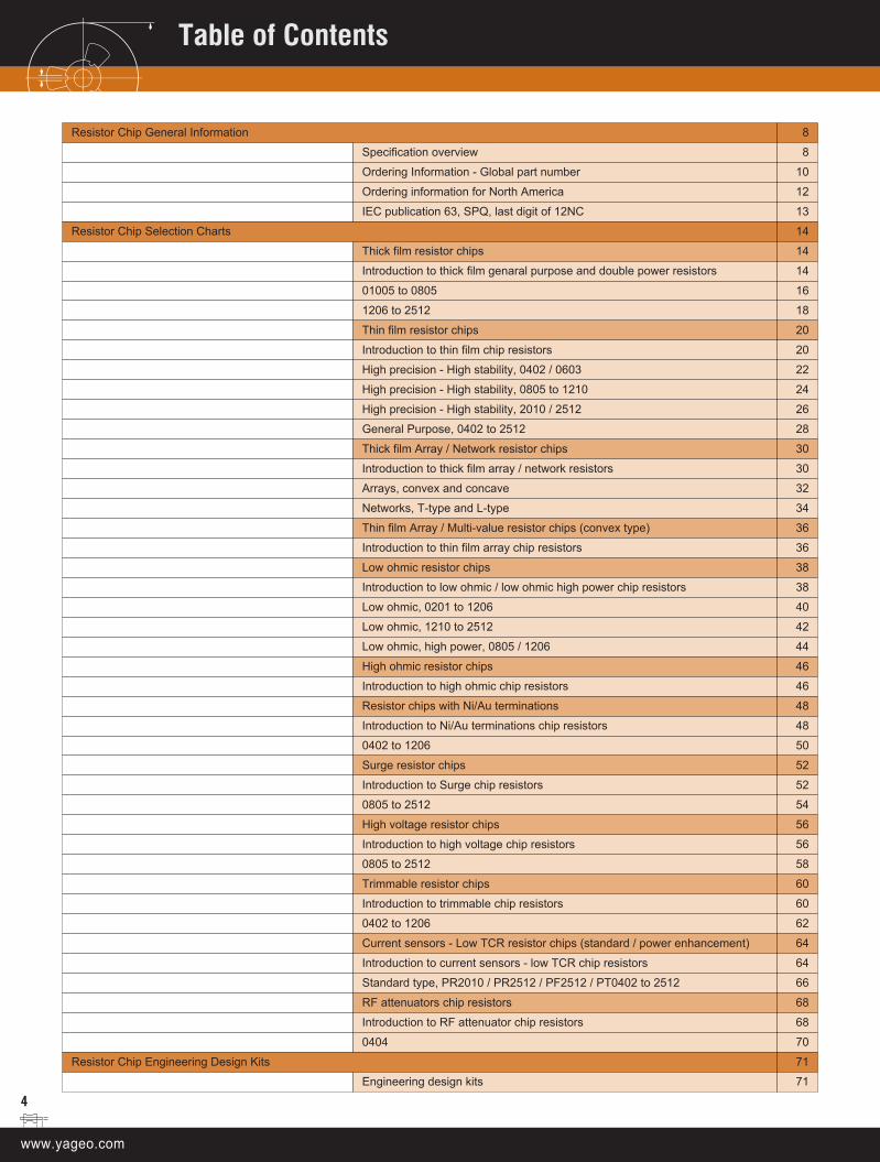
Resistor Chip General Information 8
Specification overview 8
Ordering Information - Global part number 10
Ordering information for North America 12
IEC publication 63, SPQ, last digit of 12NC 13
Resistor Chip Selection Charts 14
Thick film resistor chips 14
Introduction to thick film genaral purpose and double power resistors 14
01005 to 0805 16
1206 to 2512 18
Thin film resistor chips 20
Introduction to thin film chip resistors 20
High precision - High stability, 0402 / 0603 22
High precision - High stability, 0805 to 1210 24
High precision - High stability, 2010 / 2512 26
General Purpose, 0402 to 2512 28
Thick film Array / Network resistor chips 30
Introduction to thick film array / network resistors 30
Arrays, convex and concave 32
Networks, T-type and L-type 34
Thin film Array / Multi-value resistor chips (convex type) 36
Introduction to thin film array chip resistors 36
Low ohmic resistor chips 38
Introduction to low ohmic / low ohmic high power chip resistors 38
Low ohmic, 0201 to 1206 40
Low ohmic, 1210 to 2512 42
Low ohmic, high power, 0805 / 1206 44
High ohmic resistor chips 46
Introduction to high ohmic chip resistors 46
Resistor chips with Ni/Au terminations 48
Introduction to Ni/Au terminations chip resistors 48
0402 to 1206 50
Surge resistor chips 52
Introduction to Surge chip resistors 52
0805 to 2512 54
High voltage resistor chips 56
Introduction to high voltage chip resistors 56
0805 to 2512 58
Trimmable resistor chips 60
Introduction to trimmable chip resistors 60
0402 to 1206 62
Current sensors - Low TCR resistor chips (standard / power enhancement) 64
Introduction to current sensors - low TCR chip resistors 64
Standard type, PR2010 / PR2512 / PF2512 / PT0402 to 2512 66
RF attenuators chip resistors 68
Introduction to RF attenuator chip resistors 68
0404 70
Resistor Chip Engineering Design Kits 71
Engineering design kits 71
Table of Contents

5
MLCC General Information 74
Specification overview 74
Case dimensions 75
Ordering Information - Global part number 76
Ordering information for North America 77
Thickness classes and packing quantities for all series 78
MLCC Selection Charts 79
NP0 79
NP0 - General purpose 16 to 25V, 0201 to 0603 79
NP0 - General purpose 16 to 25V, 0805 to 1210 80
NP0 - Gerneral purpose 50V, 0201 to 1812 82
NP0 - Midium voltage, 0603 / 0805 85
NP0 - Midium voltage, 1206 / 1210 86
NP0 - Midium voltage, 1808 / 1812 87
NP0 - High voltage, 1206 / 1210 88
NP0 - High voltage, 1808 / 1812 89
NP0 - High frequency, 0402 / 0603 91
NP0 - Microwave, 0603 to 1206 93
X7R 95
X7R - General purpose, 0201 / 0402 95
X7R - General purpose & High capacitance, 0603 / 0805 96
X7R - Gerneral purpose & High capacitance, 1206 to 1812 97
X7R - Midium voltage, 0603 / 0805 98
X7R - Midium voltage, 1206 / 1210 99
X7R - Midium voltage, 1808 / 1812 100
X7R - High voltage, 1206 / 1210 101
X7R - High voltage, 1808 / 1812 102
X7R - Low inductance, 0306 to 0612 104
X5R 106
X5R - General purpose & High capacitance, 0201 / 0402 106
X5R - General purpose & High capacitance, 0603 / 0805 107
X5R - High capacitance, 1206 to 1812 108
Y5V 110
Y5V - General purpose & High capacitance, 0201 / 0402 110
Y5V - General purpose & High capacitance, 0603 / 0805 111
Y5V - General purpose & High capacitance, 1206 / 1210 112
Safety certification MLCCs 114
NP0 - High voltage SC type, 1808 / 1812 114
X7R - High voltage SC type, 1808 / 1812 115
Arrays 117
X7R - 2C Arrays, 0405 117
NP0 - 4C Arrays, 0508 / 0612 119
X7R - 4C Arrays, 0508 / 0612 120
Y5V - 4C Arrays, 0508 / 0612 121
MLCC Engineering Design Kits 123
Sample kits for 0201 / 0402 123
Sample kits for 0603 / 0805 124
Sample kits for 1206 125
Sample kits for high capacitance series 126
Table of Contents
6
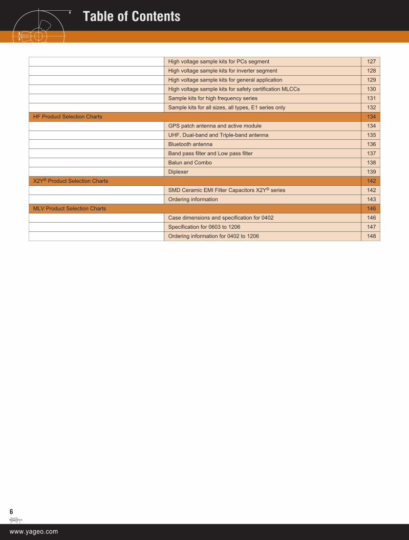
High voltage sample kits for PCs segment 127
High voltage sample kits for inverter segment 128
High voltage sample kits for general application 129
High voltage sample kits for safety certification MLCCs 130
Sample kits for high frequency series 131
Sample kits for all sizes, all types, E1 series only 132
HF Product Selection Charts 134
GPS patch antenna and active module 134
UHF, Dual-band and Triple-band antenna 135
Bluetooth antenna 136
Band pass filter and Low pass filter 137
Balun and Combo 138
Diplexer 139
X2Y® Product Selection Charts 142
SMD Ceramic EMI Filter Capacitors X2Y® series 142
Ordering information 143
MLV Product Selection Charts 146
Case dimensions and specification for 0402 146
Specification for 0603 to 1206 147
Ordering information for 0402 to 1206 148
Table of Contents
SURFACE-MOUNT RESISTOR CHIPS
8
T. C. R. - RL series
Type Operating Temp. range
Resistance range
T. C. R.50mΩ - 1Ω
RL0402 -55°C to +125°C 50mΩ≤R<1Ω ±800 ppm/°C10mΩ - 36mΩ 36mΩ - 91mΩ 91mΩ - 500mΩ 500mΩ - 1Ω
RL0603 -55°C to +125°C 10mΩ≤R<1Ω ±1 500 ppm/°C ±1 200 ppm/°C ±800 ppm/°C ±300 ppm/°C10mΩ - 18mΩ 20mΩ - 47mΩ 51mΩ - 91mΩ 100mΩ - 360mΩ 390mΩ - 500mΩ 510mΩ - 1Ω
RL0805 -55°C to +125°C 10mΩ≤R<1Ω ±1 500 ppm/°C ±1 200 ppm/°C ±1 000 ppm/°C ±600 ppm/°C ±300 ppm/°C ±200 ppm/°CRL1206 -55°C to +125°C 10mΩ≤R<1Ω ±1 500 ppm/°C ±1 200 ppm/°C ±1 000 ppm/°C ±600 ppm/°C ±300 ppm/°C ±200 ppm/°CRL1210 -55°C to +125°C 10mΩ≤R<1Ω ±1 500 ppm/°C ±1 000 ppm/°C ±800 ppm/°C ±600 ppm/°C ±300 ppm/°C ±200 ppm/°C
10mΩ - 30mΩ 33mΩ - 56mΩ 60mΩ - 180mΩ 200mΩ - 1ΩRL1218 -55°C to +125°C 10mΩ≤R<1Ω ±2 000 ppm/°C ±1 000 ppm/°C ±700 ppm/°C ±250 ppm/°C
10mΩ - 18mΩ 20mΩ - 47mΩ 51mΩ - 91mΩ 100mΩ - 360mΩ 390mΩ - 500mΩ 510mΩ - 1ΩRL2010 -55°C to +125°C 10mΩ≤R<1Ω ±1 500 ppm/°C ±1 200 ppm/°C ±1 000 ppm/°C ±600 ppm/°C ±300 ppm/°C ±200 ppm/°CRL2512 -55°C to +125°C 10mΩ ≤R<1Ω ±1 500 ppm/°C ±1 200 ppm/°C ±800 ppm/°C ±600 ppm/°C ±300 ppm/°C ±200 ppm/°C
Global part number Series Size Power rating
Max. voltage
Operating Temp. range
Resistance range Tolerance T. C. R.
! RC0100xR-07xxxxL
RC
01005 1/32W 15V -55°C to 125°C 10Ω≤ R ≤1MΩ ±5% 10Ω≤ R ≤1MΩ ±250 ppm/°C
RC0201xR-07xxxxL 0201 1/20W 25V -55°C to 125°C 1Ω≤ R ≤10MΩ Max.: 1MΩ ±1%Max.: 10MΩ ±5%
1Ω≤ R ≤10Ω 10Ω< R ≤10MΩ
-100/+350 ppm/°C±200 ppm/°C
RC0402xR-07xxxxL 0402 1/16W 50V -55°C to 155°C 1Ω≤ R ≤22MΩ
Max./Min.: 1MΩ/10Ω ±0.5% Max.: 10MΩ ±1% Max.: 22MΩ ±5%
1Ω≤ R ≤10Ω10MΩ< R ≤22MΩ ±200 ppm/°C
RC0603xR-07xxxxL 0603 1/10W 50V -55°C to 155°C 1Ω≤ R ≤22MΩ RC0805xR-07xxxxL 0805 1/8W 150V -55°C to 155°C 1Ω≤ R ≤22MΩ RC1206xR-07xxxxL 1206 1/4W 200V -55°C to 155°C 1Ω≤ R ≤22MΩ RC1210xR-07xxxxL 1210 1/2W 200V -55°C to 155°C 1Ω≤ R ≤22MΩ 10Ω< R ≤10MΩ ±100 ppm/°C RC1218xK-07xxxxL 1218 1W 200V -55°C to 155°C 1Ω≤ R ≤1MΩ RC2010xK-07xxxxL 2010 3/4W 200V -55°C to 155°C 1Ω≤ R ≤22MΩ RC2512xK-07xxxxL 2512 1W 200V -55°C to 155°C 1Ω≤ R ≤22MΩ! RC0805xR-7WxxxxL 0805 1/4W 150V -55°C to 155°C 1Ω≤ R ≤100Ω
±1%±5% ±200 ppm/°C! RC1206xR-7WxxxxL 1206 1/2W 200V -55°C to 155°C 1Ω≤ R ≤100Ω
! RC2512xK-7WxxxxL 2512 2W 200V -55°C to 155°C 1Ω≤ R ≤150Ω! RC0805xR-07xxxxL 0805 1/8W 150V -55°C to 155°C 24MΩ≤ R ≤100MΩ
±5%, ±10%, ±20% ±300 ppm/°C! RC1206xR-07xxxxL 1206 1/4W 200V -55°C to 155°C 24MΩ≤ R ≤100MΩ! YC102-xR-07xxxxL
YC
2*0201 1/32W 15V -55°C to 125°C 10Ω≤ R ≤1MΩMin.: 10Ω ±1%Min.: 1Ω ±5%
±200 ppm/°C
YC122-xR-07xxxxL 2*0402 1/16W 50V -55°C to 125°C 1Ω≤ R ≤1MΩ YC124-xR-07xxxxL 4*0402 1/16W 50V -55°C to 155°C 10Ω≤ R ≤1MΩ! YC162-xR-07xxxxL 2*0603 1/16W 50V -55°C to 155°C 10Ω≤ R ≤1MΩ ±5% YC164-xR-07xxxxL 4*0603 1/16W 50V -55°C to 155°C 1Ω≤ R ≤1MΩ
±1%±5% YC248-xR-07xxxxL 8*0602 1/16W 50V -55°C to 155°C 10Ω≤ R ≤1MΩ
YC324-xR-07xxxxL 4*1206 1/8W 200V -55°C to 155°C 10Ω≤ R ≤1MΩ! TC122-xR-07xxxxL
TC2*0402 1/16W 25V -55°C to 125°C 10Ω≤ R ≤1MΩ
Min.: 10Ω ±1%Min.: 1Ω ±5%! TC124-xR-07xxxxL 4*0402 1/16W 50V -55°C to 125°C 10Ω≤ R ≤1MΩ
TC164-xR-07xxxxL 4*0603 1/16W 50V -55°C to 155°C 1Ω≤ R ≤1MΩ
YC158TJR-07xxxxL YC158 10P8R (0612) 1/16W 25V -55°C to 155°C 10Ω≤ R ≤100KΩ ±5% 10Ω≤ R ≤100KΩ ±200 ppm/°C
YC358xJK-07xxxxL YC358 10P8R (1225) 1/16W 50V -55°C to 155°C 10Ω≤ R ≤330KΩ ±5% 10Ω≤ R ≤330KΩ ±200 ppm/°C
RL0402xR-07xxxxL
RL
0402 1/16W (PxR)^1/2 -55°C to 125°C 0.05Ω≤ R <1Ω
±1%±2%±5%
See following table “T.C.R.- RL series“
RL0603xR-07xxxxL 0603 1/10W (PxR)^1/2 -55°C to 125°C
0.01Ω≤ R <1Ω
RL0805xR-07xxxxL 0805 1/8W (PxR)^1/2 -55°C to 125°C RL1206xR-07xxxxL 1206 1/4W (PxR)^1/2 -55°C to 125°C RL1210xR-07xxxxL 1210 1/2W (PxR)^1/2 -55°C to 125°C RL1218xK-07xxxxL 1218 1W (PxR)^1/2 -55°C to 125°C RL2010xK-07xxxxL 2010 3/4W (PxR)^1/2 -55°C to 125°C RL2512xK-07xxxxL 2512 1W (PxR)^1/2 -55°C to 125°C! RL0805xR-7WxxxxL 0805 1/4W (PxR)^1/2 -55°C to 125°C
0.01Ω≤ R <1Ω! RL1206xR-7WxxxxL 1206 1/2W (PxR)^1/2 -55°C to 125°C
Note: " ! " is the symbol for new product
Resistor Chip General InformationSpecification overview
9
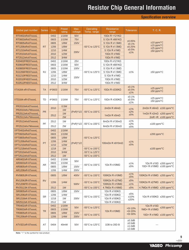
Global part number Series Size Power rating
Max. voltage
Operating Temp. range
Resistance range Tolerance T. C. R.
RT0402xRx07xxxxL
RT
0402 1/16W 50V
-55°C to 125°C
10Ω≤ R <121KΩ
±0.05%±0.1%
±0.25% ±0.5% ±1%
±10 ppm/°C±15 ppm/°C±25 ppm/°C±50 ppm/°C
RT0603xRx07xxxxL 0603 1/10W 75V 5.1Ω≤ R ≤681KΩ RT0805xRx07xxxxL 0805 1/8W 150V 5.1Ω≤ R ≤1.5MΩ RT1206xRx07xxxxL 1206 1/8W
200V
5.1Ω≤ R ≤1.5MΩ RT1210xRx07xxxxL 1210 1/4W 5.1Ω≤ R ≤1MΩ RT2010xKx07xxxxL 2010 1/2W 10Ω≤ R ≤1MΩ RT2512xKx07xxxxL 2512 3/4W 10Ω≤ R ≤1MΩ RJ0402FRE07xxxxL
RJ
0402 1/16W 25V
-55°C to 125°C
10Ω≤ R ≤121KΩ
±1% ±50 ppm/°C
RJ0603FRE07xxxxL 0603 1/16W 50V 5.1Ω≤ R ≤681KΩ RJ0805FRE07xxxxL 0805 1/10W 100V 5.1Ω≤ R ≤1.5MΩ RJ1206FRE07xxxxL 1206 1/8W
150V
5.1Ω≤ R ≤1.5MΩ RJ1210FRE07xxxxL 1210 1/4W 5.1Ω≤ R ≤1MΩ RJ2010FKE07xxxxL 2010 1/2W 10Ω≤ R ≤1MΩ RJ2512FKE07xxxxL 2512 3/4W 10Ω≤ R ≤1MΩ
! TA164-xR-07xxxxL TA 4*0603 1/16W 75V -55°C to 125°C 10Ω≤ R ≤330KΩ±0.1%±0.5%±1%
±25 ppm/°C±50 ppm/°C
! TD164-xR-07xxxxL TD 4*0603 1/16W 75V -55°C to 125°C 10Ω≤ R ≤330KΩ±0.1%±0.5%±1%
±25 ppm/°C ±50 ppm/°C
PR2010xKx07xxxxxL
PR2010
0.5W
(PxR)^1/2 -55°C to 155°C2mΩ≤ R ≤6mΩ ±1%
±2%±5%
2mΩ≤ R ≤6mΩ ±150 ppm/°C PR2010xKx7WxxxxxL 1W PR2512xKx07xxxxxL
25121W
1mΩ≤ R ≤5mΩ1mΩ≤ R ≤2mΩ ±200 ppm/°C
PR2512xKx7WxxxxxL 2W 2mR <R ±100 ppm/°C
PF2512xKx07xxxxxLPF
2512 1W(PxR)^1/2 -55°C to 155°C
6mΩ≤ R ≤130mΩ ±1%±2%±5%
±100 ppm/°C PF2512xKx7WxxxxxL 2512 2W 6mΩ≤ R ≤130mΩ
! PT0402xRx07xxxxL
PT
0402 1/16W
(PxR)^1/2
-55°C to 125°C
100mΩ≤ R ≤910mΩ ±1%±5%
±200 ppm/°C! PT0603xRx07xxxxL 0603 1/10W! PT0805xRx07xxxxL 0805 1/8W! PT1206xRx07xxxxL 1206 1/4W
±100 ppm/°C! PT1210xRx07xxxxL 1210 1/2W! PT1218xKx07xxxxL 1218 1W -55°C to 155°C! PT2010xKx07xxxxL 2010 3/4W -55°C to 125°C! PT2512xKx07xxxxL 2512 1W -55°C to 155°C AR0402xR-07xxxxL
AR
0402 1/16W50V
-55°C to 155°C 1Ω≤ R ≤10MΩ ±1%±5%
1Ω≤ R ≤10Ω10Ω< R ≤10MΩ
±200 ppm/°C±100 ppm/°C
AR0603xR-07xxxxL 0603 1/10W AR0805xR-07xxxxL 0805 1/8W 150V AR1206xR-07xxxxL 1206 1/4W 200V
RV0805JR-07xxxxL
RV
0805 1/8W 400V -55°C to 155°C 100KΩ≤ R ≤10MΩ ±1%±5% 100KΩ≤ R ≤10MΩ ±200 ppm/°C
RV1206JR-07xxxxL1206 1/4W
500V-55°C to 155°C
100KΩ≤ R ≤27MΩ ±5%100KΩ≤ R ≤27MΩ ±200 ppm/°C
RV1206FR-07xxxxL 100KΩ≤ R ≤10MΩ ±1% RV2512JK-07xxxxL 2512 1W -55°C to 155°C 4.7MΩ≤ R ≤16MΩ ±5% 4.7MΩ≤ R ≤16MΩ ±200 ppm/°C SR0805xR-07xxxxL
SR
0805 1/8W 150V
-55°C to 155°C
1Ω≤ R ≤100KΩ±5%
±10%±20%
1Ω≤ R ≤100KΩ ±200 ppm/°C SR1206xR-07xxxxL 1206 1/4W
200V1Ω≤ R ≤100KΩ
SR1218xK-07xxxxL 1218 1W 1Ω≤ R ≤100KΩ SR2512xK-07xxxxL 2512 1W 1Ω≤ R ≤100KΩ TR0402xR-07xxxxL
TR
0402 1/16W50V -55°C to 125°C
1Ω≤ R ≤10MΩ+0/-10% +0/-20% +0/-30%
1Ω≤ R ≤10Ω±200 ppm/°C
TR0603xR-07xxxxL 0603 1/16W 1MΩ< R ≤10MΩ TR0805xR-07xxxxL 0805 1/8W 150V
-55°C to 155°C 10Ω< R ≤1MΩ ±100 ppm/°C TR1206xR-07xxxxL 1206 1/4W 200V
ATV321xR-07xxxxL AT 0404 40mW 50V -55°C to 125°C 1DB to 20D B
±0.3dB ±0.5dB ±1.0dB ±2.0dB
---
Note: " ! " is the symbol for new product
Resistor Chip General InformationSpecification overview
10
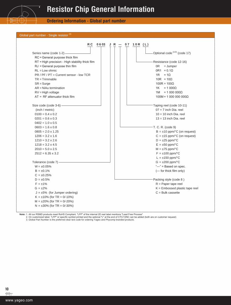
Global part number - Single resistor (3)
R C 0 6 03 J R ― 0 7 1 0 R ( L )
Series name (code 1-2) Optional code (1/2) (code 17) RC = General purpose thick film RT = High precision - High stability thick film Resistance (code 12-16) RJ = General purpose thin film 0R = Jumper RL = Low ohmic 0R1 = 0.1Ω PR / PF / PT = Current sensor - low TCR 1R = 1Ω TR = Trimmable 10R = 10Ω SR = Surge 100R = 100Ω AR = NiAu termination 1K = 1 000Ω RV = High voltage 1M = 1 000 000ΩAT = RF attenuator thick film 100M = 1 000 000 000Ω
Size code (code 3-6) Taping reel (code 10-11)
(inch / metric) 07 = 7 inch Dia. reel0100 = 0.4 x 0.2 10 = 10 inch Dia. reel0201 = 0.6 x 0.3 13 = 13 inch Dia. reel0402 = 1.0 x 0.50603 = 1.6 x 0.8 T. C. R. (code 9)0805 = 2.0 x 1.25 B = ±10 ppm/°C (on request)1206 = 3.2 x 1.6 C = ±15 ppm/°C (on request)1210 = 3.2 x 2.6 D = ±25 ppm/°C1218 = 3.2 x 4.5 E = ±50 ppm/°C2010 = 5.0 x 2.5 M = ±75 ppm/°C2512 = 6.35 x 3.2 F = ±100 ppm/°C
L = ±150 ppm/°CTolerance (code 7) G = ±200 ppm/°C
W = ±0.05% “―” = Based on spec. B = ±0.1% (― for thick film only)
C = ±0.25% D = ±0.5% Packing style (code 8 ) F = ±1% R = Paper tape reel G = ±2% K = Embossed plastic tape reel J = ±5% (for Jumper ordering) C = Bulk cassette K = ±10% (for TR = 0/-10%) M = ±20% (for TR = 0/-20%) N = ±30% (for TR = 0/-30%)
Note: 1. All our RSMD products meet RoHS Compliant. "LFP" of the internal 2D reel label mentions "Lead Free Process" 2. On customized label. "LFP" or specific symbol printed and the optional "L" at the end of CTC/12NC can be added (both are on customer request) 3. Global Part Number is the preferred clear text code for ordering Yageo and Phycomp branded products.
Resistor Chip General InformationOrdering Information - Global part number

11
Global part number - Power enhancement
R L 0 8 0 5 J R ― 7 W 0 R 0 1 5 ( L )
Series name (code 1-2) Optional code (code 17) RC = General purpose thick film RL = Low ohmic Resistance (code 12-16) PR / PF / PT = Current sensor - low TCR 0R01 = 0.01Ω
0R1 = 0.1ΩSize code (code 3-6) 1R = 1Ω
(inch / metric) 10R = 10Ω0805 = 2.0 x 1.25 100R = 100Ω1206 = 3.2 x 1.6 1K = 1 000Ω2010 = 5.0 x 2.5 1M = 1 000 000Ω2512 = 6.35 x 3.2
Power rating (code 11)Tolerance (code 7) W = 2 x standard power
F = ±1% G = ±2% Taping reel (code 10) J = ±5% 7 = 7 inch Dia. reel
Packing style (code 8 ) T. C. R. (code 9)R = Paper tape reel M = ±75 ppm/°CK = Embossed plastic tape reel F = ±100 ppm/°C
G = ±200 ppm/°C“―” = Based on spec.(― for thick film only)
Global part number - Arrays & Networks
Y C 1 6 4 ― J R ― 0 7 1 0 R ( L )
Series name (code 1-2) Optional code (code 17) YC = Aarray & Network (convex) thick filmTC = Array (concave) thick film Resistance (code 12-16)TA = Array (convex) thin film 0R = JumperTD = Multi value array (convex) thin film 0R1 = 0.1Ω 1R = 1Ω
Size code (inch) (code 3-4) 10R = 10Ω10 = 0201 x 2 (0202) 100R = 100Ω12 = 0402 x 2 (0404) 1K = 1 000Ω 0402 x 4 (0408) 1M = 1 000 000Ω15 = 10Pin/8R (0612)16 = 0603 x 2 (0606) Taping reel (code 10-11) 0603 x 4 (0612) 07 = 7 inch Dia. reel24 = 0602 x 8 (0616) 10 = 10 inch Dia. reel32 = 1206 x 4 (1224) 13 = 13 inch Dia. reel35 = 10Pin/8R (1225)
T.C.R. (code 9)Number of resistors (code 5) D = ±25 ppm/°C
2 = 2 resistors E = ±50 ppm/°C4 = 4 resistors "―" = Based on spec.8 = 8 resistors
Packing style (code 8 )Schematic (code 6) R = Paper tape reel
L = L-type (for YC358) K = Embossed plastic tape reelT = T-type (for YC158/358)“―” = Based on spec. Tolerance (code 7)
B = ±0.1%D = ±0.5%F = ±1%J = ±5% (for Jumper ordering)
Resistor Chip General InformationOrdering Information - Global part number

12
Phycomp CTC ordering code - Noth America
Ordering example: 9C06031A10R0FKHFT = R-chip 0603, 10R0, 1%, 5K reel
1-2 3-6 7-8 9-12 13 14 15-16 17X X X X X X X X X X X X X X X X X
Series name (code 1-2) Packing style (code 17 ) 9C = Phycomp Thick film chip resistors T = 5K paper 9T = Phycomp Thin film chip resistors 3 = 10K paper
4 = 20K paperSize code (standard resistors, code 3-6) 5 = 4K blister
0201 0201 (0603) 6 = 5K blister0402 0402 (1005) 7 = 50K paper0603 0603 (1608) P = 25K bulk case0805 0805 (2012)1206 1206 (3216) Special coding (code 15-16)1210 1210 (3225) HF = SnPb1218 1218 (3248) PF = Lead free2010 2010 (5025) AF = NiAu2512 2512 (6432)AC34 0603 (1608) 4R concave array T.C.R. (code 14)AV34 0603 (1608) 4R convex array C = ±10 ppm/°CAV22 0402 (1005) 2R convex array D = ±15 ppm/°CAV24 0402 (1005) 4R convex array A = ±25 ppm/°CAV28 0402 (1005) 8R convex array B = ±50 ppm/°CRN31 10P8R in 1206 convex network K = ±100 ppm/°CFR01 1206 (3216) Fusible L = ±200 ppm/°CFR21 0603 (1608) Fusible E = ±250 ppm/°CSR01 1206 (3216) Surge M = ±300 ppm/°CVR01 1206 (3216) High voltage 5% G = ±500 ppm/°CVR02 1206 (3216) High voltage 1% F = 0/+500 ppm/°CVR11 0805 (2012) High voltage 5% R = ±600 ppm/°CVR12 0805 (2012) High voltage 1% Q = -100/+600 ppm/°C
VR21 2512 (6432) High voltage 5% P = ±750 ppm/°CMR22 2512 (6432) Current sensor - low TCR H = ±1000 ppm/°CMF22 2512 (6432) Current sensor - low TCR I = ±1500 ppm/°CV321 0404 (1010) RF attenuator J = ±2000 ppm/°C
N = ±3000 ppm/°CPower rating (code 7-8)
1A 1/16W 0.063W 90402 Tolerance (code 13)1A 1/10W 0.10W (0603 E = ±0.01%2A 1/8W 0.125W (0805) A = ±0.05%3A 1/4W 0.25W (1206) B = ±0.1%; 0.2dB5A 1/2W 0.5W (1210) C = ±0.25%; 0.3dB7A 1/20W 0.05W (0201) D = ±0.5%; 0.5dB8A 1/32W 0.03125W (RN31) F = ±1%; 1dB12 3/4W 0.75W (2010) G = ±2%; 2dB1W 1W 1W (1218/2512) J = ±5%2W 2W 2W N = 0/-20%
R = 0/-30%Resistance valre (code 9-12)
0R00 = JumperR0XX < 0.1ΩRXXX = 0.1Ω - 0.976ΩXRXX = 1Ω - 9.76ΩXXRX = 10Ω - 97.6ΩXXX0 = 100Ω - 976ΩXXX1 = 1K - 9.76KXXX2 = 10K - 97.6KXXX3 = 100K - 9.78KXXX4 = 1M - 9.76MXXX5 = 10M - 97.6MXXX6 = 100M+XXDB = 1 - 20DB
Right values apply to trimmable resistors
dB values apply to Attenuators
Resistor Chip General InformationOrdering information for North America
13
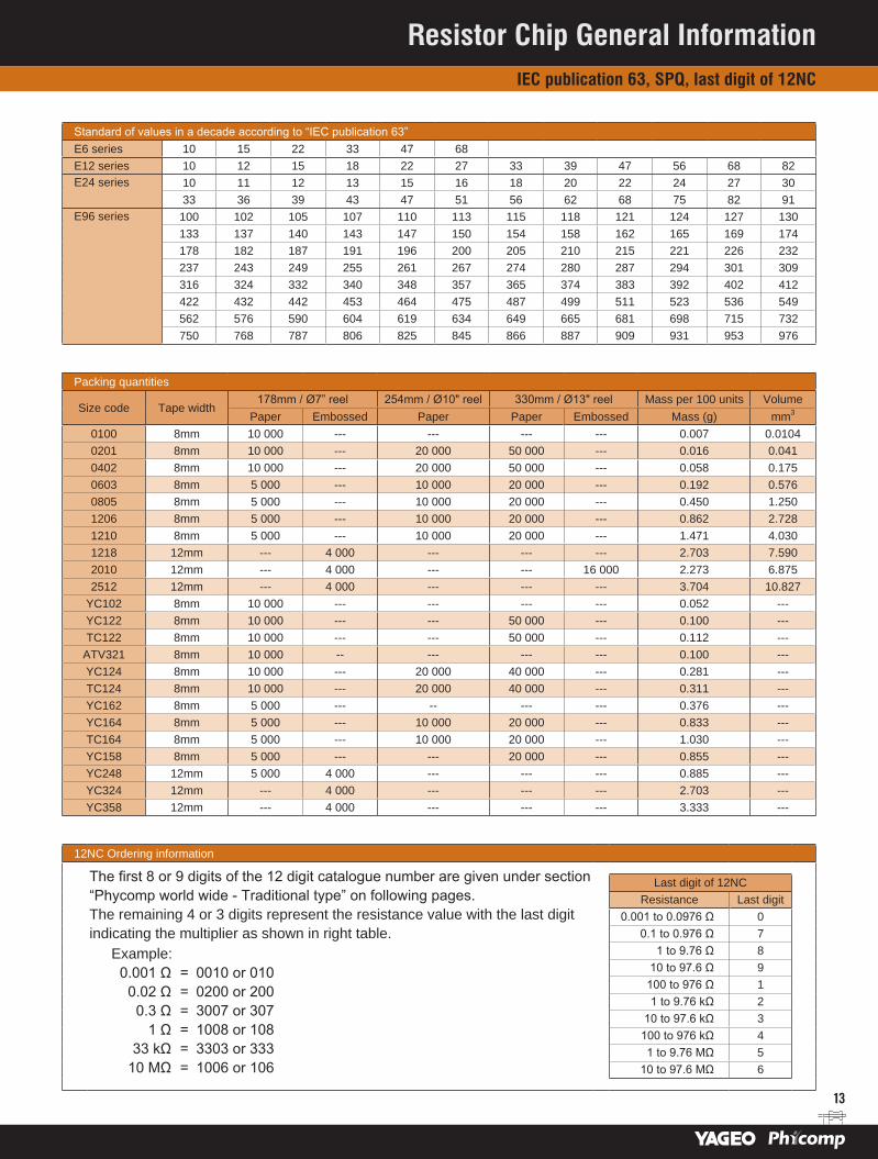
Standard of values in a decade according to “IEC publication 63”E6 series 10 15 22 33 47 68E12 series 10 12 15 18 22 27 33 39 47 56 68 82E24 series 10 11 12 13 15 16 18 20 22 24 27 30
33 36 39 43 47 51 56 62 68 75 82 91E96 series 100 102 105 107 110 113 115 118 121 124 127 130
133 137 140 143 147 150 154 158 162 165 169 174178 182 187 191 196 200 205 210 215 221 226 232237 243 249 255 261 267 274 280 287 294 301 309316 324 332 340 348 357 365 374 383 392 402 412422 432 442 453 464 475 487 499 511 523 536 549562 576 590 604 619 634 649 665 681 698 715 732750 768 787 806 825 845 866 887 909 931 953 976
Packing quantities
Size code Tape width178mm / Ø7” reel 254mm / Ø10" reel 330mm / Ø13" reel Mass per 100 units Volume
Paper Embossed Paper Paper Embossed Mass (g) mm3
0100 8mm 10 000 --- --- --- --- 0.007 0.01040201 8mm 10 000 --- 20 000 50 000 --- 0.016 0.0410402 8mm 10 000 --- 20 000 50 000 --- 0.058 0.1750603 8mm 5 000 --- 10 000 20 000 --- 0.192 0.5760805 8mm 5 000 --- 10 000 20 000 --- 0.450 1.2501206 8mm 5 000 --- 10 000 20 000 --- 0.862 2.7281210 8mm 5 000 --- 10 000 20 000 --- 1.471 4.0301218 12mm --- 4 000 --- --- --- 2.703 7.5902010 12mm --- 4 000 --- --- 16 000 2.273 6.8752512 12mm --- 4 000 --- --- --- 3.704 10.827
YC102 8mm 10 000 --- --- --- --- 0.052 ---YC122 8mm 10 000 --- --- 50 000 --- 0.100 ---TC122 8mm 10 000 --- --- 50 000 --- 0.112 ---
ATV321 8mm 10 000 -- --- --- --- 0.100 ---YC124 8mm 10 000 --- 20 000 40 000 --- 0.281 ---TC124 8mm 10 000 --- 20 000 40 000 --- 0.311 ---YC162 8mm 5 000 --- -- --- --- 0.376 ---YC164 8mm 5 000 --- 10 000 20 000 --- 0.833 ---TC164 8mm 5 000 --- 10 000 20 000 --- 1.030 ---YC158 8mm 5 000 --- --- 20 000 --- 0.855 ---YC248 12mm 5 000 4 000 --- --- --- 0.885 ---YC324 12mm --- 4 000 --- --- --- 2.703 ---YC358 12mm --- 4 000 --- --- --- 3.333 ---
12NC Ordering information
The first 8 or 9 digits of the 12 digit catalogue number are given under section “Phycomp world wide - Traditional type” on following pages. The remaining 4 or 3 digits represent the resistance value with the last digit indicating the multiplier as shown in right table.
Last digit of 12NCResistance Last digit
0.001 to 0.0976 Ω 00.1 to 0.976 Ω 7
Example: 0.001 Ω = 0010 or 010 0.02 Ω = 0200 or 200 0.3 Ω = 3007 or 307 1 Ω = 1008 or 108 33 kΩ = 3303 or 333 10 MΩ = 1006 or 106
1 to 9.76 Ω 8 10 to 97.6 Ω 9
100 to 976 Ω 11 to 9.76 kΩ 2
10 to 97.6 kΩ 3100 to 976 kΩ 41 to 9.76 MΩ 5
10 to 97.6 MΩ 6
Resistor Chip General InformationIEC publication 63, SPQ, last digit of 12NC
14
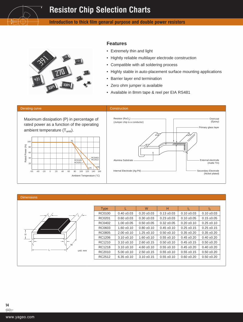
FeaturesExtremely thin and light
Hightly reliable multilayer electrode construction
Compatible with all soldering process
Highly stable in auto-placement surface mounting applications
Barrier layer end termination
Zero ohm jumper is available
Available in 8mm tape & reel per EIA RS481
•
•
•
•
•
•
•
Derating curve Construction
Maximum dissipation (P) in percentage of rated power as a function of the operating ambient temperature (Tamb).
100
80
60
40
20
-55 -40 -20 0 20 40 60 80
70
100 120 140 160
Ambient Temperature (°C)
Rat
ed P
ower
(%)
155
RC0402-RC2512
125
RC0100-RC0201
Overcoat(Epoxy)
Primary glass layer
Secondary Electrode (Nickel plated)
External electrode(matte Tin)
Resistor (RuO2)
(Jumper chip is a conductor)
Alumina Substrate
Internal Electrode (Ag-Pd)
Dimensions
W
unit: mm
I2
I2
I1
I1
L
H
Type L W H I1 I2RC0100 0.40 ±0.03 0.20 ±0.03 0.13 ±0.03 0.10 ±0.03 0.10 ±0.03RC0201 0.60 ±0.03 0.30 ±0.03 0.23 ±0.03 0.10 ±0.05 0.15 ±0.05RC0402 1.00 ±0.05 0.50 ±0.05 0.32 ±0.05 0.20 ±0.10 0.25 ±0.10RC0603 1.60 ±0.10 0.80 ±0.10 0.45 ±0.10 0.25 ±0.15 0.25 ±0.15RC0805 2.00 ±0.10 1.25 ±0.10 0.50 ±0.10 0.35 ±0.20 0.35 ±0.20RC1206 3.10 ±0.10 1.60 ±0.10 0.55 ±0.10 0.45 ±0.20 0.40 ±0.20RC1210 3.10 ±0.10 2.60 ±0.15 0.50 ±0.10 0.45 ±0.15 0.50 ±0.20RC1218 3.10 ±0.10 4.60 ±0.10 0.55 ±0.10 0.45 ±0.20 0.40 ±0.20RC2010 5.00 ±0.10 2.50 ±0.15 0.55 ±0.10 0.55 ±0.15 0.50 ±0.20RC2512 6.35 ±0.10 3.10 ±0.15 0.55 ±0.10 0.60 ±0.20 0.50 ±0.20
Resistor Chip Selection ChartsIntroduction to thick film genaral purpose and double power resistors
15
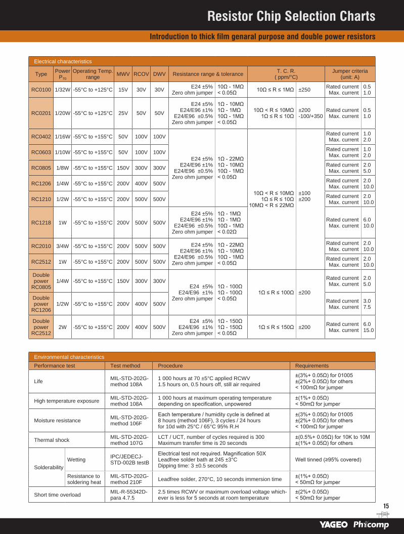
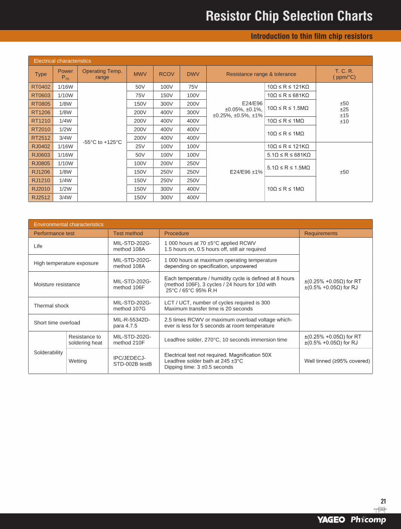
Electrical characteristics
Type Power P70
Operating Temp. range MWV RCOV DWV Resistance range & tolerance T. C. R.
( ppm/°C)Jumper criteria
(unit: A)
RC0100 1/32W -55°C to +125°C 15V 30V 30V E24 ±5% Zero ohm jumper
10Ω - 1MΩ < 0.05Ω 10Ω ≤ R ≤ 1MΩ ±250 Rated current
Max. current 0.5 1.0
RC0201 1/20W -55°C to +125°C 25V 50V 50V
E24 ±5% E24/E96 ±1%
E24/E96 ±0.5% Zero ohm jumper
1Ω - 10MΩ 1Ω - 1MΩ 10Ω - 1MΩ < 0.05Ω
10Ω < R ≤ 10MΩ 1Ω ≤ R ≤ 10Ω
±200 -100/+350
Rated current Max. current
0.5 1.0
RC0402 1/16W -55°C to +155°C 50V 100V 100V
E24 ±5% E24/E96 ±1%
E24/E96 ±0.5% Zero ohm jumper
1Ω - 22MΩ 1Ω - 10MΩ 10Ω - 1MΩ < 0.05Ω
10Ω < R ≤ 10MΩ 1Ω ≤ R ≤ 10Ω
10MΩ < R ≤ 22MΩ
±100 ±200
Rated current Max. current
1.0 2.0
RC0603 1/10W -55°C to +155°C 50V 100V 100V Rated current Max. current
1.0 2.0
RC0805 1/8W -55°C to +155°C 150V 300V 300V Rated current Max. current
2.0 5.0
RC1206 1/4W -55°C to +155°C 200V 400V 500V Rated current Max. current
2.0 10.0
RC1210 1/2W -55°C to +155°C 200V 500V 500V Rated current Max. current
2.0 10.0
RC1218 1W -55°C to +155°C 200V 500V 500V
E24 ±5% E24/E96 ±1%
E24/E96 ±0.5% Zero ohm jumper
1Ω - 1MΩ 1Ω - 1MΩ 10Ω - 1MΩ < 0.02Ω
Rated current Max. current
6.0 10.0
RC2010 3/4W -55°C to +155°C 200V 500V 500V E24 ±5% E24/E96 ±1%
E24/E96 ±0.5% Zero ohm jumper
1Ω - 22MΩ 1Ω - 10MΩ 10Ω - 1MΩ < 0.05Ω
Rated current Max. current
2.0 10.0
RC2512 1W -55°C to +155°C 200V 500V 500V Rated current Max. current
2.0 10.0
Double power
RC08051/4W -55°C to +155°C 150V 300V 300V
E24 ±5% E24/E96 ±1%
Zero ohm jumper
1Ω - 100Ω 1Ω - 100Ω < 0.05Ω
1Ω ≤ R ≤ 100Ω ±200
Rated current Max. current
2.0 5.0
Double power
RC12061/2W -55°C to +155°C 200V 400V 500V Rated current
Max. current 3.0 7.5
Double power
RC25122W -55°C to +155°C 200V 400V 500V
E24 ±5% E24/E96 ±1%
Zero ohm jumper
1Ω - 150Ω 1Ω - 150Ω < 0.05Ω
1Ω ≤ R ≤ 150Ω ±200 Rated current Max. current
6.0 15.0
Environmental characteristicsPerformance test Test method Procedure Requirements
Life MIL-STD-202G-method 108A
1 000 hours at 70 ±5°C applied RCWV 1.5 hours on, 0.5 hours off, still air required
±(3%+ 0.05Ω) for 01005 ±(2%+ 0.05Ω) for others < 100mΩ for jumper
High temperature exposure MIL-STD-202G-method 108A
1 000 hours at maximum operating temperature depending on specification, unpowered
±(1%+ 0.05Ω) < 50mΩ for jumper
Moisture resistance MIL-STD-202G-method 106F
Each temperature / humidity cycle is defined at 8 hours (method 106F), 3 cycles / 24 hours for 10d with 25°C / 65°C 95% R.H
±(3%+ 0.05Ω) for 01005 ±(2%+ 0.05Ω) for others < 100mΩ for jumper
Thermal shock MIL-STD-202G-method 107G
LCT / UCT, number of cycles required is 300 Maximum transfer time is 20 seconds
±(0.5%+ 0.05Ω) for 10K to 10M ±(1%+ 0.05Ω) for others
Solderability Wetting IPC/JEDECJ-
STD-002B testB
Electrical test not required. Magnification 50X Leadfree solder bath at 245 ±3°C Dipping time: 3 ±0.5 seconds
Well tinned (≥95% covered)
Resistance to soldering heat
MIL-STD-202G-method 210F Leadfree solder, 270°C, 10 seconds immersion time ±(1%+ 0.05Ω)
< 50mΩ for jumper
Short time overload MIL-R-55342D-para 4.7.5
2.5 times RCWV or maximum overload voltage which-ever is less for 5 seconds at room temperature
±(2%+ 0.05Ω)< 50mΩ for jumper
Resistor Chip Selection ChartsIntroduction to thick film genaral purpose and double power resistors

16
General Purpose thick film / RC seriesSize: inch (mm) 0201 (0603) 0402 (1005) 0603 (1608) 0805 (2012)Power P70 1/20W 1/16W 1/10W 1/8WTolerance ±5% ±1% ±5% ±1% ±5% ±1% ±5% ±1%Resistance Range E24 E24/E96 E24 E24/E96 E24 E24/E96 E24 E24/E96
Jumper1 Ω
1.5 Ω2.2 Ω3.3 Ω4.7 Ω6.8 Ω10 Ω15 Ω22 Ω33 Ω47 Ω68 Ω
100 Ω150 Ω220 Ω330 Ω470 Ω680 Ω
1 kΩ1.5 kΩ2.2 kΩ3.3 kΩ4.7 kΩ6.8 kΩ10 kΩ15 kΩ22 kΩ33 kΩ47 kΩ68 kΩ
100 kΩ150 kΩ220 kΩ330 kΩ470 kΩ680 kΩ
1 MΩ1.5 MΩ2.2 MΩ3.3 MΩ4.7 MΩ6.8 MΩ10 MΩ15 MΩ22 MΩ
Remark
Note: Products with lead free terminations meet RoHS requirements. None of the forbidden materials are used in products / production. The Pb-glass contained in electrodes, resistorelement and glass is exempted by RoHS.
Resistor Chip Selection Charts01005 to 0805
17
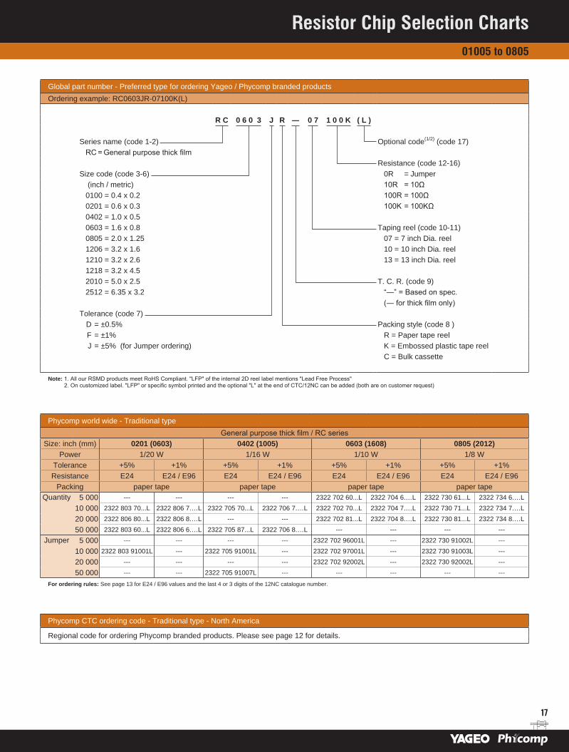
Global part number - Preferred type for ordering Yageo / Phycomp branded productsOrdering example: RC0603JR-07100K(L)
R C 0 6 0 3 J R ― 0 7 1 0 0 K ( L )
Series name (code 1-2) Optional code(1/2) (code 17) RC = General purpose thick film
Resistance (code 12-16)Size code (code 3-6) 0R = Jumper
(inch / metric) 10R = 10Ω0100 = 0.4 x 0.2 100R = 100Ω0201 = 0.6 x 0.3 100K = 100KΩ0402 = 1.0 x 0.50603 = 1.6 x 0.8 Taping reel (code 10-11)0805 = 2.0 x 1.25 07 = 7 inch Dia. reel1206 = 3.2 x 1.6 10 = 10 inch Dia. reel1210 = 3.2 x 2.6 13 = 13 inch Dia. reel1218 = 3.2 x 4.52010 = 5.0 x 2.5 T. C. R. (code 9)2512 = 6.35 x 3.2 “―” = Based on spec.
(― for thick film only)Tolerance (code 7)
D = ±0.5% Packing style (code 8 ) F = ±1% R = Paper tape reel J = ±5% (for Jumper ordering) K = Embossed plastic tape reel
C = Bulk cassette
Note: 1. All our RSMD products meet RoHS Compliant. "LFP" of the internal 2D reel label mentions "Lead Free Process" 2. On customized label. "LFP" or specific symbol printed and the optional "L" at the end of CTC/12NC can be added (both are on customer request)
Phycomp world wide - Traditional typeGeneral purpose thick film / RC series
Size: inch (mm) 0201 (0603) 0402 (1005) 0603 (1608) 0805 (2012)Power 1/20 W 1/16 W 1/10 W 1/8 W
Tolerance +5% +1% +5% +1% +5% +1% +5% +1%Resistance E24 E24 / E96 E24 E24 / E96 E24 E24 / E96 E24 E24 / E96
Packing paper tape paper tape paper tape paper tapeQuantity 5 000 --- --- --- --- 2322 702 60...L 2322 704 6.…L 2322 730 61...L 2322 734 6.…L
10 000 2322 803 70...L 2322 806 7.…L 2322 705 70...L 2322 706 7.…L 2322 702 70...L 2322 704 7.…L 2322 730 71...L 2322 734 7.…L
20 000 2322 806 80...L 2322 806 8.…L --- --- 2322 702 81...L 2322 704 8.…L 2322 730 81...L 2322 734 8.…L
50 000 2322 803 60...L 2322 806 6.…L 2322 705 87...L 2322 706 8.…L --- --- --- ---Jumper 5 000 --- --- --- --- 2322 702 96001L --- 2322 730 91002L ---
10 000 2322 803 91001L --- 2322 705 91001L --- 2322 702 97001L --- 2322 730 91003L ---
20 000 --- --- --- --- 2322 702 92002L --- 2322 730 92002L ---
50 000 --- --- 2322 705 91007L --- --- --- --- ---
For ordering rules: See page 13 for E24 / E96 values and the last 4 or 3 digits of the 12NC catalogue number.
Phycomp CTC ordering code - Traditional type - North America
Regional code for ordering Phycomp branded products. Please see page 12 for details.
Resistor Chip Selection Charts01005 to 0805
18
General Purpose thick film / RC seriesSize: inch (mm) 1206 (3216) 1210 (3225) 1218 (3248) 2010 (5025) 2512 (6432)Power P70 1/4W 1/2W 1W 3/4W 1WTolerance ±5% ±1% ±5% ±1% ±5% ±1% ±5% ±1% ±5% ±1%Resistance Range E24 E24/E96 E24 E24/E96 E24 E24/E96 E24 E24/E96 E24 E24/E96
Jumper1 Ω
1.5 Ω2.2 Ω3.3 Ω4.7 Ω6.8 Ω10 Ω15 Ω22 Ω33 Ω47 Ω68 Ω
100 Ω150 Ω220 Ω330 Ω470 Ω680 Ω
1 kΩ1.5 kΩ2.2 kΩ3.3 kΩ4.7 kΩ6.8 kΩ10 kΩ15 kΩ22 kΩ33 kΩ47 kΩ68 kΩ
100 kΩ150 kΩ220 kΩ330 kΩ470 kΩ680 kΩ
1 MΩ1.5 MΩ2.2 MΩ3.3 MΩ4.7 MΩ6.8 MΩ10 MΩ15 MΩ22 MΩ
Remark
Note: Products with lead free terminations meet RoHS requirements. None of the forbidden materials are used in products / production. The Pb-glass contained in electrodes, resistorelement and glass is exempted by RoHS.
Resistor Chip Selection Charts1206 to 2512
19
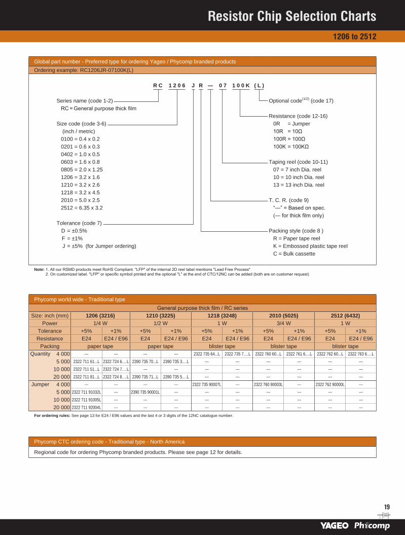
Global part number - Preferred type for ordering Yageo / Phycomp branded productsOrdering example: RC1206JR-07100K(L)
R C 1 2 0 6 J R ― 0 7 1 0 0 K ( L )
Series name (code 1-2) Optional code(1/2) (code 17) RC = General purpose thick film
Resistance (code 12-16)Size code (code 3-6) 0R = Jumper
(inch / metric) 10R = 10Ω0100 = 0.4 x 0.2 100R = 100Ω0201 = 0.6 x 0.3 100K = 100KΩ0402 = 1.0 x 0.50603 = 1.6 x 0.8 Taping reel (code 10-11)0805 = 2.0 x 1.25 07 = 7 inch Dia. reel1206 = 3.2 x 1.6 10 = 10 inch Dia. reel1210 = 3.2 x 2.6 13 = 13 inch Dia. reel1218 = 3.2 x 4.52010 = 5.0 x 2.5 T. C. R. (code 9)2512 = 6.35 x 3.2 “―” = Based on spec.
(― for thick film only)Tolerance (code 7)
D = ±0.5% Packing style (code 8 ) F = ±1% R = Paper tape reel J = ±5% (for Jumper ordering) K = Embossed plastic tape reel
C = Bulk cassette
Note: 1. All our RSMD products meet RoHS Compliant. "LFP" of the internal 2D reel label mentions "Lead Free Process" 2. On customized label. "LFP" or specific symbol printed and the optional "L" at the end of CTC/12NC can be added (both are on customer request)
Phycomp world wide - Traditional typeGeneral purpose thick film / RC series
Size: inch (mm) 1206 (3216) 1210 (3225) 1218 (3248) 2010 (5025) 2512 (6432)Power 1/4 W 1/2 W 1 W 3/4 W 1 W
Tolerance +5% +1% +5% +1% +5% +1% +5% +1% +5% +1%Resistance E24 E24 / E96 E24 E24 / E96 E24 E24 / E96 E24 E24 / E96 E24 E24 / E96
Packing paper tape paper tape blister tape blister tape blister tapeQuantity 4 000 --- --- --- --- 2322 735 64...L 2322 735 7.…L 2322 760 60...L 2322 761 6.…L 2322 762 60...L 2322 763 6.…L
5 000 2322 711 61...L 2322 724 6.…L 2390 735 70...L 2390 735 3.…L --- --- --- --- --- ---
10 000 2322 711 51...L 2322 724 7.…L --- --- --- --- --- --- --- ---
20 000 2322 711 81...L 2322 724 8.…L 2390 735 71...L 2390 735 5.…L --- --- --- --- --- ---Jumper 4 000 --- --- --- --- 2322 735 90007L --- 2322 760 90003L --- 2322 762 90000L ---
5 000 2322 711 91032L --- 2390 735 90001L --- --- --- --- --- --- ---
10 000 2322 711 91005L --- --- --- --- --- --- --- --- ---
20 000 2322 711 92004L --- --- --- --- --- --- --- --- ---
For ordering rules: See page 13 for E24 / E96 values and the last 4 or 3 digits of the 12NC catalogue number.
Phycomp CTC ordering code - Traditional type - North America
Regional code for ordering Phycomp branded products. Please see page 12 for details.
Resistor Chip Selection Charts1206 to 2512
20
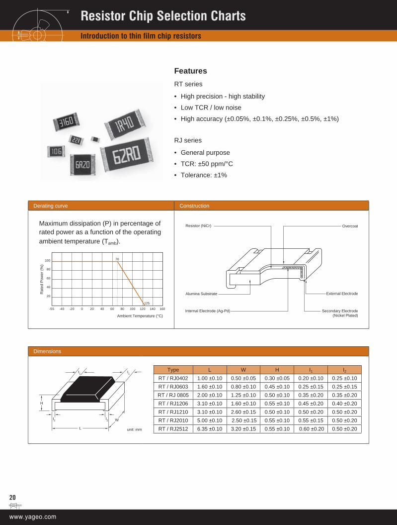
Derating curve Construction
Maximum dissipation (P) in percentage of rated power as a function of the operating ambient temperature (Tamb).
100
80
60
40
20
-55 -40 -20 0 20 40 60 80
70
100 120 140 160
Ambient Temperature (°C)
Ra
ted
Po
we
r (%
)
125
Overcoat
Secondary Electrode (Nickel Plated)
External Electrode
Resistor (NiCr)
Alumina Substrate
Internal Electrode (Ag-Pd)
Dimensions
W
unit: mm
I2
I2
I1
I1
L
H
Type L W H I1 I2
RT / RJ0402 1.00 ±0.10 0.50 ±0.05 0.30 ±0.05 0.20 ±0.10 0.25 ±0.10RT / RJ0603 1.60 ±0.10 0.80 ±0.10 0.45 ±0.10 0.25 ±0.15 0.25 ±0.15RT / RJ 0805 2.00 ±0.10 1.25 ±0.10 0.50 ±0.10 0.35 ±0.20 0.35 ±0.20RT / RJ1206 3.10 ±0.10 1.60 ±0.10 0.55 ±0.10 0.45 ±0.20 0.40 ±0.20RT / RJ1210 3.10 ±0.10 2.60 ±0.15 0.50 ±0.10 0.50 ±0.20 0.50 ±0.20RT / RJ2010 5.00 ±0.10 2.50 ±0.15 0.55 ±0.10 0.55 ±0.15 0.50 ±0.20RT / RJ2512 6.35 ±0.10 3.20 ±0.15 0.55 ±0.10 0.60 ±0.20 0.50 ±0.20
Features
RT series
High precision - high stability
Low TCR / low noise
High accuracy (±0.05%, ±0.1%, ±0.25%, ±0.5%, ±1%)
RJ series
General purpose
TCR: ±50 ppm/°C
Tolerance: ±1%
•
•
•
•
•
•
Resistor Chip Selection ChartsIntroduction to thin film chip resistors
21
Electrical characteristics
Type Power P70
Operating Temp. range MWV RCOV DWV Resistance range & tolerance T. C. R.
( ppm/°C)
RT0402 1/16W
-55°C to +125°C
50V 100V 75V
E24/E96 ±0.05%, ±0.1%,
±0.25%, ±0.5%, ±1%
10Ω ≤ R ≤ 121KΩ
±50±25±15±10
RT0603 1/10W 75V 150V 100V 10Ω ≤ R ≤ 681KΩRT0805 1/8W 150V 300V 200V
10Ω ≤ R ≤ 1.5MΩRT1206 1/8W 200V 400V 300VRT1210 1/4W 200V 400V 400V 10Ω ≤ R ≤ 1MΩRT2010 1/2W 200V 400V 400V
10Ω ≤ R ≤ 1MΩRT2512 3/4W 200V 400V 400VRJ0402 1/16W 25V 100V 100V
E24/E96 ±1%
10Ω ≤ R ≤ 121KΩ
±50
RJ0603 1/16W 50V 100V 100V 5.1Ω ≤ R ≤ 681KΩRJ0805 1/10W 100V 200V 250V
5.1Ω ≤ R ≤ 1.5MΩRJ1206 1/8W 150V 250V 250VRJ1210 1/4W 150V 250V 250V
10Ω ≤ R ≤ 1MΩRJ2010 1/2W 150V 300V 400VRJ2512 3/4W 150V 300V 400V
Environmental characteristics
Performance test Test method Procedure Requirements
Life MIL-STD-202G-method 108A
1 000 hours at 70 ±5°C applied RCWV 1.5 hours on, 0.5 hours off, still air required
±(0.25% +0.05Ω) for RT ±(0.5% +0.05Ω) for RJ
High temperature exposure MIL-STD-202G-method 108A
1 000 hours at maximum operating temperature depending on specification, unpowered
Moisture resistance MIL-STD-202G-method 106F
Each temperature / humidity cycle is defined at 8 hours (method 106F), 3 cycles / 24 hours for 10d with 25°C / 65°C 95% R.H
Thermal shock MIL-STD-202G-method 107G
LCT / UCT, number of cycles required is 300 Maximum transfer time is 20 seconds
Short time overload MIL-R-55342D-para 4.7.5
2.5 times RCWV or maximum overload voltage which-ever is less for 5 seconds at room temperature
Solderability
Resistance to soldering heat
MIL-STD-202G-method 210F Leadfree solder, 270°C, 10 seconds immersion time ±(0.25% +0.05Ω) for RT
±(0.5% +0.05Ω) for RJ
Wetting IPC/JEDECJ-STD-002B testB
Electrical test not required. Magnification 50X Leadfree solder bath at 245 ±3°C Dipping time: 3 ±0.5 seconds
Well tinned (≥95% covered)
Resistor Chip Selection ChartsIntroduction to thin film chip resistors

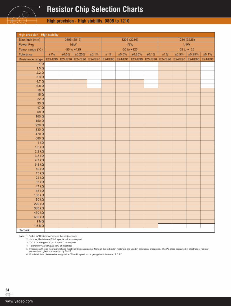
22
High precision - High stabilitySize: inch (mm) 0402 (1005) 0603 (1608)Power P70 1/16W 1/10WTemp. range (°C) -55 to +125 -55 to +125Tolerance ±1% ±0.5% ±0.25% ±0.1% ±1% ±0.5% ±0.25% ±0.1%Resistance range E24/E96 E24/E96 E24/E96 E24/E96 E24/E96 E24/E96 E24/E96 E24/E96
1 Ω1.5 Ω2.2 Ω3.3 Ω4.7 Ω6.8 Ω10 Ω15 Ω22 Ω33 Ω47 Ω68 Ω
100 Ω150 Ω220 Ω330 Ω470 Ω680 Ω
1 kΩ1.5 kΩ2.2 kΩ3.3 kΩ4.7 kΩ6.8 kΩ10 kΩ15 kΩ22 kΩ33 kΩ47 kΩ68 kΩ
100 kΩ150 kΩ220 kΩ330 kΩ470 kΩ680 kΩ
Remark
Note: 1. Resistance range is upper to 2 MΩ (depends on size) on request2. Value in "Resistance" means the minimum one3. Resistance E192; special value on request4. Tolerance = ±0.05%, T.C.R. = ±10 ppm/°C; ±15 ppm/°C on request5. Products with lead free terminations meet RoHS requirements. None of the forbidden materials are used in products / production. The Pb-glass contained in electrodes, resistor
element and glass is exempted by RoHS.6. For detail data please refer to right side "Thin film product range against tolerance / T.C.R."
Resistor Chip Selection ChartsHigh precision - High stability, 0402 / 0603

23
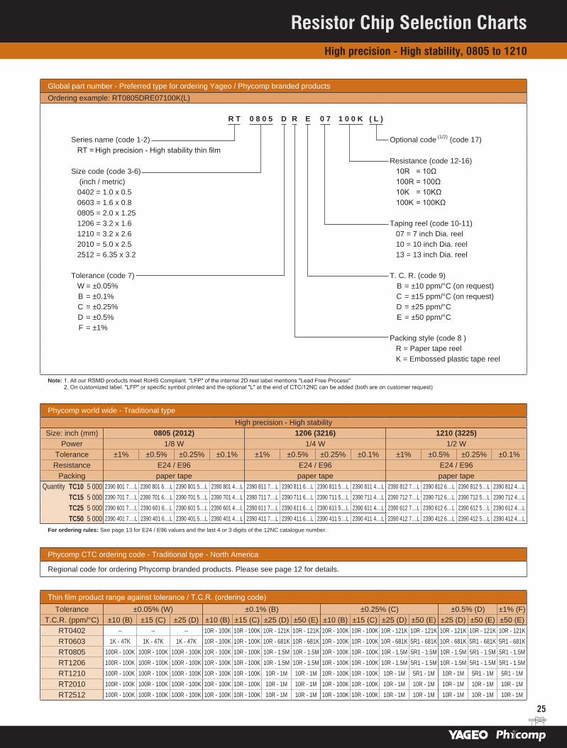
Global part number - Preferred type for ordering Yageo / Phycomp branded productsOrdering example: RT0603DRE07100K(L)
R T 0 6 0 3 D R E 0 7 1 0 0 K ( L )
Series name (code 1-2) Optional code (1/2) (code 17) RT = High precision - High stability thin film
Resistance (code 12-16)Size code (code 3-6) 10R = 10Ω
(inch / metric) 100R = 100Ω0402 = 1.0 x 0.5 10K = 10KΩ0603 = 1.6 x 0.8 100K = 100KΩ0805 = 2.0 x 1.251206 = 3.2 x 1.6 Taping reel (code 10-11)1210 = 3.2 x 2.6 07 = 7 inch Dia. reel2010 = 5.0 x 2.5 10 = 10 inch Dia. reel2512 = 6.35 x 3.2 13 = 13 inch Dia. reel
Tolerance (code 7) T. C. R. (code 9) W = ±0.05% B = ±10 ppm/°C (on request) B = ±0.1% C = ±15 ppm/°C (on request) C = ±0.25% D = ±25 ppm/°C D = ±0.5% E = ±50 ppm/°C F = ±1%
Packing style (code 8 )R = Paper tape reelK = Embossed plastic tape reel
Note: 1. All our RSMD products meet RoHS Compliant. "LFP" of the internal 2D reel label mentions "Lead Free Process" 2. On customized label. "LFP" or specific symbol printed and the optional "L" at the end of CTC/12NC can be added (both are on customer request)
Phycomp world wide - Traditional typeHigh precision - High stability
Size: inch (mm) 0402 (1005) 0603 (1608)Power 1/16 W 1/10 W
Tolerance ±1% ±0.5% ±0.25% ±0.1% ±1% ±0.5% ±0.25% ±0.1%Resistance E24 / E96 E24 / E96
Packing paper tape paper tapeQuantity TC25 5 000 --- --- --- --- 2390 604 7.…L 2390 604 6.…L 2390 604 5.…L 2390 604 4.…L
TC50 5 000 --- --- --- --- 2390 404 7.…L 2390 404 6.…L 2390 404 5.…L 2390 404 4.…L
TC25 10 000 2390 607 7.…L 2390 607 6.…L 2390 607 5.…L 2390 607 4.…L --- --- --- ---
TC50 10 000 2390 407 7.…L 2390 407 6.…L 2390 407 5.…L 2390 407 4.…L --- --- --- ---
For ordering rules: See page 13 for E24 / E96 values and the last 4 or 3 digits of the 12NC catalogue number.
Phycomp CTC ordering code - Traditional type - North America
Regional code for ordering Phycomp branded products. Please see page 12 for details.
Thin film product range against tolerance / T.C.R. (ordering code)Tolerance ±0.05% (W) ±0.1% (B) ±0.25% (C) ±0.5% (D) ±1% (F)
T.C.R. (ppm/°C) ±10 (B) ±15 (C) ±25 (D) ±10 (B) ±15 (C) ±25 (D) ±50 (E) ±10 (B) ±15 (C) ±25 (D) ±50 (E) ±25 (D) ±50 (E) ±50 (E)RT0402 -- -- -- 10R - 100K 10R - 100K 10R - 121K 10R - 121K 10R - 100K 10R - 100K 10R - 121K 10R - 121K 10R - 121K 10R - 121K 10R - 121K
RT0603 1K - 47K 1K - 47K 1K - 47K 10R - 100K 10R - 100K 10R - 681K 10R - 681K 10R - 100K 10R - 100K 10R - 681K 5R1 - 681K 10R - 681K 5R1 - 681K 5R1 - 681K
RT0805 100R - 100K 100R - 100K 100R - 100K 10R - 100K 10R - 100K 10R - 1.5M 10R - 1.5M 10R - 100K 10R - 100K 10R - 1.5M 5R1 - 1.5M 10R - 1.5M 5R1 - 1.5M 5R1 - 1.5M
RT1206 100R - 100K 100R - 100K 100R - 100K 10R - 100K 10R - 100K 10R - 1.5M 10R - 1.5M 10R - 100K 10R - 100K 10R - 1.5M 5R1 - 1.5M 10R - 1.5M 5R1 - 1.5M 5R1 - 1.5M
RT1210 100R - 100K 100R - 100K 100R - 100K 10R - 100K 10R - 100K 10R - 1M 10R - 1M 10R - 100K 10R - 100K 10R - 1M 5R1 - 1M 10R - 1M 5R1 - 1M 5R1 - 1M
RT2010 100R - 100K 100R - 100K 100R - 100K 10R - 100K 10R - 100K 10R - 1M 10R - 1M 10R - 100K 10R - 100K 10R - 1M 10R - 1M 10R - 1M 10R - 1M 10R - 1M
RT2512 100R - 100K 100R - 100K 100R - 100K 10R - 100K 10R - 100K 10R - 1M 10R - 1M 10R - 100K 10R - 100K 10R - 1M 10R - 1M 10R - 1M 10R - 1M 10R - 1M
Resistor Chip Selection ChartsHigh precision - High stability, 0402 / 0603
24
High precision - High stabilitySize: inch (mm) 0805 (2012) 1206 (3216) 1210 (3225)Power P70 1/8W 1/8W 1/4WTemp. range (°C) -55 to +125 -55 to +125 -55 to +125Tolerance ±1% ±0.5% ±0.25% ±0.1% ±1% ±0.5% ±0.25% ±0.1% ±1% ±0.5% ±0.25% ±0.1%Resistance range E24/E96 E24/E96 E24/E96 E24/E96 E24/E96 E24/E96 E24/E96 E24/E96 E24/E96 E24/E96 E24/E96 E24/E96
1 Ω1.5 Ω2.2 Ω3.3 Ω4.7 Ω6.8 Ω10 Ω15 Ω22 Ω33 Ω47 Ω68 Ω
100 Ω150 Ω220 Ω330 Ω470 Ω680 Ω
1 kΩ1.5 kΩ2.2 kΩ3.3 kΩ4.7 kΩ6.8 kΩ10 kΩ15 kΩ22 kΩ33 kΩ47 kΩ68 kΩ
100 kΩ150 kΩ220 kΩ330 kΩ470 kΩ680 kΩ
1 MΩ1.5 MΩ
Remark
Note: 1. Value in "Resistance" means the minimum one2. Jumper; Resistance E192; special value on request3. T.C.R. = ±10 ppm/°C; ±15 ppm/°C on request4. Tolerance = ±0.01%; ±0.05% on Request5. Products with lead free terminations meet RoHS requirements. None of the forbidden materials are used in products / production. The Pb-glass contained in electrodes, resistor
element and glass is exempted by RoHS.6. For detail data please refer to right side "Thin film product range against tolerance / T.C.R."
Resistor Chip Selection ChartsHigh precision - High stability, 0805 to 1210
25
Global part number - Preferred type for ordering Yageo / Phycomp branded productsOrdering example: RT0805DRE07100K(L)
R T 0 8 0 5 D R E 0 7 1 0 0 K ( L )
Series name (code 1-2) Optional code (1/2) (code 17) RT = High precision - High stability thin film
Resistance (code 12-16)Size code (code 3-6) 10R = 10Ω
(inch / metric) 100R = 100Ω0402 = 1.0 x 0.5 10K = 10KΩ0603 = 1.6 x 0.8 100K = 100KΩ0805 = 2.0 x 1.251206 = 3.2 x 1.6 Taping reel (code 10-11)1210 = 3.2 x 2.6 07 = 7 inch Dia. reel2010 = 5.0 x 2.5 10 = 10 inch Dia. reel2512 = 6.35 x 3.2 13 = 13 inch Dia. reel
Tolerance (code 7) T. C. R. (code 9) W = ±0.05% B = ±10 ppm/°C (on request) B = ±0.1% C = ±15 ppm/°C (on request) C = ±0.25% D = ±25 ppm/°C D = ±0.5% E = ±50 ppm/°C F = ±1%
Packing style (code 8 )R = Paper tape reelK = Embossed plastic tape reel
Note: 1. All our RSMD products meet RoHS Compliant. "LFP" of the internal 2D reel label mentions "Lead Free Process" 2. On customized label. "LFP" or specific symbol printed and the optional "L" at the end of CTC/12NC can be added (both are on customer request)
Phycomp world wide - Traditional typeHigh precision - High stability
Size: inch (mm) 0805 (2012) 1206 (3216) 1210 (3225)Power 1/8 W 1/4 W 1/2 W
Tolerance ±1% ±0.5% ±0.25% ±0.1% ±1% ±0.5% ±0.25% ±0.1% ±1% ±0.5% ±0.25% ±0.1%Resistance E24 / E96 E24 / E96 E24 / E96
Packing paper tape paper tape paper tapeQuantity TC10 5 000 2390 801 7.…L 2390 801 6.…L 2390 801 5....L 2390 801 4....L 2390 811 7....L 2390 811 6....L 2390 811 5....L 2390 811 4....L 2390 812 7....L 2390 812 6....L 2390 812 5....L 2390 812 4....L
TC15 5 000 2390 701 7.…L 2390 701 6.…L 2390 701 5....L 2390 701 4....L 2390 711 7....L 2390 711 6....L 2390 711 5....L 2390 711 4....L 2390 712 7....L 2390 712 6....L 2390 712 5....L 2390 712 4....L
TC25 5 000 2390 601 7.…L 2390 601 6....L 2390 601 5....L 2390 601 4....L 2390 611 7....L 2390 611 6....L 2390 611 5....L 2390 611 4....L 2390 612 7....L 2390 612 6....L 2390 612 5....L 2390 612 4....L
TC50 5 000 2390 401 7.…L 2390 401 6....L 2390 401 5....L 2390 401 4....L 2390 411 7....L 2390 411 6....L 2390 411 5....L 2390 411 4....L 2390 412 7....L 2390 412 6....L 2390 412 5....L 2390 412 4....L
For ordering rules: See page 13 for E24 / E96 values and the last 4 or 3 digits of the 12NC catalogue number.
Phycomp CTC ordering code - Traditional type - North America
Regional code for ordering Phycomp branded products. Please see page 12 for details.
Thin film product range against tolerance / T.C.R. (ordering code)Tolerance ±0.05% (W) ±0.1% (B) ±0.25% (C) ±0.5% (D) ±1% (F)
T.C.R. (ppm/°C) ±10 (B) ±15 (C) ±25 (D) ±10 (B) ±15 (C) ±25 (D) ±50 (E) ±10 (B) ±15 (C) ±25 (D) ±50 (E) ±25 (D) ±50 (E) ±50 (E)RT0402 -- -- -- 10R - 100K 10R - 100K 10R - 121K 10R - 121K 10R - 100K 10R - 100K 10R - 121K 10R - 121K 10R - 121K 10R - 121K 10R - 121K
RT0603 1K - 47K 1K - 47K 1K - 47K 10R - 100K 10R - 100K 10R - 681K 10R - 681K 10R - 100K 10R - 100K 10R - 681K 5R1 - 681K 10R - 681K 5R1 - 681K 5R1 - 681K
RT0805 100R - 100K 100R - 100K 100R - 100K 10R - 100K 10R - 100K 10R - 1.5M 10R - 1.5M 10R - 100K 10R - 100K 10R - 1.5M 5R1 - 1.5M 10R - 1.5M 5R1 - 1.5M 5R1 - 1.5M
RT1206 100R - 100K 100R - 100K 100R - 100K 10R - 100K 10R - 100K 10R - 1.5M 10R - 1.5M 10R - 100K 10R - 100K 10R - 1.5M 5R1 - 1.5M 10R - 1.5M 5R1 - 1.5M 5R1 - 1.5M
RT1210 100R - 100K 100R - 100K 100R - 100K 10R - 100K 10R - 100K 10R - 1M 10R - 1M 10R - 100K 10R - 100K 10R - 1M 5R1 - 1M 10R - 1M 5R1 - 1M 5R1 - 1M
RT2010 100R - 100K 100R - 100K 100R - 100K 10R - 100K 10R - 100K 10R - 1M 10R - 1M 10R - 100K 10R - 100K 10R - 1M 10R - 1M 10R - 1M 10R - 1M 10R - 1M
RT2512 100R - 100K 100R - 100K 100R - 100K 10R - 100K 10R - 100K 10R - 1M 10R - 1M 10R - 100K 10R - 100K 10R - 1M 10R - 1M 10R - 1M 10R - 1M 10R - 1M
Resistor Chip Selection ChartsHigh precision - High stability, 0805 to 1210
26
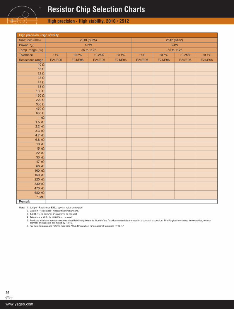
High precision - high stabilitySize: inch (mm) 2010 (5025) 2512 (6432)Power P70 1/2W 3/4WTemp. range (°C) -55 to +125 -55 to +125Tolerance ±1% ±0.5% ±0.25% ±0.1% ±1% ±0.5% ±0.25% ±0.1%Resistance range E24/E96 E24/E96 E24/E96 E24/E96 E24/E96 E24/E96 E24/E96 E24/E96
10 Ω15 Ω22 Ω33 Ω47 Ω68 Ω
100 Ω150 Ω220 Ω330 Ω470 Ω680 Ω
1 kΩ1.5 kΩ2.2 kΩ3.3 kΩ4.7 kΩ6.8 kΩ10 kΩ15 kΩ22 kΩ33 kΩ47 kΩ68 kΩ
100 kΩ150 kΩ220 kΩ330 kΩ470 kΩ680 kΩ
1 MΩRemark
Note: 1. Jumper; Resistance E192; special value on request2. Value in "Resistance" means the minimum one.3. T.C.R. = ±10 ppm/°C; ±15 ppm/°C on request4. Tolerance = ±0.01%; ±0.05% on request5. Products with lead free terminations meet RoHS requirements. None of the forbidden materials are used in products / production. The Pb-glass contained in electrodes, resistor
element and glass is exempted by RoHS.6. For detail data please refer to right side "Thin film product range against tolerance / T.C.R."
Resistor Chip Selection ChartsHigh precision - High stability, 2010 / 2512
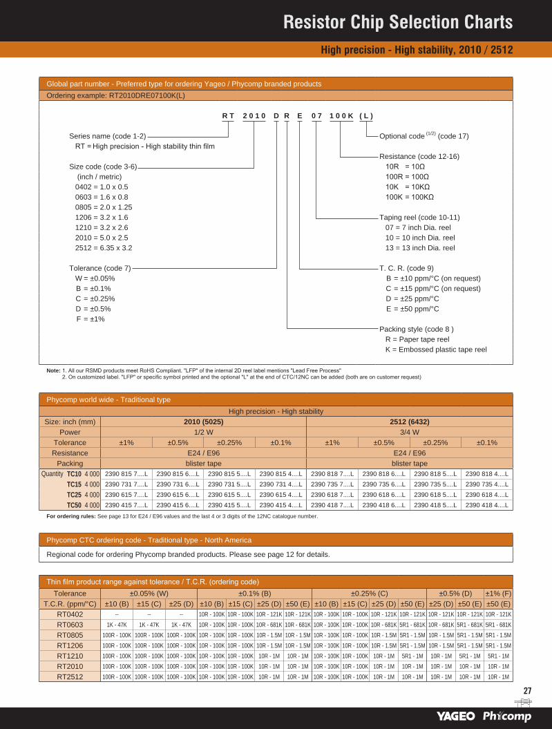
27
Global part number - Preferred type for ordering Yageo / Phycomp branded productsOrdering example: RT2010DRE07100K(L)
R T 2 0 1 0 D R E 0 7 1 0 0 K ( L )
Series name (code 1-2) Optional code (1/2) (code 17) RT = High precision - High stability thin film
Resistance (code 12-16)Size code (code 3-6) 10R = 10Ω
(inch / metric) 100R = 100Ω0402 = 1.0 x 0.5 10K = 10KΩ0603 = 1.6 x 0.8 100K = 100KΩ0805 = 2.0 x 1.251206 = 3.2 x 1.6 Taping reel (code 10-11)1210 = 3.2 x 2.6 07 = 7 inch Dia. reel2010 = 5.0 x 2.5 10 = 10 inch Dia. reel2512 = 6.35 x 3.2 13 = 13 inch Dia. reel
Tolerance (code 7) T. C. R. (code 9) W = ±0.05% B = ±10 ppm/°C (on request) B = ±0.1% C = ±15 ppm/°C (on request) C = ±0.25% D = ±25 ppm/°C D = ±0.5% E = ±50 ppm/°C F = ±1%
Packing style (code 8 )R = Paper tape reelK = Embossed plastic tape reel
Note: 1. All our RSMD products meet RoHS Compliant. "LFP" of the internal 2D reel label mentions "Lead Free Process" 2. On customized label. "LFP" or specific symbol printed and the optional "L" at the end of CTC/12NC can be added (both are on customer request)
Phycomp world wide - Traditional typeHigh precision - High stability
Size: inch (mm) 2010 (5025) 2512 (6432)Power 1/2 W 3/4 W
Tolerance ±1% ±0.5% ±0.25% ±0.1% ±1% ±0.5% ±0.25% ±0.1%Resistance E24 / E96 E24 / E96
Packing blister tape blister tapeQuantity TC10 4 000 2390 815 7....L 2390 815 6....L 2390 815 5....L 2390 815 4....L 2390 818 7....L 2390 818 6....L 2390 818 5....L 2390 818 4....L
TC15 4 000 2390 731 7....L 2390 731 6....L 2390 731 5....L 2390 731 4....L 2390 735 7....L 2390 735 6....L 2390 735 5....L 2390 735 4....L
TC25 4 000 2390 615 7....L 2390 615 6....L 2390 615 5....L 2390 615 4....L 2390 618 7....L 2390 618 6....L 2390 618 5....L 2390 618 4....L
TC50 4 000 2390 415 7....L 2390 415 6....L 2390 415 5....L 2390 415 4....L 2390 418 7....L 2390 418 6....L 2390 418 5....L 2390 418 4....L
For ordering rules: See page 13 for E24 / E96 values and the last 4 or 3 digits of the 12NC catalogue number.
Phycomp CTC ordering code - Traditional type - North America
Regional code for ordering Phycomp branded products. Please see page 12 for details.
Thin film product range against tolerance / T.C.R. (ordering code)Tolerance ±0.05% (W) ±0.1% (B) ±0.25% (C) ±0.5% (D) ±1% (F)
T.C.R. (ppm/°C) ±10 (B) ±15 (C) ±25 (D) ±10 (B) ±15 (C) ±25 (D) ±50 (E) ±10 (B) ±15 (C) ±25 (D) ±50 (E) ±25 (D) ±50 (E) ±50 (E)RT0402 -- -- -- 10R - 100K 10R - 100K 10R - 121K 10R - 121K 10R - 100K 10R - 100K 10R - 121K 10R - 121K 10R - 121K 10R - 121K 10R - 121K
RT0603 1K - 47K 1K - 47K 1K - 47K 10R - 100K 10R - 100K 10R - 681K 10R - 681K 10R - 100K 10R - 100K 10R - 681K 5R1 - 681K 10R - 681K 5R1 - 681K 5R1 - 681K
RT0805 100R - 100K 100R - 100K 100R - 100K 10R - 100K 10R - 100K 10R - 1.5M 10R - 1.5M 10R - 100K 10R - 100K 10R - 1.5M 5R1 - 1.5M 10R - 1.5M 5R1 - 1.5M 5R1 - 1.5M
RT1206 100R - 100K 100R - 100K 100R - 100K 10R - 100K 10R - 100K 10R - 1.5M 10R - 1.5M 10R - 100K 10R - 100K 10R - 1.5M 5R1 - 1.5M 10R - 1.5M 5R1 - 1.5M 5R1 - 1.5M
RT1210 100R - 100K 100R - 100K 100R - 100K 10R - 100K 10R - 100K 10R - 1M 10R - 1M 10R - 100K 10R - 100K 10R - 1M 5R1 - 1M 10R - 1M 5R1 - 1M 5R1 - 1M
RT2010 100R - 100K 100R - 100K 100R - 100K 10R - 100K 10R - 100K 10R - 1M 10R - 1M 10R - 100K 10R - 100K 10R - 1M 10R - 1M 10R - 1M 10R - 1M 10R - 1M
RT2512 100R - 100K 100R - 100K 100R - 100K 10R - 100K 10R - 100K 10R - 1M 10R - 1M 10R - 100K 10R - 100K 10R - 1M 10R - 1M 10R - 1M 10R - 1M 10R - 1M
Resistor Chip Selection ChartsHigh precision - High stability, 2010 / 2512
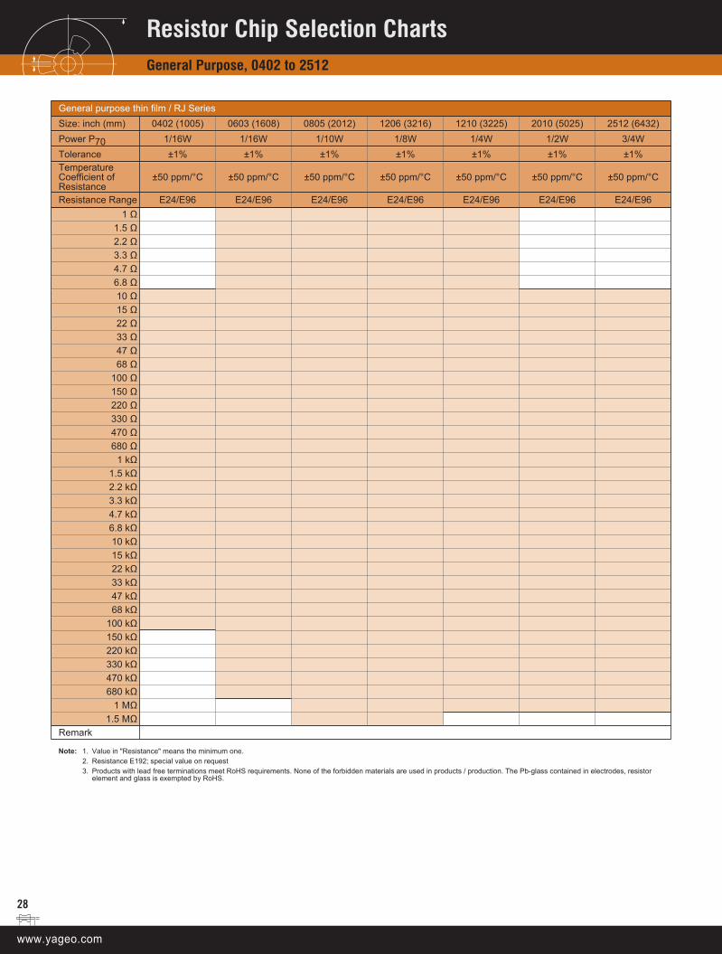
28
General purpose thin film / RJ SeriesSize: inch (mm) 0402 (1005) 0603 (1608) 0805 (2012) 1206 (3216) 1210 (3225) 2010 (5025) 2512 (6432)Power P70 1/16W 1/16W 1/10W 1/8W 1/4W 1/2W 3/4WTolerance ±1% ±1% ±1% ±1% ±1% ±1% ±1%TemperatureCoefficient ofResistance
±50 ppm/°C ±50 ppm/°C ±50 ppm/°C ±50 ppm/°C ±50 ppm/°C ±50 ppm/°C ±50 ppm/°C
Resistance Range E24/E96 E24/E96 E24/E96 E24/E96 E24/E96 E24/E96 E24/E961 Ω
1.5 Ω2.2 Ω3.3 Ω4.7 Ω6.8 Ω10 Ω15 Ω22 Ω33 Ω47 Ω68 Ω
100 Ω150 Ω220 Ω330 Ω470 Ω680 Ω
1 kΩ1.5 kΩ2.2 kΩ3.3 kΩ4.7 kΩ6.8 kΩ10 kΩ15 kΩ22 kΩ33 kΩ47 kΩ68 kΩ
100 kΩ150 kΩ220 kΩ330 kΩ470 kΩ680 kΩ
1 MΩ1.5 MΩ
Remark
Note: 1. Value in "Resistance" means the minimum one.2. Resistance E192; special value on request3. Products with lead free terminations meet RoHS requirements. None of the forbidden materials are used in products / production. The Pb-glass contained in electrodes, resistor
element and glass is exempted by RoHS.
Resistor Chip Selection ChartsGeneral Purpose, 0402 to 2512
29
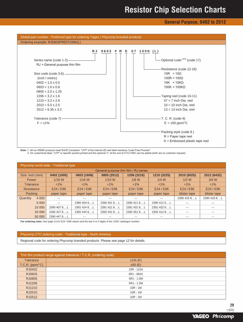
Global part number - Preferred type for ordering Yageo / Phycomp branded productsOrdering example: RJ0603FRE07100K(L)
R J 0 6 0 3 F R E 0 7 1 0 0 K ( L )
Series name (code 1-2) Optional code (1/2) (code 17) RJ = General purpose thin film
Resistance (code 12-16)Size code (code 3-6) 10R = 10Ω
(inch / metric) 100R = 100Ω0402 = 1.0 x 0.5 10K = 10KΩ0603 = 1.6 x 0.8 100K = 100KΩ0805 = 2.0 x 1.251206 = 3.2 x 1.6 Taping reel (code 10-11)1210 = 3.2 x 2.6 07 = 7 inch Dia. reel2010 = 5.0 x 2.5 10 = 10 inch Dia. reel2512 = 6.35 x 3.2 13 = 13 inch Dia. reel
Tolerance (code 7) T. C. R. (code 9) F = ±1% E = ±50 ppm/°C
Packing style (code 8 )R = Paper tape reelK = Embossed plastic tape reel
Note: 1. All our RSMD products meet RoHS Compliant. "LFP" of the internal 2D reel label mentions "Lead Free Process" 2. On customized label. "LFP" or specific symbol printed and the optional "L" at the end of CTC/12NC can be added (both are on customer request)
Phycomp world wide - Traditional typeGeneral purpose thin film / RJ series
Size: inch (mm) 0402 (1005) 0603 (1608) 0805 (2012) 1206 (3216) 1210 (3225) 2010 (5025) 2512 (6432)Power 1/16 W 1/16 W 1/10 W 1/8 W 1/4 W 1/2 W 3/4 W
Tolerance +1% +1% +1% +1% +1% +1% +1%Resistance E24 / E96 E24 / E96 E24 / E96 E24 / E96 E24 / E96 E24 / E96 E24 / E96
Packing paper tape paper tape paper tape paper tape paper tape blister tape blister tapeQuantity 4 000 --- --- --- --- --- 2390 415 8.…L 2390 418 8.…L
5 000 --- 2390 404 8.…L 2390 401 8.…L 2390 411 8.…L 2390 412 0.…L --- ---
10 000 2390 407 8.…L 2391 424 8.…L 2391 421 8.…L 2391 431 8.…L 2391 432 8.…L --- ---
20 000 2390 427 8.…L 2392 444 8.…L 2392 441 8.…L 2392 451 8.…L 2392 412 8.…L --- ---
50 000 2390 447 8.…L --- --- --- --- --- ---
For ordering rules: See page 13 for E24 / E96 values and the last 4 or 3 digits of the 12NC catalogue number.
Phycomp CTC ordering code - Traditional type - North America
Regional code for ordering Phycomp branded products. Please see page 12 for details.
Thin film product range against tolerance / T.C.R. (ordering code)Tolerance ±1% (F)
T.C.R. (ppm/°C) ±50 (E)RJ0402 10R - 121K
RJ0603 5R1 - 681K
RJ0805 5R1 - 1.5M
RJ1206 5R1 - 1.5M
RJ1210 10R - 1M
RJ2010 10R - 1M
RJ2512 10R - 1M
Resistor Chip Selection ChartsGeneral Purpose, 0402 to 2512

30
FeaturesIntegrated discrete chip resistors from 2 to 8 pcs
More efficient in pick & place application
Low assembly costs
Reduced size of final equipment
Higher component and equipment reliability
•
•
•
•
•
Schematics
TC122
R1 = R2
R1 = R2
YC102/122/162
4 3
1 2
R2R1
4 3
R2R1
1 2
TC124/164
R1 = R2 = R3 = R4
YC124/164/324
R1 = R2 = R3 = R4
5 6 7 8
1 2 3 4
R1 R2 R3 R4
YC158
R1 = R2 = R3 = R4 = R5 = R6 = R7 = R8
R1 = R2 = R3 = R4 = R5 = R6 = R7 = R8
YC248
R1 R2 R3 R4 R5 R6 R7 R8
1 2 3 4 5 6 7 8
16 15 14 13 12 11 10 9
1 2 3 4 5
10 9 8 7 6
R1 R2 R3 R4
R8 R7 R6 R5
R1 = R2 = R3 = R4 = R5 = R6 = R7 = R8
R1 = R2 = R3 = R4 = R5 = R6 = R7 = R8
YC358 (L-Type)
YC358 (T-Type)
R1 R2 R3 R4
R8 R7 R6 R5
1 2 3 4 5
10 9 8 7 6
1 2 3 4 5
10 9 8 7 6
R1 R2 R3 R4
R8 R7 R6 R5
5 6 7 8
1 2 3 4
R1 R2 R3 R4
Dimensions
Side view for all types
T
W1
W2
YC 102/122/162
H
B
P
L
YC 124/164/324 158/358/248
H
L
B
H2
a
a
P
L
TC 122
P
L
B
H
TC 124/164
B
Ha
a
P
H2
Note: "H2" is valued on button view unit: mm
Type H / H2 B P L T W1 W2
YC102 H: 0.35 ±0.10 0.20 ±0.10 0.50 ±0.05 0.80 ±0.10 0.35 ±0.10 0.15 ±0.10 0.60 ±0.10YC122 H: 0.21 +0.10/-0.05 0.20 ±0.10 0.67 ±0.05 1.00 ±0.10 0.35 ±0.10 0.25 ±0.10 1.00 ±0.10YC162 H: 0.30 ±0.10 0.30 ±0.10 0.80 ±0.05 1.60 ±0.10 0.40 ±0.10 0.30 ±0.10 1.60 ±0.10YC124 H: 0.45 ±0.05 0.20 ±0.15 0.50 ±0.05 2.00 ±0.10 0.45 ±0.10 0.30 ±0.15 1.00 ±0.10YC164 H: 0.65 ±0.05 0.30 ±0.15 0.80 ±0.05 3.20 ±0.15 0.60 ±0.10 0.30 ±0.15 1.60 ±0.15
YC324 H: 1.10 ±0.15 H2: 0.90 ±0.15 0.50 ±0.20 1.27 ±0.05 5.08 ±0.20 0.60 ±0.10 0.50 ±0.15 3.20 ±0.20
YC248 H: 0.45 ±0.05 H2: 0.30 ±0.05 0.30 ±0.15 0.50 ±0.05 4.00 ±0.20 0.45 ±0.10 0.40 ±0.15 1.60 ±0.15
TC122 H: 0.30 ±0.05 0.25 ±0.15 0.50 ±0.05 1.00 ±0.10 0.30 ±0.10 0.25 ±0.15 1.00 ±0.10
TC124 H: 0.30 ±0.10 H2: 0.25 ±0.10 0.20 ±0.10 0.50 ±0.05 2.00 ±0.10 0.40 ±0.10 0.25 ±0.10 1.00 ±0.10
TC164 H: ---H2: 0.60 ±0.15 0.30 ±0.15 0.80 ±0.05 3.20 ±0.15 0.60 ±0.10 0.30 ±0.15 1.60 ±0.15
YC158 H: 0.45 ±0.05 0.30 ±0.15 0.64 ±0.05 3.20 ±0.20 0.60 ±0.10 0.35 ±0.15 1.60 ±0.15
YC358 H: 1.10 ±0.15 H2: 0.90 ±0.15 0.50 ±0.15 1.27 ±0.05 6.40 ±0.20 0.60 ±0.10 0.50 ±0.15 3.20 ±0.20
TC arrays
YC networks YC arrays
Resistor Chip Selection ChartsIntroduction to thick film array / network resistors

31
Electrical characteristics
Type Power P70
Operating Temp. range MWV RCOV DWV Resistance range & tolerance T. C. R.
( ppm/°C)Jumper criteria
(unit: A)
YC102 1/32W -55°C to +125°C 15V 30V 30VE24 ±5%
E24/E96 ±1% Zero ohm jumper
10Ω ≤ R ≤ 1MΩ10Ω ≤ R ≤ 1MΩ < 0.05Ω
±200
Rated current Max. current
0.5 1.0
YC122 1/16W -55°C to +125°C 50V 100V 100VE24 ±5%
E24/E96 ±1% Zero ohm jumper
1Ω ≤ R ≤ 1MΩ10Ω ≤ R ≤ 1MΩ < 0.05Ω
Rated current Max. current
1.0 2.0
YC162 1/16W -55°C to +125°C 50V 100V 100V E24 ±5% Zero ohm jumper
10Ω ≤ R ≤ 1MΩ < 0.05Ω
Rated current Max. current
1.0 2.0
YC124 1/16W -55°C to +155°C 25V 50V 100VE24 ±5%
E24/E96 ±1% Zero ohm jumper
10Ω ≤ R ≤ 1MΩ10Ω ≤ R ≤ 1MΩ < 0.05Ω
Rated current Max. current
1.0 2.0
YC164 1/16W -55°C to +155°C 50V 100V 100VE24 ±5%
E24/E96 ±1% Zero ohm jumper
1Ω ≤ R ≤ 1MΩ1Ω ≤ R ≤ 1MΩ< 0.05Ω
Rated current Max. current
1.0 2.0
YC324 1/8W -55°C to +155°C 200V 500V 500V E24 ±5% E24/E96 ±1%
10Ω ≤ R ≤ 1MΩ10Ω ≤ R ≤ 1MΩ -- --
YC248 1/16W -55°C to +155°C 50V 100V 100VE24 ±5%
E24/E96 ±1% Zero ohm jumper
10Ω ≤ R ≤ 1MΩ10Ω ≤ R ≤ 1MΩ< 0.05Ω
Rated current Max. current
2.0 10.0
TC122 1/16W -55°C to +125°C 50V 100V 100VE24 ±5%
E24/E96 ±1% Zero ohm jumper
10Ω ≤ R ≤ 1MΩ10Ω ≤ R ≤ 1MΩ < 0.05Ω
Rated current Max. current
1.0 1.5
TC124 1/16W -55°C to +125°C 50V 100V 100VE24 ±5%
E24/E96 ±1% Zero ohm jumper
10Ω ≤ R ≤ 1MΩ10Ω ≤ R ≤ 1MΩ < 0.05Ω
Rated current Max. current
1.0 1.5
TC164 1/16W -55°C to +155°C 50V 100V 100VE24 ±5%
E24/E96 ±1% Zero ohm jumper
10Ω ≤ R ≤ 1MΩ10Ω ≤ R ≤ 1MΩ < 0.05Ω
Rated current Max. current
1.0 2.0
YC158 1/16W -55°C to +155°C 25V 50V 50V E24 ±5% 10Ω ≤ R ≤ 100KΩ -- --YC358 1/16W -55°C to +155°C 50V 100V 100V E24 ±5% 10Ω ≤ R ≤ 330KΩ -- --
Environmental characteristicsPerformance test Test method Procedure Requirements
Life MIL-STD-202G-method 108A
1 000 hours at 70 ±5°C applied RCWV 1.5 hours on, 0.5 hours off, still air required
±(2% +0.05Ω) < 100mΩ for jumper
High temperature exposure MIL-STD-202G-method 108A
1 000 hours at maximum operating temperature depending on specification, unpowered
±(1% +0.05Ω) < 50mΩ for jumper
Moisture resistance MIL-STD-202G-method 106F
Each temperature / humidity cycle is defined at 8 hours (method 106F), 3 cycles / 24 hours for 10d with 25°C / 65°C 95% R.H
±(2% +0.05Ω) < 100mΩ for jumper
Thermal shock MIL-STD-202G-method 107G
LCT / UCT, number of cycles required is 300 Maximum transfer time is 20 seconds
±(0.5% +0.05Ω) for 10K to 10M ±(1% +0.05Ω) for others
Solderability Wetting IPC/JEDECJ-
STD-002B testB
Electrical test not required. Magnification 50X Leadfree solder bath at 245 ±3°C Dipping time: 3 ±0.5 seconds
Well tinned (≥95% covered)
Resistance to soldering heat
MIL-STD-202G-method 210F Leadfree solder, 270°C, 10 seconds immersion time ±(1% +0.05Ω)
< 50mΩ for jumper
Short time overload MIL-R-55342D-para 4.7.5
2.5 times RCWV or maximum overload voltage which-ever is less for 5 seconds at room temperature
±(2% +0.05Ω) < 50mΩ for jumper
Resistor Chip Selection ChartsIntroduction to thick film array / network resistors
32
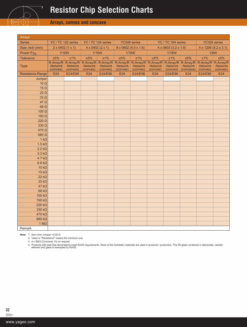
ArraysSeries YC / TC 122 series YC / TC 124 series YC248 series YC / TC 164 series YC324 seriesSize: inch (mm) 2 x 0402 (1 x 1) 4 x 0402 (2 x 1) 8 x 0602 (4.0 x 1.6) 4 x 0603 (3.2 x 1.6) 4 x 1206 (5.2 x 3.1)Power P70 1/16W 1/16W 1/16W 1/16W 1/8WTolerance ±5% ±1% ±5% ±1% ±5% ±1% ±5% ±1% ±5% ±1% ±5%
TypeR-Array/R-Network(convex)
R-Array/R-Network(convex)
R-Array/R-Network(convex)
R-Array/R-Network(convex)
R-Array/R-Network(convex)
R-Array/R-Network(convex)
R-Array/R-Network(convex)
R-Array/R-Network(convex)
R-Array/R-Network(concave)
R-Array/R-Network(convex)
R-Array/R-Network(convex)
Resistance Range E24 E24/E96 E24 E24/E96 E24 E24/E96 E24 E24/E96 E24 E24/E96 E24Jumper
10 Ω15 Ω22 Ω33 Ω47 Ω68 Ω
100 Ω150 Ω220 Ω330 Ω470 Ω680 Ω
1 kΩ1.5 kΩ2.2 kΩ3.3 kΩ4.7 kΩ6.8 kΩ10 kΩ15 kΩ22 kΩ33 kΩ47 kΩ68 kΩ
100 kΩ150 kΩ220 kΩ330 kΩ470 kΩ680 kΩ
1 MΩRemark
Note: 1. Zero ohm Jumper <0.05 Ω2. Value in "Resistance" means the minimum one3. 4 x 0603 (Concave) 1% on request4. Products with lead free terminations meet RoHS requirements. None of the forbidden materials are used in products / production. The Pb-glass contained in electrodes, resistor
element and glass is exempted by RoHS.
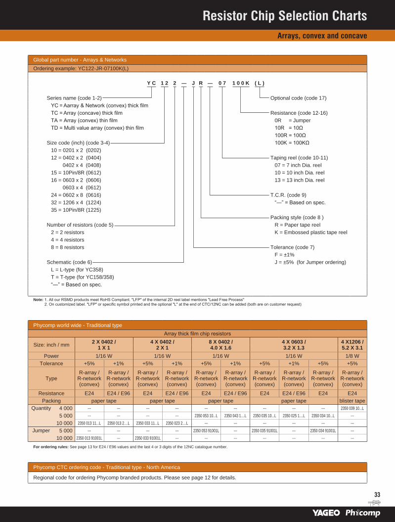
Resistor Chip Selection ChartsArrays, convex and concave
33
Global part number - Arrays & NetworksOrdering example: YC122-JR-07100K(L)
Y C 1 2 2 ― J R ― 0 7 1 0 0 K ( L )
Series name (code 1-2) Optional code (code 17) YC = Aarray & Network (convex) thick filmTC = Array (concave) thick film Resistance (code 12-16)TA = Array (convex) thin film 0R = JumperTD = Multi value array (convex) thin film 10R = 10Ω 100R = 100Ω
Size code (inch) (code 3-4) 100K = 100KΩ10 = 0201 x 2 (0202)12 = 0402 x 2 (0404) Taping reel (code 10-11) 0402 x 4 (0408) 07 = 7 inch Dia. reel15 = 10Pin/8R (0612) 10 = 10 inch Dia. reel16 = 0603 x 2 (0606) 13 = 13 inch Dia. reel 0603 x 4 (0612)24 = 0602 x 8 (0616) T.C.R. (code 9)32 = 1206 x 4 (1224) “―” = Based on spec.35 = 10Pin/8R (1225)
Packing style (code 8 )Number of resistors (code 5) R = Paper tape reel
2 = 2 resistors K = Embossed plastic tape reel4 = 4 resistors8 = 8 resistors Tolerance (code 7)
F = ±1%Schematic (code 6) J = ±5% (for Jumper ordering)
L = L-type (for YC358)T = T-type (for YC158/358)“―” = Based on spec.
Note: 1. All our RSMD products meet RoHS Compliant. "LFP" of the internal 2D reel label mentions "Lead Free Process" 2. On customized label. "LFP" or specific symbol printed and the optional "L" at the end of CTC/12NC can be added (both are on customer request)
Phycomp world wide - Traditional typeArray thick film chip resistors
Size: inch / mm 2 X 0402 / 1 X 1
4 X 0402 / 2 X 1
8 X 0402 / 4.0 X 1.6
4 X 0603 / 3.2 X 1.3
4 X1206 / 5.2 X 3.1
Power 1/16 W 1/16 W 1/16 W 1/16 W 1/8 WTolerance +5% +1% +5% +1% +5% +1% +5% +1% +5% +5%
TypeR-array /
R-network (convex)
R-array / R-network (convex)
R-array / R-network (convex)
R-array / R-network (convex)
R-array / R-network (convex)
R-array / R-network (convex)
R-array / R-network (convex)
R-array / R-network (convex)
R-array / R-network (convex)
R-array / R-network (convex)
Resistance E24 E24 / E96 E24 E24 / E96 E24 E24 / E96 E24 E24 / E96 E24 E24Packing paper tape paper tape paper tape paper tape blister tape
Quantity 4 000 --- --- --- --- --- --- --- --- --- 2350 039 10...L
5 000 --- --- --- --- 2350 053 10...L 2350 043 1....L 2350 035 10...L 2350 025 1....L 2350 034 10...L ---
10 000 2350 013 11...L 2350 013 2....L 2350 033 11...L 2350 023 2....L --- --- --- --- --- ---Jumper 5 000 --- --- --- --- 2350 053 91001L --- 2350 035 91001L --- 2350 034 91001L ---
10 000 2350 013 91001L --- 2350 033 91001L --- --- --- --- --- --- ---
For ordering rules: See page 13 for E24 / E96 values and the last 4 or 3 digits of the 12NC catalogue number.
Phycomp CTC ordering code - Traditional type - North America
Regional code for ordering Phycomp branded products. Please see page 12 for details.
Resistor Chip Selection ChartsArrays, convex and concave
34
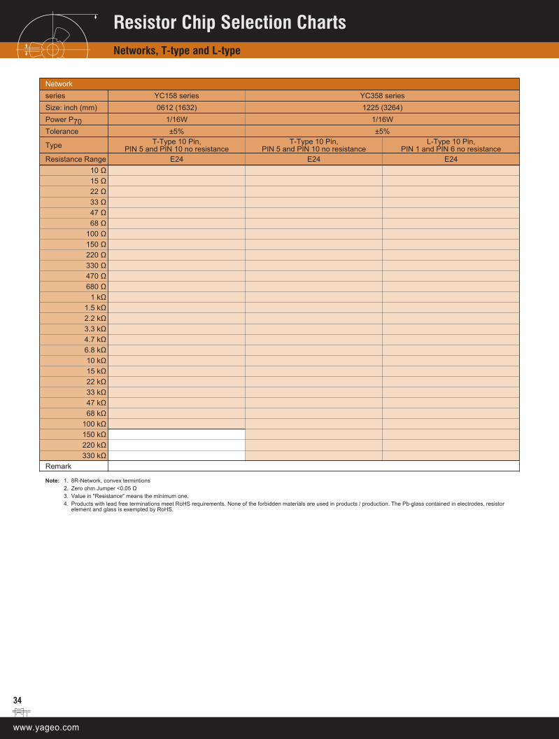
Networkseries YC158 series YC358 seriesSize: inch (mm) 0612 (1632) 1225 (3264)Power P70 1/16W 1/16WTolerance ±5% ±5%
Type T-Type 10 Pin,PIN 5 and PIN 10 no resistance
T-Type 10 Pin,PIN 5 and PIN 10 no resistance
L-Type 10 Pin,PIN 1 and PIN 6 no resistance
Resistance Range E24 E24 E2410 Ω15 Ω22 Ω33 Ω47 Ω68 Ω
100 Ω150 Ω220 Ω330 Ω470 Ω680 Ω
1 kΩ1.5 kΩ2.2 kΩ3.3 kΩ4.7 kΩ6.8 kΩ10 kΩ15 kΩ22 kΩ33 kΩ47 kΩ68 kΩ
100 kΩ150 kΩ220 kΩ330 kΩ
Remark
Note: 1. 8R-Network, convex termintions2. Zero ohm Jumper <0.05 Ω3. Value in "Resistance" means the minimum one.4. Products with lead free terminations meet RoHS requirements. None of the forbidden materials are used in products / production. The Pb-glass contained in electrodes, resistor
element and glass is exempted by RoHS.
Resistor Chip Selection ChartsNetworks, T-type and L-type

35
Global part number - Arrays & NetworksOrdering example: YC158TJR-07100K(L)
Y C 1 5 8 T J R ― 0 7 1 0 0 K ( L )
Series name (code 1-2) Optional code (code 17) YC = Aarray & Network (convex) thick filmTC = Array (concave) thick film Resistance (code 12-16)
0R = JumperSize code (inch) (code 3-4) 10R = 10Ω
10 = 0201 x 2 (0202) 100R = 100Ω12 = 0402 x 2 (0404) 100K = 100KΩ 0402 x 4 (0408)15 = 10Pin/8R (0612) Taping reel (code 10-11)16 = 0603 x 2 (0606) 07 = 7 inch Dia. reel 0603 x 4 (0612) 13 = 13 inch Dia. reel24 = 0602 x 8 (0616)32 = 1206 x 4 (1224) T.C.R. (code 9)35 = 10Pin/8R (1225) “―” = Based on spec.
Number of resistors (code 5) Packing style (code 8 )2 = 2 resistors R = Paper tape reel4 = 4 resistors K = Embossed plastic tape reel8 = 8 resistors
Tolerance (code 7)Schematic (code 6) F = ±1%
L = L-type (for YC358) J = ±5% (for Jumper ordering)T = T-type (for YC158/358)“―” = Based on spec.
Note: 1. All our RSMD products meet RoHS Compliant. "LFP" of the internal 2D reel label mentions "Lead Free Process" 2. On customized label. "LFP" or specific symbol printed and the optional "L" at the end of CTC/12NC can be added (both are on customer request)
Phycomp world wide - Traditional type Network thick film chip resistors
Size: inch (mm) 0612 (1632) 1225 (3264)Power 1/32 W 1/16 W
Tolerance +5% +5%
Type T-type 10 Pin / 8R PIN 5 and PIN 10 no resistance
T-type 10 Pin / 8R PIN 5 and PIN 10 no resistance
L-type 10 Pin / 8R PIN 1 and PIN 6 no resistance
Resistance E24 E24 E24Packing paper tape blister tape
Quantity 4 000 --- 2350 201 10...L 2350 200 10...L 5 000 2350 230 10...L --- ---
For ordering rules: See page 13 for E24 / E96 values and the last 4 or 3 digits of the 12NC catalogue number.
Phycomp CTC ordering code - Traditional type - North America
Regional code for ordering Phycomp branded products. Please see page 12 for details.
Resistor Chip Selection ChartsNetworks, T-type and L-type
36
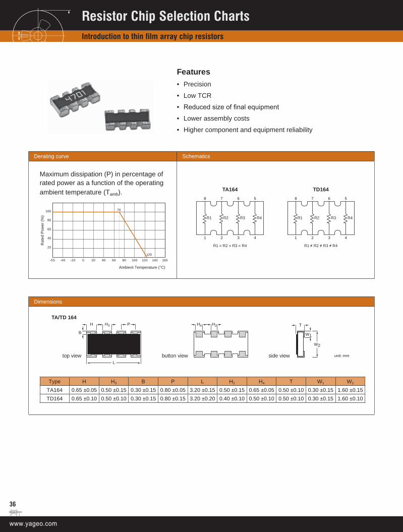
FeaturesPrecision
Low TCR
Reduced size of final equipment
Lower assembly costs
Higher component and equipment reliability
•
•
•
•
•
Derating curve Schematics
Maximum dissipation (P) in percentage of rated power as a function of the operating ambient temperature (Tamb).
100
80
60
40
20
-55 -40 -20 0 20 40 60 80
70
100 120 140 160
Ambient Temperature (°C)
Ra
ted
Po
we
r (%
)
125
TA164
8 7 6 5
1 2 3 4
R1 R2 R3 R4
TD164
8 7 6 5
1 2 3 4
R1 R2 R3 R4
R1 = R2 = R3 = R4 R1 R2 R3 R4
Dimensions
TA/TD 164
H H3
B
P
L
top view
H4 H2
button view
T
W1
W2
side view unit: mm
Type H H3 B P L H2 H4 T W1 W2
TA164 0.65 ±0.05 0.50 ±0.15 0.30 ±0.15 0.80 ±0.05 3.20 ±0.15 0.50 ±0.15 0.65 ±0.05 0.50 ±0.10 0.30 ±0.15 1.60 ±0.15TD164 0.65 ±0.10 0.50 ±0.10 0.30 ±0.15 0.80 ±0.15 3.20 ±0.20 0.40 ±0.10 0.50 ±0.10 0.50 ±0.10 0.30 ±0.15 1.60 ±0.10
Resistor Chip Selection ChartsIntroduction to thin film array chip resistors

37
Electrical characteristics
Type Power P70
Operating Temp. range MWV RCOV DWV Resistance range & tolerance T. C. R.
( ppm/°C)
TA164 1/16W -55°C to +125°C 75V 150V 150V E24/E96 ±0.1%, ±0.5%, ±1% 10Ω ≤ R ≤ 330KΩ ±25±50TD164 1/16W -55°C to +125°C 75V 150V 150V E24/E96 ±0.1%, ±0.5%, ±1% 10Ω ≤ R ≤ 330KΩ
Note: See page 11 for ordering code. For more detailed, please contact with sales offices, distributors and representatives in your region.
Environmental characteristicsPerformance test Test method Procedure Requirements
Life MIL-STD-202G-method 108A
1 000 hours at 70 ±5°C applied RCWV 1.5 hours on, 0.5 hours off, still air required
±(0.25% +0.05Ω) for TD164 ±(0.5% +0.05Ω) for TA164
High temperature exposure
MIL-STD-202G-method 108A
1 000 hours at maximum operating temperature depending on specification, unpowered
Satisfy electrical and physical characteristic
Moisture resistance MIL-STD-202G-method 106F
Each temperature / humidity cycle is defined at 8 hours (method 106F), 3 cycles / 24 hours for 10d with 25°C / 65°C 95% R.H ±(0.25% +0.05Ω) for TD164
±(0.5% +0.05Ω) for TA164
Thermal shock MIL-STD-202G-method 107G
LCT / UCT, number of cycles required is 300Maximum transfer time is 20 seconds
Solderability Wetting IPC/JEDECJ-
STD-002B testB
Electrical test not required. Magnification 50X Leadfree solder bath at 245 ±3°C Dipping time: 3 ±0.5 seconds
Well tinned (≥95% covered)
Resistance to soldering heat
MIL-STD-202G-method 210F Leadfree solder, 270°C, 10 seconds immersion time Satisfy electrical and
physical characteristic
Short time overload MIL-R-55342D-para 4.7.5
2.5 times RCWV or maximum overload voltage which-ever is less for 5 seconds at room temperature
±(0.25% +0.05Ω) for TD164 ±(0.5% +0.05Ω) for TA164
Resistor Chip Selection ChartsIntroduction to thin film array chip resistors
38
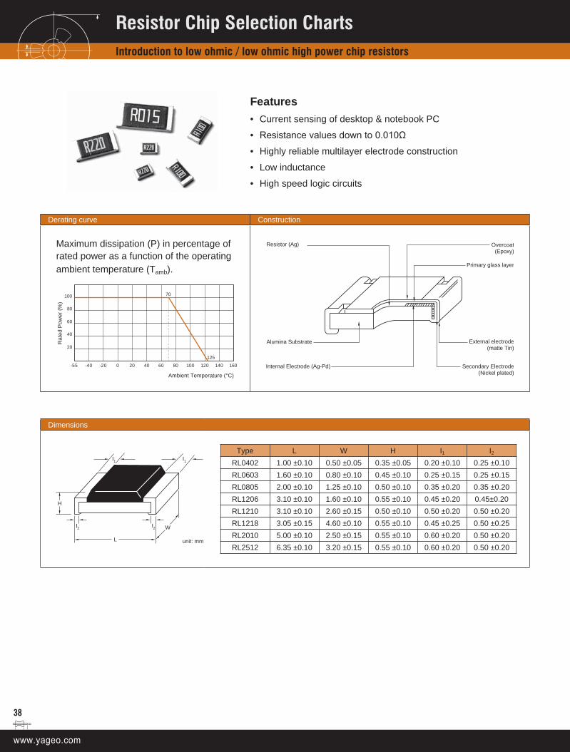
FeaturesCurrent sensing of desktop & notebook PC
Resistance values down to 0.010Ω
Highly reliable multilayer electrode construction
Low inductance
High speed logic circuits
•
•
•
•
•
Derating curve Construction
Maximum dissipation (P) in percentage of rated power as a function of the operating ambient temperature (Tamb).
100
80
60
40
20
-55 -40 -20 0 20 40 60 80
70
100 120 140 160
Ambient Temperature (°C)
Ra
ted
Po
we
r (%
)
125
Overcoat(Epoxy)
Primary glass layer
Secondary Electrode (Nickel plated)
External electrode(matte Tin)
Resistor (Ag)
Alumina Substrate
Internal Electrode (Ag-Pd)
Dimensions
W
unit: mm
I2
I2
I1
I1
L
H
Type L W H I1 I2RL0402 1.00 ±0.10 0.50 ±0.05 0.35 ±0.05 0.20 ±0.10 0.25 ±0.10RL0603 1.60 ±0.10 0.80 ±0.10 0.45 ±0.10 0.25 ±0.15 0.25 ±0.15RL0805 2.00 ±0.10 1.25 ±0.10 0.50 ±0.10 0.35 ±0.20 0.35 ±0.20RL1206 3.10 ±0.10 1.60 ±0.10 0.55 ±0.10 0.45 ±0.20 0.45±0.20RL1210 3.10 ±0.10 2.60 ±0.15 0.50 ±0.10 0.50 ±0.20 0.50 ±0.20RL1218 3.05 ±0.15 4.60 ±0.10 0.55 ±0.10 0.45 ±0.25 0.50 ±0.25RL2010 5.00 ±0.10 2.50 ±0.15 0.55 ±0.10 0.60 ±0.20 0.50 ±0.20RL2512 6.35 ±0.10 3.20 ±0.15 0.55 ±0.10 0.60 ±0.20 0.50 ±0.20
Resistor Chip Selection ChartsIntroduction to low ohmic / low ohmic high power chip resistors
39
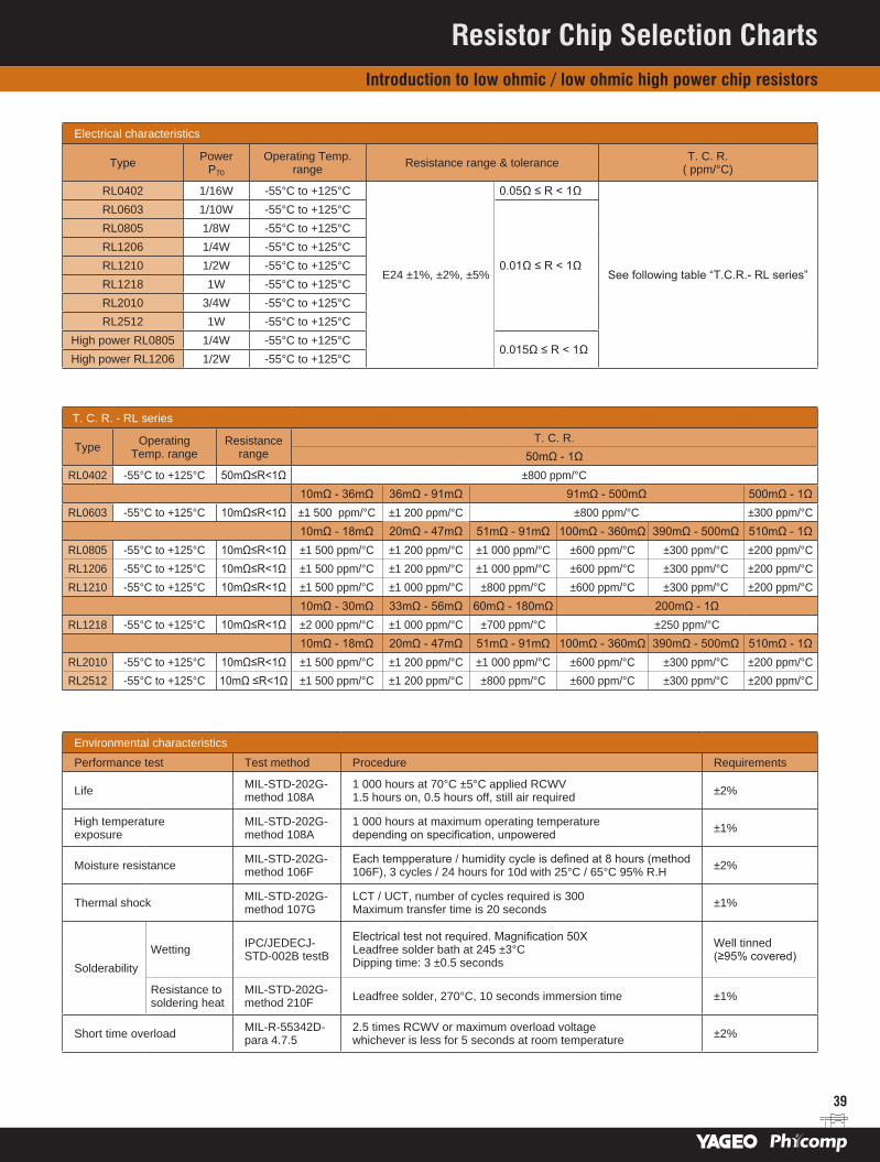
Electrical characteristics
Type Power P70
Operating Temp. range Resistance range & tolerance T. C. R.
( ppm/°C)
RL0402 1/16W -55°C to +125°C
E24 ±1%, ±2%, ±5%
0.05Ω ≤ R < 1Ω
See following table “T.C.R.- RL series”
RL0603 1/10W -55°C to +125°C
0.01Ω ≤ R < 1Ω
RL0805 1/8W -55°C to +125°CRL1206 1/4W -55°C to +125°CRL1210 1/2W -55°C to +125°CRL1218 1W -55°C to +125°CRL2010 3/4W -55°C to +125°CRL2512 1W -55°C to +125°C
High power RL0805 1/4W -55°C to +125°C0.015Ω ≤ R < 1Ω
High power RL1206 1/2W -55°C to +125°C
T. C. R. - RL series
Type Operating Temp. range
Resistance range
T. C. R.50mΩ - 1Ω
RL0402 -55°C to +125°C 50mΩ≤R<1Ω ±800 ppm/°C10mΩ - 36mΩ 36mΩ - 91mΩ 91mΩ - 500mΩ 500mΩ - 1Ω
RL0603 -55°C to +125°C 10mΩ≤R<1Ω ±1 500 ppm/°C ±1 200 ppm/°C ±800 ppm/°C ±300 ppm/°C10mΩ - 18mΩ 20mΩ - 47mΩ 51mΩ - 91mΩ 100mΩ - 360mΩ 390mΩ - 500mΩ 510mΩ - 1Ω
RL0805 -55°C to +125°C 10mΩ≤R<1Ω ±1 500 ppm/°C ±1 200 ppm/°C ±1 000 ppm/°C ±600 ppm/°C ±300 ppm/°C ±200 ppm/°CRL1206 -55°C to +125°C 10mΩ≤R<1Ω ±1 500 ppm/°C ±1 200 ppm/°C ±1 000 ppm/°C ±600 ppm/°C ±300 ppm/°C ±200 ppm/°CRL1210 -55°C to +125°C 10mΩ≤R<1Ω ±1 500 ppm/°C ±1 000 ppm/°C ±800 ppm/°C ±600 ppm/°C ±300 ppm/°C ±200 ppm/°C
10mΩ - 30mΩ 33mΩ - 56mΩ 60mΩ - 180mΩ 200mΩ - 1ΩRL1218 -55°C to +125°C 10mΩ≤R<1Ω ±2 000 ppm/°C ±1 000 ppm/°C ±700 ppm/°C ±250 ppm/°C
10mΩ - 18mΩ 20mΩ - 47mΩ 51mΩ - 91mΩ 100mΩ - 360mΩ 390mΩ - 500mΩ 510mΩ - 1ΩRL2010 -55°C to +125°C 10mΩ≤R<1Ω ±1 500 ppm/°C ±1 200 ppm/°C ±1 000 ppm/°C ±600 ppm/°C ±300 ppm/°C ±200 ppm/°CRL2512 -55°C to +125°C 10mΩ ≤R<1Ω ±1 500 ppm/°C ±1 200 ppm/°C ±800 ppm/°C ±600 ppm/°C ±300 ppm/°C ±200 ppm/°C
Environmental characteristics
Performance test Test method Procedure Requirements
Life MIL-STD-202G-method 108A
1 000 hours at 70°C ±5°C applied RCWV 1.5 hours on, 0.5 hours off, still air required ±2%
High temperature exposure
MIL-STD-202G-method 108A
1 000 hours at maximum operating temperature depending on specification, unpowered ±1%
Moisture resistance MIL-STD-202G-method 106F
Each tempperature / humidity cycle is defined at 8 hours (method 106F), 3 cycles / 24 hours for 10d with 25°C / 65°C 95% R.H ±2%
Thermal shock MIL-STD-202G-method 107G
LCT / UCT, number of cycles required is 300 Maximum transfer time is 20 seconds ±1%
Solderability Wetting IPC/JEDECJ-
STD-002B testB
Electrical test not required. Magnification 50X Leadfree solder bath at 245 ±3°C Dipping time: 3 ±0.5 seconds
Well tinned (≥95% covered)
Resistance to soldering heat
MIL-STD-202G-method 210F Leadfree solder, 270°C, 10 seconds immersion time ±1%
Short time overload MIL-R-55342D-para 4.7.5
2.5 times RCWV or maximum overload voltagewhichever is less for 5 seconds at room temperature ±2%
Resistor Chip Selection ChartsIntroduction to low ohmic / low ohmic high power chip resistors

40
Low ohmic / RL seriesSize: inch (mm) 0402 (1005) 0603 (1608) 0805 (2012) 1206 (3216)Power P70 1/16W 1/10W 1/8W 1/4WTolerance ±5% ±1% ±5% ±1% ±5% ±1% ±5% ±1%Resistance Range E24 E24 E24 E24 E24 E24 E24 E24
0.01 Ω0.02 Ω0.03 Ω0.04 Ω0.05 Ω0.06 Ω0.07 Ω0.08 Ω0.09 Ω
0.1 Ω0.2 Ω0.3 Ω0.4 Ω0.5 Ω0.6 Ω0.7 Ω0.8 Ω0.9 Ω
Remark
Note: 1. Value in "Resistance" means the minimum one2. E48/E96 on request3. The partial values of 25 / 40 / 50 / 60 / 250 / 400 / 500 mΩ are also available4. Products with lead free terminations meet RoHS requirements. None of the forbidden materials are used in products / production. The Pb-glass contained in electrodes, resistor
element and glass is exempted by RoHS.
Resistor Chip Selection ChartsLow ohmic, 0201 to 1206

41
Global part number - Preferred type
Ordering example: RL0603JR-070R01(L)
R L 0 6 0 3 J R ― 0 7 0 R 0 1 ( L )
Series name (code 1-2) Optional code(1/2) (code 17) RL = Low ohmic
Resistance (code 12-16)Size code (code 3-6) 0R01 = 0.01Ω
(inch / metric) 0R1 = 0.1Ω0402 = 1.0 x 0.5 0R2 = 0.2Ω0603 = 1.6 x 0.80805 = 2.0 x 1.25 Taping reel (code 10-11)1206 = 3.2 x 1.6 07 = 7 inch Dia. reel1210 = 3.2 x 2.6 10 = 10 inch Dia. reel1218 = 3.2 x 4.5 13 = 13 inch Dia. reel2010 = 5.0 x 2.52512 = 6.35 x 3.2 T. C. R. (code 9)
“―” = Based on spec.Tolerance (code 7) (― for thick film only)
F = ±1% G = ±2% Packing style (code 8 ) J = ±5% (for Jumper ordering) R = Paper tape reel
K = Embossed plastic tape reel
Note: 1. All our RSMD products meet RoHS Compliant. "LFP" of the internal 2D reel label mentions "Lead Free Process" 2. On customized label. "LFP" or specific symbol printed and the optional "L" at the end of CTC/12NC can be added (both are on customer request)
Phycomp world wide - Traditional typeLow ohmic chip resistors
Size: inch (mm) 0402 (1005) 0603 (1608) 0805 (2012) 1206 (3216)Power 1/16 W 1/10 W 1/8 W 1/4 W
Tolerance +5% +1% +5% +1% +5% +1% +5% +1%Resistance E24 E24 E24 E24 E24 E24 E24 E24
Packing paper tape paper tape paper tape paper tapeQuantity 5 000 --- --- 2350 512 10…L 2350 512 12…L 2350 511 10…L 2350 511 12…L 2350 510 10…L 2350 510 12…L
10 000 2350 513 20…L 2350 513 22…L --- --- --- --- --- ---
For ordering rules: See page 13 for E24 / E96 values and the last 4 or 3 digits of the 12NC catalogue number.
Phycomp CTC ordering code - Traditional type - North America
Regional code for ordering Phycomp branded products. Please see page 12 for details.
Resistor Chip Selection ChartsLow ohmic, 0201 to 1206
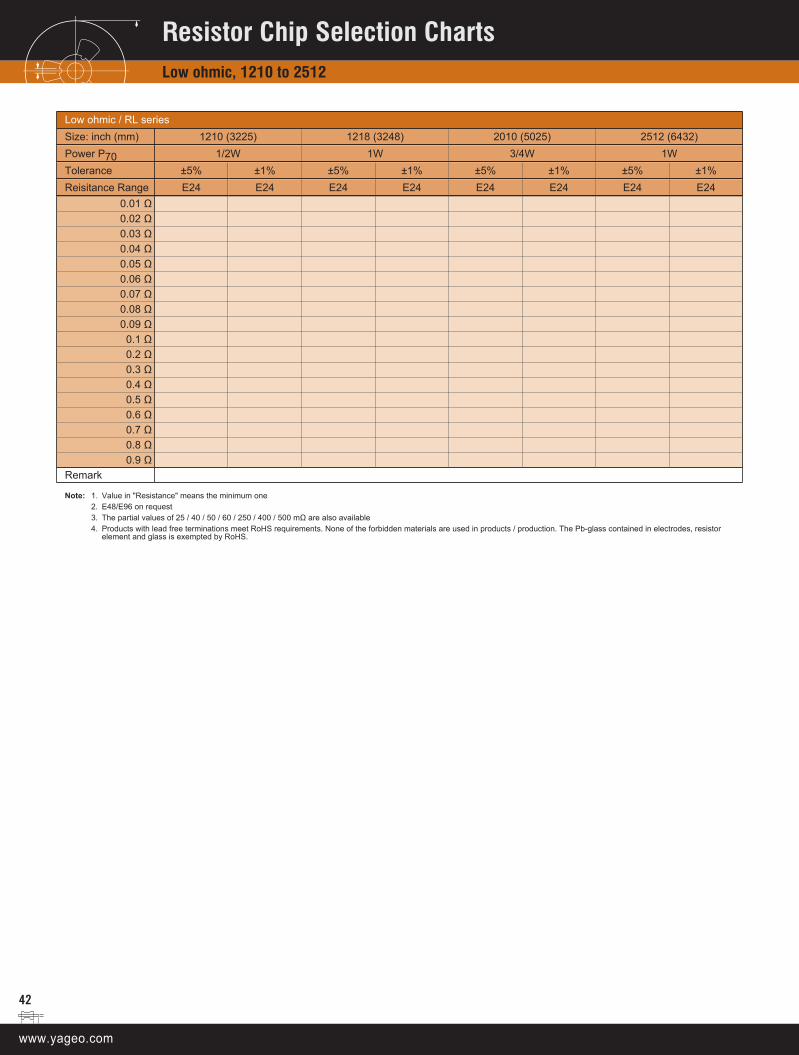
42
Low ohmic / RL seriesSize: inch (mm) 1210 (3225) 1218 (3248) 2010 (5025) 2512 (6432)Power P70 1/2W 1W 3/4W 1WTolerance ±5% ±1% ±5% ±1% ±5% ±1% ±5% ±1%Reisitance Range E24 E24 E24 E24 E24 E24 E24 E24
0.01 Ω0.02 Ω0.03 Ω0.04 Ω0.05 Ω0.06 Ω0.07 Ω0.08 Ω0.09 Ω
0.1 Ω0.2 Ω0.3 Ω0.4 Ω0.5 Ω0.6 Ω0.7 Ω0.8 Ω0.9 Ω
Remark
Note: 1. Value in "Resistance" means the minimum one2. E48/E96 on request3. The partial values of 25 / 40 / 50 / 60 / 250 / 400 / 500 mΩ are also available4. Products with lead free terminations meet RoHS requirements. None of the forbidden materials are used in products / production. The Pb-glass contained in electrodes, resistor
element and glass is exempted by RoHS.
Resistor Chip Selection ChartsLow ohmic, 1210 to 2512

43
Global part number - Preferred type
Ordering example: RL1210JR-070R01(L)
R L 1 2 1 0 J R ― 0 7 0 R 0 1 ( L )
Series name (code 1-2) Optional code(1/2) (code 17) RL = Low ohmic
Resistance (code 12-16)Size code (code 3-6) 0R01 = 0.01Ω
(inch / metric) 0R1 = 0.1Ω0402 = 1.0 x 0.5 0R2 = 0.2Ω0603 = 1.6 x 0.80805 = 2.0 x 1.25 Taping reel (code 10-11)1206 = 3.2 x 1.6 07 = 7 inch Dia. reel1210 = 3.2 x 2.61218 = 3.2 x 4.5 T. C. R. (code 9)2010 = 5.0 x 2.5 “―” = Based on spec.2512 = 6.35 x 3.2 (― for thick film only)
Tolerance (code 7) Packing style (code 8 ) F = ±1% R = Paper tape reel G = ±2% K = Embossed plastic tape reel J = ±5% (for Jumper ordering)
Note: 1. All our RSMD products meet RoHS Compliant. "LFP" of the internal 2D reel label mentions "Lead Free Process" 2. On customized label. "LFP" or specific symbol printed and the optional "L" at the end of CTC/12NC can be added (both are on customer request)
Phycomp world wide - Traditional typeLow ohmic chip resistors
Size: inch (mm) 1210 (3225) 1218 (3248) 2010 (5025) 2512 (6432)Power 1/2 W 1 W 3/4 W 1 W
Tolerance +5% +1% +5% +1% +5% +1% +5% +1%Resistance E24 E24 E24 E24 E24 E24 E24 E24
Packing paper tape blister tape blister tape blister tapeQuantity 4 000 --- --- 2322 735 64…L 2322 735 7….L 2322 760 90..0L/60..7L 2322 761 90..0L/6...7L 2322 762 90..0L/60..7L 2322 763 90..0L/6...7L
5 000 2390 735 90..0L/60..7L 2390 735 3….L --- --- --- --- --- ---
For ordering rules: See page 13 for E24 / E96 values and the last 4 or 3 digits of the 12NC catalogue number.
Phycomp CTC ordering code - Traditional type - North America
Regional code for ordering Phycomp branded products. Please see page 12 for details.
Resistor Chip Selection ChartsLow ohmic, 1210 to 2512
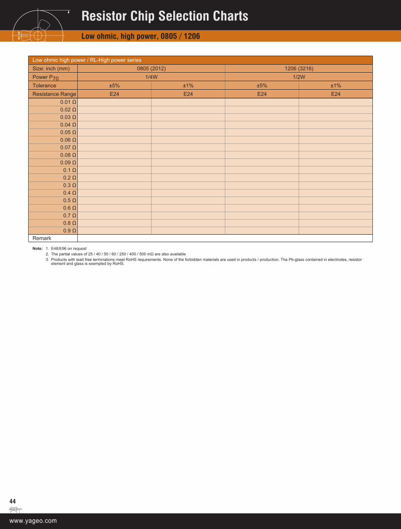
44
Low ohmic high power / RL-High power seriesSize: inch (mm) 0805 (2012) 1206 (3216)Power P70 1/4W 1/2WTolerance ±5% ±1% ±5% ±1%Resistance Range E24 E24 E24 E24
0.01 Ω0.02 Ω0.03 Ω0.04 Ω0.05 Ω0.06 Ω0.07 Ω0.08 Ω0.09 Ω
0.1 Ω0.2 Ω0.3 Ω0.4 Ω0.5 Ω0.6 Ω0.7 Ω0.8 Ω0.9 Ω
Remark
Note: 1. E48/E96 on request2. The partial values of 25 / 40 / 50 / 60 / 250 / 400 / 500 mΩ are also available3. Products with lead free terminations meet RoHS requirements. None of the forbidden materials are used in products / production. The Pb-glass contained in electrodes, resistor
element and glass is exempted by RoHS.
Resistor Chip Selection ChartsLow ohmic, high power, 0805 / 1206

45
Global part number - Preferred typeOrdering example: RL0805JR-7W0R01(L)
R L 0 8 0 5 J R ― 7 W 0 R 0 1 ( L )
Series name (code 1-2) Optional code (code 17) RL = Low ohmic
Resistance (code 12-16)Size code (code 3-6) 0R01 = 0.01Ω
(inch / metric) 0R1 = 0.1Ω0805 = 2.0 x 1.25 0R2 = 0.2Ω1206 = 3.2 x 1.6
Taping reel (code 10-11)Tolerance (code 7) 7W = 7 inch Dia. reel and
2 x standard power type F = ±1% G = ±2% J = ±5% T. C. R. (code 9)
“―” = Based on spec.Packing style (code 8 ) (― for thick film only)
R = Paper tape reel
Note: 1. All our RSMD products meet RoHS Compliant. "LFP" of the internal 2D reel label mentions "Lead Free Process" 2. On customized label. "LFP" or specific symbol printed and the optional "L" at the end of CTC/12NC can be added (both are on customer request)
Phycomp world wide - Traditional typeLow ohmic high power chip resistors
Size: inch (mm) 0805 (2012) 1206 (3216)Power 1/4 W 1/2 W
Tolerance +5% +1% +5% +1%Resistance E24 E24 / E96 E24 E24 / E96
Packing paper tape paper tapeQuantity 5 000 2350 511 15…L 2350 511 17…L 2350 519 01…L 2350 519 1.…L
For ordering rules: See page 13 for E24 / E96 values and the last 4 or 3 digits of the 12NC catalogue number.
Phycomp CTC ordering code - Traditional type - North America
Regional code for ordering Phycomp branded products. Please see page 12 for details.
Resistor Chip Selection ChartsLow ohmic, high power, 0805 / 1206
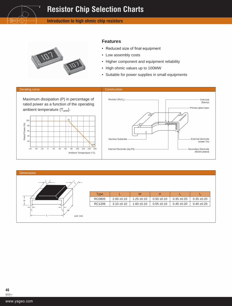
46
FeaturesReduced size of final equipment
Low assembly costs
Higher component and equipment reliability
High ohmic values up to 100MW
Suitable for power supplies in small equipments
•
•
•
•
•
Derating curve Construction
Maximum dissipation (P) in percentage of rated power as a function of the operating ambient temperature (Tamb).
100
80
60
40
20
-55 -40 -20 0 20 40 60 80
70
100 120 140 160
Ambient Temperature (°C)
Ra
ted
Po
we
r (%
)
155
Overcoat(Epoxy)
Primary glass layer
Secondary Electrode (Nickel plated)
External electrode(matte Tin)
Resistor (RuO2)
Alumina Substrate
Internal Electrode (Ag-Pd)
Dimensions
W
unit: mm
I2
I2
I1
I1
L
H
Type L W H I1 I2RC0805 2.00 ±0.10 1.25 ±0.10 0.50 ±0.10 0.35 ±0.20 0.35 ±0.20RC1206 3.10 ±0.10 1.60 ±0.10 0.55 ±0.10 0.45 ±0.20 0.40 ±0.20
Resistor Chip Selection ChartsIntroduction to high ohmic chip resistors

47
Electrical characteristics
Type Power P70
Operating Temp. range MWV RCOV DWV Resistance range & tolerance T. C. R.
( ppm/°C)
RC0805 1/8W -55°C to +155°C 150V 300V 300VE24 ±5%, ±10%, ±20% 24MΩ ≤ R ≤ 100MΩ ±300
RC1206 1/4W -55°C to +155°C 200V 400V 500VNote: See page 10 for ordering code. For more detailed, please contact with sales offices, distributors and representatives in your region.
Environmental characteristics
Performance test Test method Procedure Requirements
Life MIL-STD-202G-method 108A
1 000 hours at 70 ±5°C applied RCWV 1.5 hours on, 0.5 hours off, still air required ±(2% +0.05Ω)
High temperature exposure MIL-STD-202G-method 108A
1 000 hours at maximum operating temperature depending on specification, unpowered ±(1% +0.05Ω)
Moisture resistance MIL-STD-202G-method 106F
Each temperature / humidity cycle is defined at 8 hours (method 106F), 3 cycles / 24 hours for 10d with 25°C / 65°C 95% R.H ±(2% +0.05Ω)
Thermal shock MIL-STD-202G-method 107G
LCT / UCT, number of cycles required is 300 Maximum transfer time is 20 seconds
±(0.5% +0.05Ω) ±(1% +0.05Ω)
Solderability Wetting IPC/JEDECJ-
STD-002B testB
Electrical test not required. Magnification 50X Leadfree solder bath at 245 ±3°C Dipping time: 3 ±0.5 seconds
Well tinned (≥95% covered)
Resistance to soldering heat
MIL-STD-202G-method 210F Leadfree solder, 270°C, 10 seconds immersion time ±(1% +0.05Ω)
Short time overload MIL-R-55342D-para 4.7.5
2.5 times RCWV or maximum overload voltage which-ever is less for 5 seconds at room temperature ±(2% +0.05Ω)
Resistor Chip Selection ChartsIntroduction to high ohmic chip resistors

48
FeaturesNew Ni/Au terminations provide special application for hybrid board gluing
Competitive with AgPd terminations
Special use in high temperature environment
Higher component and equipment reliability
•
•
•
•
Derating curve Construction
Maximum dissipation (P) in percentage of rated power as a function of the operating ambient temperature (Tamb).
100
80
60
40
20
-55 -40 -20 0 20 40 60 80
70
100 120 140 160
Ambient Temperature (°C)
Ra
ted
Po
we
r (%
)
155
Overcoat(Epoxy)
Primary glass layer
Secondary Electrode (Nickel plated)
External electrode(matte Tin)
Resistor (RuO2)
(Jumper chip is a conductor)
Alumina Substrate
Internal Electrode (Ag-Pd)
Dimensions
W
unit: mm
I2
I2
I1
I1
L
H
Type L W H I1 I2AR0402 1.00 ±0.05 0.50 ±0.05 0.35 ±0.05 0.20 ±0.10 0.25 ±0.10AR0603 1.60 ±0.10 0.80 ±0.10 0.45 ±0.10 0.25 ±0.15 0.25 ±0.15AR0805 2.00 ±0.10 1.25 ±0.10 0.50 ±0.10 0.35 ±0.20 0.35 ±0.20AR1206 3.10 ±0.10 1.60 ±0.10 0.55 ±0.10 0.45 ±0.20 0.40 ±0.20
Resistor Chip Selection ChartsIntroduction to Ni/Au terminations chip resistors
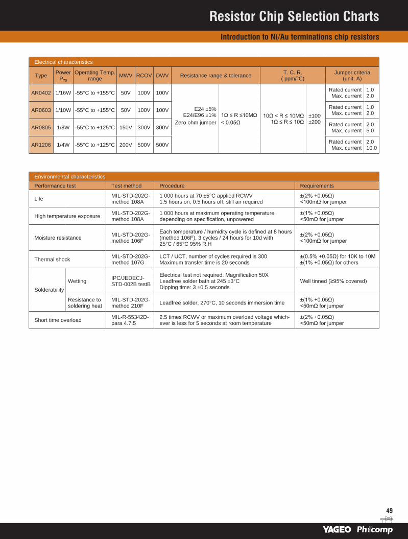
49
Electrical characteristics
Type Power P70
Operating Temp. range MWV RCOV DWV Resistance range & tolerance T. C. R.
( ppm/°C)Jumper criteria
(unit: A)
AR0402 1/16W -55°C to +155°C 50V 100V 100V
E24 ±5% E24/E96 ±1% 1Ω ≤ R ≤10MΩ 10Ω < R ≤ 10MΩ
1Ω ≤ R ≤ 10Ω±100 ±200
Rated current Max. current
1.0 2.0
AR0603 1/10W -55°C to +155°C 50V 100V 100V Rated current Max. current
1.0 2.0
AR0805 1/8W -55°C to +125°C 150V 300V 300VZero ohm jumper < 0.05Ω Rated current
Max. current 2.0 5.0
AR1206 1/4W -55°C to +125°C 200V 500V 500V Rated current Max. current
2.0 10.0
Environmental characteristics
Performance test Test method Procedure Requirements
Life MIL-STD-202G-method 108A
1 000 hours at 70 ±5°C applied RCWV 1.5 hours on, 0.5 hours off, still air required
±(2% +0.05Ω) <100mΩ for jumper
High temperature exposure MIL-STD-202G-method 108A
1 000 hours at maximum operating temperature depending on specification, unpowered
±(1% +0.05Ω) <50mΩ for jumper
Moisture resistance MIL-STD-202G-method 106F
Each temperature / humidity cycle is defined at 8 hours (method 106F), 3 cycles / 24 hours for 10d with 25°C / 65°C 95% R.H
±(2% +0.05Ω) <100mΩ for jumper
Thermal shock MIL-STD-202G-method 107G
LCT / UCT, number of cycles required is 300 Maximum transfer time is 20 seconds
±(0.5% +0.05Ω) for 10K to 10M ±(1% +0.05Ω) for others
Solderability Wetting IPC/JEDECJ-
STD-002B testB
Electrical test not required. Magnification 50X Leadfree solder bath at 245 ±3°C Dipping time: 3 ±0.5 seconds
Well tinned (≥95% covered)
Resistance to soldering heat
MIL-STD-202G-method 210F Leadfree solder, 270°C, 10 seconds immersion time ±(1% +0.05Ω)
<50mΩ for jumper
Short time overload MIL-R-55342D-para 4.7.5
2.5 times RCWV or maximum overload voltage which-ever is less for 5 seconds at room temperature
±(2% +0.05Ω) <50mΩ for jumper
Resistor Chip Selection ChartsIntroduction to Ni/Au terminations chip resistors

50
Chip resistors with NiAu terminations / AR seriesSize: inch (mm) 0402 (1005) 0603 (1608) 0805 (2012) 1206 (3216)Power P70 1/16W 1/10W 1/8W 1/4WTolerance ±5% ±1% ±5% ±1% ±5% ±1% ±5% ±1%Resistance Range E24 E24/E96 E24 E24/E96 E24 E24/E96 E24 E24/E96
Jumper1 Ω
1.5 Ω2.2 Ω3.3 Ω4.7 Ω6.8 Ω10 Ω15 Ω22 Ω33 Ω47 Ω68 Ω
100 Ω150 Ω220 Ω330 Ω470 Ω680 Ω
1 kΩ1.5 kΩ2.2 kΩ3.3 kΩ4.7 kΩ6.8 kΩ10 kΩ15 kΩ22 kΩ33 kΩ47 kΩ68 kΩ
100 kΩ150 kΩ220 kΩ330 kΩ470 kΩ680 kΩ
1 MΩ1.5 MΩ2.2 MΩ3.3 MΩ4.7 MΩ6.8 MΩ10 MΩ
Remark
Note: 1. Zero ohm Jumper <0.05 Ω2. Value in "Resistance" means the minimum one3. Products with lead free terminations meet RoHS requirements. None of the forbidden materials are used in products / production. The Pb-glass contained in electrodes, resistor
element and glass is exempted by RoHS.
Resistor Chip Selection Charts0402 to 1206
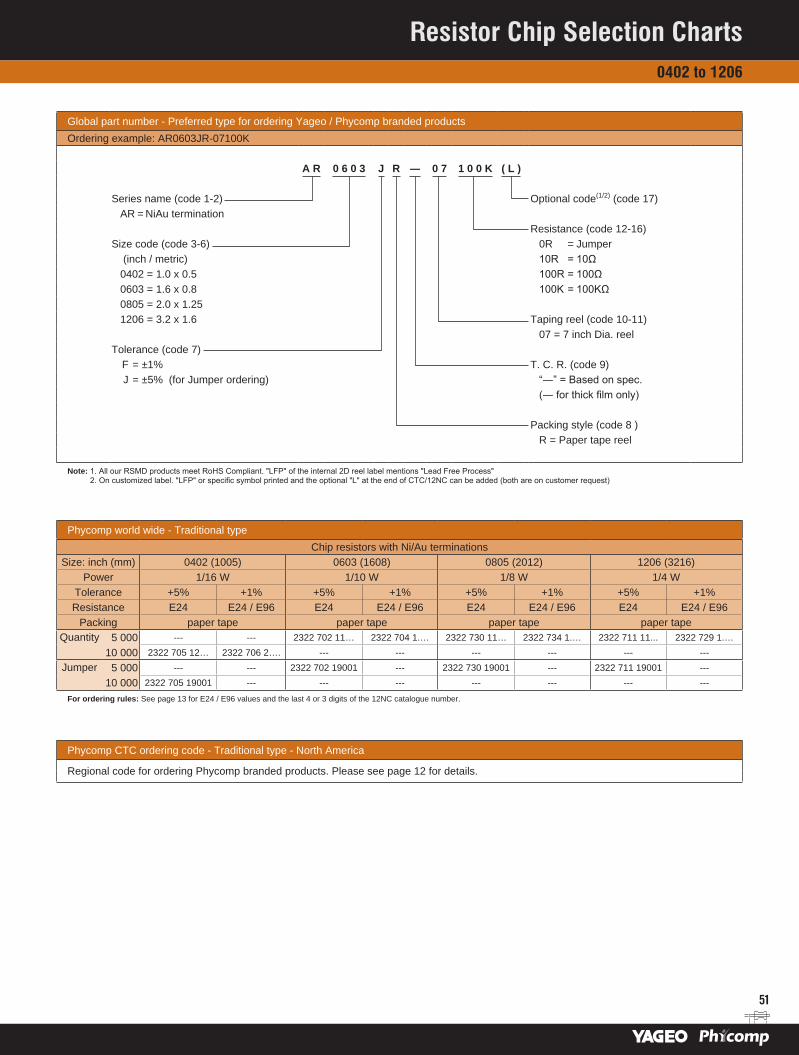
51
Global part number - Preferred type for ordering Yageo / Phycomp branded productsOrdering example: AR0603JR-07100K
A R 0 6 0 3 J R ― 0 7 1 0 0 K ( L )
Series name (code 1-2) Optional code(1/2) (code 17) AR = NiAu termination
Resistance (code 12-16)Size code (code 3-6) 0R = Jumper
(inch / metric) 10R = 10Ω0402 = 1.0 x 0.5 100R = 100Ω0603 = 1.6 x 0.8 100K = 100KΩ0805 = 2.0 x 1.251206 = 3.2 x 1.6 Taping reel (code 10-11)
07 = 7 inch Dia. reelTolerance (code 7)
F = ±1% T. C. R. (code 9) J = ±5% (for Jumper ordering) “―” = Based on spec.
(― for thick film only)
Packing style (code 8 )R = Paper tape reel
Note: 1. All our RSMD products meet RoHS Compliant. "LFP" of the internal 2D reel label mentions "Lead Free Process" 2. On customized label. "LFP" or specific symbol printed and the optional "L" at the end of CTC/12NC can be added (both are on customer request)
Phycomp world wide - Traditional typeChip resistors with Ni/Au terminations
Size: inch (mm) 0402 (1005) 0603 (1608) 0805 (2012) 1206 (3216)Power 1/16 W 1/10 W 1/8 W 1/4 W
Tolerance +5% +1% +5% +1% +5% +1% +5% +1%Resistance E24 E24 / E96 E24 E24 / E96 E24 E24 / E96 E24 E24 / E96
Packing paper tape paper tape paper tape paper tapeQuantity 5 000 --- --- 2322 702 11… 2322 704 1.… 2322 730 11… 2322 734 1.… 2322 711 11... 2322 729 1.…
10 000 2322 705 12… 2322 706 2…. --- --- --- --- --- ---Jumper 5 000 --- --- 2322 702 19001 --- 2322 730 19001 --- 2322 711 19001 ---
10 000 2322 705 19001 --- --- --- --- --- --- ---
For ordering rules: See page 13 for E24 / E96 values and the last 4 or 3 digits of the 12NC catalogue number.
Phycomp CTC ordering code - Traditional type - North America
Regional code for ordering Phycomp branded products. Please see page 12 for details.
Resistor Chip Selection Charts0402 to 1206
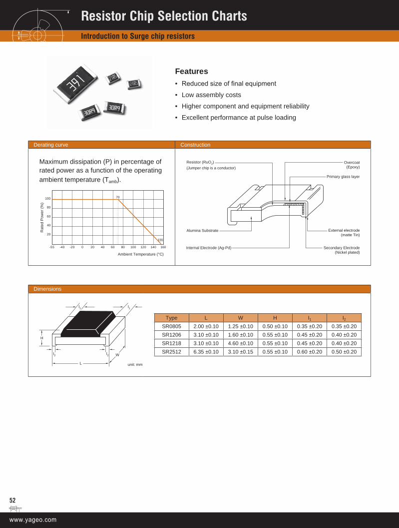
52
FeaturesReduced size of final equipment
Low assembly costs
Higher component and equipment reliability
Excellent performance at pulse loading
•
•
•
•
Derating curve Construction
Maximum dissipation (P) in percentage of rated power as a function of the operating ambient temperature (Tamb).
100
80
60
40
20
-55 -40 -20 0 20 40 60 80
70
100 120 140 160
Ambient Temperature (°C)
Ra
ted
Po
we
r (%
)
155
Overcoat(Epoxy)
Primary glass layer
Secondary Electrode (Nickel plated)
External electrode(matte Tin)
Resistor (RuO2)
(Jumper chip is a conductor)
Alumina Substrate
Internal Electrode (Ag-Pd)
Dimensions
W
unit: mm
I2
I2
I1
I1
L
H
Type L W H I1 I2SR0805 2.00 ±0.10 1.25 ±0.10 0.50 ±0.10 0.35 ±0.20 0.35 ±0.20SR1206 3.10 ±0.10 1.60 ±0.10 0.55 ±0.10 0.45 ±0.20 0.40 ±0.20SR1218 3.10 ±0.10 4.60 ±0.10 0.55 ±0.10 0.45 ±0.20 0.40 ±0.20SR2512 6.35 ±0.10 3.10 ±0.15 0.55 ±0.10 0.60 ±0.20 0.50 ±0.20
Resistor Chip Selection ChartsIntroduction to Surge chip resistors
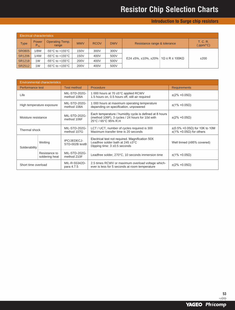
53
Electrical characteristics
Type Power P70
Operating Temp. range MWV RCOV DWV Resistance range & tolerance T. C. R.
( ppm/°C)
SR0805 1/8W -55°C to +155°C 150V 300V 300V
E24 ±5%, ±10%, ±20% 1Ω ≤ R ≤ 100KΩ ±200SR1206 1/4W -55°C to +155°C 150V 400V 500VSR1218 1W -55°C to +155°C 200V 400V 500VSR2512 1W -55°C to +155°C 200V 400V 500V
Environmental characteristics
Performance test Test method Procedure Requirements
Life MIL-STD-202G-method 108A
1 000 hours at 70 ±5°C applied RCWV 1.5 hours on, 0.5 hours off, still air required ±(2% +0.05Ω)
High temperature exposure MIL-STD-202G-method 108A
1 000 hours at maximum operating temperature depending on specification, unpowered ±(1% +0.05Ω)
Moisture resistance MIL-STD-202G-method 106F
Each temperature / humidity cycle is defined at 8 hours (method 106F), 3 cycles / 24 hours for 10d with 25°C / 65°C 95% R.H
±(2% +0.05Ω)
Thermal shock MIL-STD-202G-method 107G
LCT / UCT, number of cycles required is 300 Maximum transfer time is 20 seconds
±(0.5% +0.05Ω) for 10K to 10M ±(1% +0.05Ω) for others
Solderability Wetting IPC/JEDECJ-
STD-002B testB
Electrical test not required. Magnification 50X Leadfree solder bath at 245 ±3°C Dipping time: 3 ±0.5 seconds
Well tinned (≥95% covered)
Resistance to soldering heat
MIL-STD-202G-method 210F Leadfree solder, 270°C, 10 seconds immersion time ±(1% +0.05Ω)
Short time overload MIL-R-55342D-para 4.7.5
2.5 times RCWV or maximum overload voltage which-ever is less for 5 seconds at room temperature ±(2% +0.05Ω)
Resistor Chip Selection ChartsIntroduction to Surge chip resistors
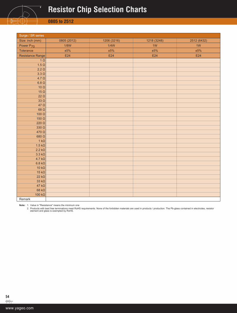
54
Surge / SR seriesSize: inch (mm) 0805 (2012) 1206 (3216) 1218 (3248) 2512 (6432)Power P70 1/8W 1/4W 1W 1WTolerance ±5% ±5% ±5% ±5%Resistance Range E24 E24 E24 E24
1 Ω1.5 Ω2.2 Ω3.3 Ω4.7 Ω6.8 Ω10 Ω15 Ω22 Ω33 Ω47 Ω68 Ω
100 Ω150 Ω220 Ω330 Ω470 Ω680 Ω
1 kΩ1.5 kΩ2.2 kΩ3.3 kΩ4.7 kΩ6.8 kΩ10 kΩ15 kΩ22 kΩ33 kΩ47 kΩ68 kΩ
100 kΩRemark
Note: 1. Value in "Resistance" means the minimum one2. Products with lead free terminations meet RoHS requirements. None of the forbidden materials are used in products / production. The Pb-glass contained in electrodes, resistor
element and glass is exempted by RoHS.
Resistor Chip Selection Charts0805 to 2512
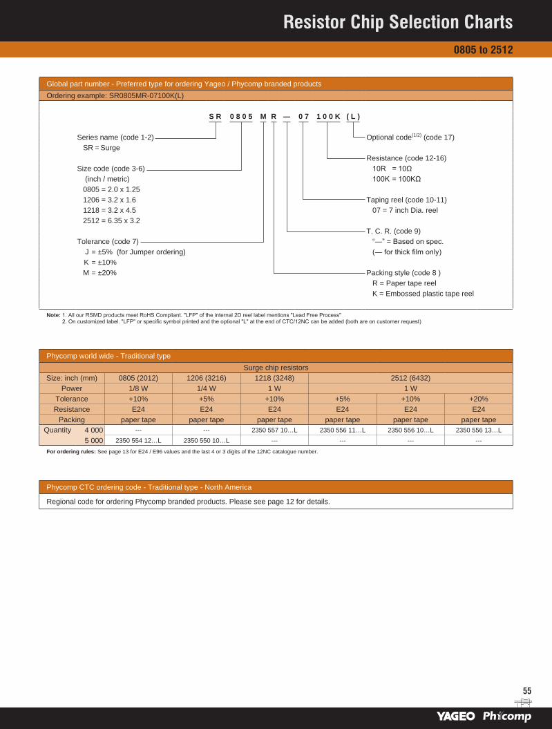
55
Global part number - Preferred type for ordering Yageo / Phycomp branded productsOrdering example: SR0805MR-07100K(L)
S R 0 8 0 5 M R ― 0 7 1 0 0 K ( L )
Series name (code 1-2) Optional code(1/2) (code 17) SR = Surge
Resistance (code 12-16)Size code (code 3-6) 10R = 10Ω
(inch / metric) 100K = 100KΩ0805 = 2.0 x 1.251206 = 3.2 x 1.6 Taping reel (code 10-11)1218 = 3.2 x 4.5 07 = 7 inch Dia. reel2512 = 6.35 x 3.2
T. C. R. (code 9)Tolerance (code 7) “―” = Based on spec.
J = ±5% (for Jumper ordering) (― for thick film only) K = ±10% M = ±20% Packing style (code 8 )
R = Paper tape reelK = Embossed plastic tape reel
Note: 1. All our RSMD products meet RoHS Compliant. "LFP" of the internal 2D reel label mentions "Lead Free Process" 2. On customized label. "LFP" or specific symbol printed and the optional "L" at the end of CTC/12NC can be added (both are on customer request)
Phycomp world wide - Traditional typeSurge chip resistors
Size: inch (mm) 0805 (2012) 1206 (3216) 1218 (3248) 2512 (6432)Power 1/8 W 1/4 W 1 W 1 W
Tolerance +10% +5% +10% +5% +10% +20%Resistance E24 E24 E24 E24 E24 E24
Packing paper tape paper tape paper tape paper tape paper tape paper tapeQuantity 4 000 --- --- 2350 557 10…L 2350 556 11…L 2350 556 10…L 2350 556 13…L
5 000 2350 554 12…L 2350 550 10…L --- --- --- ---
For ordering rules: See page 13 for E24 / E96 values and the last 4 or 3 digits of the 12NC catalogue number.
Phycomp CTC ordering code - Traditional type - North America
Regional code for ordering Phycomp branded products. Please see page 12 for details.
Resistor Chip Selection Charts0805 to 2512

56
FeaturesHigher maximum working voltage to RC series
Extremely thin and light
Reliable electrode construction
Compatible with lead containing and lead free soldering processes
Highly stable in auto-placement surface mounting
•
•
•
•
•
Derating curve Construction
Maximum dissipation (P) in percentage of rated power as a function of the operating ambient temperature (Tamb).
100
80
60
40
20
-55 -40 -20 0 20 40 60 80
70
100 120 140 160
Ambient Temperature (°C)
Ra
ted
Po
we
r (%
)
155
Overcoat(Epoxy)
Primary glass layer
Secondary Electrode (Nickel plated)
External electrode(matte Tin)
Resistor (RuO2)
(Jumper chip is a conductor)
Alumina Substrate
Internal Electrode (Ag-Pd)
Dimensions
W
unit: mm
I2
I2
I1
I1
L
H
Type L W H I1 I2RV0805 2.00 ±0.10 1.25 ±0.10 0.50 ±0.10 0.35 ±0.20 0.35 ±0.20RV1206 3.10 ±0.10 1.60 ±0.10 0.55 ±0.10 0.40 ±0.20 0.40 ±0.20RV2512 6.35 ±0.10 3.10 ±0.15 0.55 ±0.10 0.60 ±0.20 0.50 ±0.20
Resistor Chip Selection ChartsIntroduction to high voltage chip resistors
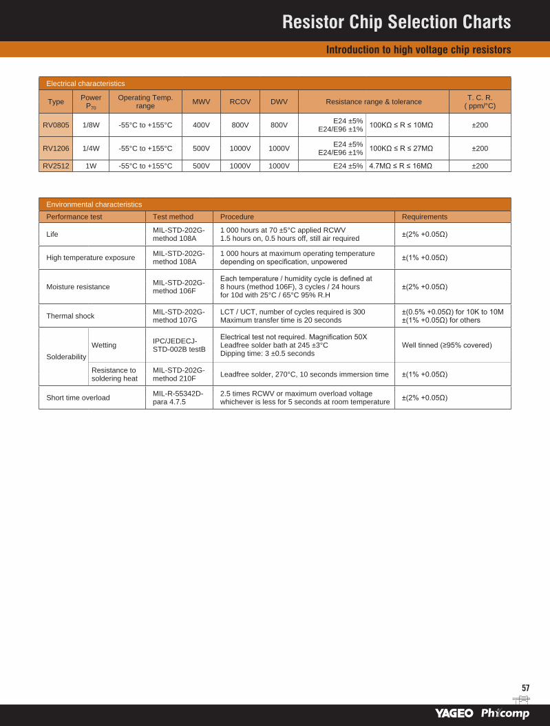
57
Electrical characteristics
Type Power P70
Operating Temp. range MWV RCOV DWV Resistance range & tolerance T. C. R.
( ppm/°C)
RV0805 1/8W -55°C to +155°C 400V 800V 800V E24 ±5% E24/E96 ±1% 100KΩ ≤ R ≤ 10MΩ ±200
RV1206 1/4W -55°C to +155°C 500V 1000V 1000V E24 ±5% E24/E96 ±1% 100KΩ ≤ R ≤ 27MΩ ±200
RV2512 1W -55°C to +155°C 500V 1000V 1000V E24 ±5% 4.7MΩ ≤ R ≤ 16MΩ ±200
Environmental characteristics
Performance test Test method Procedure Requirements
Life MIL-STD-202G-method 108A
1 000 hours at 70 ±5°C applied RCWV 1.5 hours on, 0.5 hours off, still air required ±(2% +0.05Ω)
High temperature exposure MIL-STD-202G-method 108A
1 000 hours at maximum operating temperature depending on specification, unpowered ±(1% +0.05Ω)
Moisture resistance MIL-STD-202G-method 106F
Each temperature / humidity cycle is defined at 8 hours (method 106F), 3 cycles / 24 hours for 10d with 25°C / 65°C 95% R.H
±(2% +0.05Ω)
Thermal shock MIL-STD-202G-method 107G
LCT / UCT, number of cycles required is 300 Maximum transfer time is 20 seconds
±(0.5% +0.05Ω) for 10K to 10M ±(1% +0.05Ω) for others
Solderability Wetting IPC/JEDECJ-
STD-002B testB
Electrical test not required. Magnification 50X Leadfree solder bath at 245 ±3°C Dipping time: 3 ±0.5 seconds
Well tinned (≥95% covered)
Resistance to soldering heat
MIL-STD-202G-method 210F Leadfree solder, 270°C, 10 seconds immersion time ±(1% +0.05Ω)
Short time overload MIL-R-55342D-para 4.7.5
2.5 times RCWV or maximum overload voltage whichever is less for 5 seconds at room temperature ±(2% +0.05Ω)
Resistor Chip Selection ChartsIntroduction to high voltage chip resistors
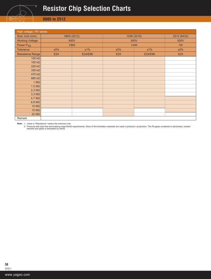
58
High voltage / RV seriesSize: inch (mm) 0805 (2012) 1206 (3216) 2512 (6432)Working Voltage 400V 500V 500VPower P70 1/8W 1/4W 1WTolerance ±5% ±1% ±5% ±1% ±5%Resistance Range E24 E24/E96 E24 E24/E96 E24
100 kΩ150 kΩ220 kΩ330 kΩ470 kΩ680 kΩ
1 MΩ1.5 MΩ2.2 MΩ3.3 MΩ4.7 MΩ6.8 MΩ10 MΩ15 MΩ22 MΩ
Remark
Note: 1. Value in "Resistance" means the minimum one2. Products with lead free terminations meet RoHS requirements. None of the forbidden materials are used in products / production. The Pb-glass contained in electrodes, resistor
element and glass is exempted by RoHS.
Resistor Chip Selection Charts0805 to 2512

59
Global part number - Preferred type for ordering Yageo / Phycomp branded productsOrdering example: RV0805JR-07100K(L)
R V 0 8 0 5 J R ― 0 7 1 0 0 K ( L )
Series name (code 1-2) Optional code(1/2) (code 17) RV = High voltage
Resistance (code 12-16)Size code (code 3-6) 100K = 100KΩ
(inch / metric) 1M = 1MΩ0805 = 2.0 x 1.251206 = 3.2 x 1.6 Taping reel (code 10-11)2512 = 6.35 x 3.2 07 = 7 inch Dia. reel
Tolerance (code 7) T. C. R. (code 9) F = ±1% “―” = Based on spec. J = ±5% (for Jumper ordering) (― for thick film only)
Packing style (code 8 )R = Paper tape reelK = Embossed plastic tape reel
Note: 1. All our RSMD products meet RoHS Compliant. "LFP" of the internal 2D reel label mentions "Lead Free Process" 2. On customized label. "LFP" or specific symbol printed and the optional "L" at the end of CTC/12NC can be added (both are on customer request)
Phycomp world wide - Traditional typeHigh voltage chip resistors
Size: inch (mm) 0805 (2012) 1206 (3216) 2512 (6432)Power 1/8 W 1/4 W 1 W
Tolerance +5% +1% +5% +1% +5%Resistance E24 E24 / E96 E24 E24 / E96 E24
Packing paper tape paper tape blister tapeQuantity 4 000 --- --- --- --- 2322 762 98...L
5 000 2322 792 61...L 2322 793 6....L 2322 790 61...L 2322 791 6....L ---
For ordering rules: See page 13 for E24 / E96 values and the last 4 or 3 digits of the 12NC catalogue number.
Phycomp CTC ordering code - Traditional type - North America
Regional code for ordering Phycomp branded products. Please see page 12 for details.
Resistor Chip Selection Charts0805 to 2512

60
FeaturesReduced size of final equipment
Low assembly costs
Higher component and equipment reliability
Improved performance at high frequency
Low noise, when not trimmed
•
•
•
•
•
Derating curve Construction
Maximum dissipation (P) in percentage of rated power as a function of the operating ambient temperature (Tamb).
100
80
60
40
20
-55 -40 -20 0 20 40 60 80
70
100 120 140 160
Ambient Temperature (°C)
Ra
ted
Po
we
r (%
)
155
TR0805-TR1206
125
TR0402-TR0603
Primary glass layer
Secondary Electrode (Nickel plated)
External electrode(matte Tin)
Resistor (RuO2)
(Jumper chip is a conductor)
Alumina Substrate
Internal Electrode (Ag-Pd)
Dimensions
W
unit: mm
I2
I2
I1
I1
L
H
Type L W H I1 I2TR0402 1.00 ±0.10 0.50 ±0.05 0.35 ±0.05 0.20 ±0.10 0.25 ±0.10TR0603 1.60 ±0.10 0.80 ±0.10 0.45 ±0.10 0.25 ±0.15 0.25 ±0.15TR0805 2.00 ±0.10 1.25 ±0.10 0.50 ±0.10 0.35 ±0.20 0.35 ±0.20TR1206 3.10 ±0.10 1.60 ±0.10 0.55 ±0.10 0.45 ±0.20 0.40 ±0.20
Resistor Chip Selection ChartsIntroduction to trimmable chip resistors

61
Electrical characteristics
Type Power P70
Operating Temp. range MWV RCOV DWV Resistance range & tolerance T. C. R.
( ppm/°C)
TR0402 1/16W -55°C to +125°C 50V 100V 100V
E24 +0/-10%, +0/-20%, +0/-30% 1Ω ≤ R ≤ 10MΩ10Ω < R ≤ 1MΩ ±100
TR0603 1/16W -55°C to +125°C 50V 100V 100VTR0805 1/8W -55°C to +155°C 150V 300V 500V 1Ω ≤ R ≤ 10Ω
1MΩ < R ≤ 10MΩ ±200TR1206 1/4W -55°C to +155°C 200V 500V 500V
Environmental characteristics
Performance test Test method Procedure Requirements
Life MIL-STD-202G-method 108A
1 000 hours at 70 ±5°C applied RCWV 1.5 hours on, 0.5 hours off, still air required ±(2% +0.05Ω)
High temperature exposure MIL-STD-202G-method 108A
1 000 hours at maximum operating temperature depending on specification, unpowered ±(1% +0.05Ω)
Moisture resistance MIL-STD-202G-method 106F
Each temperature / humidity cycle is defined at 8 hours (method 106F), 3 cycles / 24 hours for 10d with 25°C / 65°C 95% R.H
±(2% +0.05Ω)
Thermal shock MIL-STD-202G-method 107G
LCT / UCT, number of cycles required is 300 Maximum transfer time is 20 seconds
±(0.5% +0.05Ω) for 10K to 10M ±(1% +0.05Ω) for others
Solderability Wetting IPC/JEDECJ-
STD-002B testB
Electrical test not required. Magnification 50X Leadfree solder bath at 245 ±3°C Dipping time: 3 ±0.5 seconds
Well tinned (≥95% covered)
Resistance to soldering heat
MIL-STD-202G-method 210F Leadfree solder, 270°C, 10 seconds immersion time ±(1% +0.05Ω)
Short time overload MIL-R-55342D-para 4.7.5
2.5 times RCWV or maximum overload voltage whichever is less for 5 seconds at room temperature ±(2% +0.05Ω)
Resistor Chip Selection ChartsIntroduction to trimmable chip resistors
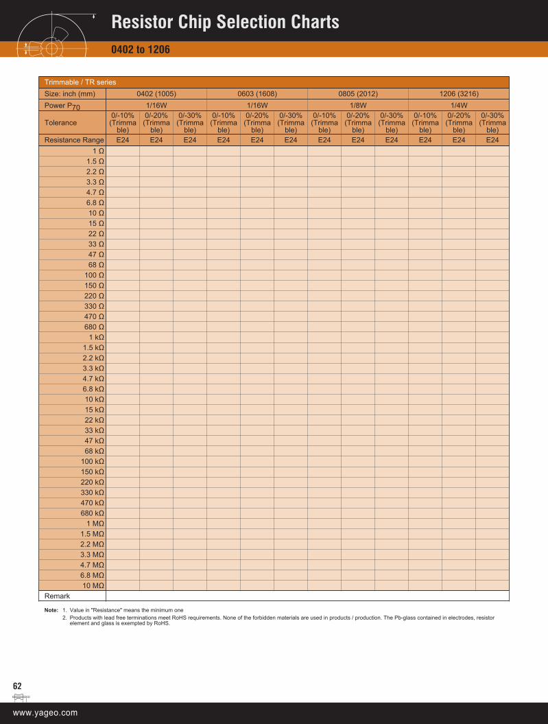
62
Trimmable / TR seriesSize: inch (mm) 0402 (1005) 0603 (1608) 0805 (2012) 1206 (3216)Power P70 1/16W 1/16W 1/8W 1/4W
Tolerance0/-10%(Trimma
ble)
0/-20%(Trimma
ble)
0/-30%(Trimma
ble)
0/-10%(Trimma
ble)
0/-20%(Trimma
ble)
0/-30%(Trimma
ble)
0/-10%(Trimma
ble)
0/-20%(Trimma
ble)
0/-30%(Trimma
ble)
0/-10%(Trimma
ble)
0/-20%(Trimma
ble)
0/-30%(Trimma
ble)Resistance Range E24 E24 E24 E24 E24 E24 E24 E24 E24 E24 E24 E24
1 Ω1.5 Ω2.2 Ω3.3 Ω4.7 Ω6.8 Ω10 Ω15 Ω22 Ω33 Ω47 Ω68 Ω
100 Ω150 Ω220 Ω330 Ω470 Ω680 Ω
1 kΩ1.5 kΩ2.2 kΩ3.3 kΩ4.7 kΩ6.8 kΩ10 kΩ15 kΩ22 kΩ33 kΩ47 kΩ68 kΩ
100 kΩ150 kΩ220 kΩ330 kΩ470 kΩ680 kΩ
1 MΩ1.5 MΩ2.2 MΩ3.3 MΩ4.7 MΩ6.8 MΩ10 MΩ
Remark
Note: 1. Value in "Resistance" means the minimum one2. Products with lead free terminations meet RoHS requirements. None of the forbidden materials are used in products / production. The Pb-glass contained in electrodes, resistor
element and glass is exempted by RoHS.
Resistor Chip Selection Charts0402 to 1206
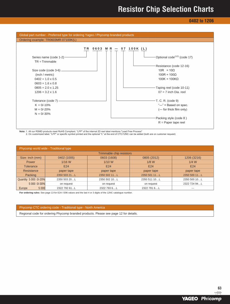
63
Global part number - Preferred type for ordering Yageo / Phycomp branded productsOrdering example: TR0603MR-07100K(L)
T R 0 6 0 3 M R ― 0 7 1 0 0 K ( L )
Series name (code 1-2) Optional code(1/2) (code 17) TR = Trimmable
Resistance (code 12-16)Size code (code 3-6) 10R = 10Ω
(inch / metric) 100R = 100Ω0402 = 1.0 x 0.5 100K = 100KΩ0603 = 1.6 x 0.80805 = 2.0 x 1.25 Taping reel (code 10-11)1206 = 3.2 x 1.6 07 = 7 inch Dia. reel
Tolerance (code 7) T. C. R. (code 9) K = 0/-10% “―” = Based on spec. M = 0/-20% (― for thick film only) N = 0/-30%
Packing style (code 8 )R = Paper tape reel
Note: 1. All our RSMD products meet RoHS Compliant. "LFP" of the internal 2D reel label mentions "Lead Free Process" 2. On customized label. "LFP" or specific symbol printed and the optional "L" at the end of CTC/12NC can be added (both are on customer request)
Phycomp world wide - Traditional typeTrimmable chip resistors
Size: inch (mm) 0402 (1005) 0603 (1608) 0805 (2012) 1206 (3216)Power 1/16 W 1/10 W 1/8 W 1/4 W
Tolerance E24 E24 E24 E24Resistance paper tape paper tape paper tape paper tape
Packing 2350 503 21…L 2350 502 11…L 2350 501 11…L 2350 500 11…L
Quantity 5 000 0/-20% 2350 503 20…L 2350 502 10…L 2350 511 10…L 2350 500 10…L
5 000 0/-30% on request on request on request 2322 724 94…L
Europe 5 000 2322 792 61...L 2322 793 6....L 2322 791 6....L ---
For ordering rules: See page 13 for E24 / E96 values and the last 4 or 3 digits of the 12NC catalogue number.
Phycomp CTC ordering code - Traditional type - North America
Regional code for ordering Phycomp branded products. Please see page 12 for details.
Resistor Chip Selection Charts0402 to 1206

64
FeaturesExcellent TCR compare to thick film low ohmic
Precision current sensing control
Excellent performance for current sensing applicatIons
Ultra low ohmic down to 0.001Ω
•
•
•
•
Derating curve Construction
Maximum dissipation (P) in percentage of rated power as a function of the operating ambient temperature (Tamb).
100
80
60
40
20
-55 -40 -20 0 20 40 60 80
70
100 120 140 160
Ambient Temperature (°C)
Ra
ted
Po
we
r (%
)
155
PR2010PR2512PF2512PT1218PT2512
125
PT0402 to PT1206PT2010
H
PF / PT seriesPR series
W R005
I2
protective coat
marking
end termination
L
I1
end termination
metal substrate
protective coat
protective coat
W
L
I1
protective coat
resistive layer
inner electrode
termination
ceramic substrate
H
I2
Construction will be adjusted to resistance value
Dimensions
PR seriyttsType Resistance range L W H l1 l2
PR2010 2 mΩ - 6 mΩ 5.10 ±0.20 2.50 ±0.20 0.55 ±0.20 0.75 ±0.20 0.75 ±0.20
PR25121 mΩ - 2 mΩ 6.30 ±0.20 3.20 ±0.20 0.75 ±0.15 1.20 ±0.20 1.20 ±0.203 mΩ - 5 mΩ 6.30 ±0.20 3.20 ±0.20 0.55 ±0.15 0.60 ±0.20 0.60 ±0.20
Note: For relevant physical dimensions, please refer to above construction outlines
PF seriesType Resistance range L W H l1 l2
PF25126 mΩ - 14 mΩ
6.50 ±0.25 3.15 ±0.25 0.60 ±0.25 1.00 ±0.251.75 ±0.25
15 mΩ - 130 mΩ 0.60 ±0.25Note: For relevant physical dimensions, please refer to above construction outlines Please contact with sales offices, distributors and representatives in your region before order
PT seriesType Resistance range L W H l1 l2
PT0402
100 mΩ - 910 mΩ
1.00 ±0.10 0.50 ±0.05 0.35 ±0.05 0.20 ±0.10 0.25 ±0.10PT0603 1.60 ±0.10 0.80 ±0.10 0.45 ±0.10 0.25 ±0.15 0.25 ±0.15PT0805 2.00 ±0.10 1.25 ±0.10 0.50 ±0.10 0.35 ±0.20 0.35 ±0.20PT1206 3.10 ±0.10 1.60 ±0.10 0.55 ±0.10 0.45 ±0.20 0.45 ±0.20PT1210 3.10 ±0.10 2.60 ±0.15 0.50 ±0.10 0.50 ±0.20 0.50 ±0.20PT1218 3.05 ±0.15 4.60 ±0.10 0.55 ±0.10 0.45 ±0.25 0.50 ±0.25PT2010 5.00 ±0.10 2.50 ±0.15 0.55 ±0.10 0.60 ±0.20 0.50 ±0.20PT2512 6.35 ±0.10 3.20 ±0.15 0.55 ±0.10 0.60 ±0.20 0.50 ±0.20
Note: For relevant physical dimensions, please refer to above construction outlines Please contact with sales offices, distributors and representatives in your region before order
Resistor Chip Selection ChartsIntroduction to current sensors - low TCR chip resistors
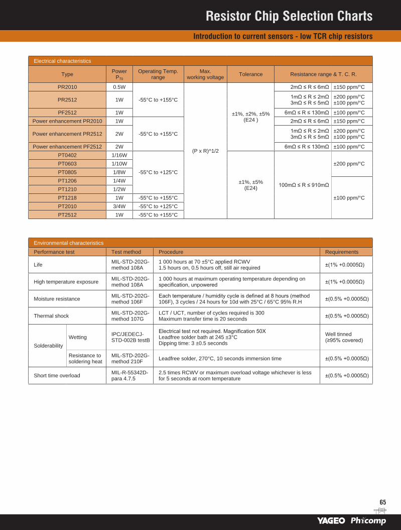
65
Electrical characteristics
Type Power P70
Operating Temp. range
Max. working voltage Tolerance Resistance range & T. C. R.
PR2010 0.5W
-55°C to +155°C
(P x R)^1/2
±1%, ±2%, ±5% (E24 )
2mΩ ≤ R ≤ 6mΩ ±150 ppm/°C
PR2512 1W 1mΩ ≤ R ≤ 2mΩ3mΩ ≤ R ≤ 5mΩ
±200 ppm/°C ±100 ppm/°C
PF2512 1W 6mΩ ≤ R ≤ 130mΩ ±100 ppm/°CPower enhancement PR2010 1W
-55°C to +155°C
2mΩ ≤ R ≤ 6mΩ ±150 ppm/°C
Power enhancement PR2512 2W 1mΩ ≤ R ≤ 2mΩ3mΩ ≤ R ≤ 5mΩ
±200 ppm/°C ±100 ppm/°C
Power enhancement PF2512 2W 6mΩ ≤ R ≤ 130mΩ ±100 ppm/°CPT0402 1/16W
-55°C to +125°C
±1%, ±5% (E24) 100mΩ ≤ R ≤ 910mΩ
±200 ppm/°CPT0603 1/10WPT0805 1/8WPT1206 1/4W
±100 ppm/°CPT1210 1/2WPT1218 1W -55°C to +155°CPT2010 3/4W -55°C to +125°CPT2512 1W -55°C to +155°C
Environmental characteristics
Performance test Test method Procedure Requirements
Life MIL-STD-202G-method 108A
1 000 hours at 70 ±5°C applied RCWV 1.5 hours on, 0.5 hours off, still air required ±(1% +0.0005Ω)
High temperature exposure MIL-STD-202G-method 108A
1 000 hours at maximum operating temperature depending on specification, unpowered ±(1% +0.0005Ω)
Moisture resistance MIL-STD-202G-method 106F
Each temperature / humidity cycle is defined at 8 hours (method 106F), 3 cycles / 24 hours for 10d with 25°C / 65°C 95% R.H ±(0.5% +0.0005Ω)
Thermal shock MIL-STD-202G-method 107G
LCT / UCT, number of cycles required is 300 Maximum transfer time is 20 seconds ±(0.5% +0.0005Ω)
Solderability Wetting IPC/JEDECJ-
STD-002B testB
Electrical test not required. Magnification 50X Leadfree solder bath at 245 ±3°C Dipping time: 3 ±0.5 seconds
Well tinned (≥95% covered)
Resistance to soldering heat
MIL-STD-202G-method 210F Leadfree solder, 270°C, 10 seconds immersion time ±(0.5% +0.0005Ω)
Short time overload MIL-R-55342D-para 4.7.5
2.5 times RCWV or maximum overload voltage whichever is less for 5 seconds at room temperature ±(0.5% +0.0005Ω)
Resistor Chip Selection ChartsIntroduction to current sensors - low TCR chip resistors
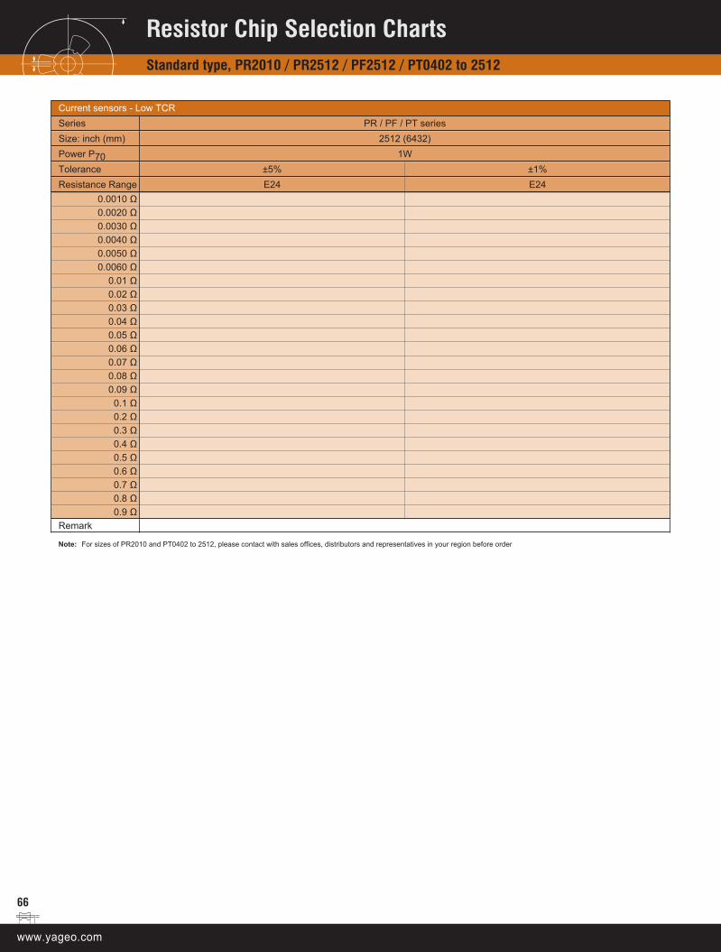
66
Current sensors - Low TCRSeries PR / PF / PT seriesSize: inch (mm) 2512 (6432)Power P70 1WTolerance ±5% ±1%Resistance Range E24 E24
0.0010 Ω0.0020 Ω0.0030 Ω0.0040 Ω0.0050 Ω0.0060 Ω
0.01 Ω0.02 Ω0.03 Ω0.04 Ω0.05 Ω0.06 Ω0.07 Ω0.08 Ω0.09 Ω
0.1 Ω0.2 Ω0.3 Ω0.4 Ω0.5 Ω0.6 Ω0.7 Ω0.8 Ω0.9 Ω
Remark
Note: For sizes of PR2010 and PT0402 to 2512, please contact with sales offices, distributors and representatives in your region before order
Resistor Chip Selection ChartsStandard type, PR2010 / PR2512 / PF2512 / PT0402 to 2512
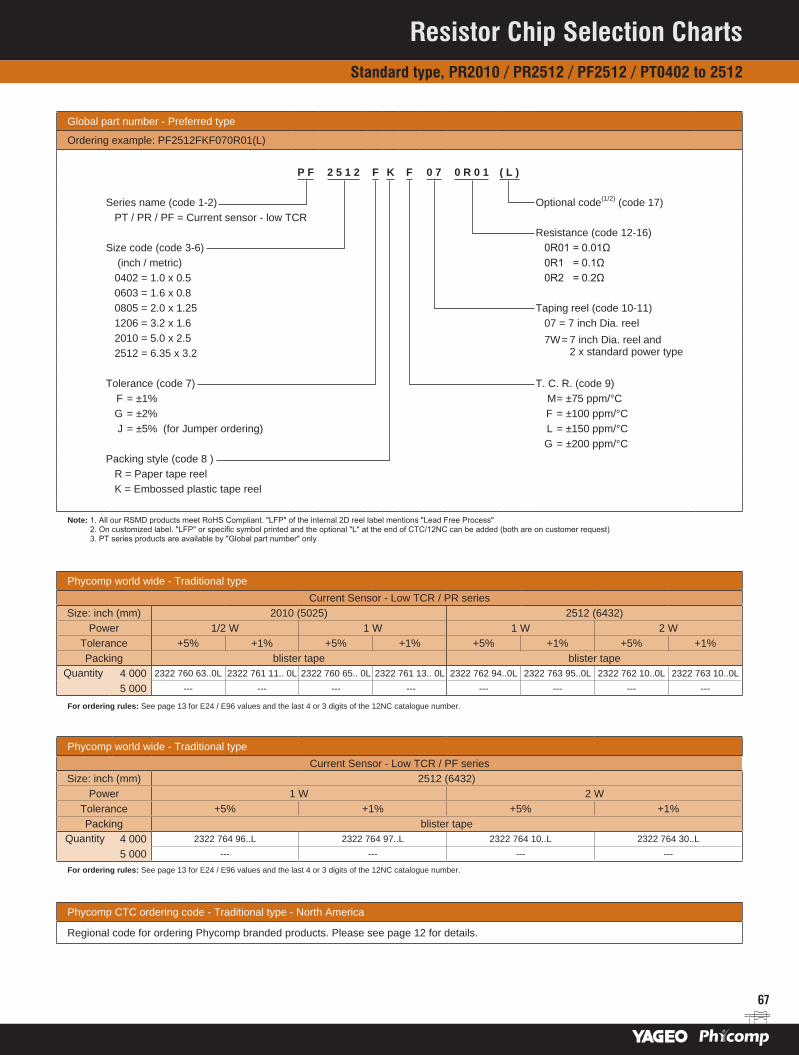
67
Global part number - Preferred type
Ordering example: PF2512FKF070R01(L)
P F 2 5 1 2 F K F 0 7 0 R 0 1 ( L )
Series name (code 1-2) Optional code(1/2) (code 17)PT / PR / PF = Current sensor - low TCR Resistance (code 12-16)
Size code (code 3-6) 0R01 = 0.01Ω (inch / metric) 0R1 = 0.1Ω0402 = 1.0 x 0.5 0R2 = 0.2Ω0603 = 1.6 x 0.80805 = 2.0 x 1.25 Taping reel (code 10-11)1206 = 3.2 x 1.6 07 = 7 inch Dia. reel2010 = 5.0 x 2.5 7W = 7 inch Dia. reel and
2 x standard power type2512 = 6.35 x 3.2
Tolerance (code 7) T. C. R. (code 9) F = ±1% M = ±75 ppm/°C G = ±2% F = ±100 ppm/°C J = ±5% (for Jumper ordering) L = ±150 ppm/°C
G = ±200 ppm/°CPacking style (code 8 )
R = Paper tape reelK = Embossed plastic tape reel
Note: 1. All our RSMD products meet RoHS Compliant. "LFP" of the internal 2D reel label mentions "Lead Free Process" 2. On customized label. "LFP" or specific symbol printed and the optional "L" at the end of CTC/12NC can be added (both are on customer request) 3. PT series products are available by "Global part number" only
Phycomp world wide - Traditional typeCurrent Sensor - Low TCR / PR series
Size: inch (mm) 2010 (5025) 2512 (6432)Power 1/2 W 1 W 1 W 2 W
Tolerance +5% +1% +5% +1% +5% +1% +5% +1%Packing blister tape blister tape
Quantity 4 000 2322 760 63..0L 2322 761 11.. 0L 2322 760 65.. 0L 2322 761 13.. 0L 2322 762 94..0L 2322 763 95..0L 2322 762 10..0L 2322 763 10..0L
5 000 --- --- --- --- --- --- --- ---
For ordering rules: See page 13 for E24 / E96 values and the last 4 or 3 digits of the 12NC catalogue number.
Phycomp world wide - Traditional typeCurrent Sensor - Low TCR / PF series
Size: inch (mm) 2512 (6432)Power 1 W 2 W
Tolerance +5% +1% +5% +1%Packing blister tape
Quantity 4 000 2322 764 96..L 2322 764 97..L 2322 764 10..L 2322 764 30..L
5 000 --- --- --- ---
For ordering rules: See page 13 for E24 / E96 values and the last 4 or 3 digits of the 12NC catalogue number.
Phycomp CTC ordering code - Traditional type - North America
Regional code for ordering Phycomp branded products. Please see page 12 for details.
Resistor Chip Selection ChartsStandard type, PR2010 / PR2512 / PF2512 / PT0402 to 2512

68
FeaturesMobile phone
Receivers
Battery charger
Palmtop computers
PDAs
•
•
•
•
•
Derating curve Construction Schematics
Maximum dissipation (P) in percent-age of rated power as a function of the operating ambient temperature (Tamb).
100
80
60
40
20
-55 -40 -20 0 20 40 60 80
70
100 120 140 160
Ambient Temperature (°C)
Ra
ted
Po
we
r (%
)
125
1 3
2 4
input signalattenuated output signal
The rectangular marker designates input pin 1
1 3
R2R2
R1
2 4
ATV 321
Dimensions
L
P
B
W
T
D
A
unit: mm
Type L W T A B P D
ATV321 1.00 ±0.10 1.00 ±0.10 0.35 ±0.05 0.33 ±0.10 0.15 ±0.10 0.65 ±0.10 0.25 ±0.10
Resistor Chip Selection ChartsIntroduction to RF attenuator chip resistors
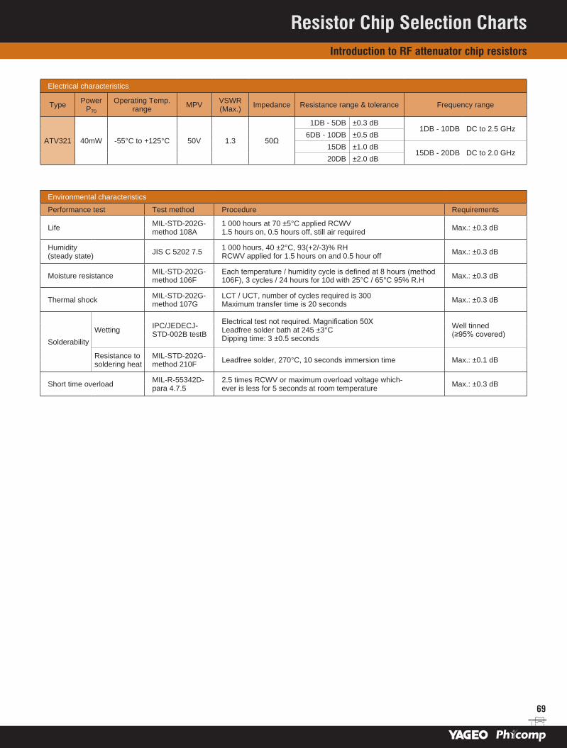
69
Electrical characteristics
Type Power P70
Operating Temp. range MPV VSWR
(Max.) Impedance Resistance range & tolerance Frequency range
ATV321 40mW -55°C to +125°C 50V 1.3 50Ω
1DB - 5DB ±0.3 dB1DB - 10DB DC to 2.5 GHz
6DB - 10DB ±0.5 dB15DB ±1.0 dB
15DB - 20DB DC to 2.0 GHz 20DB ±2.0 dB
Environmental characteristics
Performance test Test method Procedure Requirements
Life MIL-STD-202G-method 108A
1 000 hours at 70 ±5°C applied RCWV 1.5 hours on, 0.5 hours off, still air required Max.: ±0.3 dB
Humidity (steady state) JIS C 5202 7.5 1 000 hours, 40 ±2°C, 93(+2/-3)% RH
RCWV applied for 1.5 hours on and 0.5 hour off Max.: ±0.3 dB
Moisture resistance MIL-STD-202G-method 106F
Each temperature / humidity cycle is defined at 8 hours (method 106F), 3 cycles / 24 hours for 10d with 25°C / 65°C 95% R.H Max.: ±0.3 dB
Thermal shock MIL-STD-202G-method 107G
LCT / UCT, number of cycles required is 300 Maximum transfer time is 20 seconds Max.: ±0.3 dB
Solderability Wetting IPC/JEDECJ-
STD-002B testB
Electrical test not required. Magnification 50X Leadfree solder bath at 245 ±3°C Dipping time: 3 ±0.5 seconds
Well tinned (≥95% covered)
Resistance to soldering heat
MIL-STD-202G-method 210F Leadfree solder, 270°C, 10 seconds immersion time Max.: ±0.1 dB
Short time overload MIL-R-55342D-para 4.7.5
2.5 times RCWV or maximum overload voltage which-ever is less for 5 seconds at room temperature Max.: ±0.3 dB
Resistor Chip Selection ChartsIntroduction to RF attenuator chip resistors
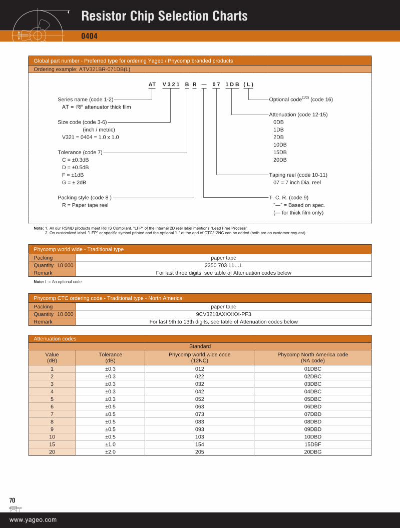
70
Global part number - Preferred type for ordering Yageo / Phycomp branded productsOrdering example: ATV321BR-071DB(L)
AT V 3 2 1 B R ― 0 7 1 D B ( L )
Series name (code 1-2) Optional code(1/2) (code 16)AT = RF attenuator thick film
Attenuation (code 12-15)Size code (code 3-6) 0DB
(inch / metric) 1DBV321 = 0404 = 1.0 x 1.0 2DB
10DBTolerance (code 7) 15DB
C = ±0.3dB 20DBD = ±0.5dBF = ±1dB Taping reel (code 10-11)G = ± 2dB 07 = 7 inch Dia. reel
Packing style (code 8 ) T. C. R. (code 9)R = Paper tape reel “―” = Based on spec.
(― for thick film only)
Note: 1. All our RSMD products meet RoHS Compliant. "LFP" of the internal 2D reel label mentions "Lead Free Process" 2. On customized label. "LFP" or specific symbol printed and the optional "L" at the end of CTC/12NC can be added (both are on customer request)
Phycomp world wide - Traditional typePacking paper tapeQuantity 10 000 2350 703 11…L Remark For last three digits, see table of Attenuation codes belowNote: L = An optional code
Phycomp CTC ordering code - Traditional type - North AmericaPacking paper tapeQuantity 10 000 9CV3218AXXXXX-PF3Remark For last 9th to 13th digits, see table of Attenuation codes below
Attenuation codesStandard
Value (dB)
Tolerance (dB)
Phycomp world wide code (12NC)
Phycomp North America code (NA code)
1 ±0.3 012 01DBC2 ±0.3 022 02DBC3 ±0.3 032 03DBC4 ±0.3 042 04DBC5 ±0.3 052 05DBC6 ±0.5 063 06DBD7 ±0.5 073 07DBD8 ±0.5 083 08DBD9 ±0.5 093 09DBD
10 ±0.5 103 10DBD15 ±1.0 154 15DBF20 ±2.0 205 20DBG
Resistor Chip Selection Charts0404
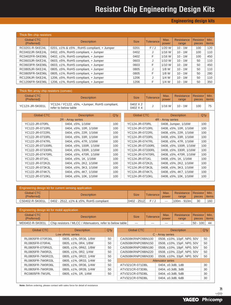
71
Thick film chip resistorsGlobal CTC (Preferred) Description Size Tolerance Max.
powerResistance
rangeResistor pieces
Min. items
RC0201-R-SKE24L 0201, ±1% & ±5% , RoHS compliant, + Jumper 0201 F / J 1/20 W 10 - 1M 100 120RC0402JR-SKE24L 0402, ±5%, RoHS compliant, + Jumper 0402 J 1/16 W 10 - 1M 100 110RC0402FR-SKE96L 0402, ±1%, RoHS compliant, + Jumper 0402 F 1/16 W 10 - 1M 100 450RC0603JR-SKE24L 0603, ±5%, RoHS compliant, + Jumper 0603 J 1/10 W 10 - 1M 50 110RC0603FR-SKE96L 0603, ±1%, RoHS compliant, + Jumper 0603 F 1/10 W 10 - 1M 50 450RC0805JR-SKE24L 0805, ±5%, RoHS compliant, + Jumper 0805 J 1/8 W 10 - 1M 50 110RC0805FR-SKE96L 0805, ±1%, RoHS compliant, + Jumper 0805 F 1/8 W 10 - 1M 50 280RC1206JR-SKE24L 1206, ±5%, RoHS compliant, + Jumper 1206 J 1/4 W 10 - 1M 50 110RC1206FR-SKE96L 1206, ±1%, RoHS compliant, + Jumper 1206 F 1/4 W 10 - 1M 50 350
Thick film array chip resistors (convex)Global CTC (Preferred) Description Size Tolerance Max.
powerResistance
rangeResistor pieces
Min. items
YC12X-JR-SK001L YC124 / YC122, ±5%, +Jumper, RoHS compliant, refer to below table
0402 X 2 0402 X 4 J 1/16 W 10 - 1M 100 75
Global CTC Description Q’ty Global CTC Description Q’ty2R - Array series 4R - Array series
YC122-JR-070RL 0404, ±5%, 1/16W 100 YC124-JR-070RL 0408, Jumper, 1/16W 100YC122-JR-0710RL 0404, ±5%, 10R, 1/16W 100 YC124-JR-0710RL 0408, ±5%, 10R, 1/16W 100YC122-JR-0722RL 0404, ±5%, 22R, 1/16W 100 YC124-JR-0722RL 0408, ±5%, 22R, 1/16W 100YC122-JR-0733RL 0404, ±5%, 33R, 1/16W 100 YC124-JR-0733RL 0408, ±5%, 33R, 1/16W 100YC122-JR-0747RL 0404, ±5%, 47R, 1/16W 100 YC124-JR-0747RL 0408, ±5%, 47R, 1/16W 100YC122-JR-07100RL 0404, ±5%, 100R, 1/16W 100 YC124-JR-07100RL 0408, ±5%, 100R, 1/16W 100YC122-JR-07330RL 0404, ±5%, 330R, 1/16W 100 YC124-JR-07330RL 0408, ±5%, 330R, 1/16W 100YC122-JR-07470RL 0404, ±5%, 470R, 1/16W 100 YC124-JR-07470RL 0408, ±5%, 470R, 1/16W 100YC122-JR-071KL 0404, ±5%, 1K, 1/16W 100 YC124-JR-071KL 0408, ±5%, 1K, 1/16W 100YC122-JR-072K2L 0404, ±5%, 2K2, 1/16W 100 YC124-JR-072K2L 0408, ±5%, 2K2, 1/16W 100YC122-JR-073K3L 0404, ±5%, 3K3, 1/16W 100 YC124-JR-073K3L 0408, ±5%, 3K3, 1/16W 100YC122-JR-074K7L 0404, ±5%, 4K7, 1/16W 100 YC124-JR-074K7L 0408, ±5%, 4K7, 1/16W 100YC122-JR-0710KL 0404, ±5%, 10K, 1/16W 100 YC124-JR-0710KL 0408, ±5%, 10K, 1/16W 100
Engineering design kit for current sensing applicationGlobal CTC (Preferred) Description Size Tolerance Max.
powerResistance
rangeResistor pieces
Min. items
CS0402-R-SK001L 0402 - 2512, ±1% & ±5%, RoHS compliant 0402 - 2512 F / J --- 100m - 910m 30 160
Engineering design kit for mobil applicationGlobal CTC (Preferred) Description Size Tolerance Max.
powerResistance
rangeResistor pieces
Min. items
MD0402-R-SK001L Chip resistors / MLCC / Attenuators, refer to below table --- --- --- --- 50 - 100 44
Global CTC Description Q’ty Global CTC Description Q’tyLow ohmic series C - Array series
RL0805FR-070R36L 0805, ±1%, 0R36, 1/8W 50 CA0508KRNPO9BN100 0508, ±10%, 10pF, NP0, 50V 50RL0805FR-070R4L 0805, ±1%, 0R4, 1/8W 50 CA0508KRNPO9BN150 0508, ±10%, 15pF, NP0, 50V 50RL0805FR-070R62L 0805, ±1%, 0R62, 1/8W 50 CA0508KRNPO9BN180 0508, ±10%, 18pF, NP0, 50V 50RL0805FR-7W0R2L 0805, ±1%, 0R2, 1/4W 50 CA0508KRNPO9BN220 0508, ±10%, 22pF, NP0, 50V 50RL0805FR-7W0R22L 0805, ±1%, 0R22, 1/4W 50 CA0508KRNPO9BN330 0508, ±10%, 33pF, NP0, 50V 50RL0805FR-7W0R33L 0805, ±1%, 0R33, 1/4W 50 Attenuiator seriesRL0805FR-7W0R36L 0805, ±1%, 0R36, 1/4W 50 ATV321CR-071DBL 0404, ±0.3dB, 1dB 30RL0805FR-7W0R39L 0805, ±1%, 0R39, 1/4W 50 ATV321CR-073DBL 0404, ±0.3dB, 3dB 30RC0805FR-7W1RL 0805, ±1%, 1R, 1/4W 50 ATV321CR-075DBL 0404, ±0.3dB, 5dB 30
ATV321CR-076DBL 0404, ±0.3dB, 6dB 30
Note: Before ordering, please contact with sales force for detail of resistance
Resistor Chip Engineering Design KitsEngineering design kits

SMD CERAMIC MILTILAYER CAPACITORS

74
Specification overview
Description TC code Series Capacitance range Voltage range Size
Discrete
NP0
General purpose 0.22 pF to 33 nF 16 V to 25 V 0201, 0402, 0603, 0805, 1206, 1210
General purpose 0.22 pF to 390 pF 50 V0201, 0402, 0603, 0805, 1206, 1210, 1812
Medium voltage 10 pF to 22 nF 100 V to 630 V 0603, 0805, 1206, 1210, 1808, 1812
High voltage 10 pF to 2.7 nF1 kV, 2 kV, 3 kV, 4 kV
1206, 1210, 1808, 1812
Microwave 0.47 pF to 120 pF 50 V 0603, 0805, 1206
X7R
General purpose & High capacitance 100 pF to 22 µF 6.3 V to 50 V0201, 0402, 0603, 0805, 1206, 1210, 1812
Medium voltage 100 pF to 470 nF 100 V to 630 V 0603, 0805, 1206, 1210, 1808, 1812
High voltage 100 pF to 33 nF 1 kV to 3 kV 1206, 1210, 1808, 1812
Low inductance 10 nF to 220 nF 10 V to 50 V 0306, 0508, 0612
X5R General purpose & High capacitance 10 nF to 100 µF 6.3 V to 50 V0201, 0402, 0603, 0805, 1206, 1210, 1812
Y5V General purpose & High capacitance 10 nF to 47 µF 6.3 V to 50 V 0201, 0402, 0603, 0805, 1206, 1210
Safety certification product
NP0 High voltage SC type 10 pF to 1 nF X1/Y2, X2/Y3 1808, 1812
X7R High voltage SC type 150 pF to 1.5 nF X1/Y2, X2/Y3 1808, 1812
C-Arrays
NP0 4-C arrays 10 pF to 1 nF 50 V 0508, 0612
X7R2-C arrays 10 nF to 100 nF 16 V 0405
4-C arrays 220 pF to 100 nF 16 V to 50 V 0508, 0612
Y5V 4-C arrays 10 nF to 100 nF 25 V 0508, 0612
High frequency NP0 High frequency 0.22 pF to 10 pF 50 V 0402, 0603
MLCC General InformationSpecification overview

75
Case dimensions
Discrete capacitors
L2 L3L4
L1
W
Case size designation Dimensions in mm
Inch-based Metric L1 W L2 / L3 min L2 / L3 max L4 min
0201 0603M 0.6 ±0.03 0.3 ±0.03 0.10 0.20 0.20
0402 1005M 1.0 ±0.05 0.5 ±0.05 0.20 0.30 0.40
0603 1608M 1.6 ±0.10 0.8 ±0.07 0.20 0.60 0.40
0805 2012M 2.0 ±0.10 1.25 ±0.10 0.25 0.75 0.55
1206 3216M 3.2 ±0.15 1.6 ±0.15 0.25 0.75 1.40
1210 3225M 3.2 ±0.20 2.5 ±0.20 0.25 0.75 1.40
1808 4520M 4.5 ±0.40 2.0 ±0.30 0.25 0.75 2.20
1812 4532M 4.5 ±0.20 3.2 ±0.20 0.25 0.75 2.20
Discrete capacitors - High voltage SC type /
L2 L3L4
L1
W
Case size designation Dimensions in mm
Inch-based Metric L1 W L2 / L3 min L2 / L3 max L4 min
1808 4520M 4.8 ±0.30 2.0 ±0.30 0.25 0.75 3.20
1812 4532M 4.8 ±0.30 3.2 ±0.30 0.25 0.75 4.00
2-C arrays
T
WF
A
B
PL
Case size designation Demensions in mm
Inch-based Metric L W Tmin Tmax A B P
0405 (2 x 0402)
1013M(2 x 1005) 1.37 ±0.15 1.0 ±0.15 0.5 0.7 0.36 ±0.1 0.2 ±0.1 0.64 ±0.1
4-C arrays
L
PA
T
B
W
Case size designation Dimensions in mm
Inch-based Metric L W Tmin Tmax A B P
0508 (4 x 0402)
1220M (4 x 1005) 2.0 ±0.15 1.25 ±0.15 0.50 0.70 0.28 ±0.10 0.2 ±0.10 0.5 ±0.10
0612 (4 x 0603)
1632M (4 x 1608) 3.2 ±0.15 1.60 ±0.15 0.70 0.90 0.4 ±0.10 0.3 ±0.20 0.8 ±0.10
Discrete capacitors - Low inductance types only
T
L2 L3L4
L1
W
Case size designation Dimensions in mm
Inch-based Metric L1 W T L2 / L3 min L2 / L3 max L4 min
0306 0816M 0.8 ±0.15 1.6 ±0.20 0.50 ±0.10 0.10 0.30 0.20
0508 1220M 1.25 ±0.20 2.0 ±0.20 0.85 ±0.10 0.13 0.46 0.38
0612 1632M 1.6 ±0.20 3.2 ±0.20 0.85 ±0.10 0.13 0.46 0.50
MLCC General InformationCase dimensions
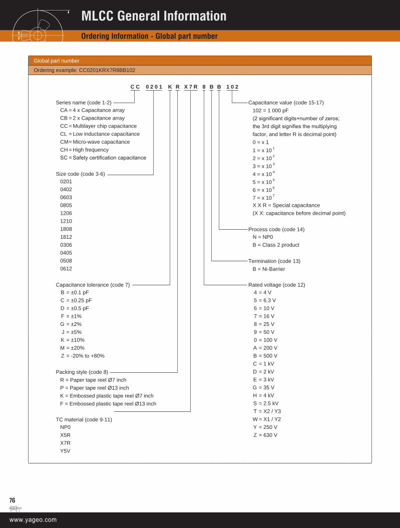
76
Global part number
Ordering example: CC0201KRX7R8BB102
C C 0 2 0 1 K R X 7 R 8 B B 1 0 2
Series name (code 1-2) Capacitance value (code 15-17) CA = 4 x Capacitance array 102 = 1 000 pF CB = 2 x Capacitance array (2 significant digits+number of zeros; CC = Multilayer chip capacitance the 3rd digit signifies the multiplying CL = Low inductance capacitance factor, and letter R is decimal point) CM = Micro-wave capacitance 0 = x 1 CH = High frequency 1 = x 10 1
SC = Safety certification capacitance 2 = x 10 2
3 = x 10 3
Size code (code 3-6) 4 = x 10 4
0201 5 = x 10 5
0402 6 = x 10 6
0603 7 = x 10 7
0805 X X R = Special capacitance1206 (X X: capacitance before decimal point) 12101808 Process code (code 14)1812 N = NP00306 B = Class 2 product04050508 Termination (code 13)0612 B = Ni-Barrier
Capacitance tolerance (code 7) Rated voltage (code 12) B = ±0.1 pF 4 = 4 V C = ±0.25 pF 5 = 6.3 V D = ±0.5 pF 6 = 10 V F = ±1% 7 = 16 V G = ±2% 8 = 25 V J = ±5% 9 = 50 V K = ±10% 0 = 100 V M = ±20% A = 200 V Z = -20% to +80% B = 500 V C = 1 kV
Packing style (code 8) D = 2 kVR = Paper tape reel Ø7 inch E = 3 kVP = Paper tape reel Ø13 inch G = 35 VK = Embossed plastic tape reel Ø7 inch H = 4 kVF = Embossed plastic tape reel Ø13 inch S = 2.5 kV
T = X2 / Y3 TC material (code 9-11) W = X1 / Y2
NP0 Y = 250 VX5R Z = 630 VX7RY5V
MLCC General InformationOrdering Information - Global part number
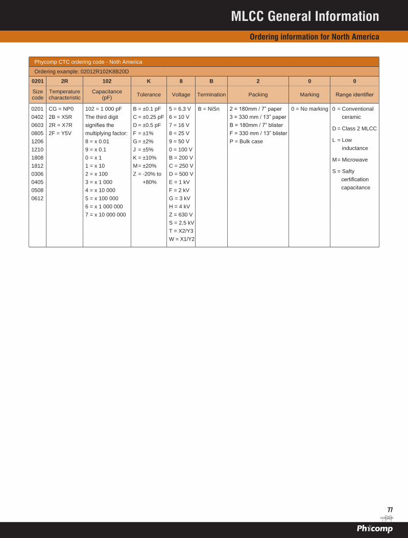
77
Phycomp CTC ordering code - Noth America
Ordering example: 02012R102K8B20D
0201 2R 102 K 8 B 2 0 0
Size code
Temperature characteristic
Capacitance (pF) Tolerance Voltage Termination Packing Marking Range identifier
0201 0402 0603 0805 1206 1210 1808 1812 03060405 0508 0612
CG = NP0 2B = X5R 2R = X7R 2F = Y5V
102 = 1 000 pF The third digit signifies the multiplying factor: 8 = x 0.01 9 = x 0.1 0 = x 1 1 = x 10 2 = x 100 3 = x 1 000 4 = x 10 000 5 = x 100 000 6 = x 1 000 000 7 = x 10 000 000
B = ±0.1 pF C = ±0.25 pF D = ±0.5 pF F = ±1% G = ±2% J = ±5% K = ±10% M = ±20% Z = -20% to +80%
5 = 6.3 V 6 = 10 V 7 = 16 V 8 = 25 V 9 = 50 V 0 = 100 V B = 200 V C = 250 V D = 500 V E = 1 kV F = 2 kV G = 3 kV H = 4 kVZ = 630 VS = 2.5 kVT = X2/Y3W = X1/Y2
B = NiSn 2 = 180mm / 7” paper 3 = 330 mm / 13” paper B = 180mm / 7” blister F = 330 mm / 13” blister P = Bulk case
0 = No marking 0 = Conventional ceramic
D = Class 2 MLCC
L = Low inductance
M = Microwave
S = Safty certification capacitance
MLCC General InformationOrdering information for North America

78
Thickness classes and packing quantities
Description Size code
Thickness classification
(mm)
Quantity per reel Quantity per
bulk caseTape width 180 mm / 7” 330 mm / 13”
Paper Blister Paper Blister
Discrete capacitors
0201 0.3 ±0.03
8 mm
15 000 --- 50 000 --- ---
0402 0.5 ±0.05 10 000 --- 50 000 --- 50 000
0603 0.8 ±0.1 4 000 --- 15 000 --- 15 000
0805
0.6 ±0.1 4 000 --- 20 000 --- 10 000
0.85 ±0.1 4 000 --- 15 000 --- 8 000
1.25 ±0.2 --- 3 000 --- 10 000 5 000
1206
0.6 ±0.1 4 000 --- 20 000 --- ---
0.85 ±0.1 4 000 --- 15 000 --- ---
1.00 / 1.15 ±0.1 --- 3 000 --- 10 000 ---
1.25 ±0.2 --- 3 000 --- 10 000 ---
1.6 ±0.15 --- 2 500 --- 10 000 ---
1.6 ±0.2 --- 2 000 --- 10 000 ---
1210
0.6 / 0.7 ±0.1 --- 4 000 --- 15 000 ---
0.85 ±0.1 --- 4 000 --- 10 000 ---
1.15 ±0.1 --- 3 000 --- 10 000 ---
1.15 ±0.15 --- 3 000 --- 10 000 ---
1.25 ±0.2 --- 3 000 --- --- ---
1.5 ±0.1 --- 2 000 --- --- ---
1.6 / 1.9 ±0.2 --- 2 000 --- --- ---
2.0 ±0.2 --- 2 000 / 1 000 --- --- ---
2.5 ±0.2 --- 1 000 / 500 --- --- ---
1808
1.15 ±0.15
12 mm
--- 3 000 --- --- ---
1.25 ±0.2 --- 3 000 --- --- ---
1.35 ±0.15 --- 2 000 --- --- ---
1.5 ±0.1 --- 2 000 --- --- ---
1.6 ±0.2 --- 2 000 --- --- ---
2.0 ±0.2 --- 2 000 --- --- ---
1812
0.6 / 0.85 ±0.1 --- 2 000 --- --- ---
1.15 ±0.1 --- 1 500 --- --- ---
1.15 ±0.15 --- 1 500 --- --- ---
1.35 ±0.15 --- 1 000 --- --- ---
1.5 ±0.1 --- 1 000 --- --- ---
1.6 ±0.2 --- 1 000 --- --- ---
2.0 ±0.2 --- 1 000 --- --- ---
Low inductance
0306 0.5 ±0.1
8 mm
4 000 --- 15 000 --- ---
0508 0.85 ±0.1 4 000 --- 15 000 --- ---
0612 0.85 ±0.1 4 000 --- 15 000 --- ---
Arrays
0405 0.6 ±0.1 4 000 --- --- --- ---
0508 0.6 ±0.1 4 000 --- --- --- ---
0612 0.8 ±0.1 4 000 --- --- --- ---
MLCC General InformationThickness classes and packing quantities for all series

79
NP0General purpose
Capacitance Last 2-digit of12NC
0201 0402 060325V 16V 25V 16V 25V
10 pF 23 0.5 ±0.0512 pF 2415 pF 2518 pF 2622 pF 2727 pF 28 0.3 ±0.0333 pF 2939 pF 3147 pF 3256 pF 3368 pF 3482 pF 35
100 pF 36120 pF 37150 pF 38180 pF 39220 pF 41270 pF 42 0.5 ±0.05330 pF 43390 pF 44470 pF 45 0.8 ±0.1560 pF 46680 pF 47820 pF 48
1000 pF 491.2 nF 511.5 nF 521.8 nF 53 0.8 ±0.12.2 nF 542.7 nF 553.3 nF 56
Tape width 8 mm
Note: Values in shaded cells indicate thickness class (unit: mm)
MLCC Selection ChartsNP0 - General purpose 16 to 25V, 0201 to 0603
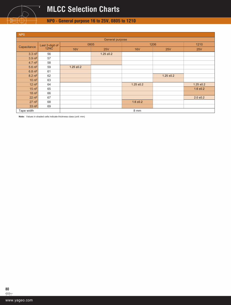
80
NP0General purpose
Capacitance Last 2-digit of12NC
0805 1206 121016V 25V 16V 25V 25V
3.3 nF 56 1.25 ±0.23.9 nF 574.7 nF 585.6 nF 59 1.25 ±0.26.8 nF 618.2 nF 62 1.25 ±0.210 nF 6312 nF 64 1.25 ±0.2 1.25 ±0.215 nF 65 1.6 ±0.218 nF 6622 nF 67 2.0 ±0.227 nF 68 1.6 ±0.233 nF 69
Tape width 8 mm
Note: Values in shaded cells indicate thickness class (unit: mm)
MLCC Selection ChartsNP0 - General purpose 16 to 25V, 0805 to 1210
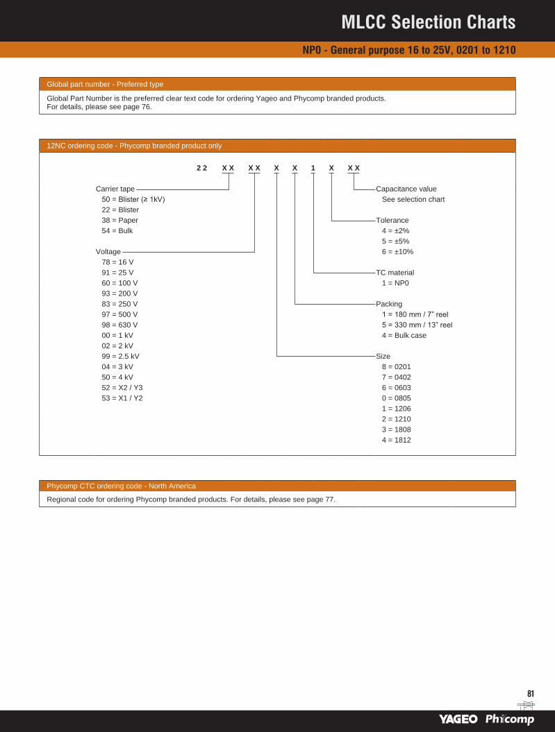
81
Global part number - Preferred type
Global Part Number is the preferred clear text code for ordering Yageo and Phycomp branded products. For details, please see page 76.
12NC ordering code - Phycomp branded product only
2 2 X X X X X X 1 X X X
Carrier tape Capacitance value 50 = Blister (≥ 1kV) See selection chart22 = Blister38 = Paper Tolerance54 = Bulk 4 = ±2%
5 = ±5%Voltage 6 = ±10%
78 = 16 V91 = 25 V TC material60 = 100 V 1 = NP093 = 200 V83 = 250 V Packing97 = 500 V 1 = 180 mm / 7” reel98 = 630 V 5 = 330 mm / 13” reel00 = 1 kV 4 = Bulk case02 = 2 kV99 = 2.5 kV Size04 = 3 kV 8 = 020150 = 4 kV 7 = 040252 = X2 / Y3 6 = 060353 = X1 / Y2 0 = 0805
1 = 12062 = 12103 = 18084 = 1812
Phycomp CTC ordering code - North America
Regional code for ordering Phycomp branded products. For details, please see page 77.
MLCC Selection ChartsNP0 - General purpose 16 to 25V, 0201 to 1210
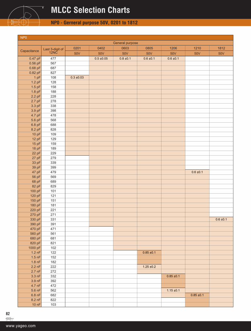
NP0General purpose
Capacitance Last 3-digit of12NC
0201 0402 0603 0805 1206 1210 181250V 50V 50V 50V 50V 50V 50V
0.47 pF 477 0.5 ±0.05 0.8 ±0.1 0.6 ±0.1 0.6 ±0.10.56 pF 5670.68 pF 6870.82 pF 827
1 pF 108 0.3 ±0.031.2 pF 1281.5 pF 1581.8 pF 1882.2 pF 2282.7 pF 2783.3 pF 3383.9 pF 3984.7 pF 4785.6 pF 5686.8 pF 6888.2 pF 82810 pF 10912 pF 12915 pF 15918 pF 18922 pF 22927 pF 27933 pF 33939 pF 39947 pF 479 0.6 ±0.156 pF 56968 pF 68982 pF 829
100 pF 101120 pF 121150 pF 151180 pF 181220 pF 221270 pF 271330 pF 331 0.6 ±0.1390 pF 391470 pF 471560 pF 561680 pF 681820 pF 821
1000 pF 1021.2 nF 122 0.85 ±0.11.5 nF 1521.8 nF 1822.2 nF 222 1.25 ±0.22.7 nF 2723.3 nF 332 0.85 ±0.13.9 nF 3924.7 nF 4725.6 nF 562 1.15 ±0.16.8 nF 682 0.85 ±0.18.2 nF 82210 nF 103
82
MLCC Selection ChartsNP0 - Gerneral purpose 50V, 0201 to 1812
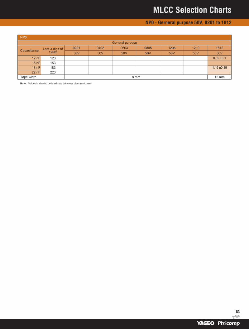
NP0General purpose
Capacitance Last 3-digit of12NC
0201 0402 0603 0805 1206 1210 181250V 50V 50V 50V 50V 50V 50V
12 nF 123 0.85 ±0.115 nF 15318 nF 183 1.15 ±0.1522 nF 223
Tape width 8 mm 12 mm
Note: Values in shaded cells indicate thickness class (unit: mm)
83
MLCC Selection ChartsNP0 - Gerneral purpose 50V, 0201 to 1812

84
Global part number - Preferred type
Global Part Number is the preferred clear text code for ordering Yageo and Phycomp branded products. For details, please see page 76.
12NC ordering code - Phycomp branded product only
2 2 X X X X X X X X X X
Carrier tape Capacitance value 22 = Blister See selection chart38 = Paper54 = Bulk Tolerance
4 = ±0.1 pF for 0.47 pF ≤ C < 5 pF ±0.25 pF for 5 pF ≤ C < 10 pF
Voltage ±2% for C ≥ 10 pF86 = 50 V 5 = ±0.25 pF for C < 5 pF
±0.5 pF for 5 pF ≤ C < 10 pF Size ±5% for C ≥ 10 pF
8 = 0201 8 = ±0.1 pF for 5 pF ≤ C < 10 pF 9 = 0402 ±1% for C ≥ 10 pF7 = 06031 = 0805 Packing3 = 1206 1 = 180 mm / 7” reel2 = 1210 7 = 330 mm / 13” reel5 = 1812 4 = Bulk case
Phycomp CTC ordering code - North America
Regional code for ordering Phycomp branded products. For details, please see page 77.
MLCC Selection ChartsNP0 - Gerneral purpose 50V, 0201 to 1812
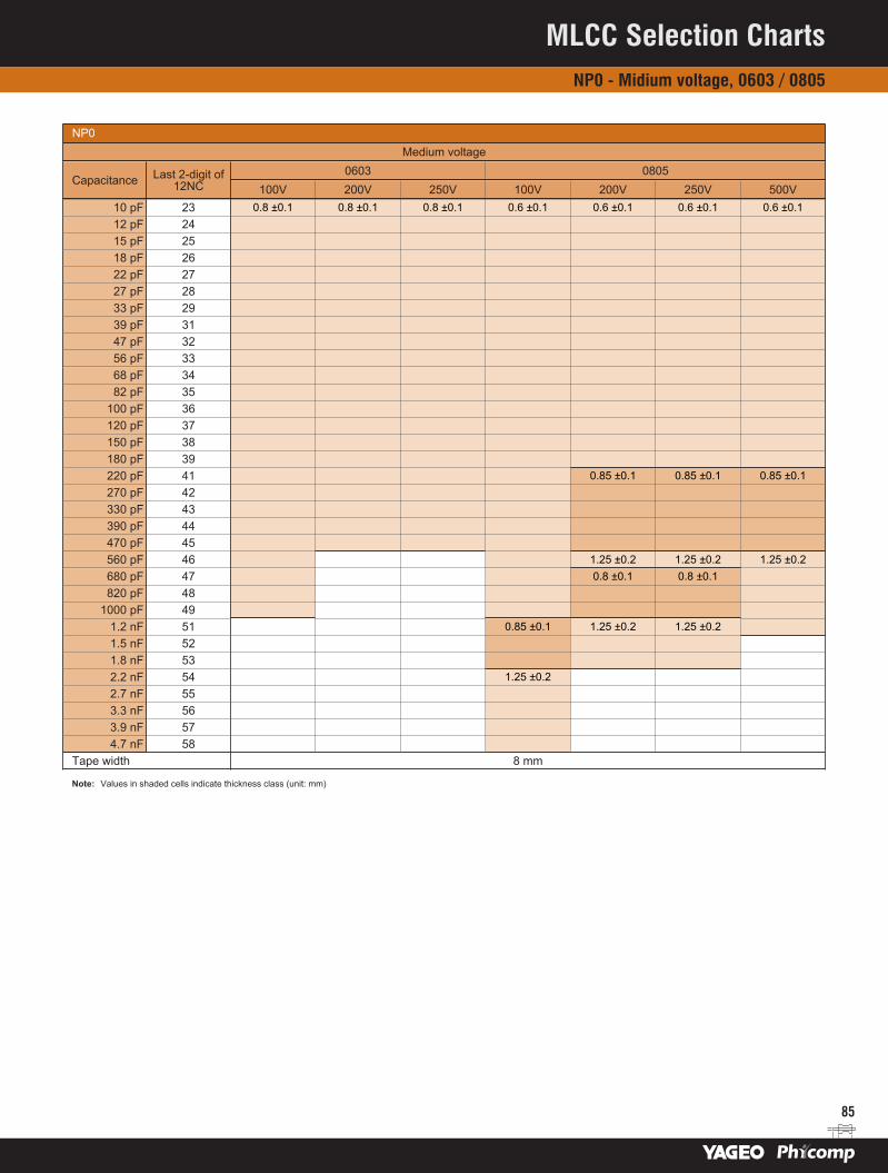
85
NP0Medium voltage
Capacitance Last 2-digit of12NC
0603 0805100V 200V 250V 100V 200V 250V 500V
10 pF 23 0.8 ±0.1 0.8 ±0.1 0.8 ±0.1 0.6 ±0.1 0.6 ±0.1 0.6 ±0.1 0.6 ±0.112 pF 2415 pF 2518 pF 2622 pF 2727 pF 2833 pF 2939 pF 3147 pF 3256 pF 3368 pF 3482 pF 35
100 pF 36120 pF 37150 pF 38180 pF 39220 pF 41 0.85 ±0.1 0.85 ±0.1 0.85 ±0.1270 pF 42330 pF 43390 pF 44470 pF 45560 pF 46 1.25 ±0.2 1.25 ±0.2 1.25 ±0.2680 pF 47 0.8 ±0.1 0.8 ±0.1820 pF 48
1000 pF 491.2 nF 51 0.85 ±0.1 1.25 ±0.2 1.25 ±0.21.5 nF 521.8 nF 532.2 nF 54 1.25 ±0.22.7 nF 553.3 nF 563.9 nF 574.7 nF 58
Tape width 8 mm
Note: Values in shaded cells indicate thickness class (unit: mm)
MLCC Selection ChartsNP0 - Midium voltage, 0603 / 0805
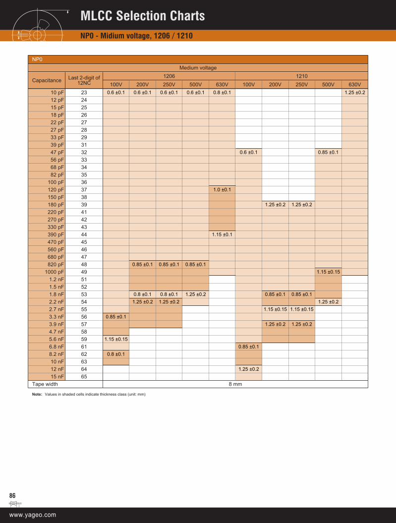
86
NP0Medium voltage
Capacitance Last 2-digit of12NC
1206 1210100V 200V 250V 500V 630V 100V 200V 250V 500V 630V
10 pF 23 0.6 ±0.1 0.6 ±0.1 0.6 ±0.1 0.6 ±0.1 0.8 ±0.1 1.25 ±0.212 pF 2415 pF 2518 pF 2622 pF 2727 pF 2833 pF 2939 pF 3147 pF 32 0.6 ±0.1 0.85 ±0.156 pF 3368 pF 3482 pF 35
100 pF 36120 pF 37 1.0 ±0.1150 pF 38180 pF 39 1.25 ±0.2 1.25 ±0.2220 pF 41270 pF 42330 pF 43390 pF 44 1.15 ±0.1470 pF 45560 pF 46680 pF 47820 pF 48 0.85 ±0.1 0.85 ±0.1 0.85 ±0.1
1000 pF 49 1.15 ±0.151.2 nF 511.5 nF 521.8 nF 53 0.8 ±0.1 0.8 ±0.1 1.25 ±0.2 0.85 ±0.1 0.85 ±0.12.2 nF 54 1.25 ±0.2 1.25 ±0.2 1.25 ±0.22.7 nF 55 1.15 ±0.15 1.15 ±0.153.3 nF 56 0.85 ±0.13.9 nF 57 1.25 ±0.2 1.25 ±0.24.7 nF 585.6 nF 59 1.15 ±0.156.8 nF 61 0.85 ±0.18.2 nF 62 0.8 ±0.110 nF 6312 nF 64 1.25 ±0.215 nF 65
Tape width 8 mm
Note: Values in shaded cells indicate thickness class (unit: mm)
MLCC Selection ChartsNP0 - Midium voltage, 1206 / 1210
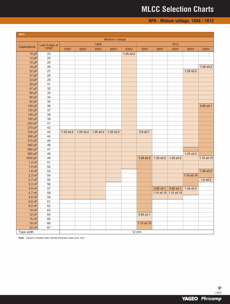
87
NP0Medium voltage
Capacitance Last 2-digit of12NC
1808 1812100V 200V 250V 500V 630V 100V 200V 250V 500V 630V
10 pF 23 1.25 ±0.212 pF 2415 pF 2518 pF 26 1.25 ±0.222 pF 27 1.25 ±0.227 pF 2833 pF 2939 pF 3147 pF 3256 pF 3368 pF 3482 pF 35
100 pF 36 0.85 ±0.1120 pF 37150 pF 38180 pF 39220 pF 41270 pF 42330 pF 43 1.25 ±0.2 1.25 ±0.2 1.25 ±0.2 1.25 ±0.2 0.6 ±0.1390 pF 44470 pF 45560 pF 46680 pF 47820 pF 48 1.25 ±0.2
1000 pF 49 1.25 ±0.2 1.25 ±0.2 1.25 ±0.2 1.15 ±0.151.2 nF 511.5 nF 521.8 nF 53 1.25 ±0.22.2 nF 54 1.15 ±0.152.7 nF 55 1.6 ±0.23.3 nF 563.9 nF 57 0.85 ±0.1 0.85 ±0.1 1.25 ±0.24.7 nF 58 1.15 ±0.15 1.15 ±0.155.6 nF 596.8 nF 618.2 nF 6210 nF 6312 nF 64 0.85 ±0.115 nF 6518 nF 66 1.15 ±0.1522 nF 67
Tape width 12 mm
Note: Values in shaded cells indicate thickness class (unit: mm)
MLCC Selection ChartsNP0 - Midium voltage, 1808 / 1812

88
NP0High voltage
Capacitance Last 2-digit of12NC
1206 12101kV 2kV 1kV 2kV
10 pF 23 0.8 ±0.1 1.0 ±0.1 1.25 ±0.2 1.25 ±0.212 pF 2415 pF 2518 pF 2622 pF 2727 pF 2833 pF 2939 pF 3147 pF 3256 pF 3368 pF 3482 pF 35
100 pF 36120 pF 37 1.0 ±0.1 0.8 ±0.1150 pF 38180 pF 39220 pF 41 1.25 ±0.2270 pF 42330 pF 43390 pF 44 1.15 ±0.15470 pF 45560 pF 46680 pF 47820 pF 48
1000 pF 49Tape width 8 mm
Note: Values in shaded cells indicate thickness class (unit: mm)
MLCC Selection ChartsNP0 - High voltage, 1206 / 1210
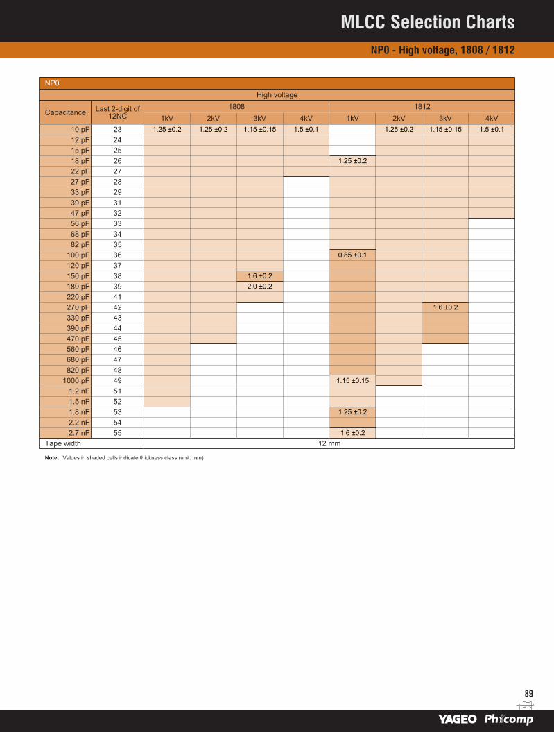
89
NP0High voltage
Capacitance Last 2-digit of12NC
1808 18121kV 2kV 3kV 4kV 1kV 2kV 3kV 4kV
10 pF 23 1.25 ±0.2 1.25 ±0.2 1.15 ±0.15 1.5 ±0.1 1.25 ±0.2 1.15 ±0.15 1.5 ±0.112 pF 2415 pF 2518 pF 26 1.25 ±0.222 pF 2727 pF 2833 pF 2939 pF 3147 pF 3256 pF 3368 pF 3482 pF 35
100 pF 36 0.85 ±0.1120 pF 37150 pF 38 1.6 ±0.2180 pF 39 2.0 ±0.2220 pF 41270 pF 42 1.6 ±0.2330 pF 43390 pF 44470 pF 45560 pF 46680 pF 47820 pF 48
1000 pF 49 1.15 ±0.151.2 nF 511.5 nF 521.8 nF 53 1.25 ±0.22.2 nF 542.7 nF 55 1.6 ±0.2
Tape width 12 mm
Note: Values in shaded cells indicate thickness class (unit: mm)
MLCC Selection ChartsNP0 - High voltage, 1808 / 1812
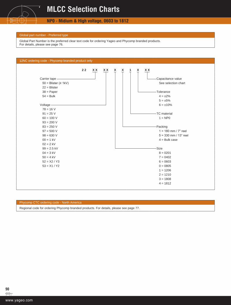
90
Global part number - Preferred type
Global Part Number is the preferred clear text code for ordering Yageo and Phycomp branded products. For details, please see page 76.
12NC ordering code - Phycomp branded product only
2 2 X X X X X X 1 X X X
Carrier tape Capacitance value 50 = Blister (≥ 1kV) See selection chart22 = Blister38 = Paper Tolerance54 = Bulk 4 = ±2%
5 = ±5%Voltage 6 = ±10%
78 = 16 V91 = 25 V TC material60 = 100 V 1 = NP093 = 200 V83 = 250 V Packing97 = 500 V 1 = 180 mm / 7” reel98 = 630 V 5 = 330 mm / 13” reel00 = 1 kV 4 = Bulk case02 = 2 kV99 = 2.5 kV Size04 = 3 kV 8 = 020150 = 4 kV 7 = 040252 = X2 / Y3 6 = 060353 = X1 / Y2 0 = 0805
1 = 12062 = 12103 = 18084 = 1812
Phycomp CTC ordering code - North America
Regional code for ordering Phycomp branded products. For details, please see page 77.
MLCC Selection ChartsNP0 - Midium & High voltage, 0603 to 1812
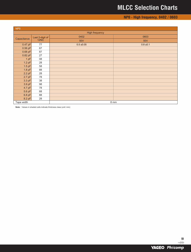
91
NP0High frequency
Capacitance Last 2-digit of12NC
0402 060350V 50V
0.47 pF 77 0.5 ±0.05 0.8 ±0.10.56 pF 670.68 pF 870.82 pF 27
1 pF 081.2 pF 281.5 pF 581.8 pF 882.2 pF 282.7 pF 783.3 pF 383.9 pF 984.7 pF 785.6 pF 686.8 pF 888.2 pF 28
Tape width 8 mm
Note: Values in shaded cells indicate thickness class (unit: mm)
MLCC Selection ChartsNP0 - High frequency, 0402 / 0603

92
Global part number - Preferred type
Global Part Number is the preferred clear text code for ordering Yageo and Phycomp branded products. For details, please see page 76.
12NC ordering code - Phycomp branded product only
2 2 X X X X X X X X X X
Carrier tape Capacitance value 22 = Blister See selection chart38 = Paper54 = Bulk Tolerance
4 = ±0.1 pF for 0.47 pF ≤ C < 5 pF ±0.25 pF for 5 pF ≤ C < 10 pF
Voltage ±2% for C ≥ 10 pF84 = 50 V (for high frequency series) 5 = ±0.25 pF for C < 5 pF
±0.5 pF for 5 pF ≤ C < 10 pF Size ±5% for C ≥ 10 pF
9 = 0402 8 = ±0.1 pF for 5 pF ≤ C < 10 pF 7 = 0603 ±1% for C ≥ 10 pF
Packing1 = 180 mm / 7” reel7 = 330 mm / 13” reel4 = Bulk case
Phycomp CTC ordering code - North America
Regional code for ordering Phycomp branded products. For details, please see page 77.
MLCC Selection ChartsNP0 - High frequency, 0402 / 0603
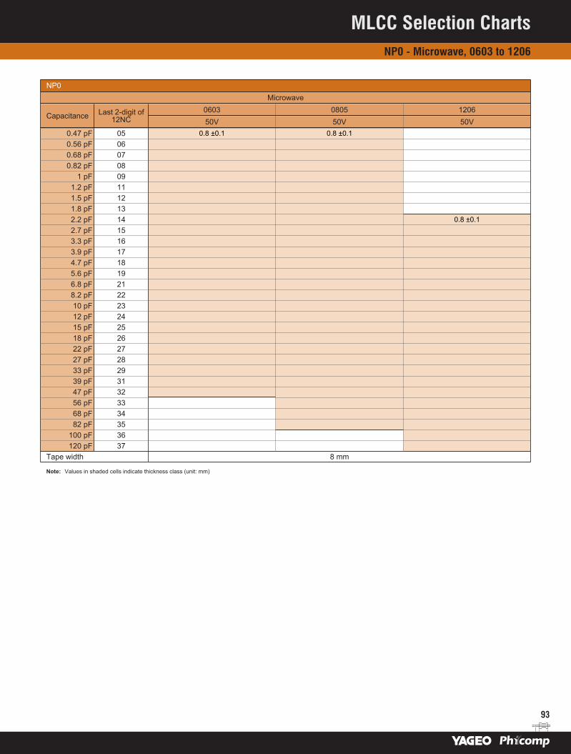
93
NP0Microwave
Capacitance Last 2-digit of12NC
0603 0805 120650V 50V 50V
0.47 pF 05 0.8 ±0.1 0.8 ±0.10.56 pF 060.68 pF 070.82 pF 08
1 pF 091.2 pF 111.5 pF 121.8 pF 132.2 pF 14 0.8 ±0.12.7 pF 153.3 pF 163.9 pF 174.7 pF 185.6 pF 196.8 pF 218.2 pF 2210 pF 2312 pF 2415 pF 2518 pF 2622 pF 2727 pF 2833 pF 2939 pF 3147 pF 3256 pF 3368 pF 3482 pF 35
100 pF 36120 pF 37
Tape width 8 mm
Note: Values in shaded cells indicate thickness class (unit: mm)
MLCC Selection ChartsNP0 - Microwave, 0603 to 1206

94
Global part number - Preferred type
Global Part Number is the preferred clear text code for ordering Yageo and Phycomp branded products. For details, please see page 76.
12NC ordering code - Phycomp branded product only
2 2 X X X X X X 1 X X X
Carrier tape Capacitance value 38 = Paper See selection chart54 = Bulk
ToleranceSize 0 = ±0.1 pF for C < 10 pF
578 = 0603 1 = ±0.25 pF for C < 10 pF 574 = 0805 2 = ±0.5 pF for 5 pF ≤ C < 10 pF 576 = 1206 3 = ±1% for C ≥ 10 pF
4 = ±2% pF for C ≥ 10 pF Packing 5 = ±5% for C ≥ 10 pF
1 = 180 mm / 7” reel5 = 330 mm / 13” reel4 = Bulk case
Phycomp CTC ordering code - North America
Regional code for ordering Phycomp branded products. For details, please see page 77.
MLCC Selection ChartsNP0 - Microwave, 0603 to 1206
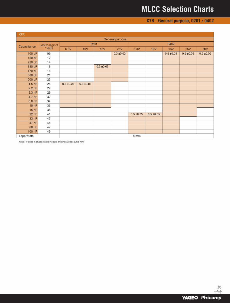
95
X7RGeneral purpose
Capacitance Last 2-digit of12NC
0201 04026.3V 10V 16V 25V 6.3V 10V 16V 25V 50V
100 pF 09 0.3 ±0.03 0.5 ±0.05 0.5 ±0.05 0.5 ±0.05150 pF 12220 pF 14330 pF 16 0.3 ±0.03470 pF 18680 pF 21
1000 pF 231.5 nF 25 0.3 ±0.03 0.3 ±0.032.2 nF 273.3 nF 294.7 nF 326.8 nF 3410 nF 3615 nF 3822 nF 41 0.5 ±0.05 0.5 ±0.0533 nF 4347 nF 4568 nF 47
100 nF 49Tape width 8 mm
Note: Values in shaded cells indicate thickness class (unit: mm)
MLCC Selection ChartsX7R - General purpose, 0201 / 0402

96
X7RGeneral purpose & High capacitance
Capacitance Last 2-digit of12NC
0603 08056.3V 10V 16V 25V 50V 6.3V 10V 16V 25V 50V
100 pF 09 0.8 ±0.1 0.8 ±0.1 0.8 ±0.1 0.8 ±0.1150 pF 12220 pF 14 0.6 ±0.1330 pF 16470 pF 18680 pF 21
1000 pF 231.5 nF 252.2 nF 273.3 nF 294.7 nF 326.8 nF 3410 nF 36 0.6 ±0.115 nF 3822 nF 4133 nF 43 0.85 ±0.147 nF 45 0.6 ±0.1 0.85 ±0.168 nF 47
100 nF 49 0.8 ±0.1 0.85 ±0.1 0.85 ±0.1150 nF 52 0.85 ±0.1220 nF 54 1.25 ±0.2330 nF 56 1.25 ±0.2 1.25 ±0.2 1.25 ±0.2 1.25 ±0.2470 nF 58680 nF 61 1.25 ±0.2
1000 nF 632.2 uF 674.7 uF 7210 uF 76
Tape width 8 mm
Note: Values in shaded cells indicate thickness class (unit: mm)
MLCC Selection ChartsX7R - General purpose & High capacitance, 0603 / 0805
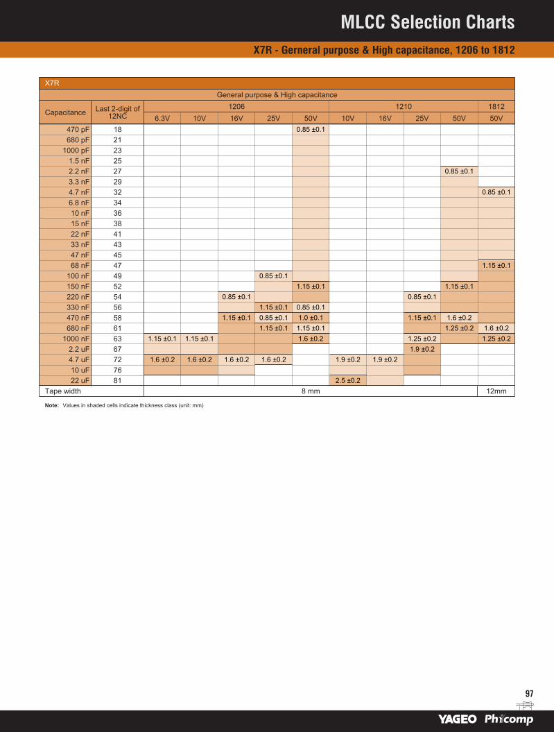
97
X7RGeneral purpose & High capacitance
Capacitance Last 2-digit of12NC
1206 1210 18126.3V 10V 16V 25V 50V 10V 16V 25V 50V 50V
470 pF 18 0.85 ±0.1680 pF 21
1000 pF 231.5 nF 252.2 nF 27 0.85 ±0.13.3 nF 294.7 nF 32 0.85 ±0.16.8 nF 3410 nF 3615 nF 3822 nF 4133 nF 4347 nF 4568 nF 47 1.15 ±0.1
100 nF 49 0.85 ±0.1150 nF 52 1.15 ±0.1 1.15 ±0.1220 nF 54 0.85 ±0.1 0.85 ±0.1330 nF 56 1.15 ±0.1 0.85 ±0.1470 nF 58 1.15 ±0.1 0.85 ±0.1 1.0 ±0.1 1.15 ±0.1 1.6 ±0.2680 nF 61 1.15 ±0.1 1.15 ±0.1 1.25 ±0.2 1.6 ±0.2
1000 nF 63 1.15 ±0.1 1.15 ±0.1 1.6 ±0.2 1.25 ±0.2 1.25 ±0.22.2 uF 67 1.9 ±0.24.7 uF 72 1.6 ±0.2 1.6 ±0.2 1.6 ±0.2 1.6 ±0.2 1.9 ±0.2 1.9 ±0.210 uF 7622 uF 81 2.5 ±0.2
Tape width 8 mm 12mm
Note: Values in shaded cells indicate thickness class (unit: mm)
MLCC Selection ChartsX7R - Gerneral purpose & High capacitance, 1206 to 1812

98
X7RMedium voltage
Capacitance Last 2-digit of12NC
0603 0805100V 100V 200V 250V 500V
100 pF 09 0.8 ±0.1150 pF 12 0.8 ±0.1220 pF 14 0.6 ±0.1 0.85 ±0.1 0.85 ±0.1330 pF 16470 pF 18680 pF 21
1000 pF 231.5 nF 252.2 nF 272.7 nF 283.3 nF 294.7 nF 325.6 nF 336.8 nF 34 1.25 ±0.2 1.25 ±0.210 nF 36 1.25 ±0.215 nF 38 0.85 ±0.1 0.8 ±0.1 0.8 ±0.122 nF 41 1.25 ±0.2 1.25 ±0.233 nF 43 1.25 ±0.247 nF 45
Tape width 8 mm
Note: Values in shaded cells indicate thickness class (unit: mm)
MLCC Selection ChartsX7R - Midium voltage, 0603 / 0805
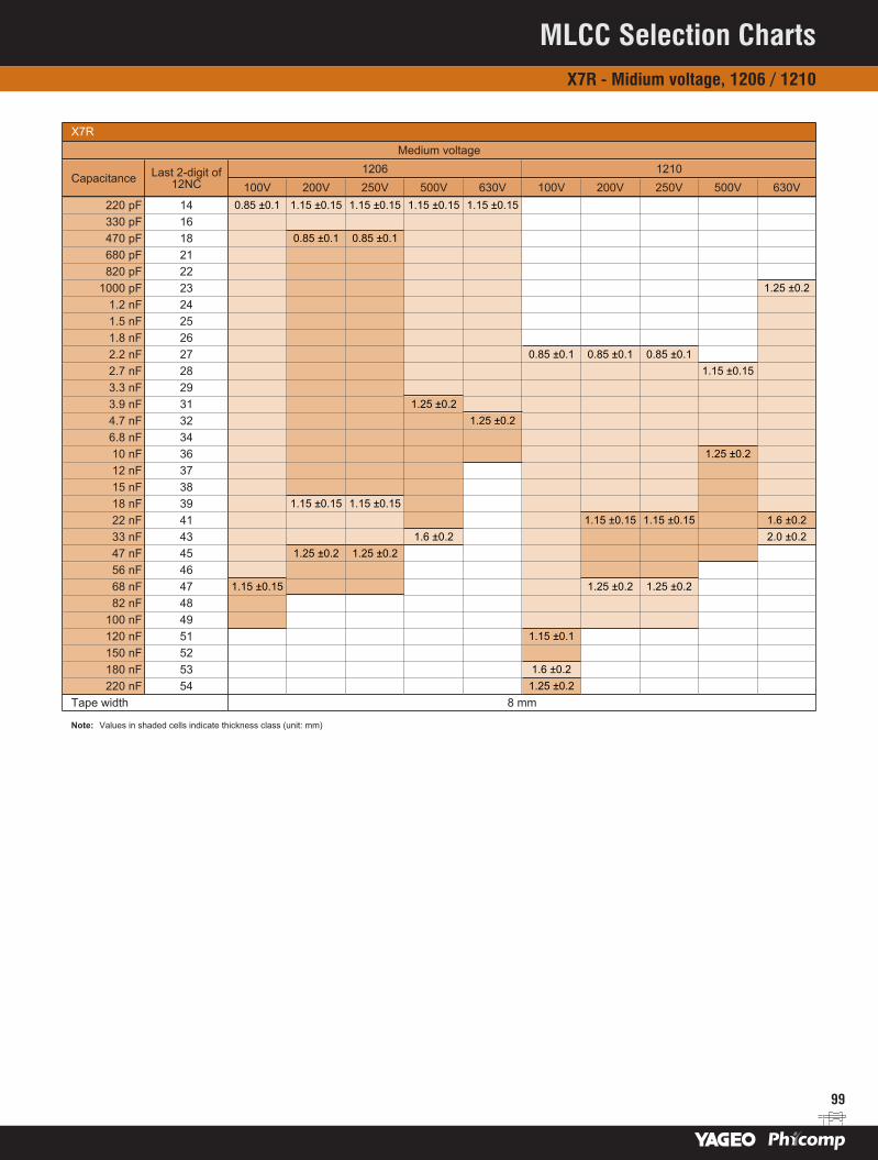
99
X7RMedium voltage
Capacitance Last 2-digit of12NC
1206 1210100V 200V 250V 500V 630V 100V 200V 250V 500V 630V
220 pF 14 0.85 ±0.1 1.15 ±0.15 1.15 ±0.15 1.15 ±0.15 1.15 ±0.15330 pF 16470 pF 18 0.85 ±0.1 0.85 ±0.1680 pF 21820 pF 22
1000 pF 23 1.25 ±0.21.2 nF 241.5 nF 251.8 nF 262.2 nF 27 0.85 ±0.1 0.85 ±0.1 0.85 ±0.12.7 nF 28 1.15 ±0.153.3 nF 293.9 nF 31 1.25 ±0.24.7 nF 32 1.25 ±0.26.8 nF 3410 nF 36 1.25 ±0.212 nF 3715 nF 3818 nF 39 1.15 ±0.15 1.15 ±0.1522 nF 41 1.15 ±0.15 1.15 ±0.15 1.6 ±0.233 nF 43 1.6 ±0.2 2.0 ±0.247 nF 45 1.25 ±0.2 1.25 ±0.256 nF 4668 nF 47 1.15 ±0.15 1.25 ±0.2 1.25 ±0.282 nF 48
100 nF 49120 nF 51 1.15 ±0.1150 nF 52180 nF 53 1.6 ±0.2220 nF 54 1.25 ±0.2
Tape width 8 mm
Note: Values in shaded cells indicate thickness class (unit: mm)
MLCC Selection ChartsX7R - Midium voltage, 1206 / 1210

100
X7RMedium voltage
Capacitance Last 2-digit of12NC
1808 1812100V 200V 250V 500V 630V 100V 200V 250V 500V 630V
1000 pF 23 1.35 ±0.15 1.35 ±0.151.5 nF 262.2 nF 283.3 nF 29 1.25 ±0.2 1.25 ±0.2 1.25 ±0.2 1.25 ±0.2 0.85 ±0.14.7 nF 32 1.25 ±0.2 0.85 ±0.1 0.85 ±0.1 0.85 ±0.16.8 nF 34 1.6 ±0.210 nF 36 1.15 ±0.115 nF 38 1.15 ±0.15 1.25 ±0.222 nF 41 1.25 ±0.233 nF 43 1.6 ±0.247 nF 45 1.15 ±0.15 1.15 ±0.1568 nF 47
100 nF 49 1.15 ±0.1 1.6 ±0.2150 nF 52220 nF 54 1.6 ±0.2 1.6 ±0.2330 nF 56 2.0 ±0.2 2.0 ±0.2470 nF 58 2.0 ±0.2
Tape width 12 mm
Note: Values in shaded cells indicate thickness class (unit: mm)
MLCC Selection ChartsX7R - Midium voltage, 1808 / 1812

101
X7RHigh voltage
Capacitance Last 2-digit of12NC
1206 12101kV 2kV 1kV 2kV
220 pF 14 1.15 ±0.15 1.25 ±0.2330 pF 16470 pF 18680 pF 21
1000 pF 23 1.25 ±0.2 1.25 ±0.21.5 nF 252.2 nF 27 1.6 ±0.23.3 nF 294.7 nF 32 1.25 ±0.26.8 nF 3410 nF 3615 nF 3822 nF 41 1.6 ±0.233 nF 43 2.0 ±0.2
Tape width 8 mm
Note: Values in shaded cells indicate thickness class (unit: mm)
MLCC Selection ChartsX7R - High voltage, 1206 / 1210
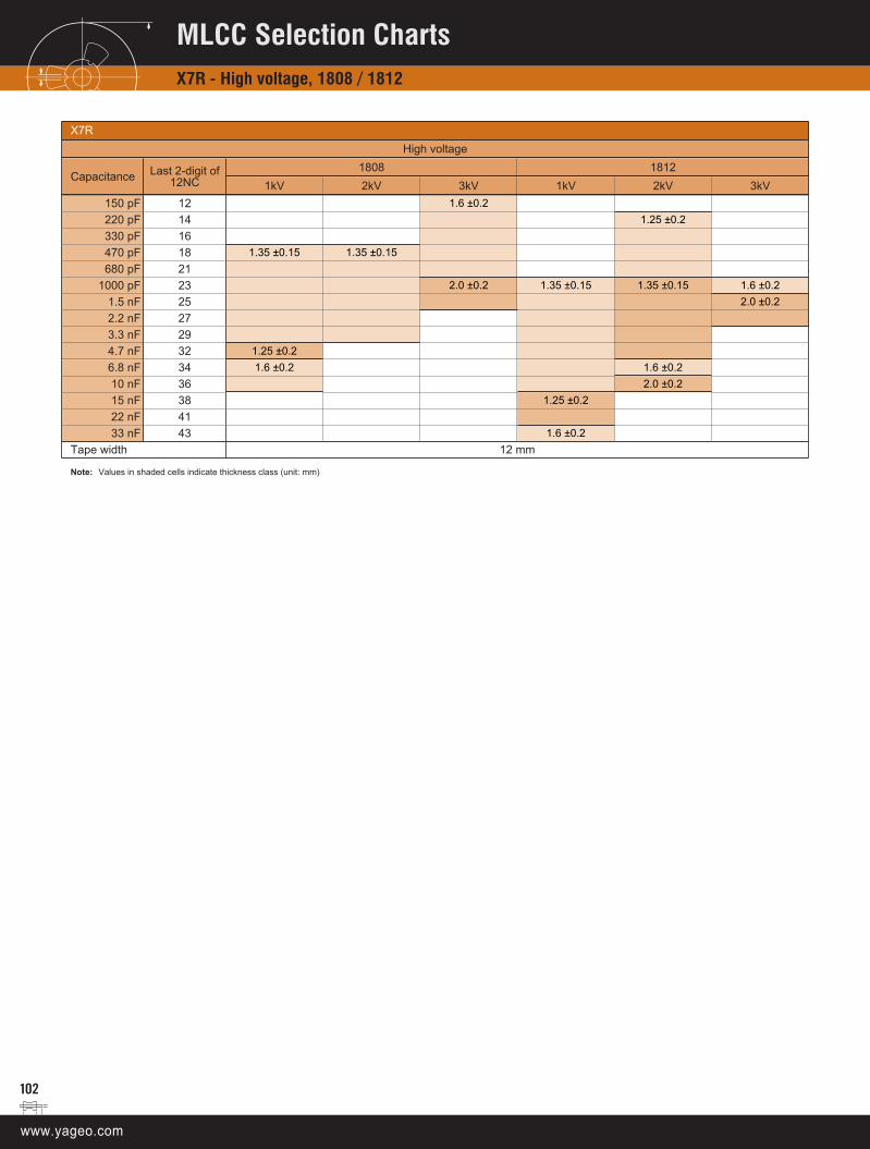
102
X7RHigh voltage
Capacitance Last 2-digit of12NC
1808 18121kV 2kV 3kV 1kV 2kV 3kV
150 pF 12 1.6 ±0.2220 pF 14 1.25 ±0.2330 pF 16470 pF 18 1.35 ±0.15 1.35 ±0.15680 pF 21
1000 pF 23 2.0 ±0.2 1.35 ±0.15 1.35 ±0.15 1.6 ±0.21.5 nF 25 2.0 ±0.22.2 nF 273.3 nF 294.7 nF 32 1.25 ±0.26.8 nF 34 1.6 ±0.2 1.6 ±0.210 nF 36 2.0 ±0.215 nF 38 1.25 ±0.222 nF 4133 nF 43 1.6 ±0.2
Tape width 12 mm
Note: Values in shaded cells indicate thickness class (unit: mm)
MLCC Selection ChartsX7R - High voltage, 1808 / 1812

103
Global part number - Preferred type
Global Part Number is the preferred clear text code for ordering Yageo and Phycomp branded products. For details, please see page 76.
12NC ordering code - Phycomp branded product only
2 2 X X X X X X X X X X
Carrier tape Capacitance value 38 = Paper (≥10 V ) See selection chart22 = Blister (≥10 V )50 = Blister (6.3 V / ≥1 kV) Tolerance55 = Paper (6.3 V / ≥1 kV) 5 = ±5%54 = Bulk 6 = ±10%
7 = ±20%Voltage
20 = 6.3 V TC material24 = 10 V 5 = X7R78 = 16 V91 = 25 V Packing58 = 50 V 1 = 180 mm / 7” reel60 = 100 V 5 = 330 mm / 13” reel93 = 200 V 4 = Bulk case83 = 250 V97 = 500 V98 = 630 V00 = 1 kV02 = 2 kV99 = 2.5 kV04 = 3 kV50 = 4 kV
Size8 = 02017 = 0402
6 = 06030 = 08051 = 12062 = 12103 = 18084 = 1812
Phycomp CTC ordering code - North America
Regional code for ordering Phycomp branded products. For details, please see page 77.
MLCC Selection ChartsX7R - General purpose, High Capacitance, Midium & High voltage

104
X7RLow inductance
Capacitance Last 2-digit of12NC
10V 16V 25V 50V0306 0508 0508 0612
10 nF 36 0.85 ±0.1 0.85 ±0.122 nF 4147 nF 45
100 nF 49 0.5 ±0.1 0.85 ±0.1220 nF 54
Tape width 8 mm
Note: Values in shaded cells indicate thickness class (unit: mm)
MLCC Selection ChartsX7R - Low inductance, 0306 to 0612
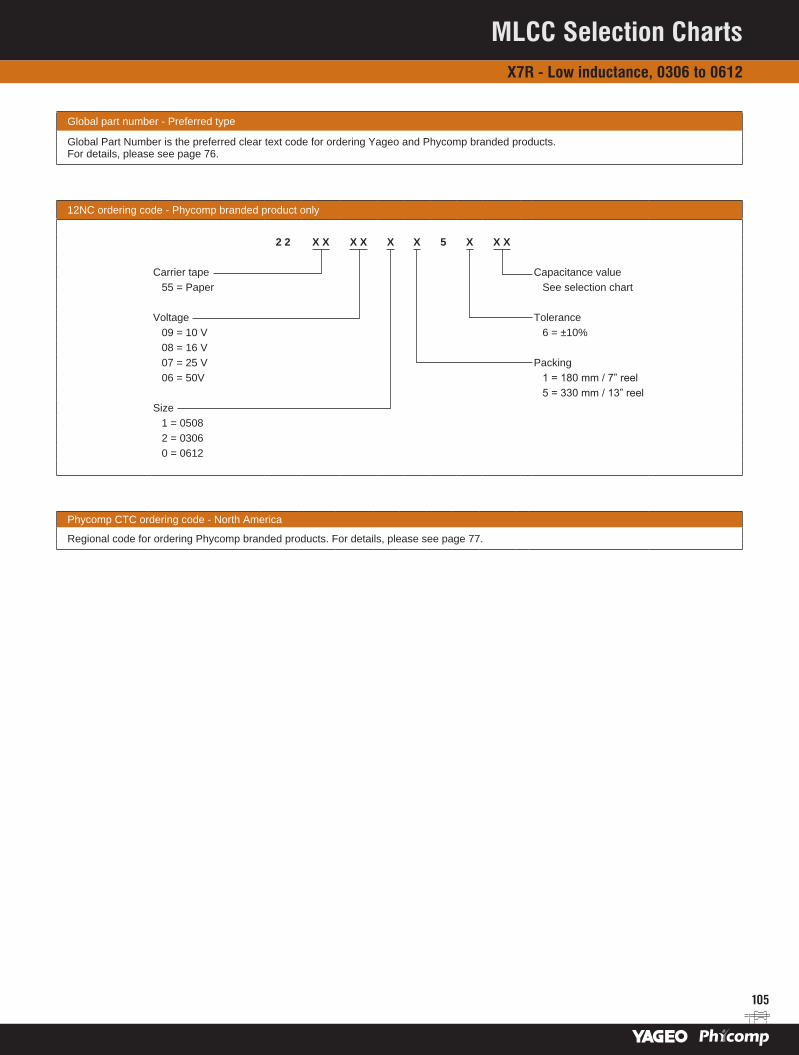
105
Global part number - Preferred type
Global Part Number is the preferred clear text code for ordering Yageo and Phycomp branded products. For details, please see page 76.
12NC ordering code - Phycomp branded product only
2 2 X X X X X X 5 X X X
Carrier tape Capacitance value 55 = Paper See selection chart
Voltage Tolerance09 = 10 V 6 = ±10%08 = 16 V07 = 25 V Packing06 = 50V 1 = 180 mm / 7” reel
5 = 330 mm / 13” reelSize
1 = 05082 = 03060 = 0612
Phycomp CTC ordering code - North America
Regional code for ordering Phycomp branded products. For details, please see page 77.
MLCC Selection ChartsX7R - Low inductance, 0306 to 0612

106
X5RGeneral purpose & High capacitance
Capacitance Last 2-digit of12NC
0201 04026.3V 10V 16V 6.3V 10V 16V
10 nF 36 0.3 ±0.03 0.3 ±0.03 0.3 ±0.03100 nF 49 0.5 ±0.05 0.5 ±0.05 0.5 ±0.05150 nF 52220 nF 54470 nF 58
1000 nF 63Tape width 8 mm
Note: Values in shaded cells indicate thickness class (unit: mm)
MLCC Selection ChartsX5R - General purpose & High capacitance, 0201 / 0402

107
X5RGeneral purpose & High capacitance
Capacitance Last 2-digit of12NC
0603 08056.3V 10V 16V 25V 6.3V 10V 16V 25V
330 nF 56 0.8 ±0.1 0.8 ±0.1470 nF 58 0.8 ±0.1 0.8 ±0.1
1000 nF 63 1.25 ±0.2 1.25 ±0.2 1.25 ±0.2 1.25 ±0.22.2 uF 67 0.85 ±0.1 0.85 ±0.1 0.85 ±0.14.7 uF 72 1.25 ±0.2 1.25 ±0.2 1.25 ±0.210 uF 7622 uF 81
Tape width 8 mm
Note: Values in shaded cells indicate thickness class (unit: mm)
MLCC Selection ChartsX5R - General purpose & High capacitance, 0603 / 0805

108
X5RHigh capacitance
Capacitance Last 2-digit of12NC
1206 1210 18126.3V 10V 16V 25V 6.3V 10V 16V 25V 6.3V 10V
2.2 uF 67 1.15 ±0.1 1.15 ±0.1 1.15 ±0.14.7 uF 72 1.15 ±0.1 1.6 ±0.2 1.9 ±0.2 1.9 ±0.210 uF 76 1.6 ±0.2 1.6 ±0.2 1.6 ±0.2 1.9 ±0.222 uF 81 2.0 ±0.2 2.0 ±0.2 2.5 ±0.2 2.5 ±0.2 2.5 ±0.247 uF 85 2.5 ±0.2
100 uF 89 3.2 ±0.3Tape width 8 mm 12 mm
Note: Values in shaded cells indicate thickness class (unit: mm)
MLCC Selection ChartsX5R - High capacitance, 1206 to 1812

109
Global part number - Preferred type
Global Part Number is the preferred clear text code for ordering Yageo and Phycomp branded products. For details, please see page 76.
12NC ordering code - Phycomp branded product only
2 2 X X X X X X X X X X
Carrier tape Capacitance value 50 = Blister (6.3 V) See selection chart55 = Paper (6.3 V)38 = Paper (≥10 V) Tolerance22 = Blister (≥10 V) 5 = ±5%54 = Bulk 6 = ±10%
7 = ±20%Voltage
20 = 6.3 V TC material24 = 10 V 3 = X5R78 = 16 V91 = 25 V Packing58 = 50 V 1 = 180 mm / 7” reel
5 = 330 mm / 13” reelSize 4 = Bulk case
8 = 02017 = 04026 = 06030 = 08051 = 12062 = 1210
4 = 1812
Phycomp CTC ordering code - North America
Regional code for ordering Phycomp branded products. For details, please see page 77.
MLCC Selection ChartsX5R - General purpose & High Capacitance, 0201 to 1812
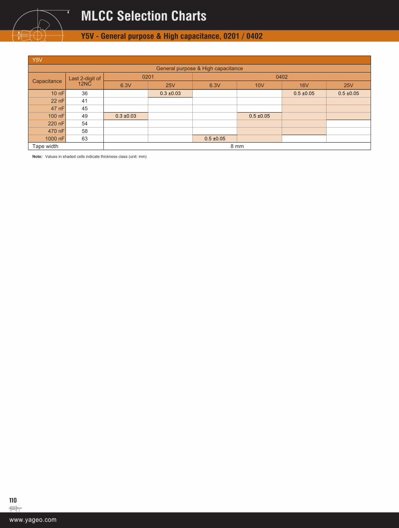
110
Y5VGeneral purpose & High capacitance
Capacitance Last 2-digit of12NC
0201 04026.3V 25V 6.3V 10V 16V 25V
10 nF 36 0.3 ±0.03 0.5 ±0.05 0.5 ±0.0522 nF 4147 nF 45
100 nF 49 0.3 ±0.03 0.5 ±0.05220 nF 54470 nF 58
1000 nF 63 0.5 ±0.05Tape width 8 mm
Note: Values in shaded cells indicate thickness class (unit: mm)
MLCC Selection ChartsY5V - General purpose & High capacitance, 0201 / 0402

111
Y5VGeneral purpose & High capacitance
Capacitance Last 2-digit of12NC
0603 08056.3V 10V 16V 25V 50V 6.3V 10V 16V 25V 50V
10 nF 36 0.8 ±0.1 0.8 ±0.1 0.6 ±0.1 0.6 ±0.1 0.6 ±0.122 nF 4147 nF 45
100 nF 49 0.8 ±0.1220 nF 54 0.85 ±0.1 0.85 ±0.1 0.85 ±0.1 0.85 ±0.1470 nF 58 0.8 ±0.1
1000 nF 63 1.25 ±0.22.2 uF 67 0.8 ±0.1 1.25 ±0.24.7 uF 72 1.25 ±0.210 uF 76 1.25 ±0.2 1.25 ±0.222 uF 81
Tape width 8 mm
Note: Values in shaded cells indicate thickness class (unit: mm)
MLCC Selection ChartsY5V - General purpose & High capacitance, 0603 / 0805
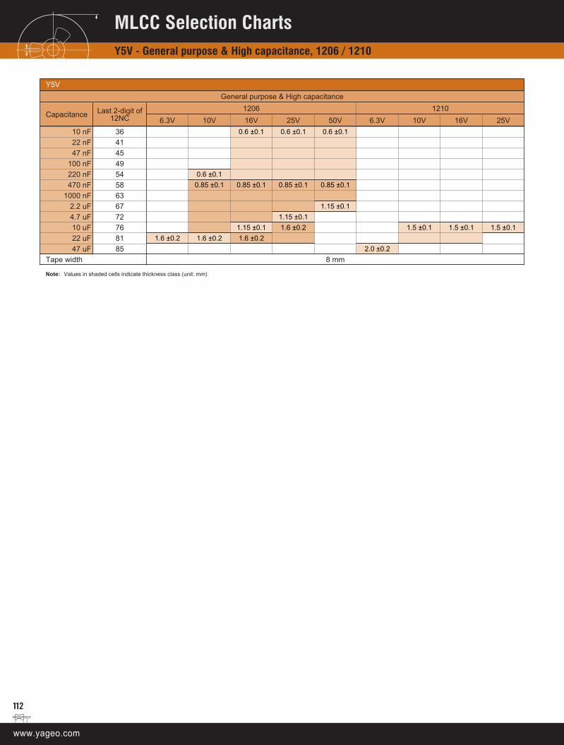
112
Y5VGeneral purpose & High capacitance
Capacitance Last 2-digit of12NC
1206 12106.3V 10V 16V 25V 50V 6.3V 10V 16V 25V
10 nF 36 0.6 ±0.1 0.6 ±0.1 0.6 ±0.122 nF 4147 nF 45
100 nF 49220 nF 54 0.6 ±0.1470 nF 58 0.85 ±0.1 0.85 ±0.1 0.85 ±0.1 0.85 ±0.1
1000 nF 632.2 uF 67 1.15 ±0.14.7 uF 72 1.15 ±0.110 uF 76 1.15 ±0.1 1.6 ±0.2 1.5 ±0.1 1.5 ±0.1 1.5 ±0.122 uF 81 1.6 ±0.2 1.6 ±0.2 1.6 ±0.247 uF 85 2.0 ±0.2
Tape width 8 mm
Note: Values in shaded cells indicate thickness class (unit: mm)
MLCC Selection ChartsY5V - General purpose & High capacitance, 1206 / 1210
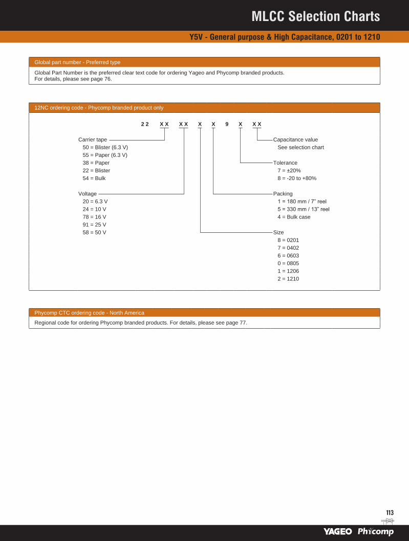
113
Global part number - Preferred type
Global Part Number is the preferred clear text code for ordering Yageo and Phycomp branded products. For details, please see page 76.
12NC ordering code - Phycomp branded product only
2 2 X X X X X X 9 X X X
Carrier tape Capacitance value 50 = Blister (6.3 V) See selection chart55 = Paper (6.3 V)38 = Paper Tolerance22 = Blister 7 = ±20%54 = Bulk 8 = -20 to +80%
Voltage Packing20 = 6.3 V 1 = 180 mm / 7” reel24 = 10 V 5 = 330 mm / 13” reel78 = 16 V 4 = Bulk case91 = 25 V58 = 50 V Size
8 = 02017 = 04026 = 06030 = 08051 = 12062 = 1210
Phycomp CTC ordering code - North America
Regional code for ordering Phycomp branded products. For details, please see page 77.
MLCC Selection ChartsY5V - General purpose & High Capacitance, 0201 to 1210
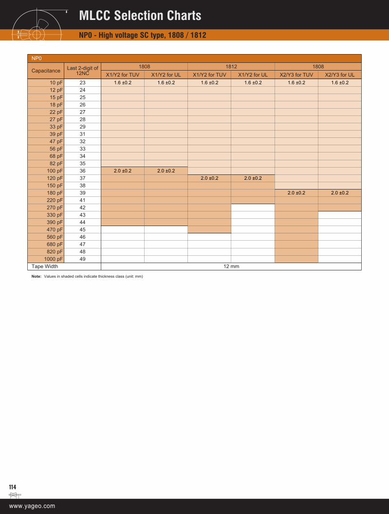
114
NP0
Capacitance Last 2-digit of12NC
1808 1812 1808X1/Y2 for TUV X1/Y2 for UL X1/Y2 for TUV X1/Y2 for UL X2/Y3 for TUV X2/Y3 for UL
10 pF 23 1.6 ±0.2 1.6 ±0.2 1.6 ±0.2 1.6 ±0.2 1.6 ±0.2 1.6 ±0.212 pF 2415 pF 2518 pF 2622 pF 2727 pF 2833 pF 2939 pF 3147 pF 3256 pF 3368 pF 3482 pF 35
100 pF 36 2.0 ±0.2 2.0 ±0.2120 pF 37 2.0 ±0.2 2.0 ±0.2150 pF 38180 pF 39 2.0 ±0.2 2.0 ±0.2220 pF 41270 pF 42330 pF 43390 pF 44470 pF 45560 pF 46680 pF 47820 pF 48
1000 pF 49Tape Width 12 mm
Note: Values in shaded cells indicate thickness class (unit: mm)
MLCC Selection ChartsNP0 - High voltage SC type, 1808 / 1812
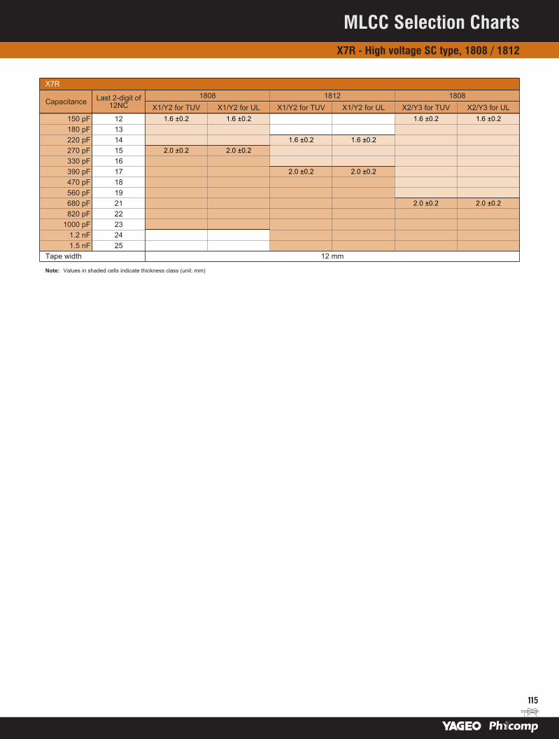
115
X7R
Capacitance Last 2-digit of12NC
1808 1812 1808X1/Y2 for TUV X1/Y2 for UL X1/Y2 for TUV X1/Y2 for UL X2/Y3 for TUV X2/Y3 for UL
150 pF 12 1.6 ±0.2 1.6 ±0.2 1.6 ±0.2 1.6 ±0.2180 pF 13220 pF 14 1.6 ±0.2 1.6 ±0.2270 pF 15 2.0 ±0.2 2.0 ±0.2330 pF 16390 pF 17 2.0 ±0.2 2.0 ±0.2470 pF 18560 pF 19680 pF 21 2.0 ±0.2 2.0 ±0.2820 pF 22
1000 pF 231.2 nF 241.5 nF 25
Tape width 12 mm
Note: Values in shaded cells indicate thickness class (unit: mm)
MLCC Selection ChartsX7R - High voltage SC type, 1808 / 1812
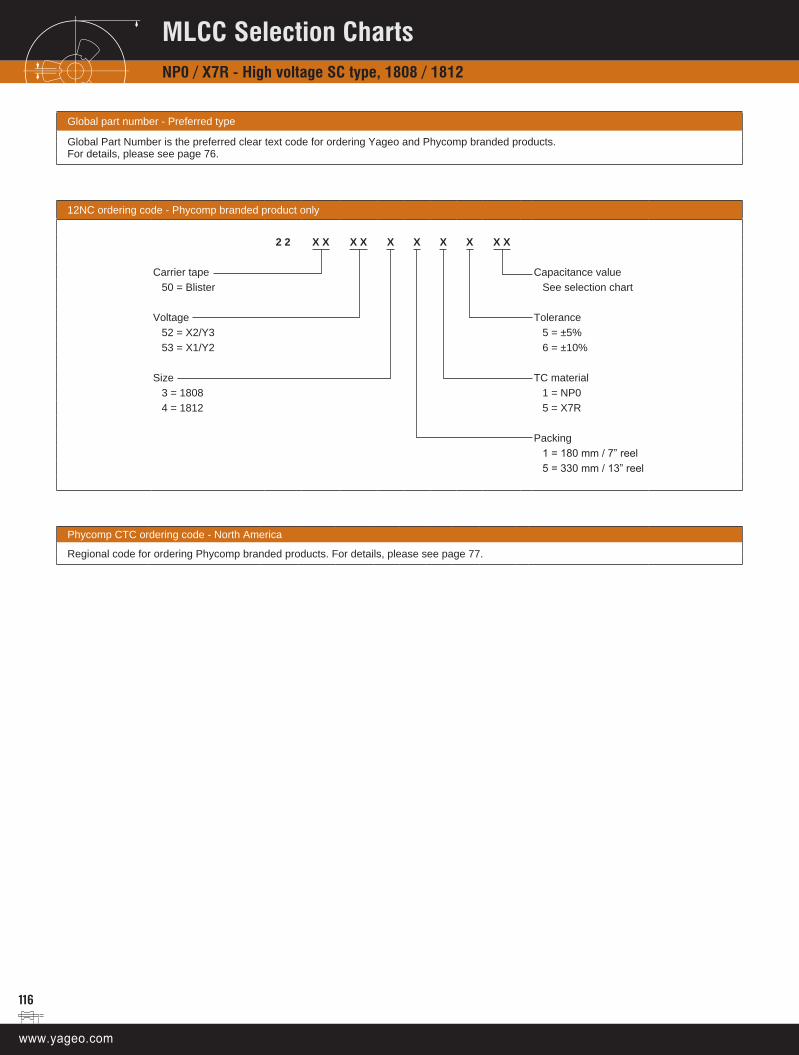
116
Global part number - Preferred type
Global Part Number is the preferred clear text code for ordering Yageo and Phycomp branded products. For details, please see page 76.
12NC ordering code - Phycomp branded product only
2 2 X X X X X X X X X X
Carrier tape Capacitance value 50 = Blister See selection chart
Voltage Tolerance52 = X2/Y3 5 = ±5%53 = X1/Y2 6 = ±10%
Size TC material3 = 1808 1 = NP04 = 1812 5 = X7R
Packing1 = 180 mm / 7” reel5 = 330 mm / 13” reel
Phycomp CTC ordering code - North America
Regional code for ordering Phycomp branded products. For details, please see page 77.
MLCC Selection ChartsNP0 / X7R - High voltage SC type, 1808 / 1812
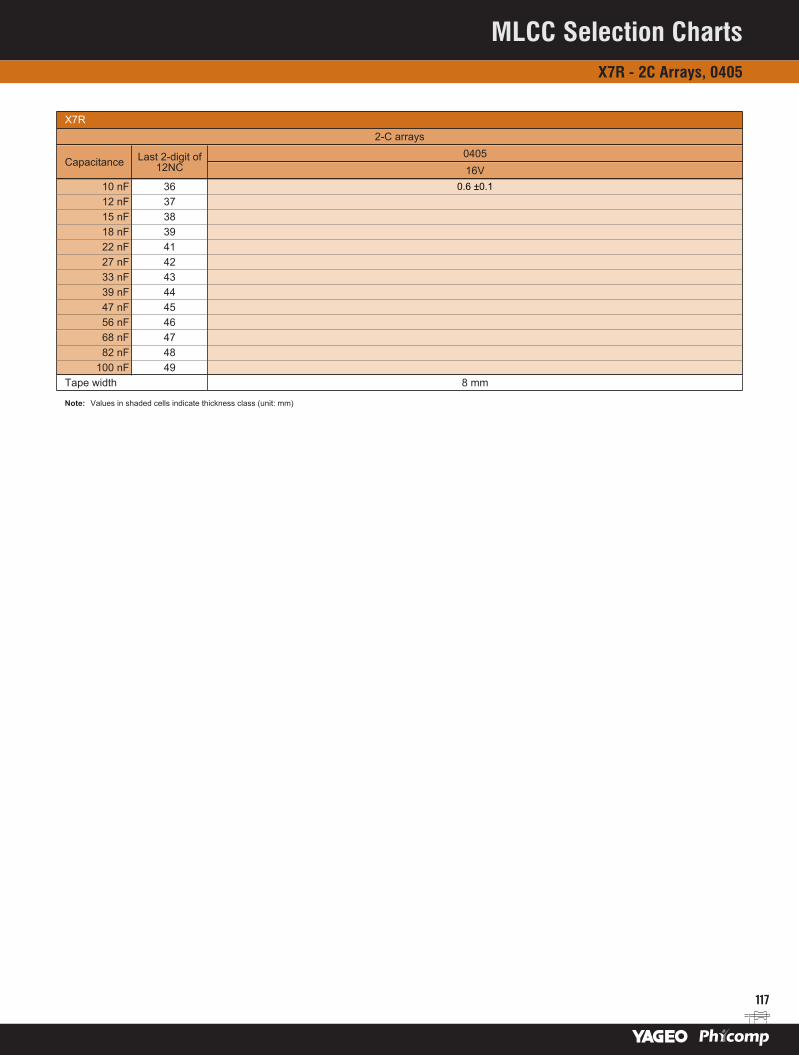
117
X7R2-C arrays
Capacitance Last 2-digit of12NC
040516V
10 nF 36 0.6 ±0.112 nF 3715 nF 3818 nF 3922 nF 4127 nF 4233 nF 4339 nF 4447 nF 4556 nF 4668 nF 4782 nF 48
100 nF 49Tape width 8 mm
Note: Values in shaded cells indicate thickness class (unit: mm)
MLCC Selection ChartsX7R - 2C Arrays, 0405

118
Global part number - Preferred type
Global Part Number is the preferred clear text code for ordering Yageo and Phycomp branded products. For details, please see page 76.
12NC ordering code - Phycomp branded product only
2 2 X X X X 2 X X X X X
Carrier tape Capacitance value 50 = Blister See selection chart55 = Paper
ToleranceVoltage 6 = ±10%
70 = 16 V 7 = ±20%
Packing TC material1 = 180 mm / 7” reel 5 = X7R
Phycomp CTC ordering code - North America
Regional code for ordering Phycomp branded products. For details, please see page 77.
MLCC Selection ChartsX7R - 2C Arrays, 0405

119
NP04-C arrays
Capacitance Last 2-digit of12NC
0508 061250V 50V
10 pF 23 0.6 ±0.1 0.8 ±0.115 pF 2518 pF 2622 pF 2727 pF 2847 pF 32
100 pF 36150 pF 38180 pF 39220 pF 41270 pF 42330 pF 43390 pF 44470 pF 45560 pF 46680 pF 47820 pF 48
1000 pF 49Tape width 8 mm
Note: Values in shaded cells indicate thickness class (unit: mm)
MLCC Selection ChartsNP0 - 4C Arrays, 0508 / 0612
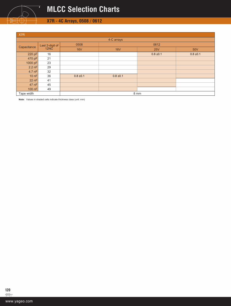
120
X7R4-C arrays
Capacitance Last 2-digit of12NC
0508 061216V 16V 25V 50V
220 pF 16 0.8 ±0.1 0.8 ±0.1470 pF 21
1000 pF 232.2 nF 294.7 nF 3210 nF 36 0.8 ±0.1 0.8 ±0.122 nF 4147 nF 45
100 nF 49Tape width 8 mm
Note: Values in shaded cells indicate thickness class (unit: mm)
MLCC Selection ChartsX7R - 4C Arrays, 0508 / 0612

121
Y5V4-C arrays
Capacitance Last 2-digit of12NC
0508 061225V 25V
10 nF 36 0.6 ±0.1 0.6 ±0.122 nF 4147 nF 45
100 nF 49Tape width 8 mm
Note: Values in shaded cells indicate thickness class (unit: mm)
MLCC Selection ChartsY5V - 4C Arrays, 0508 / 0612

122
Global part number - Preferred type
Global Part Number is the preferred clear text code for ordering Yageo and Phycomp branded products. For details, please see page 76.
12NC ordering code - Phycomp branded product only
2 2 X X X X X X X X X X
Carrier tape Capacitance value 50 = Blister See selection chart55 = Paper
ToleranceVoltage 5 = ±5%
10 = 16 V 6 = ±10%12 = 25 V 7 = ±20%14 = 50 V 8 = -20 to +80%
Size TC material6 = 0612 (4 x 0603) 1 = NP07 = 0508 (4 x 0402) 5 = X7R
9 = Y5VPacking
1 = 180 mm / 7” reel
Phycomp CTC ordering code - North America
Regional code for ordering Phycomp branded products. For details, please see page 77.
MLCC Selection ChartsNP0 / X7R / Y5V - 4C Arrays, 0508 / 0612

123
0201 sample kitsNP0 50 V NP0 25 V X7R 50 V
Capacitance (pF) Tolerance Capacitance (pF) Tolerance Capacitance (pF) Tolerance1 ±0.25 pF 27 ±5% 47 ±10%1.2 ±0.25 pF 33 ±5% 68 ±10%1.5 ±0.25 pF 39 ±5% 100 ±10%1.8 ±0.25 pF 47 ±5% 150 ±10%2.2 ±0.25 pF 56 ±5% 220 ±10%2.7 ±0.25 pF 68 ±5% 330 ±10%3.3 ±0.25 pF 82 ±5% 470 ±10%3.9 ±0.25 pF 100 ±5% X7R 25 V4.7 ±0.25 pF Y5V 6.3V Capacitance (pF) Tolerance 5.6 ±0.50 pF Capacitance (pF) Tolerance 680 ±10%6.8 ±0.50 pF 100 000 -20% to +80% 1 000 ±10%8.2 ±0.50 pF X5R 6.3V X7R 16V
10 ±5% Capacitance (pF) Tolerance Capacitance (pF) Tolerance 12 ±5% 100 000 ±10% 1 500 ±10%15 ±5% 2 200 ±10%18 ±5% 3 300 ±10%22 ±5% X7R 10 V
Capacitance (pF) Tolerance 10 000 ±10%
Note: 100 pieces per value. Ordering code 432204407111 for Phycomp brand product, CC020100000000000 for Yageo brand product
0402 sample kitsNP0 50 V Y5V 16 V X7R 50 V
Capacitance (pF) Tolerance Capacitance (pF) Tolerance Capacitance (pF) Tolerance0.47 ±0.25 pF 10 000 ±20% 100 ±10%0.68 ±0.25 pF 22 000 ±20% 150 ±10%1 ±0.25 pF 47 000 ±20% 220 ±10%1.5 ±0.25 pF 100 000 ±20% 330 ±10%2.2 ±0.25 pF 470 ±10%3.3 ±0.25 pF 680 ±10%4.7 ±0.25 pF 1 000 ±10%6.8 ±0.50 pF 1 500 ±10%
10 ±5% 2 200 ±10%15 ±5% 3 300 ±10%22 ±5% X7R 25 V33 ±5% Capacitance (pF) Tolerance47 ±5% 4 700 ±10%68 ±5% X7R 16 V
100 ±5% Capacitance (pF) Tolerance150 ±5% 6 800 ±10%220 ±5% 10 000 ±10%
15 000 ±10%22 000 ±10%
Note: 95 pieces per value. Ordering code 432204409911 for Phycomp brand product, CC040200000000000 for Yageo brand product
MLCC Engineering Design KitsSample kits for 0201 / 0402
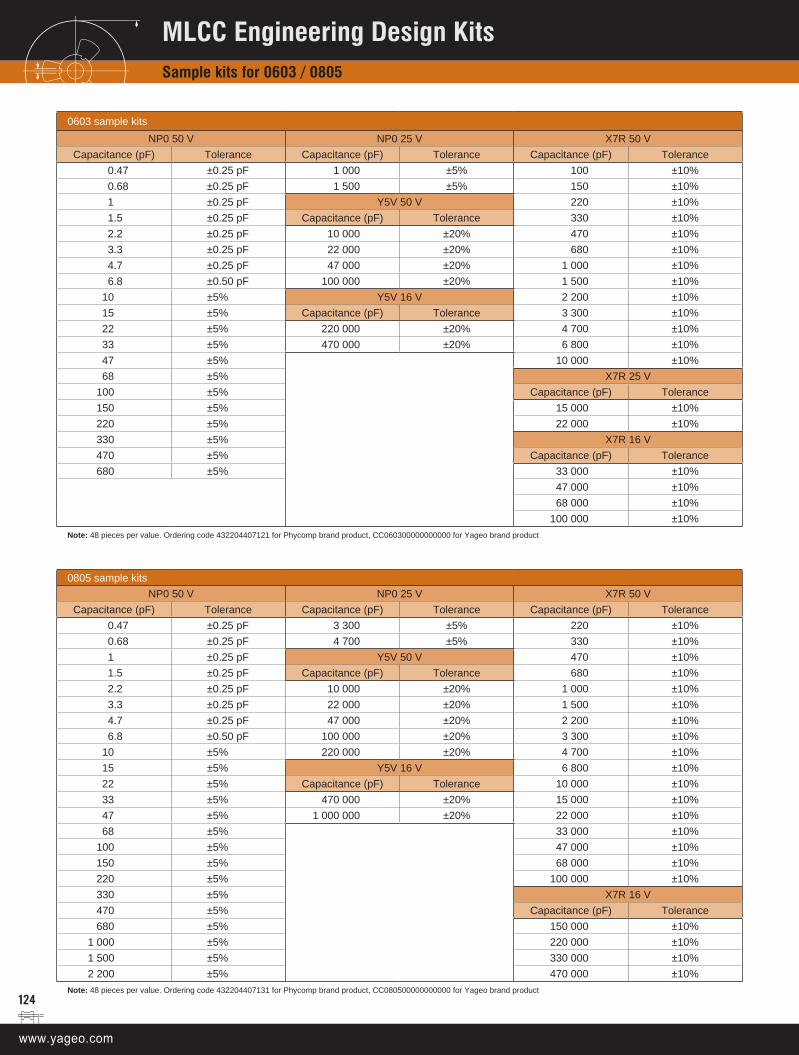
124
0603 sample kitsNP0 50 V NP0 25 V X7R 50 V
Capacitance (pF) Tolerance Capacitance (pF) Tolerance Capacitance (pF) Tolerance0.47 ±0.25 pF 1 000 ±5% 100 ±10%0.68 ±0.25 pF 1 500 ±5% 150 ±10%1 ±0.25 pF Y5V 50 V 220 ±10%1.5 ±0.25 pF Capacitance (pF) Tolerance 330 ±10%2.2 ±0.25 pF 10 000 ±20% 470 ±10%3.3 ±0.25 pF 22 000 ±20% 680 ±10%4.7 ±0.25 pF 47 000 ±20% 1 000 ±10%6.8 ±0.50 pF 100 000 ±20% 1 500 ±10%
10 ±5% Y5V 16 V 2 200 ±10%15 ±5% Capacitance (pF) Tolerance 3 300 ±10%22 ±5% 220 000 ±20% 4 700 ±10%33 ±5% 470 000 ±20% 6 800 ±10%47 ±5% 10 000 ±10%68 ±5% X7R 25 V
100 ±5% Capacitance (pF) Tolerance150 ±5% 15 000 ±10%220 ±5% 22 000 ±10%330 ±5% X7R 16 V470 ±5% Capacitance (pF) Tolerance680 ±5% 33 000 ±10%
47 000 ±10%68 000 ±10%
100 000 ±10%Note: 48 pieces per value. Ordering code 432204407121 for Phycomp brand product, CC060300000000000 for Yageo brand product
0805 sample kitsNP0 50 V NP0 25 V X7R 50 V
Capacitance (pF) Tolerance Capacitance (pF) Tolerance Capacitance (pF) Tolerance0.47 ±0.25 pF 3 300 ±5% 220 ±10%0.68 ±0.25 pF 4 700 ±5% 330 ±10%1 ±0.25 pF Y5V 50 V 470 ±10%1.5 ±0.25 pF Capacitance (pF) Tolerance 680 ±10%2.2 ±0.25 pF 10 000 ±20% 1 000 ±10%3.3 ±0.25 pF 22 000 ±20% 1 500 ±10%4.7 ±0.25 pF 47 000 ±20% 2 200 ±10%6.8 ±0.50 pF 100 000 ±20% 3 300 ±10%
10 ±5% 220 000 ±20% 4 700 ±10%15 ±5% Y5V 16 V 6 800 ±10%22 ±5% Capacitance (pF) Tolerance 10 000 ±10%33 ±5% 470 000 ±20% 15 000 ±10%47 ±5% 1 000 000 ±20% 22 000 ±10%68 ±5% 33 000 ±10%
100 ±5% 47 000 ±10%150 ±5% 68 000 ±10%220 ±5% 100 000 ±10%330 ±5% X7R 16 V470 ±5% Capacitance (pF) Tolerance680 ±5% 150 000 ±10%
1 000 ±5% 220 000 ±10%1 500 ±5% 330 000 ±10%2 200 ±5% 470 000 ±10%
Note: 48 pieces per value. Ordering code 432204407131 for Phycomp brand product, CC080500000000000 for Yageo brand product
MLCC Engineering Design KitsSample kits for 0603 / 0805

125
1206 sample kitsNP0 50 V NP0 25 V X7R 50 V
Capacitance (pF) Tolerance Capacitance (pF) Tolerance Capacitance (pF) Tolerance0.47 ±0.25 pF 10 000 ±5% 220 ±10%0.68 ±0.25 pF Y5V 50 V 330 ±10%1 ±0.25 pF Capacitance (pF) Tolerance 470 ±10%1.5 ±0.25 pF 100 000 ±20% 680 ±10%2.2 ±0.25 pF 220 000 ±20% 1 000 ±10%3.3 ±0.25 pF 470 000 ±20% 1 500 ±10%4.7 ±0.25 pF 1 000 000 ±20% 2 200 ±10%6.8 ±0.50 pF 3 300 ±10%
10 ±5% 4 700 ±10%15 ±5% 6 800 ±10%22 ±5% 10 000 ±10%33 ±5% 15 000 ±10%47 ±5% 22 000 ±10%68 ±5% 33 000 ±10%
100 ±5% 47 000 ±10%150 ±5% 68 000 ±10%220 ±5% 100 000 ±10%330 ±5% 150 000 ±10%470 ±5% 220 000 ±10%680 ±5% X7R 16 V
1 000 ±5% Capacitance (pF) Tolerance1 500 ±5% 330 000 ±10%2 200 ±5% 470 000 ±10%3 300 ±5% 680 000 ±10%4 700 ±5% 1 000 000 ±10%6 800 ±5%
Note: 48 pieces per value. Ordering code 432204407141 for Phycomp brand product, CC120600000000000 for Yageo brand product
MLCC Engineering Design KitsSample kits for 1206

126
High capacitance sample kitsX5R 0402 X7R 0603 Y5V 0402
Capacitance Rated voltage Tolerance Capacitance Rated voltage Tolerance Capacitance Rated voltage Tolerance 1 µF 6.3 V ±10% 1 µF 16 V ±10% 1 µF 6.3 V -20% to +80%1 µF 10 V ±10% X7R 0805 1 µF 10 V -20% to +80%
2.2 µF 6.3 V ±20% Capacitance Rated voltage Tolerance Y5V 0603X5R 0603 1 µF 25 V ±10% Capacitance Rated voltage Tolerance
Capacitance Rated voltage Tolerance 2.2 µF 16 V ±10% 1 µF 10 V -20% to +80%1 µF 16 V ±10% 2.2 µF 25 V ±10% 1 µF 16 V -20% to +80%1 µF 25 V ±10% X7R 1206 2.2 µF 10 V -20% to +80%
2.2 µF 6.3 V ±10% Capacitance Rated voltage Tolerance 2.2 µF 16 V -20% to +80%2.2 µF 10 V ±10% 1 µF 25 V ±10% 4.7 µF 6.3 V -20% to +80%2.2 µF 16 V ±10% 2.2 µF 25 V ±10% Y5V 08054.7 µF 6.3 V ±10% 4.7 µF 25 V ±10% Capacitance Rated voltage Tolerance 4.7 µF 10 V ±10% 10 µF 16 V ±10% 1 µF 16 V -20% to +80%10 µF 6.3 V ±20% 10 µF 25 V ±10% 1 µF 25 V -20% to +80%
X5R 0805 1 µF 50 V -20% to +80%Capacitance Rated voltage Tolerance 2.2 µF 16 V -20% to +80%
2.2 µF 25 V ±10% 4.7 µF 10 V -20% to +80%4.7 µF 6.3 V ±10% 10 µF 10 V -20% to +80%4.7 µF 10 V ±10% Y5V 12064.7 µF 16 V ±10% Capacitance Rated voltage Tolerance 10 µF 6.3 V ±10% 4.7 µF 16 V -20% to +80%10 µF 10 V ±10% 10 µF 10 V -20% to +80%10 µF 16 V ±10% 10 µF 16 V -20% to +80%22 µF 6.3 V ±20% 22 µF 16 V -20% to +80%
X5R 1206Capacitance Rated voltage Tolerance
4.7 µF 16 V ±10%4.7 µF 25 V ±10%10 µF 16 V ±10%10 µF 25 V ±10%22 µF 6.3 V ±20%
Note: 50 pieces per value. Ordering code 432204510001 for Phycomp brand product, CC888800000000000 for Yageo brand product
MLCC Engineering Design KitsSample kits for high capacitance series
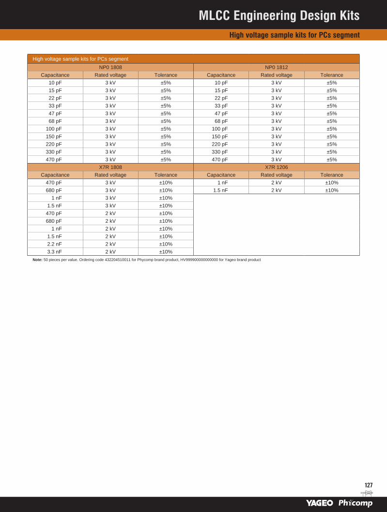
127
High voltage sample kits for PCs segmentNP0 1808 NP0 1812
Capacitance Rated voltage Tolerance Capacitance Rated voltage Tolerance10 pF 3 kV ±5% 10 pF 3 kV ±5%15 pF 3 kV ±5% 15 pF 3 kV ±5%22 pF 3 kV ±5% 22 pF 3 kV ±5%33 pF 3 kV ±5% 33 pF 3 kV ±5%47 pF 3 kV ±5% 47 pF 3 kV ±5%68 pF 3 kV ±5% 68 pF 3 kV ±5%
100 pF 3 kV ±5% 100 pF 3 kV ±5%150 pF 3 kV ±5% 150 pF 3 kV ±5%220 pF 3 kV ±5% 220 pF 3 kV ±5%330 pF 3 kV ±5% 330 pF 3 kV ±5%470 pF 3 kV ±5% 470 pF 3 kV ±5%
X7R 1808 X7R 1206Capacitance Rated voltage Tolerance Capacitance Rated voltage Tolerance
470 pF 3 kV ±10% 1 nF 2 kV ±10%680 pF 3 kV ±10% 1.5 nF 2 kV ±10%
1 nF 3 kV ±10%1.5 nF 3 kV ±10%
470 pF 2 kV ±10%680 pF 2 kV ±10%
1 nF 2 kV ±10%1.5 nF 2 kV ±10%2.2 nF 2 kV ±10%3.3 nF 2 kV ±10%
Note: 50 pieces per value. Ordering code 432204510011 for Phycomp brand product, HV999900000000000 for Yageo brand product
MLCC Engineering Design KitsHigh voltage sample kits for PCs segment

128
High voltage sample kits for inverter segmentNP0 1808
Capacitance Rated voltage Tolerance5 pF 3 kV ±5%
10 pF 3 kV ±5%12 pF 3 kV ±5%15 pF 3 kV ±5%18 pF 3 kV ±5%22 pF 3 kV ±5%27 pF 3 kV ±5%33 pF 3 kV ±5%39 pF 3 kV ±5%47 pF 3 kV ±5%56 pF 3 kV ±5%68 pF 3 kV ±5%82 pF 3 kV ±5%
100 pF 3 kV ±5%120 pF 3 kV ±5%150 pF 3 kV ±5%220 pF 3 kV ±5%330 pF 3 kV ±5%470 pF 3 kV ±5%
Note: 50 pieces per value. Ordering code 432204510012 for Phycomp brand product, HV888800000000000 for Yageo brand product
MLCC Engineering Design KitsHigh voltage sample kits for inverter segment

129
High voltage sample kits for general applicationNP0 1206 X7R 1206
Capacitance Rated voltage Tolerance Capacitance Rated voltage Tolerance10 pF 1 kV ±5% 10 nF 1 kV ±10%
100 pF 1 kV ±5% 1 nF 2 kV ±10%1 nF 1 kV ±5% 1 nF 1 kV ±10%
10 pF 2 kV ±5% X7R 1210100 pF 2 kV ±5% Capacitance Rated voltage Tolerance
NP0 1210 1 nF 1 kV ±10%Capacitance Rated voltage Tolerance 10 nF 1 kV ±10%
10 pF 1 kV ±5% 1 nF 2 kV ±10%100 pF 1 kV ±5% X7R 1808
1 nF 1 kV ±5% Capacitance Rated voltage Tolerance10 pF 2 kV ±5% 10 nF 1 kV ±10%
100 pF 2 kV ±5% 1 nF 3 kV ±10%NP0 1808 1 nF 1 kV ±10%
Capacitance Rated voltage Tolerance 1 nF 2 kV ±10%10 pF 1 kV ±5% X7R 1812
100 pF 1 kV ±5% Capacitance Rated voltage Tolerance1 nF 1 kV ±5% 10 nF 2 kV ±10%
10 pF 3 kV ±5% 1 nF 1 kV ±10%100 pF 3 kV ±5% 10 nF 1 kV ±10%
10 pF 4 kV ±5%10 pF 2 kV ±5%
100 pF 2 kV ±5%NP0 1812
Capacitance Rated voltage Tolerance10 pF 2 kV ±5%
100 pF 2 kV ±5%1 nF 2 kV ±5%
10 pF 1 kV ±5%100 pF 1 kV ±5%
1 nF 1 kV ±5%10 pF 3 kV ±5%
100 pF 3 kV ±5%10 nF 4 kV ±5%
Note: 50 pieces per value. Ordering code 432204510013 for Phycomp brand product, HV777700000000000 for Yageo brand product
MLCC Engineering Design KitsHigh voltage sample kits for general application
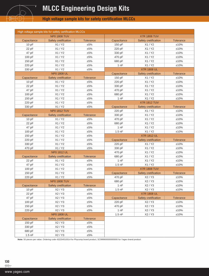
130
High voltage sample kits for safety certification MLCCsNP0 1808 TUV X7R 1808 TUV
Capacitance Safety cretification Tolerance Capacitance Safety cretification Tolerance10 pF X1 / Y2 ±5% 150 pF X1 / Y2 ±10%22 pF X1 / Y2 ±5% 220 pF X1 / Y2 ±10%47 pF X1 / Y2 ±5% 330 pF X1 / Y2 ±10%
100 pF X1 / Y2 ±5% 470 pF X1 / Y2 ±10%150 pF X1 / Y2 ±5% 680 pF X1 / Y2 ±10%220 pF X1 / Y2 ±5% 1 nF X1 / Y2 ±10%330 pF X1 / Y2 ±5% X7R 1808 UL
NP0 1808 UL Capacitance Safety cretification ToleranceCapacitance Safety cretification Tolerance 150 pF X1 / Y2 ±10%
10 pF X1 / Y2 ±5% 220 pF X1 / Y2 ±10%22 pF X1 / Y2 ±5% 330 pF X1 / Y2 ±10%47 pF X1 / Y2 ±5% 470 pF X1 / Y2 ±10%
100 pF X1 / Y2 ±5% 680 pF X1 / Y2 ±10%150 pF X1 / Y2 ±5% 1 nF X1 / Y2 ±10%220 pF X1 / Y2 ±5% X7R 1812 TUV330 pF X1 / Y2 ±5% Capacitance Safety cretification Tolerance
NP0 1812 TUV 220 pF X1 / Y2 ±10%Capacitance Safety cretification Tolerance 330 pF X1 / Y2 ±10%
10 pF X1 / Y2 ±5% 470 pF X1 / Y2 ±10%22 pF X1 / Y2 ±5% 680 pF X1 / Y2 ±10%47 pF X1 / Y2 ±5% 1 nF X1 / Y2 ±10%
100 pF X1 / Y2 ±5% 1.5 nF X1 / Y2 ±10%150 pF X1 / Y2 ±5% X7R 1812 UL220 pF X1 / Y2 ±5% Capacitance Safety cretification Tolerance330 pF X1 / Y2 ±5% 220 pF X1 / Y2 ±10%470 pF X1 / Y2 ±5% 330 pF X1 / Y2 ±10%
NP0 1812 UL 470 pF X1 / Y2 ±10%Capacitance Safety cretification Tolerance 680 pF X1 / Y2 ±10%
22 pF X1 / Y2 ±5% 1 nF X1 / Y2 ±10%47 pF X1 / Y2 ±5% 1.5 nF X1 / Y2 ±10%
100 pF X1 / Y2 ±5% X7R 1808 TUV150 pF X1 / Y2 ±5% Capacitance Safety cretification Tolerance220 pF X1 / Y2 ±5% 470 pF X2 / Y3 ±10%
NP0 1808 TUV 680 pF X2 / Y3 ±10%Capacitance Safety cretification Tolerance 1 nF X2 / Y3 ±10%
10 pF X2 / Y3 ±5% 1.5 nF X2 / Y3 ±10%22 pF X2 / Y3 ±5% X7R 1808 UL47 pF X2 / Y3 ±5% Capacitance Safety cretification Tolerance
100 pF X2 / Y3 ±5% 220 pF X2 / Y3 ±10%150 pF X2 / Y3 ±5% 470 pF X2 / Y3 ±10%220 pF X2 / Y3 ±5% 1 nF X2 / Y3 ±10%
NP0 1808 UL 1.5 nF X2 / Y3 ±10%Capacitance Safety cretification Tolerance
150 pF X2 / Y3 ±5%330 pF X2 / Y3 ±5%680 pF X2 / Y3 ±5%1.5 nF X2 / Y3 ±5%
Note: 50 pieces per value. Ordering code 432204510014 for Phycomp brand product, SC999900000000000 for Yageo brand product
MLCC Engineering Design KitsHigh voltage sample kits for safety certification MLCCs
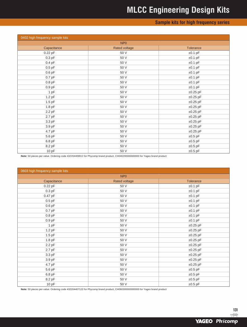
131
0402 high frequency sample kitsNP0
Capacitance Rated voltage Tolerance0.22 pF 50 V ±0.1 pF
0.3 pF 50 V ±0.1 pF0.4 pF 50 V ±0.1 pF0.5 pF 50 V ±0.1 pF0.6 pF 50 V ±0.1 pF0.7 pF 50 V ±0.1 pF0.8 pF 50 V ±0.1 pF0.9 pF 50 V ±0.1 pF
1 pF 50 V ±0.25 pF1.2 pF 50 V ±0.25 pF1.5 pF 50 V ±0.25 pF1.8 pF 50 V ±0.25 pF2.2 pF 50 V ±0.25 pF2.7 pF 50 V ±0.25 pF3.3 pF 50 V ±0.25 pF3.9 pF 50 V ±0.25 pF4.7 pF 50 V ±0.25 pF5.6 pF 50 V ±0.5 pF6.8 pF 50 V ±0.5 pF8.2 pF 50 V ±0.5 pF10 pF 50 V ±0.5 pF
Note: 50 pieces per value. Ordering code 432204409912 for Phycomp brand product, CH040200000000000 for Yageo brand product
0603 high frequency sample kitsNP0
Capacitance Rated voltage Tolerance0.22 pF 50 V ±0.1 pF
0.3 pF 50 V ±0.1 pF0.47 pF 50 V ±0.1 pF
0.5 pF 50 V ±0.1 pF0.6 pF 50 V ±0.1 pF0.7 pF 50 V ±0.1 pF0.8 pF 50 V ±0.1 pF0.9 pF 50 V ±0.1 pF
1 pF 50 V ±0.25 pF1.2 pF 50 V ±0.25 pF1.5 pF 50 V ±0.25 pF1.8 pF 50 V ±0.25 pF2.2 pF 50 V ±0.25 pF2.7 pF 50 V ±0.25 pF3.3 pF 50 V ±0.25 pF3.9 pF 50 V ±0.25 pF4.7 pF 50 V ±0.25 pF5.6 pF 50 V ±0.5 pF6.8 pF 50 V ±0.5 pF8.2 pF 50 V ±0.5 pF10 pF 50 V ±0.5 pF
Note: 50 pieces per value. Ordering code 432204407122 for Phycomp brand product, CH060300000000000 for Yageo brand product
MLCC Engineering Design KitsSample kits for high frequency series
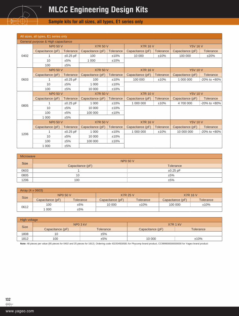
132
All sizes, all types, E1 series onlyGeneral purpose & High capacitance
0402
NP0 50 V X7R 50 V X7R 16 V Y5V 16 VCapacitance (pF) Tolerance Capacitance (pF) Tolerance Capacitance (pF) Tolerance Capacitance (pF) Tolerance
1 ±0.25 pF 100 ±10% 10 000 ±10% 100 000 ±20%10 ±5% 1 000 ±10%
100 ±5%
0603
NP0 50 V X7R 50 V X7R 16 V Y5V 10 VCapacitance (pF) Tolerance Capacitance (pF) Tolerance Capacitance (pF) Tolerance Capacitance (pF) Tolerance
1 ±0.25 pF 100 ±10% 100 000 ±10% 1 000 000 -20% to +80%10 ±5% 1 000 ±10%
100 ±5% 10 000 ±10%
0805
NP0 50 V X7R 50 V X7R 10 V Y5V 10 VCapacitance (pF) Tolerance Capacitance (pF) Tolerance Capacitance (pF) Tolerance Capacitance (pF) Tolerance
1 ±0.25 pF 1 000 ±10% 1 000 000 ±10% 4 700 000 -20% to +80%10 ±5% 10 000 ±10%
100 ±5% 100 000 ±10%1 000 ±5%
1206
NP0 50 V X7R 50 V X7R 16 V Y5V 10 VCapacitance (pF) Tolerance Capacitance (pF) Tolerance Capacitance (pF) Tolerance Capacitance (pF) Tolerance
1 ±0.25 pF 1 000 ±10% 1 000 000 ±10% 10 000 000 -20% to +80%10 ±5% 10 000 ±10%
100 ±5% 100 000 ±10%1 000 ±5%
Microwave
SizeNP0 50 V
Capacitance (pF) Tolerance0603 1 ±0.25 pF0805 10 ±5%1206 100 ±5%
Array (4 x 0603)
SizeNP0 50 V X7R 25 V X7R 16 V
Capacitance (pF) Tolerance Capacitance (pF) Tolerance Capacitance (pF) Tolerance
0612100 ±5% 10 000 ±10% 100 000 ±10%
1 000 ±5%
High voltage
SizeNP0 3 kV X7R 1 kV
Capacitance (pF) Tolerance Capacitance (pF) Tolerance1808 10 ±5%1812 100 ±5% 10 000 ±10%
Note: 48 pieces per value (95 pieces for 0402 and 25 pieces for 1812). Ordering code 432204500581 for Phycomp brand product, CC999900000000000 for Yageo brand product
MLCC Engineering Design KitsSample kits for all sizes, all types, E1 series only

HIGH FREQUENCY PRODUCTS
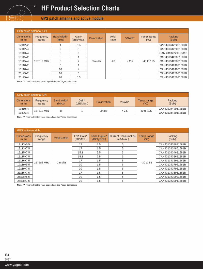
134
GPS patch antenna (CP)
Dimensions (mm)
Frequency range
Band width* (MHz)
Gain* (dBic/Max.) Polarization Axial
ratio VSWR* Temp. range (°C)
Packing (Bulk)
12x12x2
1575±2 MHz
4 -1.5
Circular < 3 < 2.5 -40 to 125
CAN4313422021581B12x12x4 9 -1 CAN4313422031581B13x13x4 6 0 CAN 4313422991581B15x15x2 5 1 CAN4313423021581B15x15x4 8 2 CAN4313423031581B18x18x2 5 1 CAN4313424021581B18x18x4 10 4 CAN4313424031581B25x25x2 10 5 CAN4313425021581B25x25x4 20 5.5 CAN4313425031581B
Note: " * " marks that the value depends on the Yageo demoboard
GPS patch antenna (LP)
Dimensions (mm)
Frequency range
Band width* (MHz)
Gain* (dBi/Max.) Polarization VSWR* Temp. range
(°C)Packing (Bulk)
15x10x41575±2 MHz 8 1 Linear < 2.5 -40 to 125
CAN4313445011581B16x06x4 CAN4313446011581B
Note: " * " marks that the value depends on the Yageo demoboard
GPS active module
Dimensions (mm)
Frequency range Polarization LNA Gain*
(dB/Max.)Noise Figure* (dB/Typical)
Current Consumption (mA/Max.)
Temp. range (°C)
Packing (Bulk)
13x13x5.5
1575±2 MHz Circular
17 1.5 5
-30 to 85
CAN4313434881581B13x13x7.5 17 1.5 5 CAN4313434861581B15x15x7.5 15.1 2.5 3 CAN4313434621581B15x15x7.5 15.1 2.5 3 CAN4313435621581B16x16x7.5 17 1.5 5 CAN4313435921581B19x19x5.5 30 1.5 6 CAN4313437951581B19x19x7.5 30 1.5 6 CAN4313437931581B21x15x7.5 17 1.5 5 CAN4313435951581B28x28x5.5 30 1.5 6 CAN4313439921581B28x28x7.5 30 1.5 6 CAN4313439911581B
Note: " * " marks that the value depends on the Yageo demoboard
HF Product Selection ChartsGPS patch antenna and active module
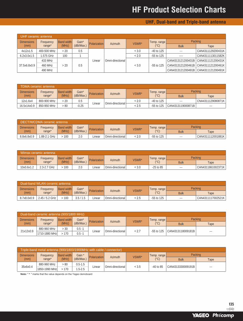
135
UHF ceramic antenna
Dimensions (mm)
Frequency range*
Band width (MHz)
Gain* (dBi/Max.) Polarization Azimuth VSWR* Temp. range
(°C)Packing
Bulk Tape 4x12x1.5 400-500 MHz > 20 0.5
Linear Omni-directional
< 3.0 -40 to 125 --- CAN4311129200431K6.2x3.0x1.5 1.575 GHz 100 1 < 2.0 -55 to 125 ---- CAN4311113011582K
37.5x6.8x0.9433 MHz
> 20 0.5 < 3.0 -55 to 125CAN4313121200431B CAN4311121200431K
460 MHz CAN4313121200461B CAN4311121200461K490 MHz CAN4313121200491B CAN4311121200491K
TDMA ceramic antenna
Dimensions (mm)
Frequency range*
Band width (MHz)
Gain* (dBi/Max.) Polarization Azimuth VSWR* Temp. range
(°C)Packing
Bulk Tape 12x1.6x4 800-900 MHz > 20 0.5
Linear Omni-directional< 2.0 -40 to 125 --- CNA4311129080871K
16.5x14x0.9 850-950 MHz > 80 -0.25 < 2.5 -55 to 125 CAN4313119000871B ---
DECT/WCDMA ceramic antenna
Dimensions (mm)
Frequency range*
Band width (MHz)
Gain* (dBi/Max.) Polarization Azimuth VSWR* Temp. range
(°C)Packing
Bulk Tape 8.8x6.8x0.9 1.88-2.1 GHz > 100 2.0 Linear Omni-directional < 2.0 -55 to 125 --- CAN4311112001881K
Wimax ceramic antenna
Dimensions (mm)
Frequency range*
Band width (MHz)
Gain* (dBi/Max.) Polarization Azimuth VSWR* Temp. range
(°C)Packing
Bulk Tape 10x0.6x1.2 2.3-2.7 GHz > 100 2.0 Linear Omni-directional < 3.0 -25 to 85 --- CAN4311861002371K
Dual-band WLAN ceramic antenna
Dimensions (mm)
Frequency range*
Band width (MHz)
Gain* (dBi/Max.) Polarization Azimuth VSWR* Temp. range
(°C)Packing
Bulk Tape 8.7x8.0x0.9 2.45 / 5.2 GHz > 100 3.5 / 1.5 Linear Omni-directional < 2.5 -55 to 125 --- CAN4311117002521K
Dual-band ceramic antenna (900/1800 MHz)
Dimensions (mm)
Frequency range*
Band width (MHz)
Gain* (dBi/Max.) Polarization Azimuth VSWR* Temp. range
(°C)Packing
Bulk Tape
21x12x0.9880-960 MHz > 30 0.5 -1
Linear Omni-directional < 2.7 -55 to 125 CAN4313118009181B ---1710-1880 MHz > 170 0.5 -1
Triple-band metal antenna (900/1800/1900MHz with cable / connector)
Dimensions (mm)
Frequency range*
Band width (MHz)
Gain * (dBi/Max.) Polarization Azimuth VSWR* Temp. range
(°C)Packing
Bulk Tape
35x6x0.4880-960 MHz > 80 0.5-1.5
Linear Omni-directional < 3.5 -40 to 85 CAN4313330009191B ---1850-1990 MHz > 170 1.5-2.5
Note: " * " marks that the value depends on the Yageo demoboard
HF Product Selection ChartsUHF, Dual-band and Triple-band antenna
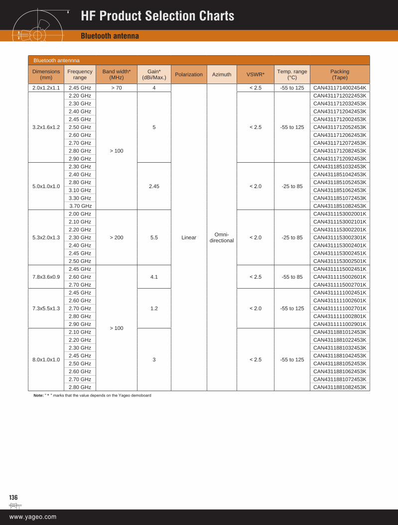
136
Bluetooth antennna
Dimensions (mm)
Frequency range
Band width* (MHz)
Gain* (dBi/Max.) Polarization Azimuth VSWR* Temp. range
(°C)Packing (Tape)
2.0x1.2x1.1 2.45 GHz > 70 4
Linear Omni- directional
< 2.5 -55 to 125 CAN4311714002454K
3.2x1.6x1.2
2.20 GHz
> 100
5 < 2.5 -55 to 125
CAN4311712022453K2.30 GHz CAN4311712032453K2.40 GHz CAN4311712042453K2.45 GHz CAN4311712002453K2.50 GHz CAN4311712052453K2.60 GHz CAN4311712062453K2.70 GHz CAN4311712072453K2.80 GHz CAN4311712082453K2.90 GHz CAN4311712092453K
5.0x1.0x1.0
2.30 GHz
2.45 < 2.0 -25 to 85
CAN4311851032453K2.40 GHz CAN4311851042453K2.80 GHz CAN4311851052453K3.10 GHz CAN4311851062453K3.30 GHz CAN4311851072453K 3.70 GHz CAN4311851082453K
5.3x2.0x1.3
2.00 GHz
> 200 5.5 < 2.0 -25 to 85
CAN4311153002001K2.10 GHz CAN4311153002101K2.20 GHz CAN4311153002201K2.30 GHz CAN4311153002301K2.40 GHz CAN4311153002401K2.45 GHz CAN4311153002451K2.50 GHz CAN4311153002501K
7.8x3.6x0.92.45 GHz
> 100
4.1 < 2.5 -55 to 85CAN4311115002451K
2.60 GHz CAN4311115002601K2.70 GHz CAN4311115002701K
7.3x5.5x1.3
2.45 GHz
1.2 < 2.0 -55 to 125
CAN4311111002451K2.60 GHz CAN4311111002601K2.70 GHz CAN4311111002701K2.80 GHz CAN4311111002801K2.90 GHz CAN4311111002901K
8.0x1.0x1.0
2.10 GHz
3 < 2.5 -55 to 125
CAN4311881012453K2.20 GHz CAN4311881022453K2.30 GHz CAN4311881032453K2.45 GHz CAN4311881042453K2.50 GHz CAN4311881052453K2.60 GHz CAN4311881062453K2.70 GHz CAN4311881072453K2.80 GHz CAN4311881082453K
Note: " * " marks that the value depends on the Yageo demoboard
HF Product Selection ChartsBluetooth antenna
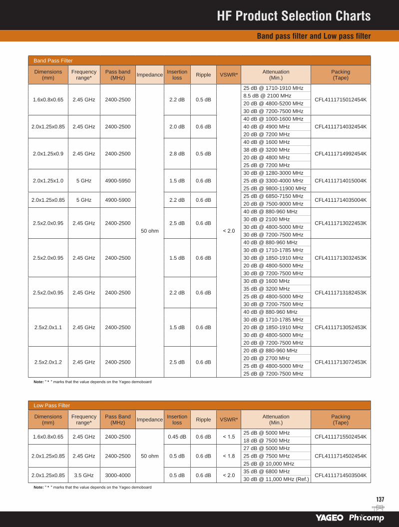
137
Band Pass Filter
Dimensions (mm)
Frequency range*
Pass band (MHz) Impedance Insertion
loss Ripple VSWR* Attenuation (Min.)
Packing (Tape)
1.6x0.8x0.65 2.45 GHz 2400-2500
50 ohm
2.2 dB 0.5 dB
< 2.0
25 dB @ 1710-1910 MHz
CFL4111715012454K8.5 dB @ 2100 MHz20 dB @ 4800-5200 MHz30 dB @ 7200-7500 MHz
2.0x1.25x0.85 2.45 GHz 2400-2500 2.0 dB 0.6 dB40 dB @ 1000-1600 MHz
CFL4111714032454K40 dB @ 4900 MHz20 dB @ 7200 MHz
2.0x1.25x0.9 2.45 GHz 2400-2500 2.8 dB 0.5 dB
40 dB @ 1600 MHz
CFL4111714992454K38 dB @ 3200 MHz20 dB @ 4800 MHz25 dB @ 7200 MHz
2.0x1.25x1.0 5 GHz 4900-5950 1.5 dB 0.6 dB30 dB @ 1280-3000 MHz
CFL4111714015004K25 dB @ 3300-4000 MHz25 dB @ 9800-11900 MHz
2.0x1.25x0.85 5 GHz 4900-5900 2.2 dB 0.6 dB25 dB @ 6850-7150 MHz
CFL4111714035004K20 dB @ 7500-9000 MHz
2.5x2.0x0.95 2.45 GHz 2400-2500 2.5 dB 0.6 dB
40 dB @ 880-960 MHz
CFL4111713022453K30 dB @ 2100 MHz30 dB @ 4800-5000 MHz30 dB @ 7200-7500 MHz
2.5x2.0x0.95 2.45 GHz 2400-2500 1.5 dB 0.6 dB
40 dB @ 880-960 MHz
CFL4111713032453K30 dB @ 1710-1785 MHz30 dB @ 1850-1910 MHz20 dB @ 4800-5000 MHz30 dB @ 7200-7500 MHz
2.5x2.0x0.95 2.45 GHz 2400-2500 2.2 dB 0.6 dB
30 dB @ 1600 MHz
CFL4111713182453K35 dB @ 3200 MHz25 dB @ 4800-5000 MHz30 dB @ 7200-7500 MHz
2.5x2.0x1.1 2.45 GHz 2400-2500 1.5 dB 0.6 dB
40 dB @ 880-960 MHz
CFL4111713052453K30 dB @ 1710-1785 MHz20 dB @ 1850-1910 MHz30 dB @ 4800-5000 MHz20 dB @ 7200-7500 MHz
2.5x2.0x1.2 2.45 GHz 2400-2500 2.5 dB 0.6 dB
20 dB @ 880-960 MHz
CFL4111713072453K20 dB @ 2700 MHz25 dB @ 4800-5000 MHz25 dB @ 7200-7500 MHz
Note: " * " marks that the value depends on the Yageo demoboard
Low Pass Filter
Dimensions (mm)
Frequency range*
Pass Band (MHz) Impedance Insertion
loss Ripple VSWR* Attenuation (Min.)
Packing (Tape)
1.6x0.8x0.65 2.45 GHz 2400-2500
50 ohm
0.45 dB 0.6 dB < 1.5 25 dB @ 5000 MHz
CFL4111715502454K18 dB @ 7500 MHz
2.0x1.25x0.85 2.45 GHz 2400-2500 0.5 dB 0.6 dB < 1.8 27 dB @ 5000 MHz
CFL4111714502454K25 dB @ 7500 MHz25 dB @ 10,000 MHz
2.0x1.25x0.85 3.5 GHz 3000-4000 0.5 dB 0.6 dB < 2.0 35 dB @ 6800 MHz
CFL4111714503504K30 dB @ 11,000 MHz (Ref.)
Note: " * " marks that the value depends on the Yageo demoboard
HF Product Selection ChartsBand pass filter and Low pass filter
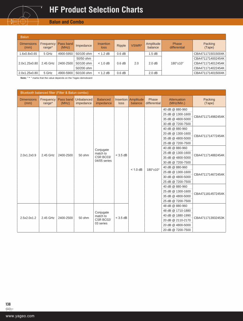
138
Balun
Dimensions (mm)
Frequency range*
Pass band (MHz) Impedance Insertion
loss Ripple VSWR* Amplitude balance
Phase differential
Packing(Tape)
1.6x0.8x0.65 5 GHz 4900-5950 50/100 ohm < 1.2 dB 0.6 dB
2.0
1.5 dB
180°±10°
CBA4711715015004K
2.0x1.25x0.80 2.45 GHz 2400-250050/50 ohm
< 1.0 dB 0.6 dB 2.0 dBCBA4711714002454K
50/100 ohm CBA4711714012454K50/200 ohm CBA4711714022454K
2.0x1.25x0.80 5 GHz 4900-5900 50/100 ohm < 1.2 dB 0.6 dB 2.0 dB CBA4711714015004K Note: " * " marks that the value depends on the Yageo demoboard
Bluetooth balanced filter (Filter & Balun combo)
Dimensions (mm)
Frequency range*
Pass band (MHz)
Unbalanced impedance
Balanced impedance
Insertion loss
Amplitude balance
Phase differential
Attenuation(MHz/Min.)
Packing(Tape)
2.0x1.2x0.9 2.45 GHz 2400-2500 50 ohm
Conjugate match to CSR BC03/04/05 series
< 3.5 dB
< 1.0 dB 180°±10°
40 dB @ 880-960
CBA4711714982454K25 dB @ 1300-160035 dB @ 4800-500030 dB @ 7200-750040 dB @ 880-960
CBA4711714772454K20 dB @ 1300-160035 dB @ 4800-500025 dB @ 7200-750040 dB @ 880-960
CBA4711714882454K25 dB @ 1300-160035 dB @ 4800-500030 dB @ 7200-750040 dB @ 880-960
CBA4711714672454K25 dB @ 1300-160030 dB @ 4800-500025 dB @ 7200-750040 dB @ 880-960
CBA4711814572454K25 dB @ 1300-160035 dB @ 4800-500025 dB @ 7200-7500
2.5x2.0x1.2 2.45 GHz 2400-2500 50 ohm
Conjugate match to CSR BC02/03 series
< 3.5 dB
48 dB @ 880-960
CBA4711713932453K
48 dB @ 1710-188040 dB @ 1880-199020 dB @ 2110-217020 dB @ 4800-500020 dB @ 7200-7500
HF Product Selection ChartsBalun and Combo
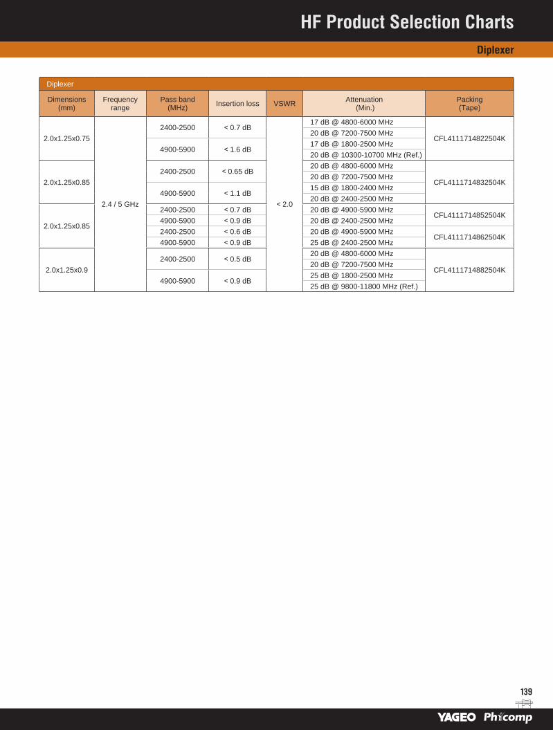
139
Diplexer
Dimensions (mm)
Frequency range
Pass band (MHz) Insertion loss VSWR Attenuation
(Min.)Packing (Tape)
2.0x1.25x0.75
2.4 / 5 GHz
2400-2500 < 0.7 dB
< 2.0
17 dB @ 4800-6000 MHz
CFL4111714822504K20 dB @ 7200-7500 MHz
4900-5900 < 1.6 dB17 dB @ 1800-2500 MHz20 dB @ 10300-10700 MHz (Ref.)
2.0x1.25x0.852400-2500 < 0.65 dB
20 dB @ 4800-6000 MHz
CFL4111714832504K20 dB @ 7200-7500 MHz
4900-5900 < 1.1 dB15 dB @ 1800-2400 MHz20 dB @ 2400-2500 MHz
2.0x1.25x0.85
2400-2500 < 0.7 dB 20 dB @ 4900-5900 MHzCFL4111714852504K
4900-5900 < 0.9 dB 20 dB @ 2400-2500 MHz2400-2500 < 0.6 dB 20 dB @ 4900-5900 MHz
CFL4111714862504K4900-5900 < 0.9 dB 25 dB @ 2400-2500 MHz
2.0x1.25x0.92400-2500 < 0.5 dB
20 dB @ 4800-6000 MHz
CFL4111714882504K20 dB @ 7200-7500 MHz
4900-5900 < 0.9 dB25 dB @ 1800-2500 MHz25 dB @ 9800-11800 MHz (Ref.)
HF Product Selection ChartsDiplexer


SMD CERAMIC EMI FILTER CAPACITORS X2Y ® PRODUCTS
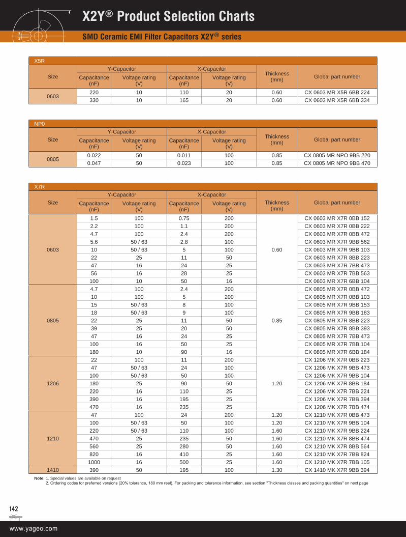
142
X5R
SizeY-Capacitor X-Capacitor
Thickness(mm) Global part numberCapacitance
(nF)Voltage rating
(V)Capacitance
(nF)Voltage rating
(V)
0603220 10 110 20 0.60 CX 0603 MR X5R 6BB 224330 10 165 20 0.60 CX 0603 MR X5R 6BB 334
NP0
SizeY-Capacitor X-Capacitor
Thickness(mm) Global part numberCapacitance
(nF)Voltage rating
(V)Capacitance
(nF)Voltage rating
(V)
08050.022 50 0.011 100 0.85 CX 0805 MR NPO 9BB 2200.047 50 0.023 100 0.85 CX 0805 MR NPO 9BB 470
X7R
SizeY-Capacitor X-Capacitor
Thickness(mm)
Global part numberCapacitance (nF)
Voltage rating (V)
Capacitance (nF)
Voltage rating (V)
0603
1.5 100 0.75 200
0.60
CX 0603 MR X7R 0BB 1522.2 100 1.1 200 CX 0603 MR X7R 0BB 2224.7 100 2.4 200 CX 0603 MR X7R 0BB 4725.6 50 / 63 2.8 100 CX 0603 MR X7R 9BB 56210 50 / 63 5 100 CX 0603 MR X7R 9BB 10322 25 11 50 CX 0603 MR X7R 8BB 22347 16 24 25 CX 0603 MR X7R 7BB 47356 16 28 25 CX 0603 MR X7R 7BB 563
100 10 50 16 CX 0603 MR X7R 6BB 104
0805
4.7 100 2.4 200
0.85
CX 0805 MR X7R 0BB 47210 100 5 200 CX 0805 MR X7R 0BB 10315 50 / 63 8 100 CX 0805 MR X7R 9BB 15318 50 / 63 9 100 CX 0805 MR X7R 9BB 18322 25 11 50 CX 0805 MR X7R 8BB 22339 25 20 50 CX 0805 MR X7R 8BB 39347 16 24 25 CX 0805 MR X7R 7BB 473
100 16 50 25 CX 0805 MR X7R 7BB 104180 10 90 16 CX 0805 MR X7R 6BB 184
1206
22 100 11 200
1.20
CX 1206 MK X7R 0BB 22347 50 / 63 24 100 CX 1206 MK X7R 9BB 473
100 50 / 63 50 100 CX 1206 MK X7R 9BB 104180 25 90 50 CX 1206 MK X7R 8BB 184220 16 110 25 CX 1206 MK X7R 7BB 224390 16 195 25 CX 1206 MK X7R 7BB 394470 16 235 25 CX 1206 MK X7R 7BB 474
1210
47 100 24 200 1.20 CX 1210 MK X7R 0BB 473100 50 / 63 50 100 1.20 CX 1210 MK X7R 9BB 104220 50 / 63 110 100 1.60 CX 1210 MK X7R 9BB 224470 25 235 50 1.60 CX 1210 MK X7R 8BB 474560 25 280 50 1.60 CX 1210 MK X7R 8BB 564820 16 410 25 1.60 CX 1210 MK X7R 7BB 824
1000 16 500 25 1.60 CX 1210 MK X7R 7BB 1051410 390 50 195 100 1.30 CX 1410 MK X7R 9BB 394
Note: 1. Special values are available on request 2. Ordering codes for preferred versions (20% tolerance, 180 mm reel). For packing and tolerance information, see section "Thickness classes and packing quantities" on next page
X2Y® Product Selection ChartsSMD Ceramic EMI Filter Capacitors X2Y® series
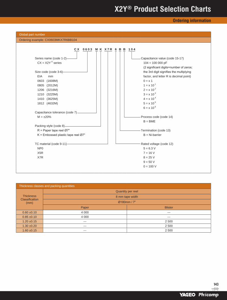
143
Global part number
Ordering example: CX0603MKX7R6BB104
C X 0 6 0 3 M K X 7 R 6 B B 1 0 4
Series name (code 1-2) Capacitance value (code 15-17)CX = X2Y ® series 104 = 100 000 pF
(2 significant digits+number of zeros; Size code (code 3-6) the 3rd digit signifies the multiplying
EIA mm factor, and letter R is decimal point)0603 (1608M) 0 = x 10805 (2012M) 1 = x 10 1
1206 (3216M) 2 = x 10 2
1210 (3225M) 3 = x 10 3
1410 (3625M) 4 = x 10 4
1812 (4632M) 5 = x 10 5
6 = x 10 6
Capacitance tolerance (code 7) M = ±20% Process code (code 14)
B = BMEPacking style (code 8)
R = Paper tape reel Ø7" Termination (code 13)K = Embossed plastic tape reel Ø7" B = Ni-barrier
TC material (code 9-11) Rated voltage (code 12)NP0 5 = 6.3 V X5R 7 = 16 VX7R 8 = 25 V
9 = 50 V 0 = 100 V
Thickness classes and packing quantities
Thickness Classification
(mm)
Quantity per reel
8 mm tape width
Ø180mm / 7”
Paper Blister0.60 ±0.10 4 000 ---0.85 ±0.10 4 000 ---1.20 ±0.15 --- 2 5001.30 ±0.20 --- 2 5001.60 ±0.15 --- 2 500
X2Y® Product Selection ChartsOrdering information


MULTILAYER CHIP VARISTORS

146
Case dimensions
T
L4
L1
L2 L3
W
Case size designation Dimensions in mm
Inch-based L1 W Tmin Tmax L2 / L3 min L2 / L3 max L4 min
0402 1.0 ±0.10 0.5 ±0.10 0.45 0.55 0.15 0.30 0.40 0603 1.6 ±0.20 0.8 ±0.10 0.70 0.90 0.20 0.60 0.40 0805 2.0 ±0.10 1.25 ±0.10 0.70 0.90 0.25 0.75 0.55 1206 3.2 ±0.15 1.6 ±0.15 0.70 0.90 0.25 0.75 1.40
Size 0402
Global part number
Varistor voltage/ Breakdown voltage
Max. continuous voltage/ Working voltage Clamping voltage Peak
current Resistance
R.T. (15 to 35°C )Capacitance @ 1 V (rms)
DC @ 1 mA D.C 8/20 µs 8/20 µs Voltage Resistance (pF) (V) (V / Max.) (V / Max.) (A) (A / Max.) (V) (MΩ / Min.) 1 KHz 1 MHz
VRS0402MR55R651N 7.2 to 10.8 5.5 14
1
30
3
1 650 390VRS0402SR55R601N 10 to 14 5.5 22 65 1 600 360VRS0402MR55R331N 7.2 to 10.8 5.5 15 30 1 330 200VRS0402MR55R201N 7.2 to 10.8 5.5 15 20 1 200 130VRS0402MR55R101N 7.2 to 10.8 5.5 15 20 1 100 60VRS0402SR55R101N 10 to 14 5.5 23 15 10 100 60VRS0402SR55R820N 10 to 14 5.5 22 10 1 82 47VRS0402SR55R680N 10 to 14 5.5 22 8 1 68 40VRS0402SR55R500N 10 to 14 5.5 23 6 10 50 30VRS0402SR55R330N 10 to 14 5.5 22 4 1 33 20VRS0402SR55R220N 10 to 14 5.5 22 2 1 22 12VRS0402SR55R100N 10 to 14 5.5 22 2 1 10 5.5VRS0402SR55R030N 50 to 80 5.5 150 2 10 3 ---VRS0402LR090201N 10.2 to 13.8 9 22 20 1 200 120VRS0402KR090101N 10.2 to 13.8 9 22 20 1 100 60VRS0402KR090500N 10.2 to 13.8 9 22 20 1 50 30VRS0402SR090500N 11 to 17 9 25 5 1 50 30VRS0402SR090330N 11 to 17 9 25 4 1 33 20VRS0402LR110181N 12.75 to 17.25 11 27 20 1 180 110VRS0402KR140161N 16.2 to 19.8 14 33 20 1 160 96VRS0402MR140161N 14.4 to 21.6 14 33 20 1 160 96VRS0402LR140161N 15.3 to 20.7 14 33 20 1 160 96VRS0402SR140121N 18 to 24 14 40 20 10 120 72VRS0402SR140101N 18 to 24 14 38 15 1 100 60VRS0402SR140500N 18 to 24 14 38 7 1 50 30VRS0402KR160121N 19.8 to 24.2 16 40 18 1 120 72VRS0402SR180121N 24 to 32 18 45 20 1 120 72VRS0402KR180900N 21.6 to 26.4 18 44 14 1 90 54VRS0402KR180820N 21.6 to 26.4 18 45 10 1 82 50VRS0402MR180500N 19.8 to 24.2 18 48 5 1 50 30VRS0402SR180500N 24 to 32 18 52 5 1 50 30VRS0402SR180400N 24 to 3s2 18 50 4 1 40 22VRS0402SR180270N 24 to 32 18 50 4 1 27 15VRS0402SR180150N 24 to 32 18 50 3 1 15 9VRS0402SR180120N 24 to 32 18 46 10 10 120 72VRS0402SR180100N 24 to 32 18 58 3 10 10 6VRS0402SR180030N 50 to 80 18 150 2 10 3 2VRS0402KR220820N 24.3 to 29.7 22 49 14 1 82 50VRS0402KR260550N 29.7 to 36.3 26 60 10 1 55 33VRS0402KR300400N 35.1 to 42.9 30 71 8 1 40 24VRS0402SR300030N 48 to 58 30 96 2 10 3 2
MLV Product Selection ChartsCase dimensions and specification for 0402
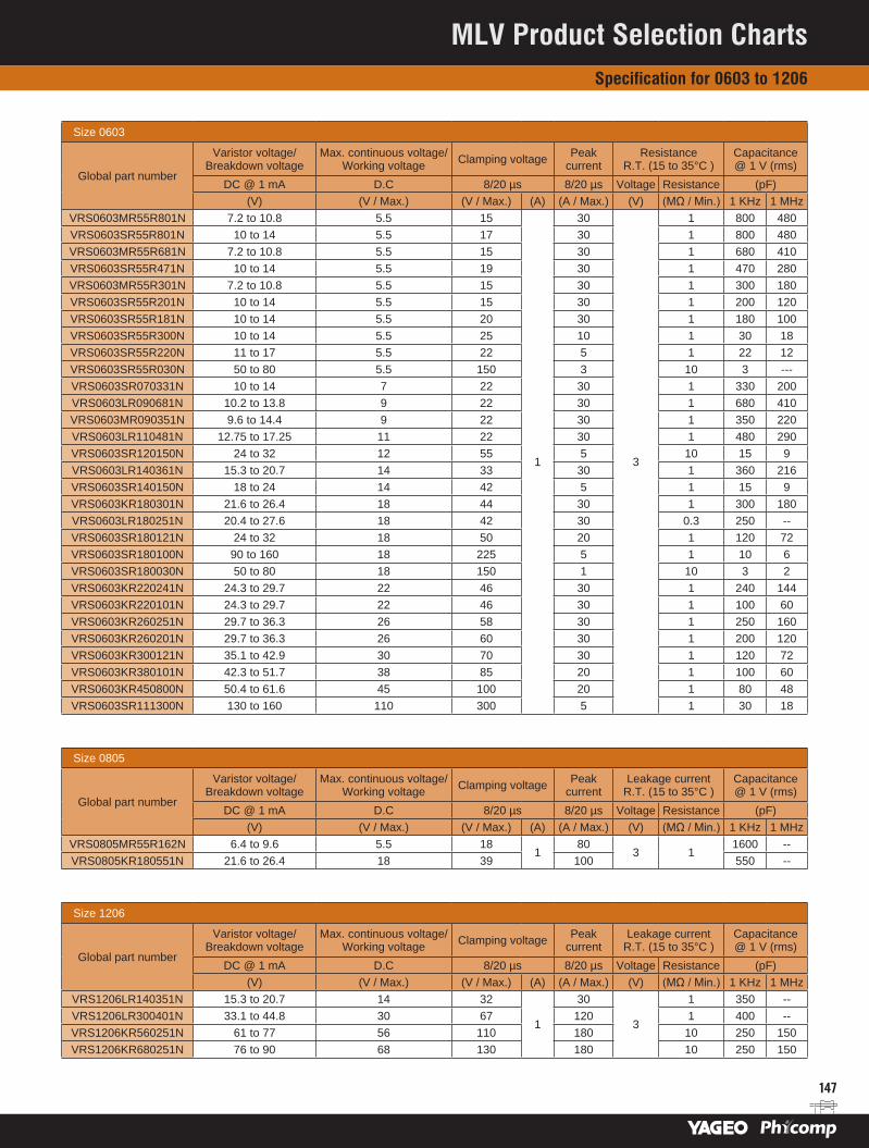
147
Size 0603
Global part number
Varistor voltage/ Breakdown voltage
Max. continuous voltage/ Working voltage Clamping voltage Peak
current Resistance
R.T. (15 to 35°C )Capacitance @ 1 V (rms)
DC @ 1 mA D.C 8/20 µs 8/20 µs Voltage Resistance (pF) (V) (V / Max.) (V / Max.) (A) (A / Max.) (V) (MΩ / Min.) 1 KHz 1 MHz
VRS0603MR55R801N 7.2 to 10.8 5.5 15
1
30
3
1 800 480VRS0603SR55R801N 10 to 14 5.5 17 30 1 800 480VRS0603MR55R681N 7.2 to 10.8 5.5 15 30 1 680 410VRS0603SR55R471N 10 to 14 5.5 19 30 1 470 280VRS0603MR55R301N 7.2 to 10.8 5.5 15 30 1 300 180VRS0603SR55R201N 10 to 14 5.5 15 30 1 200 120VRS0603SR55R181N 10 to 14 5.5 20 30 1 180 100VRS0603SR55R300N 10 to 14 5.5 25 10 1 30 18VRS0603SR55R220N 11 to 17 5.5 22 5 1 22 12VRS0603SR55R030N 50 to 80 5.5 150 3 10 3 ---VRS0603SR070331N 10 to 14 7 22 30 1 330 200VRS0603LR090681N 10.2 to 13.8 9 22 30 1 680 410VRS0603MR090351N 9.6 to 14.4 9 22 30 1 350 220VRS0603LR110481N 12.75 to 17.25 11 22 30 1 480 290VRS0603SR120150N 24 to 32 12 55 5 10 15 9VRS0603LR140361N 15.3 to 20.7 14 33 30 1 360 216VRS0603SR140150N 18 to 24 14 42 5 1 15 9VRS0603KR180301N 21.6 to 26.4 18 44 30 1 300 180VRS0603LR180251N 20.4 to 27.6 18 42 30 0.3 250 --VRS0603SR180121N 24 to 32 18 50 20 1 120 72VRS0603SR180100N 90 to 160 18 225 5 1 10 6VRS0603SR180030N 50 to 80 18 150 1 10 3 2VRS0603KR220241N 24.3 to 29.7 22 46 30 1 240 144VRS0603KR220101N 24.3 to 29.7 22 46 30 1 100 60VRS0603KR260251N 29.7 to 36.3 26 58 30 1 250 160VRS0603KR260201N 29.7 to 36.3 26 60 30 1 200 120VRS0603KR300121N 35.1 to 42.9 30 70 30 1 120 72VRS0603KR380101N 42.3 to 51.7 38 85 20 1 100 60VRS0603KR450800N 50.4 to 61.6 45 100 20 1 80 48VRS0603SR111300N 130 to 160 110 300 5 1 30 18
Size 0805
Global part number
Varistor voltage/ Breakdown voltage
Max. continuous voltage/ Working voltage Clamping voltage Peak
current Leakage current
R.T. (15 to 35°C )Capacitance @ 1 V (rms)
DC @ 1 mA D.C 8/20 µs 8/20 µs Voltage Resistance (pF) (V) (V / Max.) (V / Max.) (A) (A / Max.) (V) (MΩ / Min.) 1 KHz 1 MHz
VRS0805MR55R162N 6.4 to 9.6 5.5 181
803 1
1600 --VRS0805KR180551N 21.6 to 26.4 18 39 100 550 --
Size 1206
Global part number
Varistor voltage/ Breakdown voltage
Max. continuous voltage/ Working voltage Clamping voltage Peak
current Leakage current
R.T. (15 to 35°C )Capacitance @ 1 V (rms)
DC @ 1 mA D.C 8/20 µs 8/20 µs Voltage Resistance (pF) (V) (V / Max.) (V / Max.) (A) (A / Max.) (V) (MΩ / Min.) 1 KHz 1 MHz
VRS1206LR140351N 15.3 to 20.7 14 32
1
30
3
1 350 --VRS1206LR300401N 33.1 to 44.8 30 67 120 1 400 --VRS1206KR560251N 61 to 77 56 110 180 10 250 150VRS1206KR680251N 76 to 90 68 130 180 10 250 150
MLV Product Selection ChartsSpecification for 0603 to 1206

148
Global part number
Ordering example: VRS0402KR55R680N
V R S 0 4 0 2 K R 5 5 R 6 8 0 N
Series name (code 1-2) Process code (code 16)VR = Varistor N = Normal
Chip type (code 3) Capacitance value (code 13-15)
S = Single chip 680 = 68 pF(2 significant digits+number of zeros;
Size code (code 4-7) the 3rd digit signifies the multiplying 0402 factor, and letter R is decimal point)0603 0 = x 10805 1 = x 10 1
1206Working voltage (code 10-12)
Capacitance tolerance (code 8) 55R = 5.5 V K = ±10% 090 = 9 V L = ±15% 110 = 11 V M = ±20 % 150 = 15 V S = Special range 160 = 16 V
180 = 18 VPacking style (code 9) 220 = 22 V
R = paper tape reel Ø7 inch 260 = 26 V300 = 30 V380 = 38 V450 = 45 V560 = 56 V680 = 68 V111 = 110 V
Thickness classification and packing quantities
Type Thickness classification (mm)
8 mm tape width amount per reel180 mm / 7”
Paper0402 0.50 ±0.05 10 0000603 0.80 ±0.10 4 0000805 0.80 ±0.10 4 0001206 0.80 ±0.10 4 000
MLV Product Selection ChartsOrdering information for 0402 to 1206
Date of release: December 2008Printed in Taiwan Document order number: 2838 100 00112
© YAGEO Corporation
All rights are reserved. Reproduction in whole or in part is prohibited without the prior written consent of the copyright owner.The information presented in this document does not form part of any quotation or contract, is believed to be accurate and reliable and may be changed without notice.
No liability will be accepted by the publisher for any consequence of its use. Publication thereof does not convey nor imply any license under patent or other industrial or intellectual property rights.
For more detailed and always up-to-date contact details of sales offices, distributors and representatives, please go to our web site at
www.yageo.com
YAGEO - A GLOBAL COMPANY
ASIA
Beijing, ChinaTel. +86 10 851 20810Fax. +86 10 851 20200
Dongguan, ChinaTel. +86 769 8772 0275Fax. +86 769 8791 0053
Hong Kong, ChinaTel. +852 2342 6833Fax. +852 2342 6588
Suzhou, ChinaTel. +86 512 6825 5568Fax. +86 512 6825 5386
Tokyo, JapanTel. +81 3 5833 3331Fax. +81 3 5833 3116
Kyunggi-Do, KoreaTel. +82 31 712 4797Fax. +82 31 712 5866
Kuala Lumpur, MalaysiaTel. +60 3 8060 8864Fax. +60 3 8068 2700
SingaporeTel. +65 6244 7800Fax. +65 6244 4943
Taipei, TaiwanTel. +886 2 2917 7555Fax. +886 2 2910 9056
EUROPE
Roermond, BeneluxTel. +31 475 385 428Fax. +31 475 385 589
Brno, Czech RepublicTel. +420 7 2317 5035Fax. +420 5 4325 4936
Paris, FranceTel. +33 1 5551 8404Fax. +33 1 5551 8407
Hamburg, GermanyTel. +49 4121 870 189Fax. +49 4121 870 271
Budapest, Hungary Tel. +36 13 097 280Fax. +36 13 097 281
Milan, ItalyTel. +39 33 5140 9233Fax. +39 02 2411 3051
Moscow, Russian FederationTel. +7 916 625 92 38Fax. +7 495 374 81 87
Barcelona, SpainTel. +34 93 212 3929
Fax. +39 02 2411 3051
Croydon, UKTel. +44 208 781 1844Fax. +44 208 781 1845
NORTH AMERICA
San Jose, U.S.A. Tel. +1 408 240 6200Fax. +1 408 240 6201