PROCESSES OR APPARATUS SPECIALLY ADAPTED FOR THE ...
16
CPC - B81C - 2022.01 B81C PROCESSES OR APPARATUS SPECIALLY ADAPTED FOR THE MANUFACTURE OR TREATMENT OF MICROSTRUCTURAL DEVICES OR SYSTEMS (making microcapsules or microballoons B01J 13/02 ; processes or apparatus peculiar to the manufacture or treatment of piezo-electric, electrostrictive or magnetostrictive element per se H01L 41/22 ) Definition statement This place covers: B81C deals with manufacturing methods of microstructures as defined in the definition statement of B81B . Subject-matter belonging to B81C Documents which contain one of the following characteristics should be classified in B81C : A solution to a technical problem which is common to microstructures in general (e.g. avoiding stiction, hermetic encapsulation, fabricating structures with high aspect ratio) A process / structure which is not specific to a given application (e.g. process for making a membrane, torsion beam not specific to a given optical switch, packages for MEMS devices, machines specific to MEMS manufacturing, stamps for making microstructure). Examples: documents that deal with processes that solve a general problem but mention as an example a specific application should nevertheless be classified in B81C since the invention could also be applied to other applications Subject-matter excluded from B81C B81C doesn't cover applications which describe processes for manufacturing pure biological or chemical material (DNA sensors, carbon nanotubes ...) Processes for solving a problem which is specific to a kind of device like increasing the sensitivity of a pressure sensor Relationships with other classification places Limits with application classes (e.g. switches H01H 1/0036 ) • If the objective problem solved by the invention is related to improving physical features of the device, or realising a given function, then the document should be classified in the application classes. For example: membrane structure for improving the sensitivity of an acceleration sensor, structure for realising a bi-stable switch, structure for increasing the oscillation frequency of an RF switch. • If the objective problem solved by the invention is related to fabricating a specific or a general structure, or to a structure for solving a general problem, i.e. a problem that is not specific to a given device, then the document should be classified in B81C . For example: process for avoiding in-use stiction. Limits with Microfluidic applications Following criteria applies for classifying a document on microfluidic technology in B81C : • The document describes a method for making a microfluidic device, the function of the device being not relevant for the manufacturing process. For example, a method (e.g. bonding stamped polymer layers) for making a three dimensional arrangement of channels and grooves. 1
Transcript of PROCESSES OR APPARATUS SPECIALLY ADAPTED FOR THE ...

CPC - B81C - 2022.01
B81C
PROCESSES OR APPARATUS SPECIALLY ADAPTED FOR THEMANUFACTURE OR TREATMENT OF MICROSTRUCTURAL DEVICES ORSYSTEMS (making microcapsules or microballoons B01J 13/02; processesor apparatus peculiar to the manufacture or treatment of piezo-electric,electrostrictive or magnetostrictive element per se H01L 41/22)
Definition statement
This place covers:
B81C deals with manufacturing methods of microstructures as defined in the definition statement ofB81B.
Subject-matter belonging to B81C
Documents which contain one of the following characteristics should be classified in B81C:
A solution to a technical problem which is common to microstructures in general (e.g. avoiding stiction,hermetic encapsulation, fabricating structures with high aspect ratio)
A process / structure which is not specific to a given application (e.g. process for making a membrane,torsion beam not specific to a given optical switch, packages for MEMS devices, machines specific toMEMS manufacturing, stamps for making microstructure).
Examples:
documents that deal with processes that solve a general problem but mention as an example aspecific application should nevertheless be classified in B81C since the invention could also beapplied to other applications
Subject-matter excluded from B81C
B81C doesn't cover applications which describe processes for manufacturing pure biological orchemical material (DNA sensors, carbon nanotubes ...)
Processes for solving a problem which is specific to a kind of device like increasing the sensitivity of apressure sensor
Relationships with other classification places
Limits with application classes (e.g. switches H01H 1/0036)
• If the objective problem solved by the invention is related to improving physical features of thedevice, or realising a given function, then the document should be classified in the applicationclasses. For example: membrane structure for improving the sensitivity of an acceleration sensor,structure for realising a bi-stable switch, structure for increasing the oscillation frequency of an RFswitch.
• If the objective problem solved by the invention is related to fabricating a specific or a generalstructure, or to a structure for solving a general problem, i.e. a problem that is not specific to agiven device, then the document should be classified in B81C. For example: process for avoidingin-use stiction.
Limits with Microfluidic applications
Following criteria applies for classifying a document on microfluidic technology in B81C:
• The document describes a method for making a microfluidic device, the function of the devicebeing not relevant for the manufacturing process. For example, a method (e.g. bonding stampedpolymer layers) for making a three dimensional arrangement of channels and grooves.
1

B81C (continued)Relationships with other classification places
CPC - B81C - 2022.01
• The document describes a process which solves a technical problem general to all kind ofmicrofluidic devices
Following documents are not to be classified in B81C:
• Documents that describe a method for making a microfluidic structure which has a specificpurpose, where the structure solves a problem specific to the technical field contemplated. Forexample, a specific arrangement of channels for mixing given liquids (belongs to B01F 33/30)
• Documents which describe also a manufacturing method corresponding to a microfluidic structure,while the method is not relevant to the invention (i.e. the method doesn't contribute to solve atechnical problem general to the field of microfluidics).
• Documents that describe a process for solving a technical problem specific to the technical fieldcontemplated
Limits with Nanotechnologies (B82B)
Limit B81C vs B82B 3/00:
• Bottom-up methods for manufacturing a nanosized structure are classified in B82B
• Top-down methods for manufacturing a nanosized structure are classified in B81
• A combination of both bottom-up and top-down processes should be classified in B81 and B82B
References
Informative references
Attention is drawn to the following places, which may be of interest for search:
Actuators
Micromanipulators B25J 7/00
Ink jet, Nozzles, Production of nozzles, manufacturingprocesses, etching, dry etching, wet etching.
B41J 2/1626,B41J 2/1628,B41J 2/1629
Micropumps F04B 19/006,G01N 2035/1034
Micropumps having electric drive having plate-like flexible members, e.g.diaphragms
F04B 43/043
2

B81C (continued)Informative references
CPC - B81C - 2022.01
Mechanically-driven clocks or watches; mechanical parts of clocks orwatches in general N.B: Processes for making gears (in particular forclocks) are classified in B81C 99/0075+
G04B
Switches making use of micromechanics; Apparatus orprocesses for their manufacturing, e.g. anisotropic etching(for electrostatic relays H01H 59/0009, for relays in generalH01H 50/005)
H01H 1/0036
Electrostatic relays; Electro-adhesion relays; making use ofmicromechanics
H01H 59/0009
Piezo-electric devices (includes rotory motors, actuators and sensorsusing a piezo-electric element)
H01L 41/00
Electro active polymer (EAP) actuated artificial muscles H01L 41/00
Electrostatic motors, electric motors using thermal effect H02N 1/002, H02N 10/00
Networks comprising electromechanical or electro-acoustic devices;Electromechanical resonators. Details of microelectro-mechanicalresonators, Driving or detection means, Comb electrodes ...
H03H 9/02244, H03H 9/2405 ,H03H 9/2447
Microphones, microspeakers: Electrostatic transducers usingsemiconductor materials
H04R 19/005
3

B81C (continued)Informative references
CPC - B81C - 2022.01
Sensors
Gyroscopes; Turn-sensitive devices using gyroscopic effect, e.g.using gas, using electron beam. Turn-sensitive devices with vibratingmasses, e.g. tuning fork, the vibrating mass being an essentially two-dimensional body which undergoes a deformation or translation vibrationin a micromechanical structure
G01C 19/5719
Measuring volume flow or mass flow G01F 1/6845
IR sensor G01J 5/00
Pressure sensors, manufacturing methods of pressure sensors G01L 9/0041,G01L 9/0042
Accelerometers, Measuring acceleration; Measuring deceleration;Measuring shock, i.e. sudden change of acceleration
G01P 15/00,G01P 15/0802
Arrangements or instruments for measuring magnetic variables (flux ormagnetic sensors)
G01R 33/00
Acoustic emission sensors
Optical devices
Optical switches: Optical devices or arrangements usingmovable or deformable optical elements for controlling theintensity, colour, phase, polarisation or direction of light, e.g.switching, gating, modulating, the reflecting element being amicromechanical device, e.g. a MEMS mirror, DMD the reflectingelement being moved or deformed by electrostatic means:
by means of one or more diffracting elements: N.B: Optical devices or
arrangements using movable or deformable optical elements forcontrolling the intensity, colour, phase, polarisation or direction of light areclassified in subgroups of G02B 26/08 . In particular MEMS micromirrorsand optical devices using them for changing the direction of light aretreated in G02B 26/0833 and its subgroups.
G02B 26/0833 ,G02B 26/0841 ,G02B 26/0808
4
B81C (continued)Informative references
CPC - B81C - 2022.01
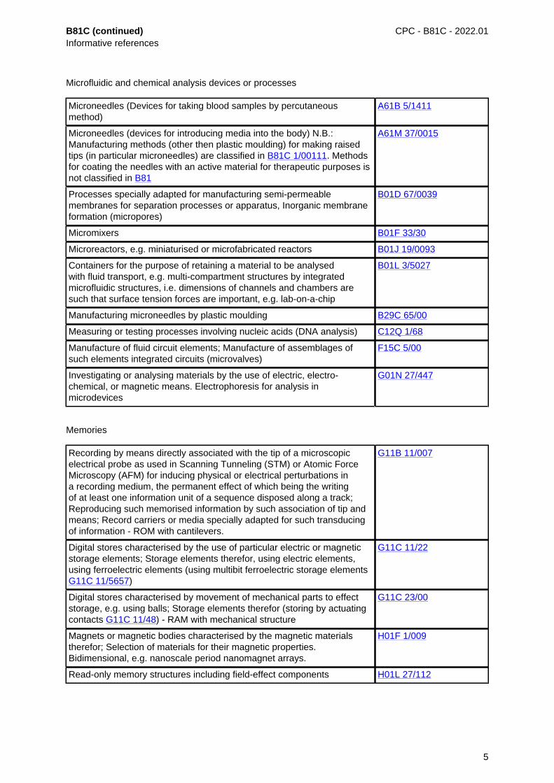
Microfluidic and chemical analysis devices or processes
Microneedles (Devices for taking blood samples by percutaneousmethod)
A61B 5/1411
Microneedles (devices for introducing media into the body) N.B.:Manufacturing methods (other then plastic moulding) for making raisedtips (in particular microneedles) are classified in B81C 1/00111. Methodsfor coating the needles with an active material for therapeutic purposes isnot classified in B81
A61M 37/0015
Processes specially adapted for manufacturing semi-permeablemembranes for separation processes or apparatus, Inorganic membraneformation (micropores)
B01D 67/0039
Micromixers B01F 33/30
Microreactors, e.g. miniaturised or microfabricated reactors B01J 19/0093
Containers for the purpose of retaining a material to be analysedwith fluid transport, e.g. multi-compartment structures by integratedmicrofluidic structures, i.e. dimensions of channels and chambers aresuch that surface tension forces are important, e.g. lab-on-a-chip
B01L 3/5027
Manufacturing microneedles by plastic moulding B29C 65/00
Measuring or testing processes involving nucleic acids (DNA analysis) C12Q 1/68
Manufacture of fluid circuit elements; Manufacture of assemblages ofsuch elements integrated circuits (microvalves)
F15C 5/00
Investigating or analysing materials by the use of electric, electro-chemical, or magnetic means. Electrophoresis for analysis inmicrodevices
G01N 27/447
Memories
Recording by means directly associated with the tip of a microscopicelectrical probe as used in Scanning Tunneling (STM) or Atomic ForceMicroscopy (AFM) for inducing physical or electrical perturbations ina recording medium, the permanent effect of which being the writingof at least one information unit of a sequence disposed along a track;Reproducing such memorised information by such association of tip andmeans; Record carriers or media specially adapted for such transducingof information - ROM with cantilevers.
G11B 11/007
Digital stores characterised by the use of particular electric or magneticstorage elements; Storage elements therefor, using electric elements,using ferroelectric elements (using multibit ferroelectric storage elementsG11C 11/5657)
G11C 11/22
Digital stores characterised by movement of mechanical parts to effectstorage, e.g. using balls; Storage elements therefor (storing by actuatingcontacts G11C 11/48) - RAM with mechanical structure
G11C 23/00
Magnets or magnetic bodies characterised by the magnetic materialstherefor; Selection of materials for their magnetic properties.Bidimensional, e.g. nanoscale period nanomagnet arrays.
H01F 1/009
Read-only memory structures including field-effect components H01L 27/112
5

B81C (continued)Informative references
CPC - B81C - 2022.01
Micromanipulators
Micromanipulators N.B: Documents which comply with the followingcriteria are to be classified in B81: The micromanipulator is specific tothe manipulation and assembling of micro- or nanoparts for MEMS orNEMS. The device solves the problem of surface forces being higherthan the gravitational force The document describes the structure andmanufacturing process of the micromanipulator. Methods for controllingthe micromanipulator are to be classified in B25J 7/00 only.
B25J 7/00
Chemistry, Nanoparticles, nanowires
Other Nanoparticles C01B 13/00, C01B 17/00,C01C, C01F
Coated nanoparticles for use as PIGMENTS and/or Fillers C01G, C09C
Hyperbranched macromolecules C08G 83/005
Nanowires - see EP0931859 - Electrolytic coating by surface reaction, i.e.forming conversion layers
C25D 11/00
Single crystal growth methods of nanorods and nanowires (deposition) C30B
Semi-conductor nanoparticles C30B
Manufacturing method for silicon nanowires / nanotubes / whiskers H01L 21/30
Nanowires as interconnects for ICs H01L 21/768
Semi-conductor nanowires / nanotubes / whiskers H01L 29/0665
Nanowires as semiconductor heterojunction of materials of differentgroups
H01L 29/267
Testing and monitoring
Measuring probes , probe needles, cantilever beams, "bump" contacts;replaceable spring loaded probe pins ; N.B: plugs, sockets or clipsare in G01R 1/0408; testing of connections in G01R 31/66; contactingIC's for test purposes when probe design is not the essential featurein G01R 31/2886; using radiation beam as probe in G01R 31/302; endpieces for wires terminating in a probe in H01R 11/18
G01R 1/06711
Testing and control, e.g. testing of apparatus components, dose control,overlay monitoring, structures for alignment control by optical means
G03F 7/70616
Details of semiconductor or other solid state devices, marks applied tosemiconductor devices (or parts), e.g. registration marks, test patterns(alignment structures, wafer maps), using circuits for characterising ormonitoring manufacturing processes, e.g. whole test die, wafers filledwith test structures, on-board-devices incorporated on each die, process/product control monitors or PCM, devices in scribe-line/kerv, drop-indevices
H01L 22/34
Apparatus for lithography
Photomechanical, e.g. photolithographic, production of textured orpatterned surfaces, e.g. printing surfaces; Materials therefor, e.g.comprising photoresists; Apparatus specially adapted therefor, Apparatusfor microlithography
G03F 2007/2067
6

B81C (continued)Informative references
CPC - B81C - 2022.01
Others
Injection moulding (for example for microneedles) B29C 45/00
Imprinting and embossing machines (EP06124007) B29C 59/00
Control arrangements or circuits, of interest only in connection withvisual indicators other than cathode-ray tubes no fixed position beingassigned to or needed to be assigned to the individual characters orpartial characters, by control of light from an independent source; Controlcircuit for an array of optical MEMS, for example for avoiding stiction, seeSA675787 -
G09G 3/34
Apparatus or processes specially adapted for manufacturing orassembling transformers, inductances, reactors or choke coils, forapplying magnetic films to substrates (covering metals, or materials withmetals, in general C23C; manufacturing record carriers G11B 5/84), forapplying nanostructures, e.g. by molecular beam epitaxy (MBE)
H01F 41/30
Variable MEMS capacitors H01G 5/16
Special rules of classification
The classification scheme in B81C comprises two kinds of classification codes:
• The codes B81C 1/00 - B81C 99/00 are the main groups which are defining technical problemssolved by the teaching of the classified documents.
• The Indexing Codes B81B 2201/00 - B81B 2207/99 and B81C 2201/00 - B81C 2900/00 aredefining technical features of the invention.
Accordingly, the classifier should stick as much as possible to the following rules:
• Each document to be classified in B81C should be allocated only one main group correspondingto the objective technical problem solved by the invention, unless the content of the documentdescribes more than one invention. In case the classification does not contain a groupcorresponding to the technical problem, the classifier should allocate either a residual group (seebelow), or in exceptional cases, when appropriate, several groups that in conjunction describe thetechnical problem.
• As the invention may comprise several essential technical features, a document classified in B81Cmay be allocated more than one Indexing Code. The Indexing Codes which are allocated shouldbe relevant to the invention.
• Furthermore, the Indexing Codes must only be allocated to documents which are receiving a maingroup
Residual Groups
The classification in B81C contains so called residual groups. For example:
B81C 1/00253 . . . Processes for integrating an electronic processing unit with a micromechanicalstructure not provided for in B81C 1/0023 - B81C 1/00246
When classifying a document which doesn't correspond to any subgroup (for exampleB81C 1/0023 - B81C 1/00246), the document must be classified in the residual group, if present, andnot in the main group. In the present example, the documents should be classified in B81C 1/00253and not in B81C 1/00222.
The classifier must stick to this policy: no new document should be classified in a main group if aresidual group is present.
The reason for these residual groups is to provide the search examiner with the certainty, that alldocuments in the groups have been classified or reclassified. If a residual group is not present, but
7

B81C (continued)Special rules of classification
CPC - B81C - 2022.01
subgroups are, the examiner has no certainty that the documents from the main group have beenreclassified when creating the subgroups.
When doing the search, the presence of the residual group indicates that all documents in the residualgroup have been classified taking into account the subgroups of the same level. Documents in thegroup of higher level, which have been split up into the sub-groups, may not have been classifiedtaking into account the sub-groups.
Therefore, at search stage, the examiner must keep in mind that he must verify if documents arepresent in the main group, since these documents have not been reclassified.
The classification structure in B81
The classification in B81, based on IPC8, makes the difference between structures and processes.In many cases, the underlying problems, which form the basis for the technical definition of a group,are solved either with a structural solution, or with a manufacturing process. Therefore, some groupdescriptors are duplicated in B81B (Structures) and in B81C (Processes).
The criteria for deciding if a document is to be classified in the structures or in the process is thefollowing:
• if the solution to the technical problem is a structure, then the document should be classified inB81B
• if the solution to the technical problem is a method, then the document belongs to B81C
Example:
B81B 3/0002 . Arrangements for avoiding sticking of the flexible or moving parts and
B81C 1/00912 . Treatments or methods for avoiding stiction of flexible or moving parts of MEMS
If for example, a document describes a process using supercritical CO2 for avoiding stiction, then itshould be classified in B81C 1/00928.
If the document describes a bump for avoiding stiction of a cantilever, then it should be classified inB81B 3/001.
Exceptions:
B81B 3/0005 contains also the processes for making anti-stiction coatings
Glossary of terms
In this place, the following terms or expressions are used with the meaning indicated:
Many technical terms in MEMS technology are defined in the SEMI norm SEMI MS3-0307. In thefollowing sections, some technical expressions are given an additional explanation in the meaning ofthe classification scheme.
Summary of static and elastic structures:
Defined by their geometry
Extending structures Pillar / ColumnTip
Depressed structures Cavity GrooveHole
Stiction Unintended adhesion of a moving part to another part
Suspended structures Bridge Cantilever Diaphragm See-saw Comb structure
8

B81C (continued)Glossary of terms
CPC - B81C - 2022.01
Defined by their function
Extending structures AnchorRib
Depressed structures ChannelNozzle
Suspended structures Flexure Membrane Spring Torsion hingeProof mass
Summary of Rotating elements
Rotating elements Gears Rack and pinionHinge
Figure 1: Basic structures
1) Cantilever 2) Bridge 3) Diaphragm 4) V-Groove 5) Well/Cavity
6) Hole/Nozzle, [1]
Pillar/Column B81B 2203/0361 A tall vertical structure, usually narrow in proportion to its height,which is usually used as a support structure, anti-adhesionstructure or a structure for thermal exchange.
Tip Tips are small pointed or rounded structures often used forScanning Probe Microscopy probes (SPM) - like atomic forcemicroscope (AFM), but also for data storage (Millipede), electrontunnelling tip (used in sensors) or microneedles.
Bump It is a raised structure similar to a tip. It is generally used todescribe the raised structures used for avoiding stiction of movableparts. It is also used in relation to structures for reducing adhesion.
Functional layers Functional layers are used mostly as protective coatings. They canprotect structures against chemical or mechanical corrosion thatcan release particles into the protected cavity. Special coatings areused also to prevent adhesion of movable structures or to reducethe stress. Metallic layers covering polymer sealing are used tomake them hermetic, but can be used also to compensate the RF-interferences.
9

B81C (continued)Glossary of terms
CPC - B81C - 2022.01
Anchor B81B 2203/0307 Anchors are structures connecting the suspended movable partsto the substrate. They can affect the resonant frequency and thereliability of the device.
Figure 2 : Anchor (US2005032266)
Rib Stiffening ribs are may be used to improve the stiffness ofsuspended structures. Improving the stiffness to mass ratio, theycan have impact on resonant frequency and efficiency of thedevices.
Cavity B81B 2203/0315 In bulk micromachining, cavity is used to make the movement of asuspended element possible. It can be used also for the protectionof movable structures in packaging, for thermal insulation or as acontainer for fluids (see Figure 1). The synonyms are chamber,hollow, well.
Groove B81B 2203/0346 A typical example is a V-Groove (see Figure 1), which canbe formed in 100 - Si substrate by KOH etching. Sometimesthe groove in 111 - Si substrate is called channel or trench todistinguish them, but we consider channel to be a function orienteddefinition. Grooves are usually used in microfluidic applications,but can also be used for precise positioning of optical fibres orcontrolled weakening of structures holding a device prior to itsseparation by breaking.
Hole B81B 2203/0353 An aperture passing through anything, a perforation, opening.
Channel B81B 2203/0338 A tube or tubular passage, natural or artificial, usually for liquids orfluids.
Nozzle A spout, mouthpiece, projecting aperture, or a short terminal pipefrom which a jet of gas or liquid may issue or be discharged (seeFigure 1).
10

B81C (continued)Glossary of terms
CPC - B81C - 2022.01
Bridge B81B 2203/0109 A bridge is a structure, erected or suspended over a surface,depression or an obstruction, connecting two or more extremities,including structures with supports deformable in torsion (seeFigure 4), flexion or supported by springs (see Figure 5 ).
Figure 3 : Bridge (flow
sensor: US6626037)
Figure 4 : Bridge with torsion hinges (accelerometer: EP1431240) Figure 5 : Bridge with
springs (inertial sensor: DE10118340) Application : thermalinsulation for flow sensors, infra-red sensors, bolometers.According to this definition, most of the accelerometers,gyroscopes and micromirrors are bridges
11

B81C (continued)Glossary of terms
CPC - B81C - 2022.01
Cantilever B81B 2203/0118 A cantilever is a structure which projects beyond a supportingcolumn on a wall and is counterbalanced and/or supported atonly one end. Cantilevers are also called flexures, suspensionor cantilever beams and suspension springs if their structure ismore complicated. These elements usually store and releasemechanical energy by deformation resulting in vibration. Aproof mass can be attached to one extremity of a cantilever.If there is a cantilever on both sides of a supported structure(proof mass or a micromirror), this structure is called abridge. Figure 6:
Cantilever/flexure with proof mass (accelerometer: EP1431240) Figure 7 : Cantilever
(microvalve: EP1496269) Application: switches, resonators,chemical and biological sensors, accelerometers
Diaphragm B81B 2203/0127 A diaphragm is a layer covering a hole or a cavity, fixed to aframe all along its periphery, separating two environments.This separation can be hermetic or not, permanent ortemporal and its opening can be controllable. Diaphragmscan be perforated or have a seismic mass attached to it.
Figure 8 :
Diaphragm (micropump: FR2862629) Applications: pressuresensors, microphones, ultra-sound resonators, valves,accelerometers, thermal insulation
12

B81C (continued)Glossary of terms
CPC - B81C - 2022.01
See-saw B81B 2203/0181 See-saw structures are suspended structures supported bya flexible element which main axis is usually perpendicularto the substrate plane. These structures can be used as asupport for micromirrors, switches, gyroscopes and resonators.
Figure 9: See-saw
(EP1306348)
Comb structure, combdrive B81B 2203/0136,B81B 2201/033
A comb is a structure with a pair of comb-shaped electrodes. Thisshape increases the total capacitor surface. Comb structuresare used for actuation or sensing. When voltage is applied, thecombs are attracted to each-other. They are often attachedto a deformable element that pulls them back to the initialposition because they can not develop a repulsive force.
Figure 10 : Comb
structure (EP1868024)
Flexure Flexure or a flexure beam is a structural element that carries loadprimarily in bending. Deformation comprises bending about anaxis normal to the beam's axis. This allows the structures to movealong the perpendicular axis to the substrate (see Figure 6).
Membrane B81B 2203/0127 A membrane is a thin layer separating two environments allowingselective mass transport control, like chemical or physical filteringor separation of substances. Membrane is often used as synonymto diaphragm.
Spring Spring is a suitably shaped structure that can return to its originalshape after a deformation (see Figure 5).
Torsion hinge Torsion hinge also called deformation hinge or a torsion beam isan element that deforms by twisting about an axis parallel to thebeam's axis. This allows the structures to rotate around the axisparallel to the substrate (see Figure 4).
Proof mass Proof mass also called seismic mass is a structural elementusually connected to a deformable element. The mass of thiselement defines the resonant frequency, sensitivity and precisionof the system. In some cases, holes or grooves are made on theproof mass to control or eliminate damping (see Figure 6).
Gears B81B 2201/035 A gear is a toothed wheel designed to transmit torque to anothergear or toothed component.
13

B81C (continued)Glossary of terms
CPC - B81C - 2022.01
Rack and pinion Structure used to transform rotation to translation movement.
Hinge The movable joint or mechanism to provide for the turning of twomovable parts. Figure
11: Hinge
Interconnects B81B 2207/07 Electrically conducting element for transmitting a signal from onepoint to another one. Interconnects that may be formed on, in orthrough the substrate or any element formed on the substrate (e.g.lid of a package). A via is a particular form of an interconnect.
Electrodes B81B 2203/04 Electrically conducting element through which an electric currententers or leaves a substance (or a vacuum) whose electricalcharacteristics are being measured, used, or manipulated. Alsoterminal points in electrical components.
Thermal actuatorsB81B 2201/031
The movement is generated by the difference in thermal expansionof two of more elements (generally beams), each elementshaving at least one anchoring point to the substrate. A typicalthermal actuator is formed out of two parallel beams (onecold beam and one thermal beam) attached at one end to thesubstrate and having one connecting point at the other end.When the temperature of the thermal beam becomes higherthan the temperature of the cold beam, the difference of thermalexpansion generates a deflection at the connecting point.
Figure 12 : Thermal
beam (US2003002133) Search and Classification Notes:Thermalactuators are also found in H01H .
14

B81C (continued)Glossary of terms
CPC - B81C - 2022.01
Bimorph and unimorph actuatorsB81B 2201/032
A bimorph is a cantilever that consists of two active layers.These layers produce a displacement via: Thermal activation (atemperature change causes one layer to expand more than theother). Electrical activation as in a piezoelectric bimorph (electricfield(s) cause one layer to extend and the other layer to contract).A piezoelectric unimorph has one active (i.e. piezoelectric) layerand one inactive (i.e. non-piezoelectric) layer. For example inthe following figure, in response to application of a voltage to thefirst movable electrode 25, the second movable electrode 26,and the third movable electrode 27, the piezoelectric thin film 1extends/contracts and the movable section 23 is driven towardthe substrate 21.
Figure 13 : Bimorph actuator (US2008296529)
B81C 1/00
Manufacture or treatment of devices or systems in or on a substrate (B81C 3/00takes precedence)
Definition statement
This place covers:
Processes for manufacturing microstructures on or in a substrate. These processes correspond to twomain processing technologies:
• Surface micromachining: techniques for making structures on a substrate by structuring layers ofmaterial added on the surface of a support substrate
• Bulk micromachining: techniques for structuring the bulk substrate
References
Limiting references
This place does not cover:
Assembling of devices or systems from individually processedcomponents
B81C 3/00
B81C 3/00
Assembling of devices or systems from individually processed components
Definition statement
This place covers:
Processes and arrangements for manufacturing microstructural devices, assembling different parts:
• Bonding parts without damaging further elements (e.g. due to high temperature)
• Aligning elements which have to be assembled
15

CPC - B81C - 2022.01
B81C 99/00
Subject matter not provided for in other groups of this subclass
Definition statement
This place covers:
Processes for manufacturing microstructural devices which are not covered by the scope of the groupsB81C 1/00 and B81C 3/00 (residual group).
In particular:
• Apparatus for manufacturing microstructural devices
• Post-processing of the microstructural devices
• Manufacturing logistics
• Processes for manufacturing substrate-free devices
References
Limiting references
This place does not cover:
Manufacture or treatment of devices or systems in or on a substrate B81C 1/00
Assembling of devices or systems from individually processedcomponents
B81C 3/00
16