
Process Independent AMS Circuit Generator Design Methodology
7
Process Independent AMS Circuit Generator Design Methodology Eric Chang UC Berkeley Berkeley, CA [email protected] Jaeduk Han UC Berkeley Berkeley, CA [email protected] Woorham Bae UC Berkeley Berkeley, CA [email protected] Zhongkai Wang UC Berkeley Berkeley, CA [email protected] Nathan Narevsky UC Berkeley Berkeley, CA [email protected] Guanghua Shu Oracle Labs Redwood Shores, CA [email protected] Frankie Liu Oracle Labs Redwood Shores, CA [email protected] Borivoje Nikolic UC Berkeley Berkeley, CA [email protected] Elad Alon UC Berkeley Berkeley, CA [email protected] Abstract—We present an update on BAG, a framework for the development of process independent Analog and Mixed Signal (AMS) circuit generators. Such generators are parametrized de- sign procedures that produce schematics, layouts, and verification testbenches for a circuit given top level specifications. We describe a universal AMS circuit verification framework built with BAG, and two new layout engines, XBase and Laygo, that enables pro- cess independent layout generation. We have developed various complex circuit generators as driving examples, including a time- interleaved SAR ADC and a SerDes transceiver frontend, taped out in TSMC 16nm FFC process. We also verify our claims of process portability by presenting layouts generated in various technology nodes, including TSMC 28nm, TSMC 16nm, TSMC 7nm, Global Foundries 45nm RF-SOI, and ST 28nm FD-SOI. I. I NTRODUCTION As Moore’s law scaling comes to a stop, circuit designers can no longer rely on new process technologies to improve the performance of their circuits; innovation in system architecture and circuit topology is necessary to design next generation systems. However, stringent and unintuitive design rules of advance multi-patterning processes [1], along with increased interconnect resistance and capacitance due to dimension scaling, severely lengthen time spent in post-layout verification and limit designers’ ability to explore new architectures and topologies. Moreover, these factors also impose a significant barrier to migrating AMS circuits to advance processes, pro- hibiting monolithic system integration and introduce perfor- mance degradation due to package/board parasitics. To address these problems, [2] introduces the Berkeley Analog Generator (BAG) framework and advocates for a generator-centric design approach. Instead of designing one circuit instance, the designer develops a circuit genera- tor, which consists of parametrized procedures that produce schematic, layout, and verification testbenches from perfor- mance specifications. With these generators, designers can easily incorporate fully automated design iteration loops on accurate post-layout simulation data in their design procedure, which can produce better circuits in less time. Furthermore, circuit generators can easily generate many circuit instances for similar applications with different specifications, which promotes design reuse and simplifies complex system design. The previously presented framework suffers from two draw- backs. First, limitations in testbench generation API prevents testbench generators from being shared between similar cir- cuits, leading to duplicated code and is prone to error. Second, layout generators are written using Synopsys’ PyCell API [3], which is not available for state-of-the-art technology nodes. Furthermore, although PyCell API provides various ”DRC correct-by-construction” functions, process portability is generally limited to process nodes with similar design rules, prohibiting development of truly process independent layout generators. In this paper, we first present a new universal verification framework for AMS circuits built on testbench generators, which can be used as a verification standard for both generated and hand-designed circuits. We then introduce two new layout generation engines, XBase and Laygo, which provide process independent layout API for designers to program layout gen- erators. Using BAG, Xbase, and Laygo, we designed a fully automatic time-interleaved SAR ADC and SerDes transceiver frontend generator, verified and taped out in TSMC 16nm. Furthermore, we demonstrate layout process portability by generating various circuit blocks in TSMC 28nm, TSMC 16nm, TSMC 7nm, Global Foundries 45nm RF SOI, and ST FD-SOI 28nm processes with no modifications necessary. The rest of the paper is organized as follows. Section II describes the universal verification framework and an up- dated generator design flow using this framework. Section III presents an overview of key principles that enables process- independent layout generation. Section IV presents the XBase layout engine, which provides various classes and functions for writing passives and analog circuits generators. Section V describes the Laygo layout engine, an alternative to XBase that operates on hand-designed layout primitives for creating compact, high-speed custom circuits. Section VI describes generators developed with these layout engines and summa- rizes our process portability results. Finally, we conclude and
Transcript of Process Independent AMS Circuit Generator Design Methodology
Process Independent AMS Circuit Generator DesignMethodology
Eric ChangUC BerkeleyBerkeley, CA
Jaeduk HanUC BerkeleyBerkeley, CA
Woorham BaeUC BerkeleyBerkeley, CA
Zhongkai WangUC BerkeleyBerkeley, CA
Nathan NarevskyUC BerkeleyBerkeley, CA
Guanghua ShuOracle Labs
Redwood Shores, [email protected]
Frankie LiuOracle Labs
Redwood Shores, [email protected]
Borivoje NikolicUC BerkeleyBerkeley, CA
Elad AlonUC BerkeleyBerkeley, CA
Abstract—We present an update on BAG, a framework for thedevelopment of process independent Analog and Mixed Signal(AMS) circuit generators. Such generators are parametrized de-sign procedures that produce schematics, layouts, and verificationtestbenches for a circuit given top level specifications. We describea universal AMS circuit verification framework built with BAG,and two new layout engines, XBase and Laygo, that enables pro-cess independent layout generation. We have developed variouscomplex circuit generators as driving examples, including a time-interleaved SAR ADC and a SerDes transceiver frontend, tapedout in TSMC 16nm FFC process. We also verify our claims ofprocess portability by presenting layouts generated in varioustechnology nodes, including TSMC 28nm, TSMC 16nm, TSMC7nm, Global Foundries 45nm RF-SOI, and ST 28nm FD-SOI.
I. INTRODUCTION
As Moore’s law scaling comes to a stop, circuit designerscan no longer rely on new process technologies to improve theperformance of their circuits; innovation in system architectureand circuit topology is necessary to design next generationsystems. However, stringent and unintuitive design rules ofadvance multi-patterning processes [1], along with increasedinterconnect resistance and capacitance due to dimensionscaling, severely lengthen time spent in post-layout verificationand limit designers’ ability to explore new architectures andtopologies. Moreover, these factors also impose a significantbarrier to migrating AMS circuits to advance processes, pro-hibiting monolithic system integration and introduce perfor-mance degradation due to package/board parasitics.
To address these problems, [2] introduces the BerkeleyAnalog Generator (BAG) framework and advocates for agenerator-centric design approach. Instead of designing onecircuit instance, the designer develops a circuit genera-tor, which consists of parametrized procedures that produceschematic, layout, and verification testbenches from perfor-mance specifications. With these generators, designers caneasily incorporate fully automated design iteration loops onaccurate post-layout simulation data in their design procedure,which can produce better circuits in less time. Furthermore,circuit generators can easily generate many circuit instances
for similar applications with different specifications, whichpromotes design reuse and simplifies complex system design.
The previously presented framework suffers from two draw-backs. First, limitations in testbench generation API preventstestbench generators from being shared between similar cir-cuits, leading to duplicated code and is prone to error. Second,layout generators are written using Synopsys’ PyCell API[3], which is not available for state-of-the-art technologynodes. Furthermore, although PyCell API provides various”DRC correct-by-construction” functions, process portabilityis generally limited to process nodes with similar design rules,prohibiting development of truly process independent layoutgenerators.
In this paper, we first present a new universal verificationframework for AMS circuits built on testbench generators,which can be used as a verification standard for both generatedand hand-designed circuits. We then introduce two new layoutgeneration engines, XBase and Laygo, which provide processindependent layout API for designers to program layout gen-erators. Using BAG, Xbase, and Laygo, we designed a fullyautomatic time-interleaved SAR ADC and SerDes transceiverfrontend generator, verified and taped out in TSMC 16nm.Furthermore, we demonstrate layout process portability bygenerating various circuit blocks in TSMC 28nm, TSMC16nm, TSMC 7nm, Global Foundries 45nm RF SOI, and STFD-SOI 28nm processes with no modifications necessary.
The rest of the paper is organized as follows. Section IIdescribes the universal verification framework and an up-dated generator design flow using this framework. Section IIIpresents an overview of key principles that enables process-independent layout generation. Section IV presents the XBaselayout engine, which provides various classes and functionsfor writing passives and analog circuits generators. Section Vdescribes the Laygo layout engine, an alternative to XBasethat operates on hand-designed layout primitives for creatingcompact, high-speed custom circuits. Section VI describesgenerators developed with these layout engines and summa-rizes our process portability results. Finally, we conclude and
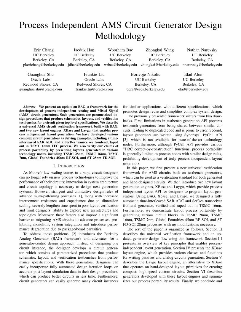
(a) Generator interface UML diagram(b) Generated differential amplifier instance
(c) Differential amplifier DUT wrapper for step response testbench (d) Transient testbench with step input.
Fig. 1: Generator interface example
discuss future work in Section VII.
II. UNIVERSAL VERIFICATION FRAMEWORK
Due to limitations in the testbench generation API, the BAGframework presented in [2] requires each testbench generatorto be associated to a specific circuit. This results in much codebeing duplicated when the same testbench needs to be usedfor different circuit topologies, which is prone to error anddifficult to maintain.
To address this issue, we made several improvements on thetestbench generation API that separate testbench generationfrom circuit generation and enable testbench reuse. Withthis new capability, we constructed a verification frameworkfor AMS circuits, shown in lower part of Figure 1a. Thisframework consists of testbench generators and associatedsimulation data post-processing routines, which can be used tocharacterize any type of circuit. A circuit generator will thenuse the verification framework on generated circuits to obtainperformance results.
We demonstrate the new generator flow using a simpledifferential amplifier, with schematic shown in Figure 1b.The circuit generator determines component parameters fromtop level specifications using design equations and generatesthe schematic and layout instances. At the same time, thecircuit generator also generates a device-under-test (DUT)wrapper schematic for each testbench, with one shown in
Figure 1c. The DUT wrapper serves two main purposes.First, it transforms the DUT input/output pin interface to astandard interface defined by the testbench. In this case, itinstantiates two ideal baluns to perform differential-to-single-ended conversions, and adds various bias voltage sources.Second, it provides proper loading to the DUT, which canbe capacitors, resistors, or even other circuit instances.
To measure the settling time of this circuit, the circuitgenerator invokes the settling time measurement procedure inthe verification framework, which generates a step responsetestbench using the given DUT wrapper, shown in Figure 1d.This testbench provides a step response on the input “in” andmeasures the settling time on output “out”, with additionaloutputs available for debugging purposes (“outcm” in thisexample). The verification procedure simulates this testbenchand reports the settling time back to the circuit generator. Otherperformance metric such as gain, bandwidth, power supplyrejection ratio (PSRR), and so on can be obtained in the sameway.
With this new approach, an universal verification standardcan be defined for all analog circuits. Complex verificationprocedures simply need to be programmed once by experi-enced designers and can be applied to all circuits. Incidentally,since the verification framework acts on generated circuitinstances, it can be easily configured to verify hand-designed

Fig. 2: XBase top level UML diagram.
custom circuits. This makes verification an easy first step forincremental adoption of generator based methodology.
In the rest of the paper, we focus on our new layout gen-eration API, which enables the development of truly processindependent circuit generators.
III. PROCESS PORTABLE LAYOUT
Fig. 3: Typical amplifier floor plan.
There are two key insights behind our solution for process-portable layout generators. First, despite vast differences inthe device geometry and design rules, The layout floor planfor a circuit with a given application is almost always thesame. Figure 3 shows a typical floor plan for an amplifiercircuit. By using vertical wires to connect between transistorand substrate rows, the number of wires naturally scales withnumber of fingers, thus minimizing interconnect resistance andmaximizing transistor current density limit due to electromi-gration constraints. Therefore, by constructing a layout APIthat allows designers to draw various common floor plansand abstract away geometry details of the underlying devices,generators written in this API would be process portable.
Second, complex and unintuitive multi-patterning designrules have driven circuit designers to enforce regular routing
grids even in custom layouts. Therefore, by enforcing a routinggrid system where both the width and spacing of the wires arequantized, and wires on the same layer must travel in the samedirection (with adjacent layers having alternating directions),we can ensure DRC correctness by simply adjusting therouting grid parameters. Most importantly, layout generatorswritten to draw all wires on routing grid can be easily portedacross different process nodes.
In the next two sections, we present two layout engines thatimplement these concepts.
IV. XBASE OVERVIEW
The top level UML diagram for XBase is shown in Figure 2.Python abstract base classes are used to encapsulate commonlayout methods and separate process independent generatorsfrom process specific primitives.TemplateBase is the fundamental class that all layout
generators are based on. It defines two sets of APIs, onehigh level and one low level, that designers call to createlayout geometries. the low level API contains methods suchas add_rect() and add_via(), which draw any prim-itive geometries with no restrictions. These methods do notguarantee DRC correctness and therefore are mostly used inprimitive implementations. The high level API contains meth-ods such as connect_to_track(), which create wireson the routing grid described by the RoutingGrid class.Layout generators written solely using methods in the highlevel API will be process portable. Finally, TemplateBasedefines an abstract method called draw_layout(), whichmust be implemented by its subclasses to create layout for thespecific circuits.
Each different type of layout floor plan is implemented as anabstract subclass of TemplateBase, which provide methodsfor drawing the specific floor plan. AnalogBase is an ab-stract class specialized in drawing layout floor plan for electro-migration rules constrained analog circuits, as describedin Section III. AnalogBase provides the draw_base()

method, which draws rows of transistors and substrate tapsbased on user supplied parameters, such as number of fingersper row, number of rows, number of horizontal routing tracksper row, and so on. It also defines methods that connecttransistors and substrate taps to the routing grid. To createan amplifier generator with this floor plan (represented byAmplifier class in Figure 2), designers simply sub-classAnalogBase and implement the draw_layout() methodby calling draw_base() and other related methods withproper parameters.
To enable process portability, abstract primitive classes areused to separate process specific layouts from AnalogBase.These primitive classes define abstract methods that encap-sulates all design rules relevant to the floor plan it supports.Methods in AnalogBase such as draw_base() call thesefunctions and determine how to correctly assemble the primi-tives together. As the result, by simply changing routing gridparameters and implementations of these abstract primitiveclasses, the designer can generate circuits in another processtechnology using the same layout generator.
In addition to AnalogBase, XBase also provides aResArrayBase for drawing resistor arrays. With these twoclasses, many analog circuit generators can be written.
V. LAYGO OVERVIEW
Laygo stands for LAYout with Gridded Objects, and asthe name implies, it is developed for generating DRC clean-by-construction layouts by placing layout elements on gridsand utilizing relative and symbolic information, rather thanphysical numbers. The main difference of Laygo from XBaseis that Laygo uses manually designed, process-specific layoutprimitives for encapsulating design rules, while XBase usesabstract base classes.
Figure 4 shows the structure of Laygo framework.GridLayoutGenerator is the main class for layout gen-erations. Users create various layout geometries by call-ing functions defined in GridLayoutGenerator, such asrelplace() (for instance placements), route() (for wireroutings), and via() (for via placements).
Fig. 4: Laygo Structure
The relplace() function places instances (whosegeneric information are stored in the TemplateDB object)
based on integer grid coordinates on placement grid and rel-ative information with neighboring structures (ref parameterin Figure 5(a)). The GridDB object stores the placementgrid information (x, y resolution) for the placement operation.Since the relplace() function uses abstract grid or relativeinformation between instances, the process portability is guar-anteed if all primitive templates are designed to be alignedwith the process-specific placement grids. The route()function draws routing patterns on predefined routing grids.Similar to the relplace() function, in order to createwires without dealing with physical coordinates, the route()receives integer coordinates on abstract routing grids or targetobjects to connect the routing wire (Figure 5(b)). All integerrouting coordinates are converted to physical coordinates bycombining the integer values and routing grid information(pitches, widths). The via() function places via objects,using a similar method with the aforementioned functions(Figure 5(c)).
Fig. 5: Laygo generation example (a) relplace (b) route (c) via
The three place and route functions compose the coregenerator flow, while high-level functions that construct morecomplex geometries (by combining the core functions) areprovided as well. It should be noted that any non-uniform gridsin terms of pitch and routing width can be used for placementand routes (as shown in Figure 5), which yields high quality-of-results (by optimizing the grid values for given technology),while still abstracting design rules.
All layout structures are stored in LayoutDB and exportedto LayoutIO, to create the final layout in OpenAccess orGDS format.
(a) transmitter frontend (b) receiver frontend
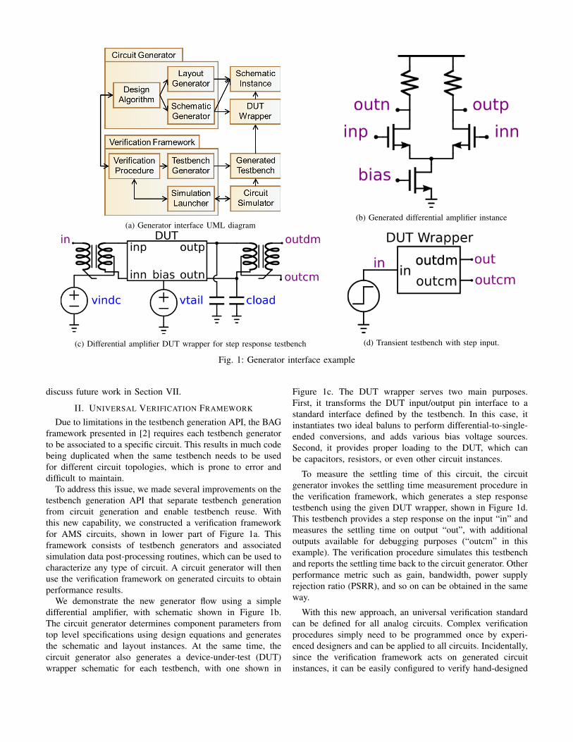
Fig. 6: SerDes frontend layout photo
(a) TISAR ADC in TSMC 16nm (b) TISAR ADC core in ST FDSOI 28nm
Fig. 7: TISAR ADC layout photo
VI. RESULTS
To demonstrate the effectiveness of BAG, we designed aSerDes frontend layout generator using XBase (Figure 6)and taped out in TSMC 16nm FFC process. The SerDestransceiver is designed for 20 Gb/s, the receiver datapathemploys the dynamic latch and charge integration topology[4], and contains a passive CTLE, 1 tap FFE, and a 3 tap DFE.All transistor sizes and the number of DFE taps in the SerDesfrontend are programmable. The Serdes frontend occupies anarea of 195µm by 110µm, including AC coupling capacitorsand ESD diodes.
We also developed a time-interleaved SAR ADC generatorusing both XBase and Laygo (Figure 7). The ADC top levelspecifications are all programmable, and an instance targeting9.6 GS/s with 8-way interleaving, 6 bits of ENOB with 9physical output bits is taped out in TSMC 16nm. The totalarea of the entire ADC is 500µm by 100µm.
We also present layout generators written in XBase for LDOregulator and MOS/MOM decoupling capacitor, with layoutinstances generated in TSMC 7nm, shown in Figure 8. Theseblocks are used in an injection-locked ring oscillator PLL andthe generated layouts are DRC clean with no modificationsneeded. These results further prove that our layout generationframework is capable of handling latest technology nodes.
To validate our claim of process portability, we ran our
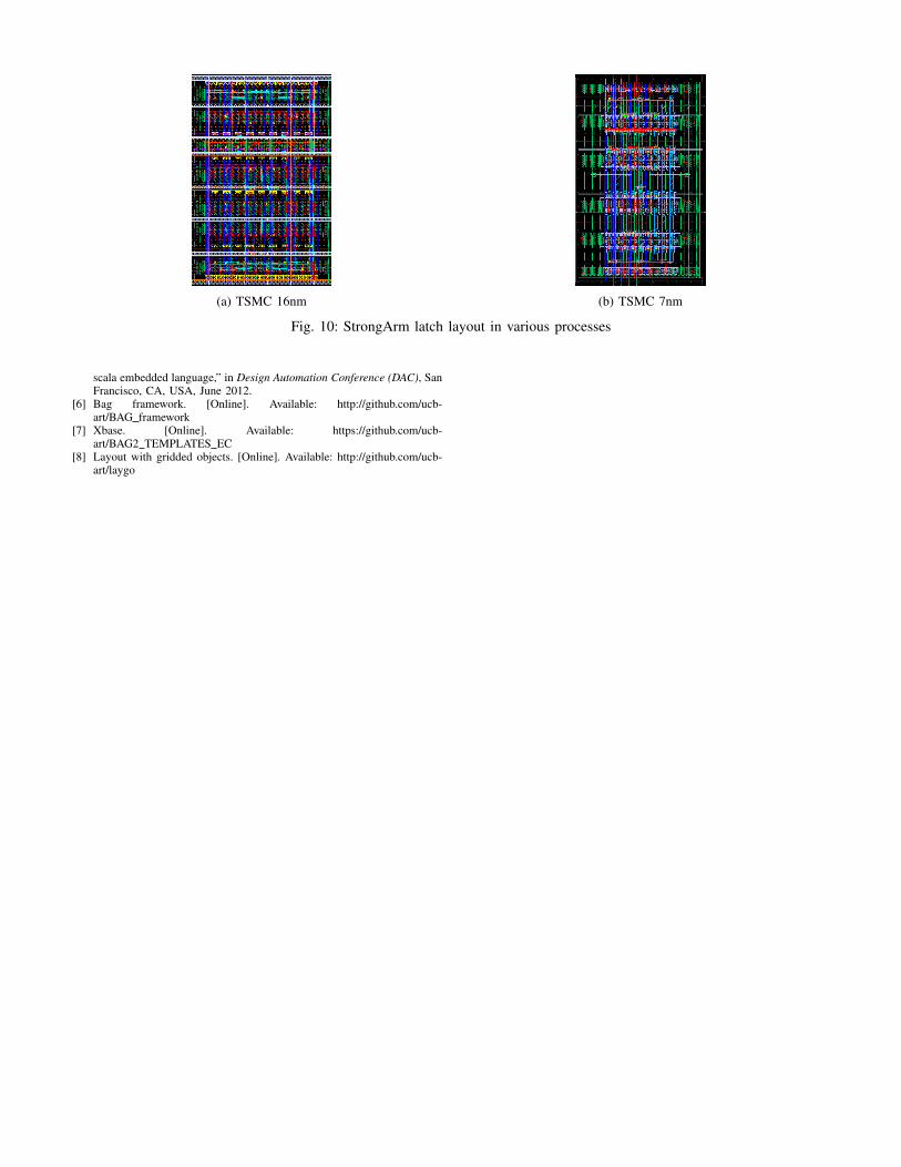
layout generators on various process technologies with onlychanges in primitive implementations. For Laygo, we regen-erated the ADC core in ST FDSOI 28nm, which consistsof sense amplifier, capacitor bank, and SAR logic, shown inFigure 7b. For XBase, we generated differential amplifiers andStrongArm latches in Global Foundaries RF SOI 45nm, TSMC28nm, TSMC 16nm, and TSMC 7nm, shown in Figure 9 andFigure 10, respectively. Despite the vast differences in designrules, all generated layouts and schematics are DRC and LVSclean.
VII. CONCLUSION
A substantial change in AMS circuit design and verificationflow is necessary to continue innovation beyond Moore’s lawscaling. We described a new universal verification frame-work built with testbench generators, which helps define averification standard for AMS circuits. We then presentedtwo new layout generator framework, XBase and Laygo, thatenables development of process independent circuit generatorseven with advance technology nodes. To prove our claim,we designed various complex generators and taped out inTSMC 16nm FFC process, including a SerDes frontend and atime-interleaved SAR ADC. We further demonstrate processportability by running our generators in a variety of technologynodes.

(a) LDO regulator in TSMC 7nm
(b) MOS/MOM decoupling capcitors in TSMC 7nm
Fig. 8: Various layouts in TSMC 7nm
(a) Global Foundaries 45nm RF SOI (b) TSMC 28nm (c) TSMC 16nm
Fig. 9: Differential amplifier layout in various processes
We have shown that generator based design methodology isa viable path to AMS circuit design automation. As futurework, we plan to explore development of complete SOCgenerators by integrating BAG with digital synthesis toolsand other high level hardware construction languages, suchas Chisel [5]. BAG [6], XBase [7], and Laygo [8] are releasedunder open source licenses, and documentations/tutorials arecurrently under active development.
ACKNOWLEDGMENT
This research was supported by DARPA under the CRAFTprogram. The authors acknowledge Oracle Labs for supportingdevelopment in TSMC 7nm.
REFERENCES
[1] M. White. (2017, Jan.) Are you (really) ready for your next node?[Online]. Available: http://www.electronicdesign.com/eda/are-you-really-ready-your-next-node
[2] J. Crossley, A. Puggelli, H.-P. Le, B. Yang, R. Nancollas, K. Jung,L. Kong, N. Narevsky, Y. Lu, N. Sutardja, E. J. An, A. L. Sangiovanni-Vincentelli, and E. Alon, “Bag: A designer-oriented integrated frameworkfor the development of ams circuit generators,” in IEEE/ACM Interna-tional Conference on Computer-Aided Design (ICCAD). San Jose, CA,USA: IEEE, Nov. 2013, pp. 74–81.
[3] S. Alassi and B. Winter, “Pycells for an open semiconductorindustry,” CoRR, vol. abs/1607.00859, 2016. [Online]. Available:http://arxiv.org/abs/1607.00859
[4] J. Han, Y. Lu, N. Sutardja, K. Jung, and E. Alon, “Design techniques fora 60 gb/s 173 mw wireline receiver frontend in 65 nm cmos technology,”IEEE Journal of Solid-State Circuits, vol. 51, no. 4, pp. 871–880, April2016.
[5] J. Bachrach, H. Vo, B. Richards, Y. Lee, A. Waterman, R. Avizienis,J. Wawrzynek, and K. Asanovic, “Chisel: Constructing hardware in a
(a) TSMC 16nm (b) TSMC 7nm
Fig. 10: StrongArm latch layout in various processes
scala embedded language,” in Design Automation Conference (DAC), SanFrancisco, CA, USA, June 2012.
[6] Bag framework. [Online]. Available: http://github.com/ucb-art/BAG framework
[7] Xbase. [Online]. Available: https://github.com/ucb-art/BAG2 TEMPLATES EC
[8] Layout with gridded objects. [Online]. Available: http://github.com/ucb-art/laygo