Probing Flow Velocity with Silicon Nanowire Sensors · PDF fileProbing Flow Velocity with...
5
Probing Flow Velocity with Silicon Nanowire Sensors Dong Rip Kim, Chi Hwan Lee, and Xiaolin Zheng* Department of Mechanical Engineering, Stanford UniVersity, California 94305 Received January 22, 2009; Revised Manuscript Received March 5, 2009 ABSTRACT We report our experimental efforts to quantify the impact of fluidic and ionic transport on the conductance level of silicon nanowire (SiNW) sensors configured as field effect transistors (FETs). Specifically, the conductance of SiNW FETs placed in a microfluidic channel was observed to change linearly with the flow velocity of electrolytic solutions. The direction of conductance change depends on the doping type of the SiNWs and their location inside the microfluidic channel, and the magnitude of the conductance change varies with the ionic strength and compositions of the electrolytic solution. Our quantitative analysis suggests that the flow velocity sensing is a consequence of the streaming potential that is generated by the movement of counterions inside the electrical double layer (EDL) of the silica substrate. The streaming potential, which varies with the flow velocity and the ionic properties of the electrolytic solution, acts in the same way as the charged analytes in affecting the conductance of SiNWs by changing the surface potential. This study highlights the importance of considering the ionic transport in analyzing and optimizing nanowire FET sensors, which can significantly change the conductance of NWs. Moreover, SiNWs were demonstrated for the first time to be able to detect the streaming potential, the flow velocity and the ionic strength, opening up their new application potentials in microfluidics. Semiconducting NWs configured as FETs have recently attracted considerable attention because of their great po- tential as label-free, real-time, and ultrasensitive biological and chemical sensors. 1-7 In particular, SiNWs were success- fully demonstrated to possess great selectivity in detecting a wide range of charged species, such as proteins, viruses, and DNAs. 1-7 The NW sensors typically operate in an electrolytic solution and respond to changes in the local electric potential caused by the specific binding and unbind- ing events between the receptors and the target molecules. 8 However, in the sensing environment, the charged analytes coexist with charged ions of the electrolytic solution and the variation in the ionic distribution in the vicinity of the NW sensors can also affect the local electric potential around the NWs. This will lead to a conductance change of the NWs, which may overshadow the signals from the specific binding events and impact the selectivity of NW FET sensors. The effects of the ionic distribution on the electric potential inside an aqueous solution have been recognized and utilized as the detection mechanism for the ion-sensitive field effect transistor (ISFET). Nonetheless, the electric properties of ions have frequently been neglected for simplicity when analyzing NW FET sensors by assuming the electrolytic solution to be charge neutral. 9-11 Therefore, it is important to investigate the impact of charged ions on the conductance level of NW FET sensors so that the performance of NW sensors can be further improved. To understand the physics underlying the influence of ions on NW FET sensors, we have undertaken and report herein experimental efforts to quantify the impact of ions on the conductance level of SiNW FET sensors. Our experimental results indicate that the ionic distribution and the transport of the electrolytic solution can significantly affect the conductance level of SiNW FET sensors and that the interaction mechanism is closely related to the streaming potential generated by the streamwise ionic movement. Moreover, the effects of ions on SiNWs can be utilized to develop SiNW sensors to measure the flow velocity of the solution and to probe the properties of the solution. The SiNWs were configured as FETs to detect flow velocity. The experimental setup is similar to previously reported SiNW FET sensing experiments, 8 as shown in Figure 1a, where SiNWs are located on the floor of the microfluidic channel. The channel consists of a Si/SiO 2 floor and a cover made from the polydimethylsiloxane (PDMS). Differently from some previous NW FET sensing experi- ments, 8 an Ag/AgCl reference electrode was placed in the center of the channel to fix the local electric potential of the solution and hence to reduce the noise generated by the drifting of the solution potential. 12-14 The SiNWs were synthesized using the vapor-liquid-solid mechanism with 20 nm gold nanoclusters, at a 4000:1 Si/B feeding ratio for the p-type and a 2000:1 Si/P feeding ratio for the n-type SiNWs, respectively. 15-17 Arrays of SiNW sensors were fabricated using photolithography with Ti/Pd as the source and drain metal contacts. 8,18 These contacts were further * Corresponding author. E-mail: [email protected]. NANO LETTERS 2009 Vol. 9, No. 5 1984-1988 10.1021/nl900238a CCC: $40.75 2009 American Chemical Society Published on Web 03/30/2009 Downloaded by PURDUE UNIV on September 9, 2015 | http://pubs.acs.org Publication Date (Web): March 30, 2009 | doi: 10.1021/nl900238a
Transcript of Probing Flow Velocity with Silicon Nanowire Sensors · PDF fileProbing Flow Velocity with...

Probing Flow Velocity with SiliconNanowire SensorsDong Rip Kim, Chi Hwan Lee, and Xiaolin Zheng*
Department of Mechanical Engineering, Stanford UniVersity, California 94305
Received January 22, 2009; Revised Manuscript Received March 5, 2009
ABSTRACT
We report our experimental efforts to quantify the impact of fluidic and ionic transport on the conductance level of silicon nanowire (SiNW)sensors configured as field effect transistors (FETs). Specifically, the conductance of SiNW FETs placed in a microfluidic channel was observedto change linearly with the flow velocity of electrolytic solutions. The direction of conductance change depends on the doping type of theSiNWs and their location inside the microfluidic channel, and the magnitude of the conductance change varies with the ionic strength andcompositions of the electrolytic solution. Our quantitative analysis suggests that the flow velocity sensing is a consequence of the streamingpotential that is generated by the movement of counterions inside the electrical double layer (EDL) of the silica substrate. The streamingpotential, which varies with the flow velocity and the ionic properties of the electrolytic solution, acts in the same way as the charged analytesin affecting the conductance of SiNWs by changing the surface potential. This study highlights the importance of considering the ionictransport in analyzing and optimizing nanowire FET sensors, which can significantly change the conductance of NWs. Moreover, SiNWs weredemonstrated for the first time to be able to detect the streaming potential, the flow velocity and the ionic strength, opening up their newapplication potentials in microfluidics.
Semiconducting NWs configured as FETs have recentlyattracted considerable attention because of their great po-tential as label-free, real-time, and ultrasensitive biologicaland chemical sensors.1-7 In particular, SiNWs were success-fully demonstrated to possess great selectivity in detectinga wide range of charged species, such as proteins, viruses,and DNAs.1-7 The NW sensors typically operate in anelectrolytic solution and respond to changes in the localelectric potential caused by the specific binding and unbind-ing events between the receptors and the target molecules.8
However, in the sensing environment, the charged analytescoexist with charged ions of the electrolytic solution and thevariation in the ionic distribution in the vicinity of the NWsensors can also affect the local electric potential around theNWs. This will lead to a conductance change of the NWs,which may overshadow the signals from the specific bindingevents and impact the selectivity of NW FET sensors. Theeffects of the ionic distribution on the electric potential insidean aqueous solution have been recognized and utilized asthe detection mechanism for the ion-sensitive field effecttransistor (ISFET). Nonetheless, the electric properties of ionshave frequently been neglected for simplicity when analyzingNW FET sensors by assuming the electrolytic solution tobe charge neutral.9-11 Therefore, it is important to investigatethe impact of charged ions on the conductance level of NWFET sensors so that the performance of NW sensors can befurther improved.
To understand the physics underlying the influence of ionson NW FET sensors, we have undertaken and report hereinexperimental efforts to quantify the impact of ions on theconductance level of SiNW FET sensors. Our experimentalresults indicate that the ionic distribution and the transportof the electrolytic solution can significantly affect theconductance level of SiNW FET sensors and that theinteraction mechanism is closely related to the streamingpotential generated by the streamwise ionic movement.Moreover, the effects of ions on SiNWs can be utilized todevelop SiNW sensors to measure the flow velocity of thesolution and to probe the properties of the solution.
The SiNWs were configured as FETs to detect flowvelocity. The experimental setup is similar to previouslyreported SiNW FET sensing experiments,8 as shown inFigure 1a, where SiNWs are located on the floor of themicrofluidic channel. The channel consists of a Si/SiO2 floorand a cover made from the polydimethylsiloxane (PDMS).Differently from some previous NW FET sensing experi-ments,8 an Ag/AgCl reference electrode was placed in thecenter of the channel to fix the local electric potential ofthe solution and hence to reduce the noise generated by thedrifting of the solution potential.12-14 The SiNWs weresynthesized using the vapor-liquid-solid mechanism with20 nm gold nanoclusters, at a 4000:1 Si/B feeding ratio forthe p-type and a 2000:1 Si/P feeding ratio for the n-typeSiNWs, respectively.15-17 Arrays of SiNW sensors werefabricated using photolithography with Ti/Pd as the sourceand drain metal contacts.8,18 These contacts were further* Corresponding author. E-mail: [email protected].
NANOLETTERS
2009Vol. 9, No. 51984-1988
10.1021/nl900238a CCC: $40.75 2009 American Chemical SocietyPublished on Web 03/30/2009
Dow
nloa
ded
by P
UR
DU
E U
NIV
on
Sept
embe
r 9,
201
5 | h
ttp://
pubs
.acs
.org
P
ublic
atio
n D
ate
(Web
): M
arch
30,
200
9 | d
oi: 1
0.10
21/n
l900
238a
passivated with SU-8 to prevent the leakage of current intothe electrolytic solution. The SU-8 passivation quality wasexcellent because devices did not exhibit any noticeabledegradation over 1 week of sensing experiments. Theconductance of SiNWs was measured using lock-in detectionby applying a 30mV voltage with a frequency of a few kHzand measuring the current.8 The electrolytic solutions usedin this study were potassium chloride in potassium phosphatebuffers, unless mentioned otherwise. The pH value of thesolution was 7, achieved by mixing the monobasic (KH2PO4)and dibasic (K2HPO4) potassium phosphates in DI water.The ionic strength of the solution was controlled by dilutingthe solution with DI water and adding potassium chloride(KCl). The flow velocity of the solution inside the microf-luidic channel was controlled by a syringe pump (HarvardApparatus).
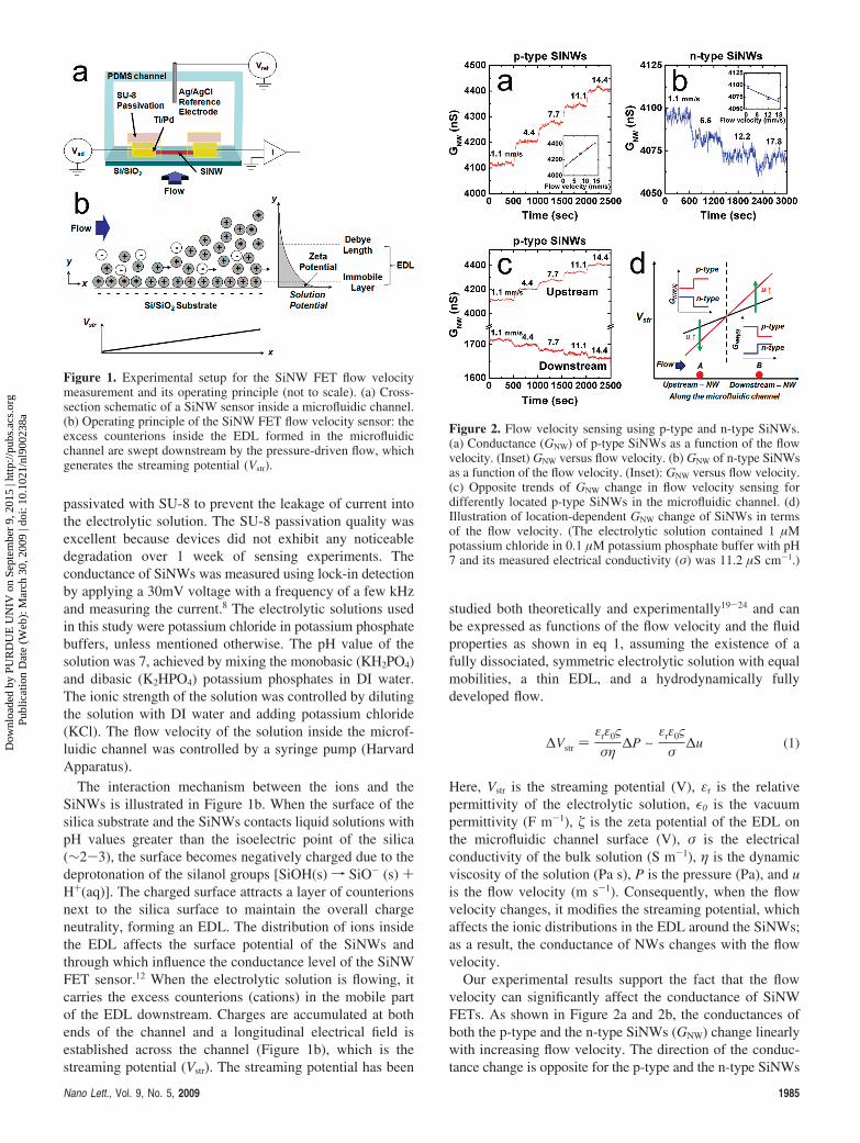
The interaction mechanism between the ions and theSiNWs is illustrated in Figure 1b. When the surface of thesilica substrate and the SiNWs contacts liquid solutions withpH values greater than the isoelectric point of the silica(∼2-3), the surface becomes negatively charged due to thedeprotonation of the silanol groups [SiOH(s) f SiO- (s) +H+(aq)]. The charged surface attracts a layer of counterionsnext to the silica surface to maintain the overall chargeneutrality, forming an EDL. The distribution of ions insidethe EDL affects the surface potential of the SiNWs andthrough which influence the conductance level of the SiNWFET sensor.12 When the electrolytic solution is flowing, itcarries the excess counterions (cations) in the mobile partof the EDL downstream. Charges are accumulated at bothends of the channel and a longitudinal electrical field isestablished across the channel (Figure 1b), which is thestreaming potential (Vstr). The streaming potential has been
studied both theoretically and experimentally19-24 and canbe expressed as functions of the flow velocity and the fluidproperties as shown in eq 1, assuming the existence of afully dissociated, symmetric electrolytic solution with equalmobilities, a thin EDL, and a hydrodynamically fullydeveloped flow.
Here, Vstr is the streaming potential (V), εr is the relativepermittivity of the electrolytic solution, ε0 is the vacuumpermittivity (F m-1), � is the zeta potential of the EDL onthe microfluidic channel surface (V), σ is the electricalconductivity of the bulk solution (S m-1), η is the dynamicviscosity of the solution (Pa s), P is the pressure (Pa), and uis the flow velocity (m s-1). Consequently, when the flowvelocity changes, it modifies the streaming potential, whichaffects the ionic distributions in the EDL around the SiNWs;as a result, the conductance of NWs changes with the flowvelocity.
Our experimental results support the fact that the flowvelocity can significantly affect the conductance of SiNWFETs. As shown in Figure 2a and 2b, the conductances ofboth the p-type and the n-type SiNWs (GNW) change linearlywith increasing flow velocity. The direction of the conduc-tance change is opposite for the p-type and the n-type SiNWs
Figure 1. Experimental setup for the SiNW FET flow velocitymeasurement and its operating principle (not to scale). (a) Cross-section schematic of a SiNW sensor inside a microfluidic channel.(b) Operating principle of the SiNW FET flow velocity sensor: theexcess counterions inside the EDL formed in the microfluidicchannel are swept downstream by the pressure-driven flow, whichgenerates the streaming potential (Vstr).
Figure 2. Flow velocity sensing using p-type and n-type SiNWs.(a) Conductance (GNW) of p-type SiNWs as a function of the flowvelocity. (Inset) GNW versus flow velocity. (b) GNW of n-type SiNWsas a function of the flow velocity. (Inset): GNW versus flow velocity.(c) Opposite trends of GNW change in flow velocity sensing fordifferently located p-type SiNWs in the microfluidic channel. (d)Illustration of location-dependent GNW change of SiNWs in termsof the flow velocity. (The electrolytic solution contained 1 µMpotassium chloride in 0.1 µM potassium phosphate buffer with pH7 and its measured electrical conductivity (σ) was 11.2 µS cm-1.)
∆Vstr )εrε0ςση
∆P ∼εrε0ς
σ∆u (1)
Nano Lett., Vol. 9, No. 5, 2009 1985
Dow
nloa
ded
by P
UR
DU
E U
NIV
on
Sept
embe
r 9,
201
5 | h
ttp://
pubs
.acs
.org
P
ublic
atio
n D
ate
(Web
): M
arch
30,
200
9 | d
oi: 1
0.10
21/n
l900
238a

because the same gate potential change has the oppositedepletion/accumulation effects on the p- and n-type SiNWs,respectively. The minimum velocity change which can bedetected by the p-type SiNW is in the range of 0.55-1.1mm s-1, which is more than one order of magnitude betterthan the reported flow velocity sensitivity of 20.83 mm s-1
using individual carbon nanotube FET sensors.25 To the bestof our knowledge, this is the first experimental demonstrationthat SiNW FET sensors can measure the flow velocity changethrough the streaming potential mechanism in an electrolyticsolution.
We further estimated the equivalent gate potential changeper unit flow velocity (∆VG,NW/∆u) for both the p-type andthe n-type SiNWs to compare the gate voltage change causedby the streaming potential. Specifically, the equivalent gatepotential change per unit flow velocity (∆VG,NW/∆u) wasestimated using eq 2, by dividing the averaged SiNWconductance change per flow velocity change (∆GNW/∆u)by the transconductance of SiNWs measured in the samesolution (∆GNW/∆VG,NW). The results are listed in Table 1.
The equivalent gate potential changes per unit flow velocityfor the p-type and the n-type SiNWs were very similar, at3.9 mV s mm-1 and 3.6 mV s mm-1, respectively. It shouldbe noted that the measured p- and n-type SiNWs were locatedat almost identical positions inside the microfluidic channeland with respect to the reference electrode. Therefore, theobserved near-equality of the local surface potential changeper unit flow velocity strongly suggests that SiNWs areresponding to the streaming potential change caused bythe fluidic motion of an electrolytic solution.
Furthermore, even SiNWs of the same doping type canexhibit opposite conductance changes in response to increas-ing flow velocity when the SiNWs are located upstream anddownstream of the reference electrode, respectively (Figure2c). Because the electrical potential of solution is fixed atthe center of the channel by the reference electrode (Figure2d), the solution potential at the downstream and upstreamlocations increases and decreases with increasing the flowvelocity, respectively. Consequently, even the same type ofSiNWs, depending upon their locations, can detect theopposite potential change and respond oppositely to the sameflow velocity change. This observation implies that the ionictransport will have different effects on FET sensors atdifferent locations inside the microfluidic channel. This isof concern in biosensing because if the local electric potentialchange caused by the ionic transport is greater than thatgenerated by the specific analyte-receptor binding event, it
may produce false signals, such as an opposite conductancechange.
The sensitivity of the flow velocity measurement for thep-type SiNW was further characterized as a function of theionic strength of the electrolytic solution. The ionic strengthof the potassium chloride solution (pH 7) was varied over abroad range, including strengths of 1, 10, 100, and 1000 µM.As shown in Figure 3a, the conductance of the p-type SiNW(GNW) increases monotonically with increasing flow velocityfor all the cases. However, the average amount of NWconductance change per unit flow velocity (∆GNW/∆u)decreases significantly as the ionic strength increases asshown in Figure 3b. The ionic strength affects the sensitivityof the flow velocity measurement by affecting both thesolution conductivity (σ) and the zeta potential (�) (eq 1).Specifically, the conductivity (σ) of the solution is linearlyproportional to its ionic strength,26,27 and the zeta potential
Table 1. Estimation of the Equivalent Gate PotentialChange Per Unit Flow Velocity Change
unit p-type SiNWs n-type SiNWs
∆GNW/∆VG,NW (nS mV-1) 5.60 0.45∆GNW/∆u (nS s mm-1) 21.8 1.6∆VG,NW/∆u (mV s mm-1) 3.9 3.6
∆VG,NW
∆u)
∆GNW/∆u
∆GNW/∆VG,NW)
∆Vstr
∆u∼
εrε0ςσ
(2) Figure 3. Effects of the ionic strength on the sensitivity of SiNWflow velocity sensing. (a) Flow velocity sensing of p-type SiNWsin potassium chloride solutions with ionic strengths of 1, 10, 100,and 1000 µM. (b) The SiNW conductance change per unit flowvelocity (∆GNW/∆u) with respect to the ionic strength (C). The solidline is a fitted curve, ∆GNW/∆u ) (-162.5 + 391.8 × log (C +10.9))/(C + 10.9), where C is in µM. (c) The SiNW conductance(GNW) versus the ionic strength (C) at different flow velocities. Allcurves show logarithmic fittings: GNW)5887.0-1265.0 × log(C+ 25.3) for u ) 1.1 mm s-1, GNW ) 5869.0-1258.0 × log(C +21.3) for u ) 4.4 mm s-1, GNW ) 5901.0-1268.0 × log(C + 19.1)for u ) 7.7 mm s-1, GNW ) 5920.0-1271.0 × log(C + 17.2) foru ) 11.1 mm s-1, and GNW ) 5944.0-1279.0 × log(C + 15.5)for u ) 14.4 mm s-1, where C is in µM.
1986 Nano Lett., Vol. 9, No. 5, 2009
Dow
nloa
ded
by P
UR
DU
E U
NIV
on
Sept
embe
r 9,
201
5 | h
ttp://
pubs
.acs
.org
P
ublic
atio
n D
ate
(Web
): M
arch
30,
200
9 | d
oi: 1
0.10
21/n
l900
238a

(�) has a logarithmic dependence on the ionic strength(� ∼ a0 + a1log C, where a0 and a1 are constants) for asymmetric electrolyte of C < 100 mM at pH >6.19 The changeof the streaming potential per unit flow velocity (∆Vstr/∆u),according to eq 1, is proportional to �/σ, and varies with theionic strength as (a0 + a1log C)/C. Furthermore, the SiNWswere selected to operate in the linear transconductanceregime. Thus, the conductance change of the SiNWs (∆GNW)is linearly proportional to the change of the streamingpotential (∆Vstr). Therefore, the conductance change ofSiNWs per unit flow velocity (∆GNW/∆u) varies with theionic strength as (a0 + a1log C)/C. Our experiments supportthis relation as shown in Figure 3b where the solid line is afitted curve of ∆GNW/∆u ) [-162.5 + 391.8 × log(C +10.9)]/(C + 10.9) and 10.9 is a concentration correction termto account for the surface conductivity of the microfluidicchannel.
Moreover, it can be seen from Figure 3c that theconductance levels of SiNWs (GNW) even at the same flowvelocity are different for solutions with different ionicstrengths and that GNW decreases logarithmically withincreasing ionic strength when the flow velocity and pH valueare fixed. For example, GNW can be related to the ionicstrength through the logarithmic fitting of GNW ) 5887.0 -1265.0 × log(C + 25.3) for u ) 1.1 mm s-1, where 25.3 is,again, a correction to account for the surface conductivity.The similar dependence of the baseline conductance of NWFETs on the ionic strength of the solution was also observedfor SnO2 nanobelt FET sensors in an aqueous solution.28 Thereason for this dependence is that the ionic strength affectsthe thickness of the EDL and the distribution of ions insideit. This changes the surface potential, through which theconductance of SiNWs is modified. The observation of theionic strength-dependent conductance of SiNWs implies thatSiNW FET sensors can potentially be utilized to measurethe ionic strength of an electrolytic solution. As for NWbiosensing, this observation indicates that the concentrationof the analyte should be much smaller than the concentrationof the buffer solution to prevent the conductance change ofNWs induced by the change in the ionic strength of the buffersolution with/without the analyte.
The sensitivity of the flow velocity measurement alsodepends on the compositions of the electrolytic solutionssince different solutions have different relative permittivityεr, zeta potential �, and electrical conductivity σ (eq 1). Forthe same n-type SiNW, the averaged conductance changein ethanol29 was 3.8 times higher than that in a 1 µMpotassium chloride solution for the same flow velocitychange, as shown in Figure 4a and 4b. This difference isconsistent with the streaming potential difference estimatedfrom their different properties according to eq 1 as shownin Table 2, where the estimated streaming potential change(∆Vstr) in ethanol is 3.2 times higher than that in 1 µMpotassium chloride, given the same flow velocity change.Hence, the larger conductance change of NWs (∆GNW) inethanol comes from the larger streaming potential changegenerated in ethanol. Again, it suggests that SiNWs measurethe flow velocity change by responding to changes in the
streaming potential. Furthermore, the observed enhancedsensitivity for measuring the flow velocity of ethanolindicates the versatility of the SiNW flow sensor and itspotential to distinguish different solutions.
In summary, we have demonstrated the first flow velocitysensing of an electrolytic solution in a microfluidic channelusing both the p-type and the n-type SiNW FET sensors.The conductance level of SiNWs reveals a clear andreproducible dependence on the flow velocity. The magnitudeof conductance change of the SiNWs (∆GNW) depends onthe ionic strength and the composition of the electrolyticsolution, and the direction of ∆GNW depends on the dopingtype of the SiNWs and the location of the SiNWs in themicrofluidic channel. Our quantitative analysis suggests thatflow velocity sensing is a consequence of the streamingpotential generated by the movement of counterions insidethe EDL. The streaming potential, which varies with the flowvelocity, the ionic strength and the composition of theelectrolytic solution, acts in the same way as charged analytesin affecting the conductance of SiNWs. This study demon-strates that in addition to the analyte binding events, theproperties and the velocity of the electrolytic solution cansignificantly change the conductance of NW FET sensorsand it is important to consider these factors in analyzing andoptimizing the sensing. Moreover, our study opens up a newtype of sensing application for NW sensors in probing thestreaming potentials, the flow velocity, the ionic strength,and more.
Acknowledgment. D.R.K. acknowledges support from theLink Foundation Energy Fellowship. X.L.Z. sincerely thanksthe Center of Integrated System at Stanford University andthe DARPA/YFA program for support of this work.
Figure 4. Effects of the ionic compositions on the sensitivity ofSiNW flow velocity sensing. The conductance of SiNW (GNW) asa function of the flow velocity in (a) a 1 µM potassium chloridesolution and (b) an ethanol solution.
Table 2. Comparison of the Streaming PotentialGenerated by the 1 µM Potassium Chloride Solution andEthanola
unit 1 µM potassium chloride ethanol34
εr 80.0 24.0� (mV) -100.0 -73.0σ (µS cm-1) 8.50 0.58∆Vstr ∼ ε�/σ 1.0 3.2
a The relative permittivity and the zeta potential for the 1 µM potassiumchloride solution were assumed to be the same as the DI water because thesolution was very dilute, and the electrical conductivity for both solutionswas measured.
Nano Lett., Vol. 9, No. 5, 2009 1987
Dow
nloa
ded
by P
UR
DU
E U
NIV
on
Sept
embe
r 9,
201
5 | h
ttp://
pubs
.acs
.org
P
ublic
atio
n D
ate
(Web
): M
arch
30,
200
9 | d
oi: 1
0.10
21/n
l900
238a
References(1) Schoch, R. B.; Han, J. Y.; Renaud, P. ReV. Mod. Phys. 2008, 80 (3),
839–883.(2) Cui, Y.; Wei, Q. Q.; Park, H. K.; Lieber, C. M. Science 2001, 293
(5533), 1289–1292.(3) Hahm, J.; Lieber, C. M. Nano Lett. 2004, 4 (1), 51–54.(4) Patolsky, F.; Zheng, G. F.; Hayden, O.; Lakadamyali, M.; Zhuang,
X. W.; Lieber, C. M. Proc. Natl. Acad. Sci. U.S.A. 2004, 101 (39),14017–14022.
(5) Patolsky, F.; Zheng, G.; Lieber, C. M. Nanomedicine 2006, 1 (1),51–65.
(6) Patolsky, F.; Lieber, C. M. Mater. Today 2005, 8 (5), 20–28.(7) Stern, E.; Klemic, J. F.; Routenberg, D. A.; Wyrembak, P. N.; Turner-
Evans, D. B.; Hamilton, A. D.; LaVan, D. A.; Fahmy, T. M.; Reed,M. A. Nature 2007, 445 (7127), 519–522.
(8) Patolsky, F.; Zheng, G. F.; Lieber, C. M. Nat. Protoc. 2006, 1 (4),1711–1724.
(9) Nair, P. R.; Alam, M. A. Appl. Phys. Lett. 2006, 88 (23), 233120.(10) Squires, T. M.; Messinger, R. J.; Manalis, S. R. Nat. Biotechnol. 2008,
26 (4), 417–426.(11) Kim, D. R.; Zheng, X. L. Nano Lett. 2008, 8 (10), 3233–3237.(12) Shinwari, M. W.; Deen, M. J.; Landheer, D. Microelecton. Reliab.
2007, 47 (12), 2025–2057.(13) Minot, E. D.; Janssens, A. M.; Heller, I.; Heering, H. A.; Dekker, C.;
Lemay, S. G. Appl. Phys. Lett. 2007, 91 (9), 093507.(14) Polk, B. J.; Stelzenmuller, A.; Mijares, G.; MacCrehan, W.; Gaitan,
M. Sens. Actuators, B 2006, 114 (1), 239–247.(15) Wagner, R. S.; Ellis, W. C. Appl. Phys. Lett. 1964, 4 (5), 89–90.(16) Cui, Y.; Lauhon, L. J.; Gudiksen, M. S.; Wang, J. F.; Lieber, C. M.
Appl. Phys. Lett. 2001, 78 (15), 2214–2216.(17) Both the p-type and the n-type SiNWs were synthesized by chemical
vapor deposition with 20 nm gold catalysts in a quartz tube furnace.For the p-type SiNWs, the feeding ratio of Si:B was 4000:1, and thegrowth condition was 440°C, 40 Torr, 10 sccm of Ar, 2.5 sccm ofSiH4, and 3 sccm of 10000:1 H2 diluted B2H6. For the n-type SiNWs,the feeding ratio of Si:P was 2000:1, 450°C, 40 Torr, 10 sccm of Ar,2.5 sccm of SiH4, and 1.25 sccm of 1000:1 H2 diluted PH3. The growthtime was 15 min.
(18) Devices were fabricated on degenerately doped silicon wafers with500 nm thermally grown oxides. SiNWs suspended in an ethanolsolution were deposited onto the silicon substrate, and the source anddrain electrodes were defined by photolithography, metallization ofTi/Pd (2 nm/50 nm) by an electron beam evaporator, and lift-off. Thedevices were further passivated by 2 µm of SU-8 (Microchem Corp.)with a second photolithography step.
(19) Kirby, B. J.; Hasselbrink, E. F. Electrophoresis 2004, 25 (2), 187–202.
(20) van der Heyden, F. H. J.; Stein, D.; Dekker, C. Phys. ReV. Lett. 2005,95 (11), 116104.
(21) Mansouri, A.; Scheuerman, C.; Bhattacharjee, S.; Kwok, D. Y.;Kostiuk, L. W. J. Colloid Interface Sci. 2005, 292 (2), 567–580.
(22) Vanwagenen, R. A.; Andrade, J. D. J. Colloid Interface Sci. 1980, 76(2), 305–314.
(23) Chun, M. S.; Lee, T. S.; Choi, N. W. J. Micromech. Microeng. 2005,15 (4), 710–719.
(24) Burgreen, D.; Nakache, F. R. J. Phys. Chem. 1964, 68 (5), 1084–1091.
(25) Bourlon, B.; Wong, J.; Miko, C.; Forro, L.; Bockrath, M. Nat.Nanotechnol. 2007, 2 (2), 104–107.
(26) Probstein, R. F. Physicochemical Hydrodynamics, 2nd ed.; WileyInterscience: New York, 2003.
(27) σ ) ∑i ) 1N F2zi
2µiCi (S m-1), where the summation is over all the ionicspecies, F is Faraday’s constant (c mol-1), zi is the valency of eachionic species, µi is the mobility of the ionic species (mol s kg-1), andCi is the ionic concentration (mol m-3).
(28) Cheng, Y.; Yun, C. S.; Strouse, G. F.; Zheng, J. P.; Yang, R. S.; Wang,Z. L. Nano Lett. 2008, 8 (12), 4179–4184.
(29) Ethanol (CH3CH2OH) is an amphiprotic solvent that can accept anddonate protons through autoprotolysis reaction [2CH3CH2OH(aq) TCH3CH2O-(aq) + CH3CH2OH2
+(aq)] (see refs 30 and 31). Amphipro-tic solvents can also accept or donate protons if the system containsother proton donors/acceptors, such as the silica surface (Si-OH) orimpurities like water (see refs 32 and 33). The existence of ions inethanol is supported by the fact that the zeta potential of silica surfacein ethanol was measured to be -72.6 mV (see ref 34). Moreover,streaming potential has been measured in ethanol and the reportedstreaming potential in ethanol was 2.4 times higher than that in water(see ref 35).
(30) Letcher, T. M., DeVelopments and Applications in Solubility; RoyalSociety of Chemistry: London, 2007.
(31) Kim, D.; Posner, J. D.; Santiago, J. G. Sens. Actuators, A 2008, 141(1), 201–212.
(32) Sharp, K. G. J. Sol-Gel Sci. Technol. 1994, 2, 35–41.(33) Kilic, E.; Aslan, N. Microchim. Acta 2005, 151, 89–92.(34) Valko, I. E.; Siren, H.; Riekkola, M. L. J. Microcolumn Sep. 1999,
11 (3), 199–208.(35) Caldwell, K. D.; Myers, M. N. Anal. Chem. 1986, 58 (7), 1583–1585.
NL900238A
1988 Nano Lett., Vol. 9, No. 5, 2009
Dow
nloa
ded
by P
UR
DU
E U
NIV
on
Sept
embe
r 9,
201
5 | h
ttp://
pubs
.acs
.org
P
ublic
atio
n D
ate
(Web
): M
arch
30,
200
9 | d
oi: 1
0.10
21/n
l900
238a