Preparation and Characterization of TiO2 Nanotube Arrays ...
8
Electrochimica Acta 136 (2014) 404–411 Contents lists available at ScienceDirect Electrochimica Acta j our na l ho me pa g e: www.elsevier.com/locate/electacta Preparation and Characterization of TiO 2 Nanotube Arrays in Ionic Liquid for Water Splitting R.G. Freitas, M.A. Santanna, E.C. Pereira ∗ NANOFAEL – LIEC – Departamento de Química. Universidade Federal de São Carlos – C.P.: 676 – CEP: 13565-905, São Carlos, SP, Brazil a r t i c l e i n f o Article history: Received 27 March 2014 Accepted 18 May 2014 Available online 27 May 2014 Keywords: TiO2 nanotubes water splitting electron lifetime photocurrent transients a b s t r a c t In the present work, it is described the fabrication and characterization of TiO 2 nantotubes prepared potentiostatically using 1.0 or 5.0 vol.% ionic liquid electrolyte medium at 10 or 20 ◦ C. These experimental conditions led to TiO 2 nanotubes with 63-77 nm pore diameter, crystallite sizes between 27-33 nm, and band-gap values in the 3.1-3.2 eV range. Although the morphology and band-gap values were similar, the water splitting reaction showed differences in terms of photocurrent, up to 300%. Besides, we report also important changes in those parameters related with electronic defects, such as carrier density (N D ), width of depletion layer (w) and Debye length ( D ). Then, the enhancement on photoelectrochemical properties could be related to a decrease in the rate of surface recombination processes. Finally, these proposition are in agreement with the open-circuit voltage-decay, where was observed a higher electron lifetime for TiO 2 NT obtained at higher vol.% of ionic liquid. © 2014 Elsevier Ltd. All rights reserved. 1. Introduction Efficient splitting of water into H 2 /O 2 , photocatalytically acti- vated, is probably the most desired pathway to convert abundant solar energy into “hydrogen”, the proposed clean energy carrier of the future. The total amount of solar energy impinging on the earth‘s surface in one year is about 3x10 24 J, or approximately 10 4 times the worldwide yearly consumption of energy [1]. The search for efficient conversion of solar energy into other useful forms is, in view of the increasing anxiety over the exhaustion of fossil energy resources and attendant global warming, one of the most important challenges for future. However, there are three major important tasks for the solar production of hydrogen: (1) Stability. Metal oxides are the most photochemically stable semiconductors in aqueous solution, but their band-gaps are either too large (≈3.0 eV) to absorb a significant fraction of incident solar energy, or their semiconductor charac- teristics (e.g. charge transport) are poor [2]. (2) Band-gap values. Considering the water splitting energy of 1.23 eV and overpotential losses, the semiconductor(s) should have a band-gap greater than 1.7 eV. However, semiconductors with relative low band-gaps have been found to lack stability during water splitting [2]. (3) Energy level edge position. Even though a semiconductor may generate suf- ficient energy to drive an electrochemical reaction, the band edge ∗ Corresponding author. Tel.: +55 16 3351 8214; fax: +55 16 3351 8214. E-mail addresses: [email protected], [email protected] (E.C. Pereira). position may prevent it from react leading to water splitting [2]. For spontaneous water splitting, water oxidation and reduction potential must lie between the valence and conduction band edges. Among inorganic oxides, TiO 2 is an important candidate for efficiently water splitting reaction. Several papers in the litera- ture [3,4] have demonstrated that besides the microstructure, the morphology is important to optimize the oxide properties. Then, TiO 2 nanotubes (TiO 2 NT) seem to be a promise material as pho- toanode to water splitting application, once these nanostructures provide unique electronic properties, such as high electron mobil- ity [5], appropriated band edge positions [6], quantum confinement effects [7], high specific surface area [8], high mechanical strength [9] and photocorrosion resistance [10]. In this scenario, TiO 2 NTs seem to be a versatile compound and one of the most investigated nanostructure in materials science. Among the factors that affect the TiO 2 NT properties, elec- trochemically obtained, the non-aqueous electrolyte can be regarded as a very important variable. In this context, ionic liquid (IL) have many applications, such as powerful solvents and electrically conducting fluids (electrolytes). Specifically dur- ing titanium anodization, the use of a fluor salt which is liquid at ambient temperature, such as 1-butyl-3-methyl-imidazolium- tetrafluoroborate (BMIM-BF 4 ), is important as fluoride precursors source which determine the quality, morphology and density of the nanotubes. The use of ionic liquid as electrolyte during the TiO 2 NTs obtainment by electrochemical means is quite recent, and just few papers have reported it. Schmuki et al. [11] observed the formation of well-ordered self-organized TiO 2 nanotube layers in BMIN-BF 4 http://dx.doi.org/10.1016/j.electacta.2014.05.097 0013-4686/© 2014 Elsevier Ltd. All rights reserved.
Transcript of Preparation and Characterization of TiO2 Nanotube Arrays ...

PL
RN
a
ARAA
KTwep
1
vsoetfvrc
pptftCl1blfi
h0
Electrochimica Acta 136 (2014) 404–411
Contents lists available at ScienceDirect
Electrochimica Acta
j our na l ho me pa g e: www.elsev ier .com/ locate /e lec tac ta
reparation and Characterization of TiO2 Nanotube Arrays in Ioniciquid for Water Splitting
.G. Freitas, M.A. Santanna, E.C. Pereira ∗
ANOFAEL – LIEC – Departamento de Química. Universidade Federal de São Carlos – C.P.: 676 – CEP: 13565-905, São Carlos, SP, Brazil
r t i c l e i n f o
rticle history:eceived 27 March 2014ccepted 18 May 2014vailable online 27 May 2014
eywords:
a b s t r a c t
In the present work, it is described the fabrication and characterization of TiO2 nantotubes preparedpotentiostatically using 1.0 or 5.0 vol.% ionic liquid electrolyte medium at 10 or 20 ◦C. These experimentalconditions led to TiO2 nanotubes with 63-77 nm pore diameter, crystallite sizes between 27-33 nm, andband-gap values in the 3.1-3.2 eV range. Although the morphology and band-gap values were similar,the water splitting reaction showed differences in terms of photocurrent, up to 300%. Besides, we report
iO2 nanotubesater splitting
lectron lifetimehotocurrent transients
also important changes in those parameters related with electronic defects, such as carrier density (ND),width of depletion layer (w) and Debye length (�D). Then, the enhancement on photoelectrochemicalproperties could be related to a decrease in the rate of surface recombination processes. Finally, theseproposition are in agreement with the open-circuit voltage-decay, where was observed a higher electronlifetime for TiO2NT obtained at higher vol.% of ionic liquid.
. Introduction
Efficient splitting of water into H2/O2, photocatalytically acti-ated, is probably the most desired pathway to convert abundantolar energy into “hydrogen”, the proposed clean energy carrierf the future. The total amount of solar energy impinging on thearth‘s surface in one year is about 3x1024 J, or approximately 104
imes the worldwide yearly consumption of energy [1]. The searchor efficient conversion of solar energy into other useful forms is, iniew of the increasing anxiety over the exhaustion of fossil energyesources and attendant global warming, one of the most importanthallenges for future.
However, there are three major important tasks for the solarroduction of hydrogen: (1) Stability. Metal oxides are the mosthotochemically stable semiconductors in aqueous solution, butheir band-gaps are either too large (≈3.0 eV) to absorb a significantraction of incident solar energy, or their semiconductor charac-eristics (e.g. charge transport) are poor [2]. (2) Band-gap values.onsidering the water splitting energy of 1.23 eV and overpotential
osses, the semiconductor(s) should have a band-gap greater than.7 eV. However, semiconductors with relative low band-gaps have
een found to lack stability during water splitting [2]. (3) Energyevel edge position. Even though a semiconductor may generate suf-cient energy to drive an electrochemical reaction, the band edge
∗ Corresponding author. Tel.: +55 16 3351 8214; fax: +55 16 3351 8214.E-mail addresses: [email protected], [email protected] (E.C. Pereira).
ttp://dx.doi.org/10.1016/j.electacta.2014.05.097013-4686/© 2014 Elsevier Ltd. All rights reserved.
© 2014 Elsevier Ltd. All rights reserved.
position may prevent it from react leading to water splitting [2].For spontaneous water splitting, water oxidation and reductionpotential must lie between the valence and conduction band edges.
Among inorganic oxides, TiO2 is an important candidate forefficiently water splitting reaction. Several papers in the litera-ture [3,4] have demonstrated that besides the microstructure, themorphology is important to optimize the oxide properties. Then,TiO2 nanotubes (TiO2NT) seem to be a promise material as pho-toanode to water splitting application, once these nanostructuresprovide unique electronic properties, such as high electron mobil-ity [5], appropriated band edge positions [6], quantum confinementeffects [7], high specific surface area [8], high mechanical strength[9] and photocorrosion resistance [10]. In this scenario, TiO2NTsseem to be a versatile compound and one of the most investigatednanostructure in materials science.
Among the factors that affect the TiO2NT properties, elec-trochemically obtained, the non-aqueous electrolyte can beregarded as a very important variable. In this context, ionicliquid (IL) have many applications, such as powerful solventsand electrically conducting fluids (electrolytes). Specifically dur-ing titanium anodization, the use of a fluor salt which is liquidat ambient temperature, such as 1-butyl-3-methyl-imidazolium-tetrafluoroborate (BMIM-BF4), is important as fluoride precursorssource which determine the quality, morphology and density of the
nanotubes. The use of ionic liquid as electrolyte during the TiO2NTsobtainment by electrochemical means is quite recent, and just fewpapers have reported it. Schmuki et al. [11] observed the formationof well-ordered self-organized TiO2 nanotube layers in BMIN-BF4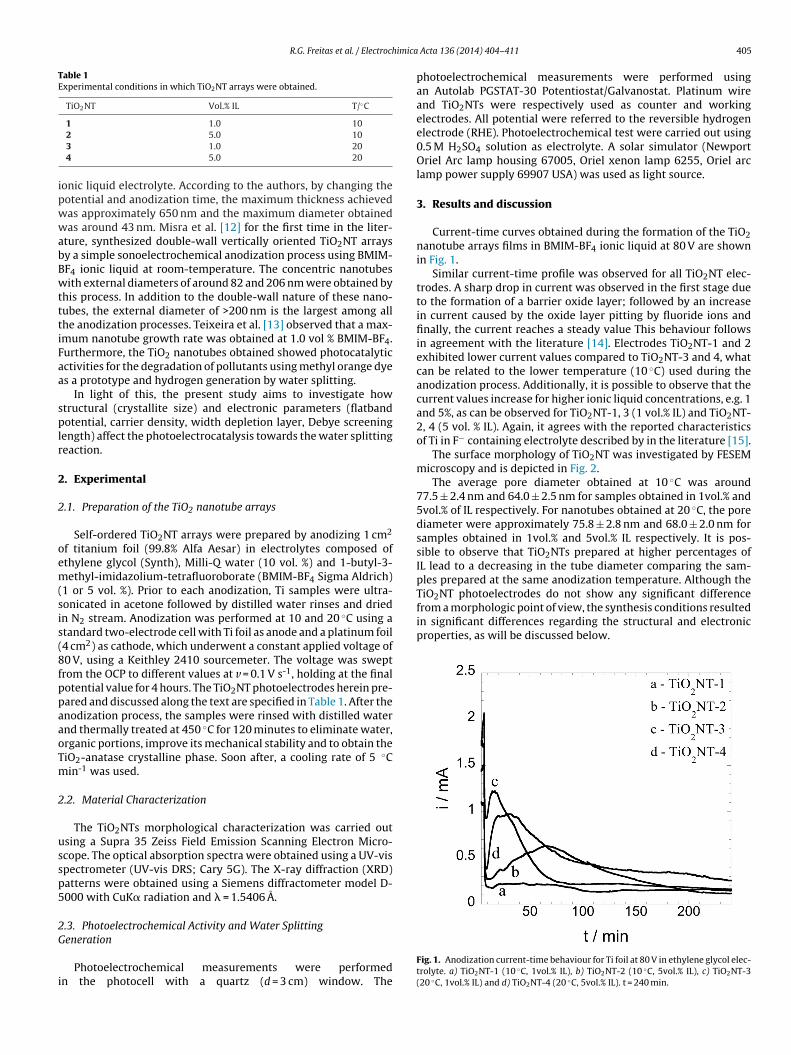
R.G. Freitas et al. / Electrochimica
Table 1Experimental conditions in which TiO2NT arrays were obtained.
TiO2NT Vol.% IL T/◦C
1 1.0 10
ipwwabBwtttiFaa
splr
2
2
oem(sis(8fppaaoTm
2
ussp5
2G
i
TiO2NT photoelectrodes do not show any significant differencefrom a morphologic point of view, the synthesis conditions resultedin significant differences regarding the structural and electronicproperties, as will be discussed below.
2 5.0 103 1.0 204 5.0 20
onic liquid electrolyte. According to the authors, by changing theotential and anodization time, the maximum thickness achievedas approximately 650 nm and the maximum diameter obtainedas around 43 nm. Misra et al. [12] for the first time in the liter-
ture, synthesized double-wall vertically oriented TiO2NT arraysy a simple sonoelectrochemical anodization process using BMIM-F4 ionic liquid at room-temperature. The concentric nanotubesith external diameters of around 82 and 206 nm were obtained by
his process. In addition to the double-wall nature of these nano-ubes, the external diameter of >200 nm is the largest among allhe anodization processes. Teixeira et al. [13] observed that a max-mum nanotube growth rate was obtained at 1.0 vol % BMIM-BF4.urthermore, the TiO2 nanotubes obtained showed photocatalyticctivities for the degradation of pollutants using methyl orange dyes a prototype and hydrogen generation by water splitting.
In light of this, the present study aims to investigate howtructural (crystallite size) and electronic parameters (flatbandotential, carrier density, width depletion layer, Debye screening
ength) affect the photoelectrocatalysis towards the water splittingeaction.
. Experimental
.1. Preparation of the TiO2 nanotube arrays
Self-ordered TiO2NT arrays were prepared by anodizing 1 cm2
f titanium foil (99.8% Alfa Aesar) in electrolytes composed ofthylene glycol (Synth), Milli-Q water (10 vol. %) and 1-butyl-3-ethyl-imidazolium-tetrafluoroborate (BMIM-BF4 Sigma Aldrich)
1 or 5 vol. %). Prior to each anodization, Ti samples were ultra-onicated in acetone followed by distilled water rinses and driedn N2 stream. Anodization was performed at 10 and 20 ◦C using atandard two-electrode cell with Ti foil as anode and a platinum foil4 cm2) as cathode, which underwent a constant applied voltage of0 V, using a Keithley 2410 sourcemeter. The voltage was sweptrom the OCP to different values at v = 0.1 V s-1, holding at the finalotential value for 4 hours. The TiO2NT photoelectrodes herein pre-ared and discussed along the text are specified in Table 1. After thenodization process, the samples were rinsed with distilled waternd thermally treated at 450 ◦C for 120 minutes to eliminate water,rganic portions, improve its mechanical stability and to obtain theiO2-anatase crystalline phase. Soon after, a cooling rate of 5 ◦Cin-1 was used.
.2. Material Characterization
The TiO2NTs morphological characterization was carried outsing a Supra 35 Zeiss Field Emission Scanning Electron Micro-cope. The optical absorption spectra were obtained using a UV-vispectrometer (UV-vis DRS; Cary 5G). The X-ray diffraction (XRD)atterns were obtained using a Siemens diffractometer model D-000 with CuK� radiation and � = 1.5406 A.
.3. Photoelectrochemical Activity and Water Splitting
enerationPhotoelectrochemical measurements were performedn the photocell with a quartz (d = 3 cm) window. The
Acta 136 (2014) 404–411 405
photoelectrochemical measurements were performed usingan Autolab PGSTAT-30 Potentiostat/Galvanostat. Platinum wireand TiO2NTs were respectively used as counter and workingelectrodes. All potential were referred to the reversible hydrogenelectrode (RHE). Photoelectrochemical test were carried out using0.5 M H2SO4 solution as electrolyte. A solar simulator (NewportOriel Arc lamp housing 67005, Oriel xenon lamp 6255, Oriel arclamp power supply 69907 USA) was used as light source.
3. Results and discussion
Current-time curves obtained during the formation of the TiO2nanotube arrays films in BMIM-BF4 ionic liquid at 80 V are shownin Fig. 1.
Similar current-time profile was observed for all TiO2NT elec-trodes. A sharp drop in current was observed in the first stage dueto the formation of a barrier oxide layer; followed by an increasein current caused by the oxide layer pitting by fluoride ions andfinally, the current reaches a steady value This behaviour followsin agreement with the literature [14]. Electrodes TiO2NT-1 and 2exhibited lower current values compared to TiO2NT-3 and 4, whatcan be related to the lower temperature (10 ◦C) used during theanodization process. Additionally, it is possible to observe that thecurrent values increase for higher ionic liquid concentrations, e.g. 1and 5%, as can be observed for TiO2NT-1, 3 (1 vol.% IL) and TiO2NT-2, 4 (5 vol. % IL). Again, it agrees with the reported characteristicsof Ti in F− containing electrolyte described by in the literature [15].
The surface morphology of TiO2NT was investigated by FESEMmicroscopy and is depicted in Fig. 2.
The average pore diameter obtained at 10 ◦C was around77.5 ± 2.4 nm and 64.0 ± 2.5 nm for samples obtained in 1vol.% and5vol.% of IL respectively. For nanotubes obtained at 20 ◦C, the porediameter were approximately 75.8 ± 2.8 nm and 68.0 ± 2.0 nm forsamples obtained in 1vol.% and 5vol.% IL respectively. It is pos-sible to observe that TiO2NTs prepared at higher percentages ofIL lead to a decreasing in the tube diameter comparing the sam-ples prepared at the same anodization temperature. Although the
Fig. 1. Anodization current-time behaviour for Ti foil at 80 V in ethylene glycol elec-trolyte. a) TiO2NT-1 (10 ◦C, 1vol.% IL), b) TiO2NT-2 (10 ◦C, 5vol.% IL), c) TiO2NT-3(20 ◦C, 1vol.% IL) and d) TiO2NT-4 (20 ◦C, 5vol.% IL). t = 240 min.

406 R.G. Freitas et al. / Electrochimica Acta 136 (2014) 404–411
F a) TiOa
ac(
Frb
ig. 2. FESEM images of TiO2NT arrays grown in different conditions. Tube diameter:nd d) TiO2NT-4, d∼68.0 ± 2.0 nm.
As can be observed by the X-ray diffraction patterns in Fig. 3,ll TiO2NT samples crystallized in the anatase phase, which isharacterized by peaks at 2� = 25.281 (101) and 2� = 48.049 (200)JCPDS – 21-1272). The TiO2NT self-ordered film was thin, as
ig. 3. XRD patterns of the TiO2NTs arrays annealed at 450 ◦C for 2 hours. A, R, Tiepresent anatase, rutile and titanium diffraction peaks respectively. a) TiO2NT-1,) TiO2NT-2, c) TiO2NT-3 and d) TiO2NT-4.
2NT-1, d∼77.5 ± 2.4 nm, b) TiO2NT-2, d∼64.0 ± 2.5 nm, c) TiO2NT-3, d∼75.8 ± 2.8 nm
metallic titanium peaks were also observed (JCPDS 44-1294) athigher intensities rather than anatase-TiO2 ones. Also, a smallamount of rutile-TiO2 crystalline phase was detected at 2� = 27.446(110) and 2� = 36.085 (101) (JCPDS – 21-1276).
The crystallite sizes (CS) were calculated using the Debye-Scherrer equation from the anatase (101) peak. The values obtainedwere 27.0, 28.0, 30.0 and 33.5 nm for TiO2NT-1, 2, 3 and 4 pho-toelectrode respectively, as shown in Table 2. Considering theexperimental error, the CS are the same for all the prepared sam-ples. These values are similar to those previously reported in theliterature [14,16] for TiO2NT electrodes.
The band-gap, Eg, was estimated using the Tauc-Wood equation[17]:
(˛h�)s = h� − Eg (1)
where � is the absorption coefficient, hv and Eg are photon energyand optical band-gap energy, respectively. The value used for s was0.5 once TiO2 is classified an indirect gap semiconductor. Eg valueswere thus determined by extrapolation of the linear portion of the
Table 2Structural and electronic parameters obtained from XRD and Mott-Schottky mea-surements for TiO2NT arrays.
TiO2NT C.S./nm EFB/V ND/cm-3 w/nm �D/nm
1 27.0 1.11 6.8x10¹⁸ 7.7 1.42 28.0 1.25 5.5x10¹⁸ 6.7 1.63 30.0 1.2 1.5x10¹⁹ 4.5 0.954 33.5 1.26 1.3x10¹⁹ 4.2 1.0
R.G. Freitas et al. / Electrochimica Acta 136 (2014) 404–411 407
Fig. 4. Plot of (�hv)0.5 vs. hv for the estimation of the TiO NT band-gap energy. a)T
(iftebpseioETi
rgtsTdT[ttct
opo
dcitrUTUt
Fig. 5. a) Photocurrent transients generated during photoirradiation under UV-Visible light, b) zoomed in photocurrent transients *circled-signed in a) and c)
2
iO2NT-1, b) TiO2NT-2, c) TiO2NT-3 and d) TiO2NT-4.
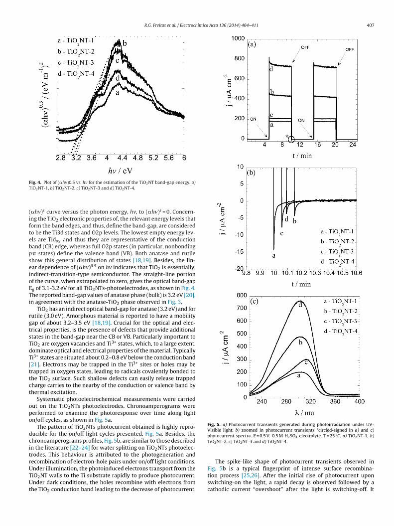
�hv)s curve versus the photon energy, hv, to (�hv)s = 0. Concern-ng the TiO2 electronic properties of, the relevant energy levels thatorm the band edges, and thus, define the band-gap, are consideredo be the Ti3d states and O2p levels. The lowest empty energy lev-ls are Tidxy and thus they are representative of the conductionand (CB) edge, whereas full O2p states (in particular, nonbonding� states) define the valence band (VB). Both anatase and rutilehow this general distribution of states [18,19]. Besides, the lin-ar dependence of (�hv)0.5 on hv indicates that TiO2 is essentially,ndirect-transition-type semiconductor. The straight-line portionf the curve, when extrapolated to zero, gives the optical band-gapg of 3.1-3.2 eV for all TiO2NTs-photoelectrodes, as shown in Fig. 4.he reported band-gap values of anatase phase (bulk) is 3.2 eV [20],n agreement with the anatase-TiO2 phase observed in Fig. 3.
TiO2 has an indirect optical band-gap for anatase (3.2 eV) and forutile (3.0 eV). Amorphous material is reported to have a mobilityap of about 3.2–3.5 eV [18,19]. Crucial for the optical and elec-rical properties, is the presence of defects that provide additionaltates in the band-gap near the CB or VB. Particularly important toiO2 are oxygen vacancies and Ti3+ states, which, to a large extent,ominate optical and electrical properties of the material. Typicallyi3+ states are situated about 0.2–0.8 eV below the conduction band21]. Electrons may be trapped in the Ti3+ sites or holes may berapped in oxygen states, leading to radicals covalently bonded tohe TiO2 surface. Such shallow defects can easily release trappedharge carries to the nearby of the conduction or valence band byhermal excitation.
Systematic photoelectrochemical measurements were carriedut on the TiO2NTs photoelectrodes. Chronoamperograms wereerformed to examine the photoresponse over time along lightn/off cycles, as shown in Fig. 5a.
The pattern of TiO2NTs photocurrent obtained is highly repro-ucible for the on/off light cycles presented, Fig. 5a. Besides, thehronoamperograms profiles, Fig. 5b, are similar to those describedn the literature [22–24] for water splitting on TiO2NTs photoelec-rodes. This behaviour is attributed to the photogeneration andecombination of electron-hole pairs under on/off light conditions.nder illumination, the photoinduced electrons transport from the
iO2NT walls to the Ti substrate rapidly to produce photocurrent.nder dark conditions, the holes recombine with electrons fromhe TiO2 conduction band leading to the decrease of photocurrent.
photocurrent spectra. E = 0.5 V. 0.5 M H2SO4 electrolyte. T = 25 ◦C. a) TiO2NT-1, b)TiO2NT-2, c) TiO2NT-3 and d) TiO2NT-4.
The spike-like shape of photocurrent transients observed inFig. 5b is a typical fingerprint of intense surface recombina-
tion process [25,26]. After the initial rise of photocurrent uponswitching-on the light, a rapid decay is observed followed by acathodic current “overshoot” after the light is switching-off. It
4 imica Acta 136 (2014) 404–411
sstarrro%rIsFc
tacstiao
tpat(vcawFpeiie2tm
dpvitgawFieadeudl
mdt
r
Fig. 6. Electron lifetime measurements determined form the open-circuit voltage-
08 R.G. Freitas et al. / Electroch
uggests that the photogenerated holes are being trapped in theurface states too deeply to induce efficient water oxidation andherefore, accumulating at the surface. This increases the prob-bility of conduction band electrons to be captured, inducingecombination rather than photocurrents. When the light is inter-upted, the holes accumulated in surface states still continue toecombine for some time, and so a cathodic current overshoot isbserved. As a result, TiO2NTs electrodes prepared at higher vol.
IL i.e. TiO2NT-2 and 4 photoelectrodes, exhibited lower surfaceecombination process compared to those obtained at lower vol. %L (TiO2NT-1 and 3 photoelectrodes). As consequence of the lowerurface recombination process exhibited by TiO2NT-4 (observed inig. 5b), such photoelectrodes also exhibited higher peak photo-urrent depicted by Fig. 5a and 5c, as described below.
It is possible to observe in Fig. 5a, that TiO2NTs-2 and 4 elec-rodes exhibited a higher photocurrent compared to TiO2NTs-1nd 3 photoelectrodes. One possible explanation is that higheroncentration of IL leads to an increasing in the photoelectrocataly-is. Also, the photocurrent increased 305% for TiO2NT-4, comparedo the TiO2NT-1 photoelectrode. An explanation for the increasen the peak photocurrent for higher vol. % IL TiO2NTs preparedt the same anodization temperature, can be explained in lightf Fig. 5b.
In order to estimate how the concentration of IL and the anodiza-ion temperature affect the photocurrent along the UV range, thehotocurrent spectra are shown in Fig. 5c. It is possible to observen increasing of 295% in the photocurrent for TiO2NT-4 comparedo TiO2NT-1 photoelectrodes. This value is in agreement with thati.e. 305%) obtained in Fig. 5a. Such increase in the photocurrentalues is related to the decrease in the surface recombination pro-ess, as discussed in Fig. 5b. All TiO2NTs show a peak wavelengthround 300 nm. These peak wavelength values are in agreementith the literature. Lin et al. [27] studied the strategy of doping
e3+ into TiO2NT to enhance its photocatalytic activity. The peakhotocurrent for TiO2NT-Fedoped observed was near 325 nm. Lint al. [28] also studied the water splitting under TiO2NT with plat-num nanoparticles. The authors also observed a maximum on thencidence photon current efficiency on the UV-region. Augustynskit al. [29] observed a maximum in the photocurrent efficiency at80 nm for nanocrystalline TiO2 films. Finally, Jin et al. [30] studiedhe photoelectrooxidation of methanol in TiO2NT, and observed a
aximum in the photocurrent density near 250 nm.Open-circuit voltage-decay (OCVD) measurements were con-
ucted to investigate the recombination kinetics of the TiO2NTshotoelectrodes. According to Kamat et al. [31], the open-circuitoltage of the photoelectrochemical cell represents the differencen Fermi level between TiO2NT and counter electrodes. In the dark,he electrode potential is dictated by the redox equilibrium. Band-ap excitation of TiO2 results in charge separation. As the holesre scavenged by H2O at the interface, the electrons accumulateithin the TiO2NTs. Electrons accumulation causes a shift in the
ermi level to more negative potentials, and it reflects in an increasen the VOC. The open-circuit voltage reaches a maximum as thelectron accumulation competes with the charge recombinationnd this attains a steady state. Upon stopping the illumination, VOCecays as the electrons accumulated within the TiO2NT are scav-nged by acceptor species in the electrolyte (e.g. H+) as well asndergo recombination with trapped holes. Thus monitoring theecay of the voltage provides an insight into the pathways by which
oss of accumulated electrons occurs within TiO2NT.Following the technique as reported by Bisquert et al. [32], OCVD
easurements were performed by monitoring the VOC transients
uring relaxation from an illuminated quasi-equilibrium state tohe dark equilibrium, see Fig. 6-inset.When the illumination on the TiO2NT photoelectrodes is inter-upted, the excess electrons are removed due to recombination,
decay in dark-inset. Inset: the curves of open-circuit photovoltage-decay of theTiO2NT arrays. 0.5 M H2SO4 electrolyte. T = 25 ◦C. a) TiO2NT-1, b) TiO2NT-2, c)TiO2NT-3 and d) TiO2NT-4.
with a photovoltage decay rate directly related to the electron life-time, by the following expression:
� = kBT
e
(∂VOC
∂t
)−1
(2)
where the thermal energy is given by kBT, e is the positive elemen-tary charge, and ∂VOC/∂t is the derivative of the open circuit voltagetransient. Fig. 6 is the plot of the response time obtained by apply-ing Eq. 2 to the data in Fig. 6-inset. In general, the recombinationreaction in photoelectrodes is a nonlinear property that shows asecond order behaviour with respect to the electron concentration.The shape of the VOC curve shows a dependence on the quasi-fermilevel, confirming a trap-assisted conduction mechanism [32]. Thismeans that the effective recombination contains contribution notonly from the free carriers, but also from the trapping, detrap-ping and charge-transfer mechanism. Moreover, the minor delayin the electron lifetime through trapping and detrapping eventsis also expected considering the various TiO2 crystallite phasesencountered along the tubular structure of the TiO2NTs. The shorterlifetimes observed at low VOC in Fig. 6 are related to the charge-transfer delay.
It is possible to observe also that in comparison to reportedOCVD measurements, TiO2NT photoelectrodes prepared at highervol.% IL (TiO2NT-2, 4 photoelectrode) exhibited longer lifetimesprepared at the same temperature anodization. Therefore, fewerrecombination centers can be observed for those samples preparedusing a high vol.% IL. It is important to stress out that these datacorroborates different aspects:i) the higher photocurrent observedin Fig. 5a, ii) the lower cathodic current values (spike-like shape)which could then be related to a decrease in the surface recombi-nation process (Fig. 5b), and finally, iii) higher photocurrent valuesobserved in Fig. 5c for TiO2NT-4 photoelectrode.
Aiming to investigate the photoresponse of TiO2NTs photo-electrode, i-V characteristic were also carried out by linear sweepvoltammetry. In order to verify that no leakage current was present,linear sweep voltammogram of TiO2NT-4 photoelectrode in dark
conditions are also presented in Fig. 7.The photocurrent density of TiO2NT increases with the appliedpotential, and almost reaches a plateau-like behaviour at 0.7 Vfor all TiO2NTs photoelectrodes. It is possible to observe that the

R.G. Freitas et al. / Electrochimica
Fe
osanaettoocopTt
tfet
FH
ig. 7. Linear sweep voltammograms for TiO2NT arrays. v = 50 mV s-1. 0.5 M H2SO4
lectrolyte. T = 25 ◦C. a) TiO2NT-1, b) TiO2NT-2, c) TiO2NT-3 and d) TiO2NT-4.
nset potential and the half-wave potential (short vertical lineigned) shifted 250 and 260 mV respectively, towards more neg-tive potentials for TiO2NT-4 compared to TiO2NT-1 samples. Theegative shift of half-wave potential indicates that, the charge sep-ration and transportation in TiO2NT-4 photoelectrodes are morefficient. Achieve a low photocurrent onset and saturation poten-ial is important, because it reduces the applied potential requiredo achieve the maximum photocurrent, and thus, increases theverall efficiency of water splitting. Moreover, it is possible tobserve an increase in the peak photocurrent for TiO2NT-4 of 130%ompared to TiO2NT-1 photoelectrodes. Finally, it is possible tobserve that TiO2NT prepared at higher vol.% IL presented highereak photocurrent prepared at the same anodization temperature.he photoelectrocatalysis trends presented, are in agreement withhose data presented in Fig. 5a, b, c and 6.
Aiming to gain information about the electronic properties ofhe TiO2NT electrodes, AC impedance measurements were per-ormed in the dark. It provides information about the intrinsic
lectronic properties of the semiconductor in contact with the elec-rolyte solution, as shown in Fig. 8.ig. 8. Mott-Schottky plot without illumination for TiO2NT arrays. f = 1 kHz. 0.5 M2SO4 electrolyte. T = 25 ◦C. a) TiO2NT-1, b) TiO2NT-2, c) TiO2NT-3 and d) TiO2NT-4.
Acta 136 (2014) 404–411 409
Based on the Mott-Schottky plot (1/C2 vs. E), one can extrapolatethe position of the flatband potential EFB from the x-axis inter-cept, which is shown in Fig. 8 and Table 2. The capacitance of thesemiconductor is described by the Mott-Schottky equation:
1C2
=(
2e0εε0ND
) [(E − EFB) − kBT
e0
](3)
wherein e0 is the fundamental charge constant, � the dieletric con-stant of TiO2, �0 the permittivity of vacuum, ND the donor density,E the electrode applied potential, EFB the flatband potential, andkBT/e0 is a temperature-dependent correction term.
As can be seen in Fig. 8, the flatband potential calculated were1.11, 1.25, 1.2 and 1.26 V for TiO2NT-1, 2, 3 and 4 photoelectrodesrespectively (see Table 2), and significant change in the donor den-sity could also be observed.
The donor density (Nd) is derived by the slope of the Mott-Schottky plot and it is calculated via the equation:
ND = −(
2e0εε0
)(∂1⁄C2
∂V
)−1
(4)
The donor densities were than calculated to be 6.8x1018,5.5x1018, 1.5x10¹⁹ and 1.3x1019 cm-3 for TiO2NT-1, 2, 3 and 4 pho-toelectrodes respectively. It is possible to observe that TiO2NTsprepared at 20 ◦C exhibited higher donor density compared toTiO2NTs electrodes prepared at 10 ◦C. Schmuki et al. [33] observedthat the contribution to the photoresponse from the nanotubes isrelated to the annealing temperature, and, the authors used thesame temperature as we did here, 450 ◦C. The authors observedsuch high doping level (1018-1019 cm-3) for TiO2NT annealed andcorrelated it to the crystalline state of the material. From a differentpoint of view, amorphous materials contain high density of recom-bination centers that virtually inhibit any photoconductivity in thetube walls. Zhang et al. [34] studied TiO2 nanorods for water split-ting applications. The authors obtained donor density near 4.5x10¹⁷
cm-3. In comparison, Li et al. [35] obtained Nd values of 2x1018 cm-3
for TiO2 nanowires prepared by a solvo-thermal route. Accordingto the authors, such increasing in the carrier density was attributedto a high level of defects caused by oxygen vacancies. Furthermore,in the present work, one can say that the higher was the anodiza-tion temperature employed, the greater were the oxygen vacanciesobserved for the material, thus, the material exhibited higher car-rier. As can be observed, TiO2NT-3, 4 photoelectrodes displayedhigher donor density compared to TiO2NT-1 and 2 photoelectrodes,prepared at 20 and 10 ◦C respectively.
The width of the depletion layer (w), can also be derived fromthe Mott-Schottky plot relationship and is described by:
wdl =(
2εε0
e0ND
)1⁄2(E − EFB − kBT
e0
)1⁄2(5)
A potential of 1.5 V was chosen to calculate the width of deple-tion layer, and the values obtained were 7.7, 6.7, 4.5 and 4.2 nmfor TiO2NT-1, 2, 3 and 4 photoelectrodes respectively (see Table 2).Observe that, the width of depletion layer decreases for TiO2NTobtained at higher anodization temperature. Moreover, highervol.% IL leads to decreasing in the width of depletion layer forTiO2NT obtained at the same anodization temperature. Munozet al. [36] studied semiconducting properties of TiO2NT, and alsoobserved width of depletion layer near 7 nm. Waser et al. [37,38]studied the effect of TiO2 thin films preparation conditions onthe width of depletion layer. According to the authors [37,38] the
reduction of depletion width with increasing temperature mayresult from a change of charge density in the depletion region. Ahigher temperature can help trapped charge to be released andleave behind ND ionized sites in the depletion layer, therefore a
4 imica
hd
tFeitmTpum1ipotewdaTstp(a
ecDa
�
Ttlop[lr
ctattfiepbatspp
hbat
[
[
[[
[
[[
[[
[
[
10 R.G. Freitas et al. / Electroch
igher ND leads to a thinner depletion width w, as observed andescribed in data presented herein.
It is important to point out, that the TiO2NT-4 photoelec-rode exhibited the lowest width of depletion layer (w = 4.2 nm).urthermore, such photoelectrode performed the highest photo-lectrocatalysis for water splitting reaction, as already discussedn Figs. 5–7. If the film thickness is of the same order of magni-ude of the width of space charge region (depletion layer). Then,
ost of photogenerated carriers formed inside the film reach theiO2-electrolyte interface. Grimes et al. [39] correlated sol-gel pre-ared 10-540 nm TiO2 thin films with measured photocurrentnder UV illumination. A 70 nm photoelectrode showed maxi-um photocurrent, nearly six times higher than those of the
80-540 nm photoelectrodes. The authors suggested that films hav-ng smaller thickness than the space charge layer show a largerhotocurrent due to more effective electron-hole separation. More-ver, according to Burda et al. [22] an important question forhe transport of photogenerated carriers is if the depletion layerxceeds half of the tube-wall thickness. This is important becausehen these photogenerated electron-hole pairs form within a layerepleted of charge carriers, the likelihood is increased that theyre spatially separated and add to a measurable photocurrent [40].herefore, changing vol.% IL and anodization temperature it is pos-ible to modulate the width of TiO2NT depletion layer leadingo an enhancement in the photocatalysis activity. Besides, in theresent case, the highest photoelectrocatalysis activity observedTiO2NT-4) can be related to its lowest width of depletion layer,nd consequently, to a more effective electron-hole separation.
The Debey length (�D) gives the spatial distance needed for anffective field screening, i.e. the distance over which significantharge separation can occur. Assuming Boltzmann statistics, theebye length decreases with increasing concentration of carrierss:
D =(
εε0kBT
NDe20
)1⁄2(6)
The Debye lengths obtained were 1.4, 1.6, 0.95 and 1.0 nm foriO2NT-1, 2, 3 and 4 photoelectrodes, respectively. It is possibleo observe that higher anodization temperatures decrease Debyeengths. Trapalis et al. [41] studied anatase-TiO2 nanoplates, andbserved Debye lengths around 1.07 and 1.64 nm for samples pre-ared in vacuum and in air conditions respectively. Poruzet et al.42] also studied anatase-TiO2 nanopourous, and observed Debyeengths around 1.5 nm. These values are in agreement with thoseeported in this paper.
Lewis et al. [43] discussed the improvements of nanostructuresompared to planar devices, and its relation towards water split-ing reaction, such as decoupling of the direction of light absorptionnd charge-carrier collection. In order to design an efficient pho-oelectrode for water splitting applications, the absorber must behick enough to absorb all the light, but also must be of suf-cient electronic quality (i.e. purity and crystallinity) such thatxcited minority carriers that are photogenerated deep within thehotoelectrodes are able to diffuse to surface, where they cane collected. As demonstrated above, TiO2NT obtained at highernodization temperature reduce the distance that carriers mustravel, and hence enable near-unity collection efficiencies despitehort minority carrier diffusion lengths. Therefore, increasing thehotoelectrocatalysis activity for TiO2NT-4 photoelectrode com-ared to others.
The decrease in the distance that carrier must travel leads to
igher ability of carriers to diffuse to surface, where they cane collected. Such improvement on TiO2NT prepared at highernodization temperature, may be associated to the higher crys-allite size obtained in such experimental conditions. Higher[[
[
Acta 136 (2014) 404–411
crystallite size leads to a decreasing on the density of defects (whereelectron-holes recombination takes place). It could also improvethe diffusion coefficient, and consequently, the photoelectrocatal-ysis activity. Ramakrishina et al. [44] studied the improvement ofelectron diffusion coefficient of TiO2 nanowires. According to theauthors [44], enhanced particle size reduce the space charge region,thereby leading to an improved diffusion process. Low diffusioncoefficients of TiO2 nanoparticles can be understood by the hypoth-esis of electron traps in the grain boundary. Such defects couldact as electron trap sites resulting from interconnection betweennanoparticles. Thus, it is expected that increasing in the crystal-lite size could result in an improved electron transport during thewater splitting reaction.
From the data described above, it is possible to conclude that waspossible to prepare samples with different photoelectrochemicalproperties which are related to the synthesis variables conditions.
4. Conclusions
In summary, we have prepared TiO2NT arrays photoelec-trodes in ionic liquid media. Although the morphology, crystallitesize and band-gap data were similar, the parameters calculatedfrom Mott-Schottky plots revealed significant differences amongthe electrodes. The enhancement in the water splitting reactionobtained for the TiO2NT-4 photoelectrode, seems to be linked toits small electron-hole recombination rate and, consequently, to ahigh electron lifetime.
Acknowledgements
The authors would like to thank the Brazilian Research FundingInstitutions CNPq, CAPES, and FAPESP (2010/05555-2, 2012/06778-0) for financial support.
References
[1] N.S. Lewis, D.G. Nocera, Proceedings of the National Academy of Sciences 103(2006) 15729–15735.
[2] C.A. Grimes, G.K. Mor, TiO2 Nanotube Arrays: Synthesis, Properties, and Appli-cations, Springer, New York – USA, 2009.
[3] V.J. Babu, M.K. Kumar, A.S. Nair, T.L. Kheng, S.I. Allakhverdiev, S. Ramakrishna,International Journal of Hydrogen Energy 37 (2012) 8897–8904.
[4] Z. Zhang, M.F. Hossain, T. Takahashi, International Journal of Hydrogen Energy35 (2010) 8528–8535.
[5] C. Richter, C.A. Schmuttenmaer, Nat Nano 5 (2010) 769–772.[6] Y. Wu, M.K.Y. Chan, G. Ceder, Physical Review B 83 (2011) 235301.[7] F.R. Cummings, L.J. Le Roux, M.K. Mathe, D. Knoesen, Materials Chemistry and
Physics 124 (2010) 234–242.[8] M. Salari, S.H. Aboutalebi, K. Konstantinov, H.K. Liu, Physical Chemistry Chem-
ical Physics 13 (2011) 5038–5041.[9] D. Wang, L. Liu, Chemistry of Materials 22 (2010) 6656–6664.10] V.K. Mahajan, S.K. Mohapatra, M. Misra, International Journal of Hydrogen
Energy 33 (2008) 5369–5374.11] I. Paramasivam, J.M. Macak, T. Selvam, P. Schmuki, Electrochimica Acta 54
(2008) 643–648.12] S.E. John, S.K. Mohapatra, M. Misra, Langmuir 25 (2009) 8240–8247.13] H. Wender, A.F. Feil, L.B. Diaz, C.S. Ribeiro, G.J. Machado, P. Migowski, D.E.
Weibel, J. Dupont, S.r.R. Teixeira, ACS Applied Materials & Interfaces 3 (2011)1359–1365.
14] J.M. Macak, H. Tsuchiya, A. Ghicov, K. Yasuda, R. Hahn, S. Bauer, P. Schmuki,Current Opinion in Solid State and Materials Science 11 (2007) 3–18.
15] J.J. Kelly, Electrochimica Acta 24 (1979) 1273–1282.16] S.H. Kang, J.-Y. Kim, Y. Kim, H.S. Kim, Y.-E. Sung, The Journal of Physical Chem-
istry C 111 (2007) 9614–9623.17] D.L. Wood, J. Tauc, Physical Review B 5 (1972) 3144–3151.18] R. Asahi, Y. Taga, W. Mannstadt, A.J. Freeman, Physical Review B 61 (2000)
7459–7465.19] Z.Y. Wu, G. Ouvrard, P. Gressier, C.R. Natoli, Physical Review B 55 (1997)
10382–10391.20] J. Tauc, Materials Research Bulletin 5 (1970) 721–729.
21] T.L. Thompson, J.T. Yates, Chemical Reviews 106 (2006) 4428–4453.22] L. Sang, H. Tan, X. Zhang, Y. Wu, C. Ma, C. Burda, The Journal of Physical Chem-istry C 116 (2012) 18633–18640.23] H. Wu, Z. Zhang, International Journal of Hydrogen Energy 36 (2011)
13481–13487.

imica
[[
[[
[
[
[
[[
[
[
[
[[[
[
[
[
[42] A. Hegazy, E. Prouzet, Chemistry of Materials 24 (2011) 245–254.
R.G. Freitas et al. / Electroch
24] S. Kuang, L. Yang, S. Luo, Q. Cai, Applied Surface Science 255 (2009) 7385–7388.25] L.M. Abrantes, L.M. Peter, Journal of Electroanalytical Chemistry and Interfacial
Electrochemistry 150 (1983) 593–601.26] L.M. Peter, Chemical Reviews 90 (1990) 753–769.27] L. Sun, J. Li, C.L. Wang, S.F. Li, H.B. Chen, C.J. Lin, Solar Energy Materials and Solar
Cells 93 (2009) 1875–1880.28] Y. Lai, J. Gong, C. Lin, International Journal of Hydrogen Energy 37 (2012)
6438–6446.29] R. Solarska, I. Rutkowska, J. Augustynski, Inorganica Chimica Acta 361 (2008)
792–797.30] Z. Zhang, Y. Yuan, Y. Fang, L. Liang, H. Ding, G. Shi, L. Jin, Journal of Electroana-
lytical Chemistry 610 (2007) 179–185.31] B.H. Meekins, P.V. Kamat, ACS Nano 3 (2009) 3437–3446.32] J. Bisquert, A. Zaban, M. Greenshtein, I. Mora-Seró, Journal of the American
Chemical Society 126 (2004) 13550–13559.33] A.G. Munoz, Q. Chen, P. Schmuki, J Solid State Electrochem 11 (2007)
1077–1084.34] A. Wolcott, W.A. Smith, T.R. Kuykendall, Y. Zhao, J.Z. Zhang, Small 5 (2009)
104–111.
[
[
Acta 136 (2014) 404–411 411
35] G. Wang, Q. Wang, W. Lu, J. Li, The Journal of Physical Chemistry B 110 (2006)22029–22034.
36] A.G. Munoz, Electrochimica Acta 52 (2007) 4167–4176.37] C. Nauenheim, L. Yang, C. Kügeler, A. Rüdiger, R. Waser, RWTH Aachen (2006).38] L. Yang, C. Nauenheim, A. Rüdiger, H. Schroeder, R. Waser, IEEE EDS Workshop
on Advanced Electron Devices (2006).39] C.A. Grimes, O.K. Varghese, S. Ranjan, Light, Water, Hydrogen The Solar Gener-
ation of Hydrogen by Water Photoelectrolysis, 1 ed., Springer, New York – USA,2008.
40] R.P. Lynch, A. Ghicov, P. Schmuki, Journal of The Electrochemical Society 157(2010) G76–G84.
41] K. Pomoni, M.V. Sofianou, T. Georgakopoulos, N. Boukos, C. Trapalis, Journal ofAlloys and Compounds 548 (2013) 194–200.
43] M.G. Walter, E.L. Warren, J.R. McKone, S.W. Boettcher, Q. Mi, E.A. Santori, N.S.Lewis, Chemical Reviews 110 (2010) 6446–6473.
44] P.S. Archana, R. Jose, C. Vijila, S. Ramakrishna, The Journal of Physical ChemistryC 113 (2009) 21538–21542.