Preferred parts list - NASAppl-21(gsfc) notice 1 may 1996 gsfc preferred parts list to all holders...
291
Transcript of Preferred parts list - NASAppl-21(gsfc) notice 1 may 1996 gsfc preferred parts list to all holders...


1
PPL-21(GSFC)Notice 1
May 1996
GSFC Preferred Parts List
TO ALL HOLDERS OF GSFC PPL-21
1. THE FOLLOWING PAGES OF PPL-21 HAVE BEEN REVISED AND SUPERSEDE THEPAGES LISTED:
NEW PAGE DATESUPERSEDED
PAGE DATE
iv-a May 1996 NEW PAGEiv-b May 1996 NEW PAGE01-1 March 1995 01-1 REPRINTED WITHOUT CHANGE01-2 May 1996 01-2 March 199501-5 March 1995 01-5 REPRINTED WITHOUT CHANGE01-6 May 1996 01-6 March 199501-9 May 1996 01-9 March 199501-10 March 1995 01-10 REPRINTED WITHOUT CHANGE01-11 May 1996 01-11 March 199501-12 March 1995 01-12 REPRINTED WITHOUT CHANGE01-13 May 1996 01-13 March 199501-14 March 1995 01-14 REPRINTED WITHOUT CHANGE02-7 May 1996 02-7 March 199502-8 March 1995 02-8 REPRINTED WITHOUT CHANGE02-13 May 1996 02-13 March 199502-14 March 1995 02-14 REPRINTED WITHOUT CHANGE02-19 March 1995 02-19 REPRINTED WITHOUT CHANGE02-20 May 1996 02-20 March 199502-21 May 1996 02-21 March 199502-22 May 1996 02-22 March 199502-23 March 1995 02-23 REPRINTED WITHOUT CHANGE02-24 May 1996 02-24 March 199502-25 May 1996 02-25 March 199502-26 March 1995 02-26 REPRINTED WITHOUT CHANGE02-35 May 1996 02-35 March 199502-36 March 1995 02-36 REPRINTED WITHOUT CHANGE05-1 March 1995 05-1 REPRINTED WITHOUT CHANGE05-2 May 1996 05-2 March 199506-1 May 1996 06-1 March 199506-2 March 1995 06-2 REPRINTED WITHOUT CHANGE07-1 May 1996 07-1 March 1995

2
NEW PAGE DATESUPERSEDED
PAGE DATE
07-2 May 1996 07-2 March 199507-3 May 1996 07-3 March 199507-4 March 1995 07-4 REPRINTED WITHOUT CHANGE07-13 May 1996 07-13 March 199507-14 May 1996 07-14 March 199507-15 May 1996 07-15 March 199507-16 May 1996 07-16 March 199507-17 May 1996 07-17 March 199507-18 May 1996 07-18 March 199507-19 March 1995 07-19 REPRINTED WITHOUT CHANGE07-20 May 1996 07-20 March 199508-9 March 1995 08-9 REPRINTED WITHOUT CHANGE08-10 May 1996 08-10 March 199509-7 May 1996 09-7 March 199509-8 March 1995 09-8 REPRINTED WITHOUT CHANGE09-9 May 1996 09-9 March 199509-10 May 1996 09-10 March 199509-11 May 1996 09-11 March 199509-12 March 1995 09-12 REPRINTED WITHOUT CHANGE14-1 May 1996 14-1 March 199514-2 March 1995 14-2 REPRINTED WITHOUT CHANGE14-3 May 1996 14-3 March 199514-4 March 1995 14-4 REPRINTED WITHOUT CHANGE16-1 May 1996 16-1 March 199516-2 May 1996 16-2 March 199516-3 May 1996 16-3 March 199516-4 May 1996 16-4 March 199516-7 May 1996 16-7 March 199516-8 May 1996 16-8 March 199516-9 May 1996 16-9 March 199516-10 May 1996 16-10 March 199516-11 May 1996 16-11 March 199516-12 March 1995 16-12 REPRINTED WITHOUT CHANGE16-13 March 1995 16-13 REPRINTED WITHOUT CHANGE16-14 May 1996 16-14 March 199516-15 May 1996 16-15 March 199516-16 March 1995 16-16 REPRINTED WITHOUT CHANGEA-1 March 1995 A-1 REPRINTED WITHOUT CHANGEA-2 May 1996 A-2 March 1995A-5 May 1996 A-5 March 1995A-6 May 1996 A-6 March 1995A-7 March 1995 A-7 REPRINTED WITHOUT CHANGE

3
NEW PAGE DATESUPERSEDED
PAGE DATE
A-8 May 1996 A-8 March 1995B-1 March 1995 B-1 REPRINTED WITHOUT CHANGEB-2 May 1996 B-2 March 1995C-9 March 1995 C-9 REPRINTED WITHOUT CHANGEC-10 May 1996 C-10 March 1995C-13 March 1995 C-13 REPRINTED WITHOUT CHANGEC-14 May 1996 C-14 March 1995C-31 March 1995 C-31 REPRINTED WITHOUT CHANGEC-32 May 1996 C-32 March 1995C-33 May 1996 C-33 March 1995C-34 May 1996 C-34 March 1995C-35 May 1996 C-35 March 1995C-36 March 1995 C-36 REPRINTED WITHOUT CHANGEC-43 May 1996 C-43 March 1995C-44 May 1996 C-44 March 1995C-45 March 1995 C-45 REPRINTED WITHOUT CHANGEC-46 May 1996 C-46 March 1995C-47 March 1995 C-47 REPRINTED WITHOUT CHANGEC-48 May 1996 C-48 March 1995E-1 May 1996 E-1 March 1995E-2 May 1996 E-2 March 1995E-3 May 1996 E-3 March 1995E-4 May 1996 E-4 March 1995
2. RETAIN THIS NOTICE AND INSERT BEFORE TABLE OF CONTENTS.
3. Holders of PPL-21 will verify that page changes and additions indicated above have beenentered. These notice pages will be retained as a check sheet. This issuance, together withappended pages, is a separate publication. Each notice shall be retained by the Office of FlightAssurance Information Center until the PPL is completely revised.
Custodian:
Parts Branch CPL AdministratorCode 311.2Goddard Space Flight CenterGreenbelt, MD

March 1995 i PPL-21
To: Holders of GSFC Preferred Parts List
From: George Kramer, Jr.Head, Parts BranchOffice of Flight Assurance
Subject: Issuance of GSFC Preferred Parts List No. 21
The Goddard Space Flight Center Preferred Parts List, PPL-21, supersedes PPL-20, Revision 1.This latest edition of the PPL is a departure from previous issues in that it combines and updatesinformation from MIL-STD-975 (NASA Standard Electrical, Electronic, and ElectromechanicalEEE Parts List) and PPL-20 to create a “stand alone” document. It also incorporates thescreening requirements from GSFC Parts Branch Instruction 311-INST-001 (Instructions forEEE Parts Selection, Screening, and Qualification) to provide detailed Grade 1 and Grade 2screening requirements for all part categories. This endeavor has more than doubled the pagecount of the PPL, but the user no longer needs to consult MIL-STD-975 to obtain GSFC partsinformation. Military specifications and QPLs still must be consulted for some specific militarypart numbers and part availability.
Most part sections and appendices in PPL-21 have been changed. Users familiar with PPL-20 andMIL-STD-975 should have no problems navigating the new pages. Some of the more significantchanges in PPL-21 include the following:
1. Section 01 (Capacitors)
• Preferred capacitors now include all capacitance values within the limits allowed for eachtype.
• Style CKS07 ceramic capacitors per MIL-C-123/3 are now listed as preferred parts incapacitance values up to and including 1 microfarad.
• The series resistance requirement note for MIL-C-39003 solid tantalum capacitors wasexpanded and clarified.
• The maximum value for style CKR06 ceramic capacitors per MIL-C-39014/2 wasincreased to 470,000 picofarads.
• Style CWR09 tantalum chip capacitors per MIL-C-55365 are now listed as preferredparts.
• The following multi-layer chip capacitors per MIL-C-55681 have been added to the PPLin order to increase the available capacitance range: styles CDR31, CDR32, CDR33,CDR34, and CDR35
2. Section 02 (Connectors)
• The section has been expanded from nine to forty pages and lists all preferredconnectors. Some military specified connectors are no longer considered preferred.

March 1995 ii PPL-21
• Insert arrangements, shell sizes, backshell information, materials, finishes, contacttermination, and mounting hardware options, as applicable, are presented in tabularformat.
• Mil-C-38999 connectors have been upgraded to Grade 1 status, and Series IV connectorshave been added.
• Mil-C-24308 and GSFC 311 D-Subminiature connector characteristics and propertieshave been combined and presented in tabular format for easy comparison. Part numbershave been included for connectors without contacts, with float mount bushings, and withcombination inserts for high voltage and coaxial contacts.
• Mil-C-39012 series N and TNC connectors are no longer listed due to atomic oxygenerosion of the silver plating.
• Mil-C-39012 SMA connectors for semi-rigid cable and MIL-C-83517 SMA transmissionline connectors have been added.
• Mil-C-55302/138, /139, and /190 through /193 printed circuit board connectors andMil-C-83513 printed circuit board connectors have been added.
• Connectors which are suitable only as Ground Support Equipment are no longer listed aspreferred parts.
3. Section 06 (Relays)
• The GSFC preferred TO5 relays (S-311-P-754/01, 02, 05) have been reinstated becausethe manufacturer successfully completed requalification.
4. Section 07 (Resistors)
• The 0.001” minimum wire size requirement has been specified for all wirewoundresistors. This limits the maximum resistance value available as a preferred part.
• S-311-P-742 low TC, precision resistors are a new listing for Grade 1 and Grade 2applications. One of the styles is a suitable alternative to the RNC90 per MIL-R-55182.
• RNN style film resistors per MIL-R-55182 are now listed for Grade 1 and Grade 2applications.
• Style RM1010 chip resistors per MIL-R-55342/10 have been added.
5. Section 08 (Diodes) and Section 09 (Transistors)
• These sections have been completely reformatted and expanded to add additional partsand information, and eliminate references to Mil-STD-975. The diode section hasincreased from eight to twenty two pages and the transistor section from five to thirteenpages.
• Parts are catalogued by device function and listed by their most critical parameters.
• Numerous parts have been added or deleted in accordance with the latest QPL-19500available at the time of publication.

March 1995 iii PPL-21
• PIND testing has been added as a requirement for all JANTXV parts, which are nowconsidered preferred Grade 2 parts with no additional screening.
6. Section 10 (Microcircuits)
• This section has been completely reformatted to catalog all microcircuits by processtechnologies and device functions.
• A hybrid microcircuit section has been added and lists parts from QML-38534.
• All M38510 Class S and SMD Class V microcircuits are now considered preferred Grade1 parts. All M38510 Class B and SMD Class Q microcircuits, with the addition of PINDtesting, are now considered preferred Grade 2 parts.
7. Section 14 (Thermistors)
• The S-311-P-18 preferred thermistors are now available in Type A construction (ETFEinsulated lead wires).
• Type RTH42 thermistors per MIL-T-23648 have been upgraded to preferred status forGrade 1 applications.
8. Section 16 (Wire/Cable)
• The advantages/disadvantages of insulating materials has been incorporated into a newinsulation selection guidelines table.
• This section has been reformatted to allow wire comparison for combinations ofinsulating materials, voltage ratings, conductor alloys, and platings.
• Mil-C-17 type RG-402 and RG-405 semi-rigid coaxial cables have been added. TypeRG-179 flexible coaxial cable has been removed since crimp type connectors required toaccommodate this cable are unavailable.
• The Mil-C-27500 multiconductor cable part number explanation has been expanded toinclude codes for preferred base wire, shield, and jacket materials.
9. Section 17 (Crystal Oscillators)
• Type 1 crystal oscillators per MIL-O-55310 are new to the PPL. This first time listingincludes the /08, /14, and /16 types.
10. Section 51 (Optoelectronics)
• Optoelectronics has been changed to an information/guidelines section since these partsdo not fully satisfy preferred parts criteria. The section has been updated to reflect recentGSFC test and usage experience.
11. Appendix A
• The “Rescreening for JANTX/TXV Discrete Semiconductors” requirement of PPL-20has been eliminated. PPL-21 requires only that JANTXV parts be PIND tested for Grade2 applications.
• This appendix consolidates the preferred parts additional testing requirements which werepreviously referenced in PPL-20 footnotes or Appendix B to MIL-STD-975. These

March 1995 iv PPL-21
requirements are now in tabular format and cover certain select capacitors, connectors,fuses, resistors, diodes, transistors, microcircuits, and crystal oscillators.
12. Appendix B
• The derating requirements of PPL-20 and MIL-STD-975 have been reconciled andcombined into simplified tables indexed by part type.
• The effective series resistance requirement for solid tantalum capacitors has been relaxedbased on GSFC flight experience.
• Connector temperature derating requirements have been relaxed as a result of thermalvacuum testing and temperature modeling analysis.
• The derating factors for fuses rated 1/8 to 3/4 amperes have been tightened based onrecent evaluations.
• Derating criteria for relays has been clarified with the addition of transient surge currentlimits.
• The resistor derating criteria includes a formula to enable the user to easily calculate thederated zero power temperature for any resistor type based on its power ratingtemperatures.
13. Appendix C
• All of the screening tables have been expanded and reformatted to provide more detailedrequirements with minimum reference to other specifications. New screening tables havebeen added for hybrid microcircuits, transformers, wire & cable, crystal oscillators, andoptoelectronics. Each table specifies screening requirements for both Grade 1 and Grade2 parts that are consistent with GSFC Parts Branch Document 311-INST-001,Instructions for EEE Parts Selection, Screening, and Qualification (February 1995).
14. Appendix D
• The sections on Single Event Effects (SEE), selection of radiation-hard devices, andaccessing the radiation data banks have been updated.
• Tables I and II, which list the Total Dose Radiation Testing for Goddard Projects andSEE Effects Testing, have been updated to include test reports through February 1995.
15. Appendix E
• This appendix was updated to reflect changes to the list of GSFC procurementspecifications that should be used whenever preferred parts cannot be procured forGoddard applications.

May 1996 Notice 1PPL-21
PPL-21May 1996
To: Holders of GSFC Preferred Parts ListFrom: G. P. Kramer, Jr.
Parts BranchOffice of Flight Assurance
Subject: Issuance of Notice 1 to Preferred Parts List No. 21
Notice 1, dated May 1996, to the Goddard Space Flight Center Preferred Parts List, PPL-21,dated March 1995, supersedes PPL-21. The applicable Notice 1 pages replace existing PPL-21pages which should be discarded.
The more significant changes contained in Notice 1 are as follows:
Section 01 - Capacitors
• The maximum value for style CKR06 ceramic capacitors per MIL-C-39014/2 has beenincreased to 470,000 picofarads.
• The 250 microJoule limit for metallized plastic film capacitors (MIL-C-83421) has beenreplaced with guidelines to ensure adequate clearing of these parts in various types ofcircuits.
Section 02 - Connectors
• Style MS3456 circular connectors per MIL-C-5015 have been added to the preferredparts list.
Section 07 - Resistors
• Standard values for the GSFC S-311-P-672 high voltage resistors have been eliminated.
• The hollow core restriction for MIL-R-55182 resistors has been removed.
• Style RM1005 chip resistors per MIL-R-55342/3 have been added to the list of preferredparts. This section has also been expanded to include parts with lower temperaturecharacteristics (±25 and ±50 ppm/°C).
Section 14 - Thermistors
• This section was updated to document the unusual practice of changing the documentnumber of a very active military specification. MIL-T-23648 for style RTH thermistorswas changed to MIL-R-23648 on 4 April 1995.
iv-a

May 1996 Notice 1PPL-21
Section 16 - Wire and Cable
• The preferred parts list for MIL-W-22759 stranded wire has been expanded to includedetail specifications /20, /41/, /43, /44 and /45.
• There have been numerous changes made to the application guidelines in this section.
Appendix B - Parts Derating Requirements
• The previous derating guidelines for fuses rated 3/4 amp and below have been restored.
Appendix C - Screening Requirements
• The connector contact resistance test requirements have been significantly changed.
• The static and dynamic burn-in requirements for certain types of monolithic IC’s havebeen improved and clarified.
• Crystal oscillator screening requirements have been clarified to be consistent withMIL-STD-975 and the requirements of Appendix A.
iv-b

March 1995 v PPL-21
PREFACE
PURPOSEThis document contains a list of preferred parts, additional test requirements for preferred parts,part derating guidelines, screening requirements for nonpreferred parts, details of space radiationeffects, and a list of nonpreferred parts that can be procured to GSFC specifications. Thisdocument, together with GSFC Parts Branch Document 311-INST-001, Instructions for EEEParts Selection, Screening, and Qualification (February 1995), should be used in the selection,procurement, and application of electrical, electronic and electromechanical (EEE) parts forGSFC space systems.
AUTHORITYThe GSFC Preferred Parts List (PPL) is authorized and invoked by Goddard ManagementInstruction (GMI) 5330.6, Implementation of the Goddard Space Flight Center Parts Program.
STANDARDIZATIONThe GSFC PPL is the primary reference document for selecting, screening, and applying preferredEEE parts. Parts listed herein are preferred for GSFC flight applications and are consideredstandard parts for a particular project when specifically required by the Statement of Work orPerformance Assurance Requirements (PAR) for that project. When preferred parts aredesignated as standard for a project, then the use of nonpreferred parts requires approval by theproject office.
QUALITY LEVELSPPL-21 specifies two part quality levels. Grade 1 parts are higher quality, government-specification-controlled parts intended for critical applications requiring the highest reliability.Grade 2 parts are high quality, government-specification-controlled parts which can be used inless demanding applications where mission reliability goals are less stringent. Grade 2 parts arenot acceptable for Grade 1 applications unless approved by the cognizant project office.
PREFERRED PART PROCUREMENTParts listed in this document meet the requirements of either a military or NASA procurementspecification. When a PPL-listed part is purchased, the procurement (purchase) order shallreference both the specification cited for the part and one or more of the recommendedmanufacturers listed in the corresponding Qualified Products List (QPL) for military specificationparts or the GSFC Qualified Parts List Directory (QPLD) for NASA specification parts. Partsprocured under other than the cited specifications or from an unlisted manufacturer, even ifproduced on the same production lines, are nonpreferred parts.
REFERENCED SPECIFICATIONSUnless otherwise noted, all specifications referenced in the PPL are those which are in effect (bytheir issue or revision level) on the date the PPL or its notices are issued. Users are advised torefer to the latest revision of a cited specification and to its corresponding QPL or QPLD for anychanges which might affect preferred part selections.

March 1995 vi PPL-21
NONPREFERRED PARTS USAGEGSFC discourages using nonpreferred parts. It is recognized, nonetheless, that certainapplications may require parts which do not meet the requirements for being listed in the PPL.When this occurs, the Parts Branch recommends using Appendix E to select nonpreferred parts inpreference to selecting commercial parts procured by non-government-controlled source controldrawings. Appendix E parts are nonpreferred parts fully compliant to GSFC procurementspecifications. The use of these parts may be approved more readily since GSFC has priorexperience with Appendix E parts.
PARTS SCREENINGThe screening tests in Appendices A and C are intended to eliminate quality defects that willprevent parts from meeting their performance requirements. However, screening is not asubstitute for reliable design and process controls. Appendix C requirements should be imposedwhen a nonpreferred part must be procured, unless the part is procured to a GSFC-controlledspecification.
USER RESPONSIBILITYPPL-21 is intended for use in space flight programs. The user (contractor), product assuranceengineer, and flight assurance manager are responsible for ensuring the proper grade level of partsare selected from the PPL consistent with the requirements of the applicable GSFC PAR.
PART CHARACTERISTICSElectrical parameters and other characteristics are specified at 25° Centigrade (ambient), unlessotherwise noted.
PART DERATINGConservative application stresses are an important design tool for decreasing part degradation,prolonging their useful life and improving their failure rate. Recommended part derating factorsare tabulated in Appendix B.
PART RADIATION EFFECTSThe space radiation environment can affect electronic part performance. Appendix D provides anoverview of space radiation effects on EEE parts and lists radiation tests performed at GSFC.These test reports are available to qualified requesters.
CRITERIA FOR LISTING PARTSParts are listed in the PPL based on the following criteria:
(1) Parts can be procured to NASA or military high reliability specifications;
(2) Parts are qualified fully to their applicable specifications;
(3) Parts are regularly produced devices and are available, preferably, from multiple sources;

March 1995 vii PPL-21
(4) Parts have sufficient technical maturity to assure that critical design and process parametershave been identified and controlled;
(5) Parts have demonstrated a quality and reliability history consistent with GSFC programrequirements;
(6) Parts show potential for use on several GSFC projects;
(7) Parts can meet special GSFC requirements, such as radiation tolerance, outgassing,environmental stresses, etc., as applicable.
CANDIDATE PARTSParts for which a potential use exists and which meet the criteria listed above ("Criteria for ListingParts") may be brought to the attention of the Parts Branch. These candidate parts will beconsidered for future listing in the GSFC PPL. NASA or contractor users may direct theirsuggestions to the Parts Branch either in writing or by telephone at (301) 286-6631.
DOCUMENTSSpecifications cited in the PPL (both GSFC-controlled and applicable military specifications) aremaintained by the Office of Flight Assurance Information Center. GSFC personnel can obtaincopies of these specifications through their division office from the Information Center, Building6, Room W43, telephone (301) 286-7240.
Contractors, approved domestic and foreign experimenters, and international cooperative projectworking groups can obtain copies of the PPL and of reference specifications maintained in theInformation Center, except military specifications, by submitting a written request through theirGSFC Project Office.
For all others, copies of the PPL can be obtained from the National Technical Information Service(NTIS), Springfield, VA 22161, or through the Government Information Data Exchange Program(GIDEP) data bank. Requests for military specifications should be directed to:
Standardization Document Order DeskBuilding #4, Section D700 Robbins AvenuePhiladelphia, PA 19111-5094
PARTS INFORMATION AND ASSISTANCEAssistance on parts selection and specifications, manufacturer surveys, incoming inspections,screening tests and evaluations and failure analyses for all part types is available from the PartsBranch, Office of Flight Assurance, (301) 286-6631.
For general evaluation information on electronic parts and part qualifications, contact the PartsBranch QPLD Administrator at (301) 286-5640 or a Parts Branch specialist via (301) 286-6631.
Assistance on electronic parts problems and questions related to a specific project should bedirected to the Project Parts Engineer supporting the project. His or her name can be obtained bycontacting the Parts Branch at (301) 286-6631.

TABLE OF CONTENTS
PPL-21viii March 1995
Issuance of PPL-21 ......................................................................................................... iPreface............................................................................................................................ viSECTION 01 - CAPACITORSSummary of Preferred Capacitors.................................................................................... 01-1MIL-C-20 Capacitors, Fixed, Ceramic Dielectric, Temperature Compensating,
Established Reliability................................................................................................ 01-2MIL-C-123 Capacitors, Fixed, Ceramic Dielectric, Temperature Stable and General
Purpose, High Reliability ........................................................................................... 01-3MIL-C-23269 Capacitors, Fixed, Glass Dielectric, Established Reliability........................ 01-5MIL-C-39003 Capacitors, Fixed, Tantalum (Solid) Electrolytic, Polarized, Established
Reliability .................................................................................................................. 01-6MIL-C-39006 Capacitors, Fixed, Tantalum (Nonsolid) Electrolytic, Hermetically Sealed,
Established Reliability................................................................................................ 01-7MIL-C-39014 Capacitors, Fixed, Ceramic Dielectric, Established Reliability.................... 01-9MIL-C-55365 Capacitors, Chip, Fixed, Tantalum, Established Reliability ........................ 01-10MIL-C-55681 Capacitors, Chip, Multiple Layer, Fixed, Unencapsulated, Ceramic
Dielectric, Established Reliability ............................................................................... 01-11MIL-C-83421 Capacitors, Fixed, Metallized Plastic Film Dielectric, Hermetically Sealed,
Established Reliability................................................................................................ 01-13MIL-C-87217 Capacitors, Fixed, Supermetallized Plastic Film Dielectric, Direct Current
for Low Energy, High Impedance Applications, Hermetically Sealed in Metal Cases,High Reliability.......................................................................................................... 01-14
SECTION 02 - CONNECTORSSummary of Preferred Connectors................................................................................... 02-1MSFC 40M38277 Circular Connectors, High Density, Low Silhouette, Low Outgassing,
Bayonet Coupled, -150°C to +200°C ........................................................................ 02-3MSFC 40M38298 Circular Connectors, Miniature, Low Outgassing, Bayonet Coupled, -
150°C to +200°C ...................................................................................................... 02-4MSFC 40M39569 Circular Connectors, Low Outgassing, Bayonet Coupled, 150°C to
+200°C ..................................................................................................................... 02-5MIL-C-38999 Series I and II, Circular Connectors, Bayonet Coupled, -65°C to +200°C.02-702-7MIL-C-38999 Series III & IV, Circular Connectors, -65°C to +200°C............................ 02-9MIL-C-26482 Series 2, Circular Connectors, Bayonet Coupled, -55°C to +200°C .......... 02-11MIL-C-5015 Circular Connectors, Threaded Coupling, Rear Release Contacts, -55°C to
+200°C ..................................................................................................................... 02-13GSFC S-311-P-4 D-Subminiature Connectors, Crimp Removable Contacts, -55°C to
+125°C ..................................................................................................................... 02-14

TABLE OF CONTENTS
PPL-21ix March 1995
SECTION 02 - CONNECTORS (continued)GSFC S-311-10 D-Subminiature Connectors, Solder Contacts, -55°C to +125°C ........... 02-15MIL-C-24308 D-Subminiature Connectors, -55°C to +125°C......................................... 02-16GSFC S-311-P-4/09 and MIL-C-24308 D-Subminiature Connectors, Standard Density
Size 20 Crimp Contacts ............................................................................................. 02-17GSFC S-311-P-4/07 and MIL-C-24308 D-Subminiature Connectors, High Density Size
22D Crimp Contacts.................................................................................................. 02-18GSFC S-311-P-10 and MIL-C-24308 D-Subminiature Connectors, Standard Density
Size 20 Solder Contacts............................................................................................. 02-19GSFC S-311-P-4/05 and S-311-P-10 D-Subminiature Connectors, Combination Power,
Coaxial and High Voltage Contacts ........................................................................... 02-20MIL-C-55302 Printed Circuit Connectors, -65°C to +125°C........................................... 02-21MIL-C-39012 Radio Frequency Connectors, SMA Series Coaxial, 50 Ohms................... 02-24MIL-C-83517 Radio Frequency Connectors, Series SMA Transmission Line, 50 Ohms... 02-27MIL-C-83513, Microminiature Connectors, Pre-Terminated, Crimp Contacts or Solder
Contacts, -55°C to +125°C ....................................................................................... 02-29MIL-C-83513, Microminiature Printed Circuit Connectors, -55°C to +125°C ................. 02-30GSFC S-311-P-718 Satellite Interface Connectors, Receptacle, Rectangular, Polarized
Shell, EMI Shielded, Crimp Removable, Pin Contacts................................................ 02-31MIL-C-39029 Contacts, Electrical Connector, Crimp Removable.................................... 02-37MIL-C-85409 Connector Accessories, Electrical............................................................. 02-39SECTION 03 - FILTERSSummary of Preferred Filters........................................................................................... 03-1MIL-F-28861, Filters, Radio Frequency/Electromagnetic Interference Suppression ......... 03-203-203-2SECTION 04 - FUSESSummary of Preferred Fuses............................................................................................ 04-1MIL-F-23419 Fuses, Subminiature (Axial Leads) ............................................................ 04-2SECTION 05 - COILS/INDUCTORSSummary of Preferred Coils/Inductors............................................................................. 05-1MIL-C-39010, Coils, Fixed, Radio Frequency, Molded, Established Reliability................ 05-05-2MIL-C-83446, Chip, Fixed or Variable, Radio-Frequency ............................................... 05-3
TABLE OF CONTENTS
PPL-21x March 1995
SECTION 06 - RELAYSSummary of Preferred Relays .......................................................................................... 06-1Relays, Latching.............................................................................................................. 06-2Relays, Nonlatching......................................................................................................... 06-3SECTION 07 - RESISTORSSummary of Preferred Resistors ...................................................................................... 07-1S-311-P-672 Resistors, Film, High Voltage ..................................................................... 07-2S-311-P-683 Resistors, Film, High Voltage, Precision ..................................................... 07-3MIL-R-742 Resistors, Fixed, Low TC, Precision, Radial-Lead ........................................ 07-4MIL-R-39005 Resistors, Fixed, Wirewound (Accurate), Established Reliability............... 07-5MIL-R-39007 Resistors, Fixed, Wirewound (Power Type), Established Reliability .......... 07-6MIL-R-39008 Resistors, Fixed, Composition (Insulated), Established Reliability ............. 07-8MIL-R-39009 Resistors, Fixed, Wirewound (Power Type, Chassis Mounted),
Established Reliability................................................................................................ 07-10MIL-R-39015 Resistors, Variable, Wirewound (Lead Screw Actuated), Established
Reliability .................................................................................................................. 07-12MIL-R-39017 Resistors, Fixed, Film (Insulated), Established Reliability .......................... 07-13MIL-R-55182 Resistors, Fixed, Film, Established Reliability............................................ 07-14MIL-R-55342 Resistors, Fixed, Film, Chip, Established Reliability .................................. 07-17MIL-R-83401 Resistors, Networks, Fixed, Film .............................................................. 07-19SECTION 08 - DIODESSummary of Preferred Diodes.......................................................................................... 08-1Power Rectifiers.............................................................................................................. 08-2Schottky Barrier Rectifiers .............................................................................................. 08-3Fast Recovery Rectifiers.................................................................................................. 08-3Switching Diodes ............................................................................................................ 08-5Zener Diodes................................................................................................................... 08-6Voltage Reference Diodes............................................................................................... 08-9High Voltage Diodes....................................................................................................... 08-10Bi- Directional Transient Suppressor Diodes ................................................................... 08-11Unidirectional Transient Suppressor Diodes .................................................................... 08-13Thyristors (SCRs) ........................................................................................................... 08-17Current Regulator Diodes................................................................................................ 08-18Varactor Diodes.............................................................................................................. 08-19

TABLE OF CONTENTS
PPL-21xi March 1995
SECTION 08 - DIODES (continued)Full Wave Bridge Rectifiers............................................................................................. 08-20Multiple Diode Arrays..................................................................................................... 08-21Light Emitting Diodes ..................................................................................................... 08-21Small Signal Diodes ........................................................................................................ 08-22SECTION 09 - TRANSISTORSSummary of Preferred Transistors ................................................................................... 09-1NPN Low Power Transistors........................................................................................... 09-2PNP Low Power Transistors ........................................................................................... 09-3NPN High Power Transistors .......................................................................................... 09-4PNP Power Transistors ................................................................................................... 09-6RF Transistors................................................................................................................. 09-7Quad Low Power MOSFETs .......................................................................................... 09-7N-Channel Power MOSFETs .......................................................................................... 09-8P-Channel Power MOSFETs........................................................................................... 09-10PNP Darlington Transistors............................................................................................. 09-10NPN Darlington Transistors ............................................................................................ 09-11N-Channel FETs ............................................................................................................. 09-11P-Channel FETs .............................................................................................................. 09-12Silicon Dual Transistors, Complementary ........................................................................ 09-12Optocouplers .................................................................................................................. 09-13SECTION 10 - MICROCIRCUITSSummary of Preferred Microcircuits................................................................................ 10-1MIL-M-38510 Part Number Explanation......................................................................... 10-2MIL-I-38535 SMD One-Part-One Part Number Explanation........................................... 10-2Low Power Schottky: 54LS Series................................................................................. 10-3Advanced Low Power Schottky: 54ALS Series.............................................................. 10-5Digital CMOS: 4000B Series.......................................................................................... 10-5Advanced Schottky: 54F Series ...................................................................................... 10-6CMOS High-Speed: 54HC/HCT Series .......................................................................... 10-7Advanced CMOS Technology: 54AC/ACT Series.......................................................... 10-8Bipolar and MOS Memories............................................................................................ 10-9MOS Microprocessors and Interface Peripherals ............................................................. 10-9Semi-Custom Bipolar Array Logic .................................................................................. 10-10Semi-Custom CMOS Gate Array .................................................................................... 10-10

TABLE OF CONTENTS
PPL-21xii March 1995
SECTION 10 - MICROCIRCUITS (continued)Application-Specific-Integrated-Circuits (ASIC) and Masked Gate Arrays ...................... 10-11Linear Bipolar and Bi-FETs............................................................................................. 10-12Linear CMOS.................................................................................................................. 10-14Summary of Preferred Hybrid Microcircuits .................................................................... 10-15MIL-H-38534 SMD One-Part-One Part Number Explanation ......................................... 10-16SMD Non-One-Part-One Part Number Explanation......................................................... 10-16Hybrid Microcircuits ....................................................................................................... 10-17Notes for Preferred Microcircuits and Hybrids................................................................. 10-19SECTION 14 - THERMISTORSSummary of Preferred Thermistors.................................................................................. 14-1S-311-P-18 Thermistors, Insulated and Uninsulated, Nonhermetic................................... 14-2MIL-T-23648 Thermistors, Insulated, Hermetic .............................................................. 14-3SECTION 15 - TRANSFORMERSSummary of Preferred Transformers................................................................................ 15-1SECTION 16 - WIRE AND CABLESummary of Preferred Wire and Cable............................................................................. 16-1Insulation Selection Guidelines........................................................................................ 16-3Color Code Designators for Wire According to MIL-STD-681 ....................................... 16-5MIL-W-22759 Wire, Fluoropolymer-Insulated, Copper or Copper Alloy......................... 16-6MIL-W-22759 Wire, Extruded PTFE, Fluoropolymer Insulated, 600 Volt....................... 16-7MIL-W-22759 Wire, Extruded PTFE, Fluoropolymer Insulated, 1000 Volt..................... 16-8MIL-W-22759 Wire, Extruded ETFE, Fluoropolymer Insulated, 600 Volt ...................... 16-9MIL--W-22759 Wire, Lightweight, Crosslinked, ETFE, Fluoropolymer Insulated, 1000
Volt........................................................................................................................... 16-10MIL-W-22759 Wire, Normal Weight, Crosslinked, ETFE, Fluoropolymer Insulated,
600 Volt.................................................................................................................... 16-11MIL-W-81381 Wire, FEP, Fluorocarbon/Polyimide Insulated, Copper or Copper Alloy ..
16-12S-311-P-13 Wire, High Voltage, Crosslinked Polyalkene/Crosslinked PVDF Insulated,
Tin Coated Copper, 135°C........................................................................................ 16-14MIL-C-27500 Multiconductor Cable, Shielded and Unshielded, Jacketed and
Unjacketed ................................................................................................................ 16-15MIL-C-17, Radio Frequency Coaxial Cable, Flexible and Semi-Rigid .............................. 16-16J-W-1177, Magnet Wire.................................................................................................. 16-17

TABLE OF CONTENTS
PPL-21xiii March 1995
SECTION 17 - CRYSTAL OSCILLATORSSummary of Preferred Crystal Oscillators ........................................................................ 17-1MIL-O-55310 Crystal Oscillators .................................................................................... 17-2SECTION 51 - OPTOELECTRONICSSummary of Optoelectronic Parts .................................................................................... 51-1Cable, Fiber Optic, Single Channel, Multimode................................................................ 51-2Connector, Fiber Optic, Single Channel ........................................................................... 51-3Termini, Fiber Optic, Multichannel .................................................................................. 51-4Transmitter, Digital Integrated, Fiber Optic, TTL............................................................ 51-5Receiver, Digital Integrated, Fiber Optic, TTL ................................................................ 51-5Transceiver, Fiber Optic, MIL-STD-1773 Interface......................................................... 51-5Coupler, Fiber Optic........................................................................................................ 51-6Diodes, Light Emitting (LEDs)........................................................................................ 51-6APPENDIX ATable 01 Additional Testing Requirements for Preferred Capacitors ............................... A-1Table 02 Additional Testing Requirements for Preferred Connectors .............................. A-2Table 02A Inspection Criteria for Connectors and Contacts............................................ A-5Table 04 Additional Testing Requirements for Preferred FM08/FM04 Fuses .................. A-6Table 07 Additional Testing Requirements for Preferred M83401 Resistor Networks ..... A-7Table 08 Additional Testing Requirements for Preferred Diodes..................................... A-7Table 09 Additional Testing Requirements for Preferred Transistors............................... A-7Table 10 Additional Testing Requirements for Preferred Microcircuits ........................... A-8Table 17 Additional Testing Requirements for Preferred Crystal Oscillators.................... A-8APPENDIX BTable 01 Capacitor Derating Criteria .............................................................................. B-1Table 02 Connector Derating Criteria............................................................................. B-1Table 03 Filter Derating Criteria..................................................................................... B-1Table 04 Fuse Derating Criteria...................................................................................... B-2Table 05 Coil/Inductor Derating Criteria ........................................................................ B-2Table 06 Relay Derating Criteria .................................................................................... B-3Table 07 Resistor Derating Criteria ................................................................................ B-4Table 08 Diode Derating Criteria.................................................................................... B-5Table 09 Transistor Derating Criteria ............................................................................. B-5

TABLE OF CONTENTS
PPL-21xiv March 1995
APPENDIX B (Continued)Table 10 Microcircuit Derating Criteria .......................................................................... B-6Table 14 Thermistor Derating Criteria ............................................................................ B-6Table 15 Transformer Derating Criteria.......................................................................... B-6Table 16 Wire and Cable Derating Criteria ..................................................................... B-7APPENDIX CTable 01 Capacitor Screening Requirements................................................................... C-1Table 01A Equivalent Military Specifications.................................................................. C-4Table 02 Connector Screening Requirements.................................................................. C-5Table 02A Inspection Criteria for Connectors and Contacts............................................ C-12Table 03 Filter Screening Requirements.......................................................................... C-13Table 04 Fuse Screening Requirements........................................................................... C-14Table 05 Coil/Inductor Screening Requirements ............................................................. C-15Table 06 Relay Screening Requirements ......................................................................... C-16Table 06A Relay Electrical Inspections........................................................................... C-19Table 07 Fixed Resistor Screening Requirements............................................................ C-23Table 07A Variable Resistor Screening Requirements..................................................... C-25Table 08 Diode Screening Requirements ........................................................................ C-28Table 08A Burn-in and Electrical Measurement Requirements for Diodes....................... C-29Table 09 Transistor Screening Requirements .................................................................. C-30Table 09A Burn-in and Electrical Measurement Requirements for Transistors ................ C-31Table 10 Monolithic Integrated Circuit Screening Requirements..................................... C-32Table 10A Burn-in and Electrical Measurement Requirements for Monolithic ICs .......... C-33Table 10B Hybrid Integrated Circuit Screening Requirements......................................... C-36Table 14 Thermistor Screening Requirements................................................................. C-37Table 15 Transformer Screening Requirements............................................................... C-40Table 16 Wire and Cable Screening Requirements .......................................................... C-42Table 17 Crystal Oscillator Screening Requirements, Discrete Component
Construction.............................................................................................................. C-45Table 17A Crystal Oscillator Screening Requirements, Hybrid Microcircuit
Construction.............................................................................................................. C-47Table 17B Additional Electrical Measurements............................................................... C-49Section 51 Recommended Screening Guidelines for Optoelectronic Parts ....................... C-51Table 51-01 Screening Guidelines for Detectors and Emitters......................................... C-51

TABLE OF CONTENTS
PPL-21xv March 1995
APPENDIX C (continued)Table 51-01A Burn-In Conditions and Electrical and Optical Parameters for Detectors
and Emitters .............................................................................................................. C-52Table 51-02 Screening Guidelines for Transmitters and Receivers................................... C-53Table 51-02A Electrical and Optical Parameter Measurements for Optical Transmitters
and Receivers ............................................................................................................ C-53Table 51-03 Screening Guidelines for Optical Connectors .............................................. C-54Table 51-03A Visual and Mechanical Inspections for Optical Connectors ....................... C-54Table 51-04 Screening Guidelines for Optical Cables...................................................... C-55Table 51-04A Visual and Mechanical Requirements for Optical Cables........................... C-55APPENDIX DRadiation Effects............................................................................................................. D-1Table I Total Dose Radiation Testing for Goddard Projects............................................ D-7Table II Proton and Heavy Ion Testing for Single Event Phenomena .............................. D-14APPENDIX EGSFC Procurement Specifications................................................................................... E-1

TABLE OF CONTENTS
PPL-21xvi March 1995
THIS PAGE INTENTIONALLY LEFT BLANK

Notice 1Section 01 PPL-21Capacitors 01-1 May 1996
Summary of Preferred Capacitors (Note 1)
VoltageCapacitance Range
Control Military Range (Volts, dc) FRL Refer toSpecification Style Description Package Min Max Min Max Grade 1 Grade 2 Page
No.MIL-C-20 CCR Fixed, ceramic,
temperature compensatingMolded 1.0
PF0.082
µF50 200 S R, P 01-2
MIL-C-123 CKS Fixed, ceramic Molded andUnencapsulated
1.0PF
1.0µF
50 100 (Note 2) (Note 2) 01-3
MIL-C-23269 CYR Fixed, glass Hermetic 0.5PF 0.01µF 100 100 S S 01-5
MIL-C-39003 CSR,CSS
Fixed, tantalum (solid)electrolytic
Hermetic 0.0047µF
560.0µF
10 75 C B 01-6
MIL-C-39006 CLR Fixed, tantalum (non-solid)electrolytic
Hermetic 0.12µF
1500.0µF
10 300 R P 01-7
MIL-C-39014 CKR Fixed, ceramic Molded 10.0PF
0.47µF
50 200 (Note 3) S 01-9
MIL-C-55365 CWR Chip, fixed, tantalum Unencapsulated 0.10PF
100.0µF
4 50 C B 01-10
MIL-C-55681 CDR Chip, fixed, ceramicdielectric
Unencapsulated 10.0PF
0.47µF
50 500 S R, P 01-11
MIL-C-83421 CRH Fixed, metalized plasticfilm, DC, AC
Hermetic 0.001µF
22.0µF
30 400 S R 01-13
MIL-C-87217 CHS Fixed, supermetallized,plastic film, DC, lowenergy, high impedance
Hermetic 0.001µF
10.0µF
30 100 (Note 2) (Note 2) 01-14
Notes:1. Detail specifications must be consulted to determine available capacitance values, tolerances and characteristics. All combinations are not available.2. Failure rate levels (FRLs) are not applicable for these parts. MIL-C-123 and MIL-C-87217 capacitors are preferred for Grade 1 and 2 applications.3. MIL-C-39014 capacitors are not preferred for Grade 1 applications. Use MIL-C-123 parts.

Notice 1Section 01 PPL-21Capacitors 01-2 May 1996
MIL-C-20 CapacitorsFixed, Ceramic Dielectric, Temperature Compensating, Established Reliability
Part Number Explanation:CCR** C* XYZ X X
Style - CCR identifies the Temperature Coefficient Capacitance in pF Capacitance Tolerance Failure Rate Level -MIL-C-20 capacitor and ** C=Nominal value=0ppm/°C XY=Significant digits B = ± 0.1pf (% per 1000 hours)identifies the capacitor *=Tolerance (ppm/°C) Z=number of zeros C = ± 0.25pfstyle. CG = 30 For values less than D = ± .5pf P=0.1
CH = 60 10pF, X and Z= F = ± 1% R=0.01CJ = 120 Significant digits , G = ±2% S=0.001CK = 250 Y=decimal point (R) J = ± 5%CX = Not practically (Note 1) K = ± 10% measurable
Detail Capacitance Rated Temperature Configuration FRL
Part NumberSpecifica-
tionMIL-C-20
StyleRange(pF)
(Note 1)TolerancesAvailable
Voltage(Volts, dc)(Note 2)
DissipationFactor (%)
Range(°°C)
CharacteristicsAvailable
CaseType
LeadType
Grade 1(Note 3)
Grade2
CCR05C*XYZ X XCCR06C*XYZ X XCCR07C*XYZ X XCCR08C*XYZ X X
/35/36/37/38
CCR05CCR06CCR07CCR08
1.0-3,300360-10,000
2,200-22,0003,900-68,000
B,C,D,F,G,JF,G,J,KF,G,J,KG,J,K 50, 0.15 -55
CG,CH,CJ,CK,CXCGCGCG
Rectmolded
Radial
S P,RCCR75C*XYZ X XCCR76C*XYZ X XCCR77C*XYZ X XCCR78C*XYZ X XCCR79C*XYZ X X
/27/28/29/30/31
CCR75CCR76CCR77CCR78CCR79
1.0-68082-1,000150-5,600
820-27,0003,900-82,000
B,C,D,F,G,JF,G,J
F,G,J,KF,G,J,KF,G,J,K
100,200
to+125
CG,CH,CJ,CK,CXCGCGCGCG
Tubularmolded
Axial
Notes:1. See applicable MIL-C-20 detailed specification for capacitance values.2. For low voltage applications (<10 volts dc), capacitor rated voltage shall be at least 100 volts dc.3. For Grade 1 low voltage applications, perform lot sample testing per Group B, Subgroup 2, of MIL-C-123.

Notice 1Section 01 PPL-21Capacitors 01-3 May 1996
MIL-C-123 Capacitors (Page 1 of 2)Fixed, Ceramic Dielectric, Temperature Stable and General Purpose, High Reliability
Part Number Explanation:
M123AXX B* X XYZ X X
Military Specification Number Characteristic Voltage Capacitance in pF Capacitance TerminationA= Modification at Rated Voltage B = 50V XY=Significant digits Tolerance (Note 2)XX= Detail Specification BP = ± 30ppm/°C C = 100V Z=number of zeros
BX = +15%,-20% D = 200V For values less than C = ± 0.25%BR = +15%, -10% 10pF, X and Z= D = ± 0.50%
Significant digits, F = ± 1.0%Y=Decimal point (R) J = ± 5.0%in picofarads (Note 1) K = ± 10.0%
Detail Capacitance Temperature Configuration
Part NumberSpecifi-cation
MIL-C-123
StyleCKS
Range(pF)
TolerancesAvailable
RatedVoltage
(Volts, dc)
DissipationFactor
(%)
Range(°°C)
Characteristics Available
Case Type LeadType
Grade
M123A01BXXXXXXXM123A02BXXXXXXXM123A03BXXXXXXX
/1/2/3
050607
4.7-10,000270-470,000
2700-1,000,000
C,D,F,J,KF,J,KF,J,K
50, 10050, 10050, 100
Molded RectangularMolder RectangularMolded Rectangular
RadialRadialRadial
M123A04BXXXXXXXM123A05BXXXXXXXM123A06BXXXXXXXM123A07BXXXXXXXM123A08BXXXXXXX
/4/5/6/7/8
1112141516
4.7-4700110-10,000
1100-47,0001100-180,000
2400-1,000,000
C,D,F,J,KF,J,KF,J,KF,J,KF,J,K
50, 10050, 100
5050
50, 100
(Note 3) -55to
+125
SeeTable I of
MIL-C-123and QPL-123
Molded TubularMolded TubularMolded TubularMolded TubularMolded Tubular
AxialAxialAxialAxialAxial
(Note 4)
M123A10BXXXXXXXM123A11BXXXXXXXM123A12BXXXXXXXM123A13BXXXXXXX
/10/11/12/13
51525354
1.0-4700300-47,000
300-100,0001100-470,000
C,D,F,J,KF,J,KF,J,KF,J,K
50505050
Unencapsulated ChipUnencapsulated ChipUnencapsulated ChipUnencapsulated Chip
LeadlessLeadlessLeadlessLeadless
M123A16BXXXXXXXM123A17BXXXXXXXM123A18BXXXXXXX
/16/17/18
222324
1.0-100,000560-220,000
120,000-470,000
D,F,J,KF,J,K
K
50, 100, 20050, 100, 200
50, 100
Molded RectangularMolded RectangularMolded Rectangular
DIPDIPDIP
See notes on page 01-4.

Notice 1Section 01 PPL-21Capacitors 01-4 May 1996
MIL-C-123 Capacitors (Page 2 of 2)Fixed, Ceramic Dielectric, Temperature Stable and General Purpose, High Reliability
Notes:1. See applicable MIL-C-123 detailed specification for capacitance values.2. See MIL-C-123, Table IV. The available terminations are stated in the QPL. Termination type W for MIL-C-123 non leaded style capacitors is not
permitted as this termination permits the use of pure tin.3. Dissipation factor for BX and BR < 2.5 percent and for BP < 0.15 percent.4. Failure Rate Level (FRL) not applicable. These parts may be used in Grade 1 and Grade 2 applications

Notice 1Section 01 PPL-21Capacitors 01-5 May 1996
MIL-C-23269 CapacitorsFixed, Glass Dielectric, Established Reliability
Part Number Explanation:
M23269 /XX -XXXX
Military Specification Number Detail Specification Number Uniquely specifies the nominalcapacitance value, capacitancetolerance, rated dc voltage, andfailure rate level. (Note 1)
Capacitance Working Temperature FRL
Part Number DetailSpecification
Style(Note 2)
Range(pF)
Tolerances±±
Voltage(Vdc)
@ +125°°C
MaximumDissipationFactor (%)
Range(°°C)
Coefficient(ppm/°°C)
LeadType
Grade 1and 2
M23269/01-XXXX MIL-C-23269/1 CYR10 0.5-300 0.25 pF0.50 pF
1%, 2%, 5%
M23269/02-XXXX MIL-C-23269/2 CYR15 220-1,200 100 0.1 -55 140 ±25 Axial SM23269/03-XXXX MIL-C-23269/3 CYR20 560-3,300 1%, 2%, 5% to
+125WireLead
M23269/04-XXXX MIL-C-23269/4 CYR30 3,600-6,200
Notes:1. See applicable MIL-C-23269 detailed specification for capacitance values and tolerances.2. Lead material and coating are specified in the detailed specification sheet for each device type.

Notice 1Section 01 PPL-21Capacitors 01-6 May 1996
MIL-C-39003 CapacitorsFixed, Tantalum (Solid) Electrolytic, Polarized, Established Reliability
Part Number Explanation:
M39003 /XX -XXXX*
Military Specification Number Detail Specification Number Uniquely specifies the nominalCapacitor Family capacitance value, capacitance
tolerance, rated dc voltage, andfailure rate level (FRL) inpercent per 1000 hours
Capacitance Rated Operating Configuration FRLPart Number(Notes 1, 2)
DetailSpecification Style
Range(µµF)
Tolerances(±±%)
Voltage(Vdc)
TemperatureRange (°°C)
CaseType
LeadType Material
Grade1
Grade2
M390003/10-XXXX*(Note 3)
MIL-C-39003/10Polarized
CSS13 0.12 - 220.0 10 10, 1520, 3550, 75
Tin-lead coated nickel;Solder coated nickel
C B
M390003/01-XXXX(Note 4)
MIL-C-39003/1Polarized
CSR13 0.0047 - 4.7 10, 20 50 -55 to +125 Tubular Axial Tin-lead coated nickel;Solder coated nickel
C(Note 5)
B
M390003/02-XXXX(Note 4)
MIL-C-39003/2Polarized
CSR09 0.047 - 15.0 10 10, 2035, 50, 75
Nickel-iron alloy C(Note 5)
B
M390003/09-XXXX(Note 4)
MIL-C-39003/9Nonpolarized
CSR21 5.6-330 5, 10, 15 6, 10, 1520, 35, 50
Tin-lead coated nickel C(Note 5)
B
M390003/10-XXXX*(Note 3)
MIL-C-39003/10Polarized
CSS33 1.2 - 560.0 10 10, 2035, 50
Tin-lead coated nickel;Solder coated nickel
C B
Notes:1. Solid Tantalum Capacitors are subject to inrush current failures. Effective series resistance for MIL-C-39003 capacitors should be at least 0.3 ohms/volt or 1
ohm whichever is greater, for Grade 1 and at least 0.1 ohms/volt or 1 ohm, whichever is greater, for Grade 2 applications. MIL-C-39003 capacitors should notbe used in power supply filters. MIL-C-39006/22, CLR 79 or MIL-C-39006/25, CLR 81 style parts are preferred for power supplies.
2. Parts covered by this specification contain internal soldered connections which may reflow during installation. The A, A1, B, B1 case sizes areparticularly susceptible and special precautions such as heat sinking are recommended when soldering onto boards.
3. The symbol * completes the dash number thus: * = S for Sleeved, U for Unsleeved.4. CSR09, CSR13 and CSR21 capacitors are sleeved (insulated case).5. All CSR13, CSR09, and CSR21 Grade 1 capacitors must be subjected to the surge current test in accordance with Appendix A.

Notice 1Section 01 PPL-21Capacitors 01-7 May 1996
MIL-C-39006 Capacitors (Page 1 of 2)Fixed, Tantalum (Nonsolid) Electrolytic, Hermetically Sealed, Established Reliability
Part Number Explanation:
M39006 /XX XXXXH
Military Specification Number Detail Specification Number Uniquely specifies the nominalcapacitance value, capacitancetolerance, rated dc voltage, dcleakage, and failure rate level.The “H” denotes a constructionsuitable for use in high vibrationenvironments. (Note 1)
Capacitance Working Operating FRLPart
NumberNumber
SpecificationStyle Range
(µµF)Tolerances
(±±%)Voltage(Vdc)
@ +85°°C
Temperature
Range (°°C)
Grade 1 Grade 2
M39006/01-XXXXH MIL-C-39006/1Polarized/Etched Foil
CLR25 8 to 580
3 to 1501 to 70
+75, -15
+50, -15+30, -15
15, 25 or30
50 or 75100 or 150
M39006/02-XXXXH MIL-C-39006/2Nonpolarized/Etched
Foil
CLR27 4.5 to 350
1.5 to 800.5 to 35
+75, -15
+50, -15+30, -15
15, 25 or30
50 or 75100 or 150
M39006/03-XXXXH MIL-C-39006/3Polarized/Plain Foil
CLR35 4.5 to 1603 to 1002.5 to 85
68
±20±20±20±20
15253035
-55 to +125 (Note 2) P
1.5 to 551 to 40
0.8 to 300.5 to 20
±20±20±20±20
5075100150
See notes on page 01-8.

Notice 1Section 01 PPL-21Capacitors 01-8 May 1996
MIL-C-39006 Capacitors (Page 2 of 2)Fixed, Tantalum (Nonsolid) Electrolytic, Hermetically Sealed, Established Reliability
Capacitance Working Operating FRLPart
NumberDetail
SpecificationStyle Range
(µµF)Tolerances
(±±%)Voltage(Vdc)
@ +85°°C
Temperature
Range (°°C)
Grade 1 Grade 2
M39006/04-XXXXH MIL-C-39006/4Nonpolarized/Etched
Foil
CLR37 2.5 to 1001.5 to 601.4 to 450.8 to 30
20202020
15253050
0.5 to 200.4 to 150.25 to 10
202020
75100150
(Note 2)
0.15 to 7.50.15 to 6
0.12 to 4.7
151515
200250300
-55 to +125
M39006/22-XXXXH MIL-C-39006/22Polarized/Sintered Slug
CLR79 20 to 75015 to 5408 to 3005 to 160
5, 10, 205, 10, 205, 10, 205, 10, 20
10153050
P
3.5 to 1102.5 to 861.7 to 56
5, 10, 205, 10, 205, 10, 20
75100125
R
M39006/25-XXXXH MIL-C-39006/25Polarized/Sintered Slug
Extended Range
CLR81 150 to 1500100 to 100068 to 68056 to 56033 to 33027 to 27022 to 22010 to 1206.8 to 82
10, 2010, 2010, 2010, 2010, 2010, 2010, 2010, 2010, 20
10152530506075
100125
Notes:1. CLR capacitors are susceptible to vibration failures if not procured with the H suffix (high vibration construction), and CLR79 and CLR81 capacitors can
additionally be a source of transient potentials (intermittent shorts) during vibration stimuli.2. There are currently no QPL manufacturers qualified to FRL “R” for these parts.

Notice 1Section 01 PPL-21Capacitors 01-9 May 1996
MIL-C-39014 CapacitorsFixed, Ceramic Dielectric, Established Reliability
Part Number Explanation:
M39014 /XX -XXXX
Military Specification Number Detail Specification Number Uniquely specifies the nominalcapacitance value, capacitancetolerance, rated dc voltage, andfailure rate level in percentper 1000 hours
Capacitance Configuration
Part NumberDetail
Specification Style Range(pF)
Tolerances(±±%)
RatedVoltage (Vdc)
@ +125°°C(Note 1)
MaximumDissipationFactor (%)
OperatingTemperatureRange (°°C)
CaseType
LeadType
FRLGrade
2(Note 2)
M39014/01-XXXX MIL-C-39014/1 CKR05 10 - 100,00M39014/02-XXXX MIL-C-39014/2 CKR06 1,200 - 470,000 50, 100, 200 Molded Radial
CKR11 10 - 10,000 10, 20 2.5 -55 to SM39014/05-XXXX MIL-C-39014/5 CKR12 5,600 - 47,000 50, 100 + 125 Tubular Axial
CKR14 12,000 - 100,000CKR15 56,000 - 470,000 100 2.5, 3.0CKR22 1-100,000 2.5, 5
M39014/22-XXXX MIL-C-39014/22 CKR23 560-22,000 10, 20 50, 100, 200 .15, 3.0 Molded DIPCKR24 120,000-
1,000,000Notes:1. For low voltage application (<10 volts dc), capacitor rated voltage shall be at least 100 volts dc.2. MIL-C-39014 capacitors are not preferred for Grade 1 applications. MIL-C-123 capacitors are preferred.
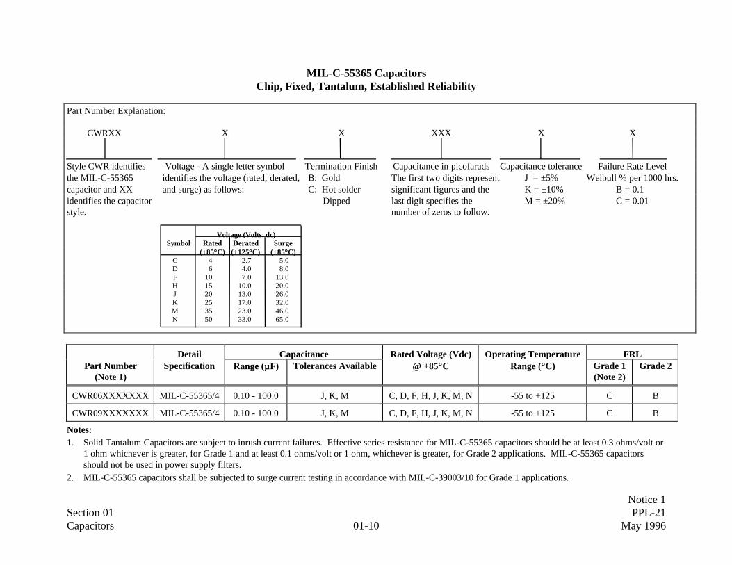
Notice 1Section 01 PPL-21Capacitors 01-10 May 1996
MIL-C-55365 CapacitorsChip, Fixed, Tantalum, Established Reliability
Part Number Explanation:
CWRXX X X XXX X X
Style CWR identifies Voltage - A single letter symbol Termination Finish Capacitance in picofarads Capacitance tolerance Failure Rate Levelthe MIL-C-55365 identifies the voltage (rated, derated, B: Gold The first two digits represent J = ±5% Weibull % per 1000 hrs.capacitor and XX and surge) as follows: C: Hot solder significant figures and the K = ±10% B = 0.1identifies the capacitor Dipped last digit specifies the M = ±20% C = 0.01style. number of zeros to follow.
Voltage (Volts, dc)Symbol Rated Derated Surge
(+85°°C) (+125°°C) (+85°°C)C 4 2.7 5.0D 6 4.0 8.0F 10 7.0 13.0H 15 10.0 20.0J 20 13.0 26.0K 25 17.0 32.0M 35 23.0 46.0N 50 33.0 65.0
Detail Capacitance Rated Voltage (Vdc) Operating Temperature FRLPart Number
(Note 1)Specification Range (µµF) Tolerances Available @ +85°°C Range (°°C) Grade 1
(Note 2)Grade 2
CWR06XXXXXXX MIL-C-55365/4 0.10 - 100.0 J, K, M C, D, F, H, J, K, M, N -55 to +125 C B
CWR09XXXXXXX MIL-C-55365/4 0.10 - 100.0 J, K, M C, D, F, H, J, K, M, N -55 to +125 C B
Notes:1. Solid Tantalum Capacitors are subject to inrush current failures. Effective series resistance for MIL-C-55365 capacitors should be at least 0.3 ohms/volt or
1 ohm whichever is greater, for Grade 1 and at least 0.1 ohms/volt or 1 ohm, whichever is greater, for Grade 2 applications. MIL-C-55365 capacitorsshould not be used in power supply filters.
2. MIL-C-55365 capacitors shall be subjected to surge current testing in accordance with MIL-C-39003/10 for Grade 1 applications.

Notice 1Section 01 PPL-21Capacitors 01-11 May 1996
MIL-C-55681 Capacitors Chip (Page 1 of 2)Multiple Layer, Fixed, Unencapsulated, Ceramic Dielectric, Established Reliability
Part Number Explanation:CDRYY BY XYZ Y Y Y Y
Style - CDR identifies Rated temperature (B) Capacitance in pF. Rated Voltage Capacitance Termination Finish Failure Ratethe MIL-C-55681 and voltage temperature XY = Significant digits (Vdc) Tolerance S = Solder-coated, final Level:capacitor and YY limits (Y) (Note 1) Z = number of zeros A = 50 B = ±0.10pF M = Palladium-silver (% per 1000 hrs)identifies the capacitor B = -55°C to +125°C For values less than B = 100 C = ±0.25pF N = Silver-nickel-gold P = 0.1style. Y = P = 0± 30ppm/°C 10pF, X and Z = C = 200 D = ±0.50pF U = Base Metallization- R = 0.01
Y = X = +15%, -25% Significant digits, D = 300 F = ±1% Barrier Metal- S = 0.001Y = G = 90 ± 20ppm/°C Y = decimal point (R) E = 500 G = ±2% Solder coated
(Note 2) J = ±5%K = ±10%M = ±20%
Capacitance Rated Voltage @ Operating Rated Temperature FRLPart Number Detail
SpecificationStyle Range (pF)
(Note 2)TolerancesAvailable
+125°°C (Vdc)(Note 3)
TemperatureRange (°°C)
& VoltageTemperature Limits
Grade 1(Note 4)
Grade 2
CDR01BYYYYYYYYCDR03BYYYYYYYYCDR04BYYYYYYYY
MIL-C-55681/1CDR01CDR03CDR04
10-4,700330-68,000
1,200,-180,000
J, K, MJ, K, MK, M
10050, 10050, 100
BX, BPBX, BP
BXCDR05BYYYYYYYYCDR06BYYYYYYYY
MIL-C-55681/2MIL-C-55681/3
CDR05CDR06
3,900-330,0006,800-470,000
J, K, MJ, K, M
50, 10050, 100
BX, BPBX, BP
CDR11BYYYYYYYYCDR12BYYYYYYYYCDR13BYYYYYYYYCDR14BYYYYYYYY
MIL-C-55681/4
CDR11CDR12CDR13CDR14
0.1-1,0000.1-1,0000.1-5,1006.8-5,100
B, C, D, FG, J, K, M
5050
50, 100, 200300, 500
-55 to+125
BG, BP
S P, R
CDR31BYYYYYYYY MIL-C-55681/7 CDR31 1.0-18,000 F, J, K, M 50, 100, 200, 300 BX, BPCDR32BYYYYYYYY MIL-C-55681/8 CDR32 1.0-39,000 B, C, D,
F, J, K, M50, 100 BX, BP
CDR33BYYYYYYYY MIL-C-55681/9 CDR33 1,000-100,00 F, J, K, M 50, 100 BX, BPCDR34BYYYYYYYY MIL-C-55681/10 CDR34 2,200-180,000 F, J, K, M 50, 100 BX, BPCDR35BYYYYYYYY MIL-C-55681/11 CDR35 4,700-470,000 F, J, K, M 50, 100 BX, BP
See notes on page 01-12.
Notice 1Section 01 PPL-21Capacitors 01-12 May 1996
MIL-C-55681 Capacitors Chip (Page 2 of 2)Multiple Layer, Fixed, Unencapsulated, Ceramic Dielectric, Established Reliability
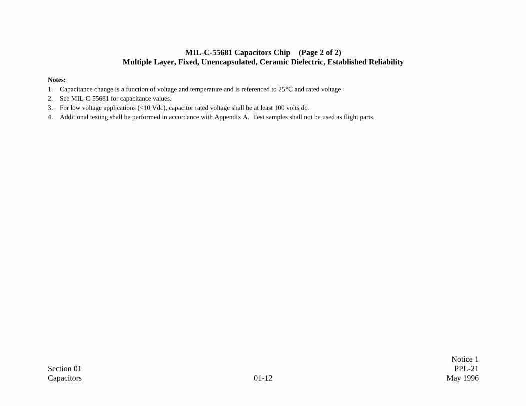
Notes:1. Capacitance change is a function of voltage and temperature and is referenced to 25°C and rated voltage.2. See MIL-C-55681 for capacitance values.3. For low voltage applications (<10 Vdc), capacitor rated voltage shall be at least 100 volts dc.4. Additional testing shall be performed in accordance with Appendix A. Test samples shall not be used as flight parts.

Notice 1Section 01 PPL-21Capacitors 01-13 May 1996
MIL-C-83421 Capacitors (Note 1)Fixed, Metallized Plastic Film Dielectric, Hermetically Sealed, Established Reliability
Part Number Explanation:
M83421 /XX - X XXX X
Military Specification Number Detail Specification Number Style Uniquely specifies the Failure Rate Level:1 = CRH01 capacitance value, (% per 1000 hrs.)2 = CRH02 capacitance tolerance, R = 0.013 = CRH03 ac ratings, and physical S = 0.0014 = CRH04 dimensions of the capacitor5 = CRH05
Capacitance Rated Voltage Dissipation Dielectric Operating FRLPart Number Detail
SpecificationStyle
(Note 2)Range(µµF)
Tolerances(±±%)
@ +100°°C(Vdc)
Factor(% max)
Absorption(% max)
Temperature
Range (°°C)
Grade1
Grade2
M83421/01-XXXXX MIL-C-83421/1
CRH01CRH02CRH03
0.001-22.00.001-10.00.001-10.0 1, 5, 10
3050100 0.15 0.1 -65 to +100 S R
(Note 3) CRH04CRH05
0.001-3.90.001-2.0
200400
Notes:1. These parts shall not be used outside of the limits under INTENDED USE in the notes section of MIL-C-83421. Minimum stored energy in the range 100
to 500 microjoules is recommended to insure clearing. Applications for these capacitors shall be limited to circuits that will provide sufficient energy toinsure clearing and that are insensitive to momentary breakdown/clearing actions.
2. Lead material and coating are specified in MIL-C-83421/1.3. Parts covered by this specification contain internal soldered connections which may reflow during installation. The plastic dielectric in these parts is also
temperature sensitive. Special precautions such as heat sinking are recommended when soldering onto boards.

Notice 1Section 01 PPL-21Capacitors 01-14 May 1996
MIL-C-87217 CapacitorsFixed, Supermetallized Plastic Film Dielectric, Direct Current for Low Energy, High Impedence Applications,
Hermetically Sealed in Metal Cases, High Reliability
Part Number Explanation:
M87217 /XX -X XXX X
Military Specification Number Detail Specification Number Specifies capacitor style Uniquely specifies the A = Sleevedand rated voltage the capacitance value, B = Unsleeved1 = CHS01, 30V tolerance, and dimensions2 = CHS02, 50V3 = CHS03, 100V
Capacitance Rated Voltage Operating TemperaturePart Number Detail
SpecificationStyle
(Note 1)Range(µµF)
Tolerances(±±%)
@ +100°°C(Vdc)
Range(°°C)
Grade
M87217/01-XXXXX(Notes 1, 2)
MIL-C-87217/1CHS01CHS02CHS03
0.001 - 10.00.25, 0.5,1.0, 2.0,
5.0, 10.0
3050100
-55 to +100 (Note 3)
Notes:1. To ensure clearing of breakdown, it is recommended that the circuit in which capacitors of 0.1µF and greater capacitance are intended for use should be
capable of providing at least 100 microjoules of energy.2. Parts covered by this specification contain internal soldered connections which may reflow during installation. The plastic dielectric in these parts is also
temperature sensitive. Special precautions such as heat sinking are recommended when soldering onto boards.3. These parts may be used in Grade 1 and Grade 2 applications.

Notice 1Section 02 PPL-21Connectors 02-1 May 1996
Summary of Preferred Connectors (Note 1) (Page 1 of 2)
Type Designation Description Specification Grade Refer ToPage No.
NLS Circular, High Density, Miniature, Low Outgassing MSFC 40M38277 1, 2 02-3NBS Circular, Miniature, Low Outgassing MSFC 40M38298 1, 2 02-4NB Circular, Miniature, Low Outgassing MSFC 40M39569 1, 2 02-5MS27XXX Circular, Miniature, Series I, Bayonet Coupled MIL-C-38999 1, 2 02-7MS27XXX Circular, Low Silhouette, Miniature, Series II (Note 2) MIL-C-38999 1, 2 02-7D38999/XX Circular, Miniature, Series III, Self Locking Coupling MIL-C-38999 1, 2 02-9D38999/XX Circular, Miniature, Series IV, Breech Coupling MIL-C-38999 1, 2 02-9MS34XX Circular, Miniature, Series 2 (Notes 3, 4) MIL-C-26482 2 02-11MS345X Circular, Crimp Rear Release Contacts (Note 4) MIL-C-5015 2 02-13311P409 D-Subminiature Type, Removal Crimp Contacts, Low Residual Magnetism GSFC S-311-P-4/09 1, 2 02-14, 02-17311P407 D-Subminiature Type, High Density, Crimp Removable Contacts, Low
Residual MagnetismGSFC S-311-P-4/07 1, 2 02-14, 02-18
311P405 D-Subminiature Type, Combination Power, Coaxial and High VoltageContacts, Low Residual Magnetism
GSFC S-311-P-4/05 1, 2 02-14, 02-20
311P10 D-Subminiature Type, Solder Contacts, Low Residual MagnetismStandard Power and Combination Inserts
GSFC S-311-P-10 1, 2 02-15, 02-19,02-20
M24308/XX D-Type Subminiature Solder or Removable Crimp Contacts (Note 5) MIL-C-24308 2 02-16, 02-17,02-18, 02-19
M55302/XX Printed Circuit MIL-C-55302 2 02-21M39012/XX Coaxial, Radio Frequency, Series SMA (Note 6) MIL-C-39012 2 02-24M83517/X Transmission Line, Radio Frequency, Series SMA MIL-C-83517 2 02-27M83513/XX Microminiature, Pre-Terminated Crimp or Solder Contacts MIL-C-83513 2 02-29M83513/XX Microminiature, Printed Circuit Connectors MIL-C-83513 2 02-30700-42 Power Connectors, Satellite Interface, Crimp Removable Contacts GSFC S-311-P-718 1, 2 02-31M39029/XX Contacts, Electrical Connector MIL-C-39029 2 02-37M85049/XX Backshell Connector Accessories MIL-C-85049 1, 2 02-39
See notes on page 02-2.

Notice 1Section 02 PPL-21Connectors 02-2 May 1996
Index of Preferred Connectors (Note 1) (Page 2 of 2)
Notes:1. The use of connectors with cadmium or zinc plating, which tends to sublimate in a vacuum, is prohibited. Gold over nickel or electroless nickel are the
preferred platings for GSFC applications. For contacts, gold plating with a 50 microinch thickness over the engagement area is the GSFC preferred finish.2. Use MSFC NLS type as first choice where low outgassing is a requirement.3. Use MSFC NB type as first choice where low outgassing is a requirement.4. For circular connectors were outgassing is not a concern, use MIL-C-38999 connectors as a first choice. Use MIL-C-5015 where large contacts and high
currents are a requirement.5. Use GSFC S-311-P-4 or S-311-P-10 for first choice were low residual magnetism is a requirement.6. MIL-C-39012 Series N and TNC are not preferred parts for GSFC programs due to concerns with atomic oxygen corrosion of the silver plating when used
in earth orbits.

Notice 1Section 02 PPL-21Connectors 02-3 May 1996
MSFC 40M38277 Circular Connectors, High Density, (Notes 1 and 2)Low Silhouette, Low Outgassing, Bayonet Coupled, -150°C to +200°C
Part Number Explanation:
NLS X(X) X X(X) —35 X(X) X
Series Prefix Shell Style Class (Seal) Shell Size Arrangement Number Contact Type Insert Polarization(Table 02-3-1) E = Environmental with P = Pins
straight compression S = Sockets (Blank) = Normal ring backshell Insert Arrangement PS = Pin Socket A, B, C, D =H = Hermetic (Note 3) (Table 02-3-3) Feed thru Alternate PositionsT = Environmental without (Note 5) (Style 5 only) backshell (Note 4) (Table 02-3-2)
Table 02-3-1 Connector Styles Table 02-3-2 Table 02-3-3
Notes:1. Connectors may be used in Grade 1 and 2 applications.2. Connectors are supplied with contacts.3. Temperature range for hermetically sealed connectors is
-100°C to +150°C.4. Backshell strain relief must be procured separately for
Class T connectors.5. Insert arrangement designation consists of shell size and
arrangement number. For 40M38277 connectors, only size 22D contacts are available.
0 = Receptacle flange mount 6 = Plug, cable mount
3 = Receptacle, solder mount hermetic
6G = Plug, cable mount with RFI Grounding finders
5 = Bulkhead feedthrough, hermetic jam nut mount (Double sided connector)
6W = Plug, cable mount, without coupling ring& backshell7 = Receptacle, jam nutmount
Backshells for 40M38277Class T Connectors
Part Number Explanation:NLS X(XX) X(X) X(X)
Series Style Shell ClampPrefix Size 8 Size
thru 24 1 thru 16(Style RFI
only)
S = Straight with strain relief clampR = Right angle with strain relief clampC = Straight compression ringSCT = Straight with cable tie strain reliefRCT = Right angle with cable tie strain reliefFCT = 45° angle with cable tie strain reliefRFI = Straight RFI shield termination.
Insert No. of ContactsArrangement (All size 22D)
8 - 35 610 - 35 1312 - 35 2214 - 35 3716 - 35 5518 - 35 6620 - 35 7922 - 35 10024 - 35 128

Notice 1Section 02 PPL-21Connectors 02-4 May 1996
MSFC 40M38298 Circular Connectors, Miniature, (Note 1)Low Outgassing, Bayonet Coupled, -150°C to +200°C
Part Number Explanation:NBS X(X) X 8 —X X X
Series Prefix Shell Style Class (Seal) Shell Size Arrangement Number Contact Type Insert Polarization(Table 02-4-1) E = Environmental P = Pins N = Normal
H = Hermetic S = Sockets A through H =(Note 2) Insert Arrangement Alternate Positions
(Table 02-4-3)Table 02-4-1 Connector Styles Table 02-4-2 Table 02-4-3 (Note 7)
Notes:1. Connectors may be used in Grade 1 and Grade 2 applications. They are supplied with contacts.2. Temperature range for hermetically sealed connectors is -100°C to +150°C.3. When styles 6, 6G and 7, are used in space shuttle missions, only polarization N, A, B, C, D shall be used.4. For style 6, 6G and 7, procure strain relief backshell separately. See Table 02-4-2.5. When styles 9 and 9G, are used in space shuttle missions, insert arrangement 8-2 with socket contacts and E, F, G & H polarization shall be reserved for connection to NSI-
1 (NASA standard initiator Type 1) pyrotechnic firing circuits.6. Crimp type ferrule is required to terminate cable shield to the backshell, and must be provided separately. Order Thomas & Betts P/N GSC 17512NP or equivalent.7. Insert arrangement designation consists of shell size and arrangement number. For 40M38298 connectors, only size 20 contacts ar e available.
0 = Receptacle,flange mounthermetic
6G = Plug, cable mountwith RFIgrounding fingers(Notes 3, 4)
8G = Plug, cablemount, withright angle RFIbackshell andRFI groundingfingers
3 = Receptacle,surface mounthermetic
7 = Receptacle, jamnut mount(Notes 3, 4)
9 = Plug withstraight RFIbackshell(Notes 5, 6)
6 = Plug, cablemount(Notes 3, 4)
8 = Plug cable mount,with right angleRFI backshell
9G = Plug withstraight RFIbackshell andRFI groundingfingers(Notes 5, 6)
Backshells for 40M38298Connectors (Styles 6, 6G & 7) (Note 4)
Part Number Explanation:NBS X(XX) 8
Series Style Shell SizePrefix (Use 8R with RFI
Style only for 90°RFI backshell)
S = Straight with strain relief clampR = Right Angle with strain relief clampC = Straight compression ringRFI = Straight RFI shield termination. (Note 6)
Insert No. of ContactsArrangement (All size 20)
8 - 2 28 - 3 38 - 4 4

Notice 1Section 02 PPL-21Connectors 02-5 May 1996
MSFC 40M39569 Circular Connectors, (Notes 1 through 3) (Page 1 of 2)Low Outgassing, Bayonet Coupled, -150°C to +200°C
Part Number Explanation:
NB X(X) X X(X) —X(X) X(X) X X X
Series Prefix Shell Style Class (Seal) Shell Size Arrangement Number Contact Type Insert Polarization Backshell Temp(Table 02-5-1) E = Environmental (Table 02-5-2) N = Normal Accessory Class
H = Hermetic W, X, Y, Z = (N/AHermetics) (Table
(Note 4) Insert Arrangement Alternate Positions (Table 02-5-3) 02-5-4)(Table 02-6-1)
Table 02-5-1 Connector Styles Table 02-5-2 Contacts Table 02-5-3 Backshells Table 02-5-4 Temperature
See notes on page 02-6.
0 = Receptacle, 6 = Plug, cableflange mount mountNarrow
3 = Receptacle, 6G = Plug, cableSolder Mount, mount, withHermetic RFI grounding
fingers4 = Receptacle 7 = Receptacle,
Flange Mount, jam nut mountWide flange
5 = Bulkhead feed 8 = Receptacle, jamthru, hermetic, nut mount,jam nut mount extended pin
P = PinsS = SocketsCP = Coaxial PinCS = Coaxial SocketPS = Pin-Socket feedthrough
(Style 5 only)
C = Straight, compression ringS = Straight, with cable clampR = Right Angle, cable clampT = No backshell
Blank = Gen’l Purpose(-100°C to +200°C)
2 = Vacuum thermal cycled(-150°C to +200°C)
3 = Atmosphere Thermal cycled(-150°C to +200°C)

Notice 1Section 02 PPL-21Connectors 02-6 May 1996
MSFC 40M39569 Circular Connectors, (Notes 1 and 2) (Page 2 of 2)Low Outgassing, Bayonet Coupled, -150°C to +200°C
Table 02-6-1 Insert Arrangements for 40M39569 Connectors (Note 3)
Insert No. of Contacts (By Contact Size) Insert No. of Contacts (By Contact Size)
Arrangement 20 16 12 Coax Arrangement 20 16 12 Coax
8-98 3 18-8 810-6 6 18-11 1112-3 3 18-30 29 112-8 8 18-32 32
12-10 10 20-16 1614-4 4 20-39 37 214-5 5 20-41 41
14-12 8 4 22-12 1214-15 14 1 22-21 2114-18 18 22-41 27 1414-19 19 22-55 5516-8 8 24-19 19
16-23 22 1 24-31 3116-26 26 24-61 61
24-100 8
Notes:1. Connectors may be used in Grade 1 or 2 applications.2. Connectors are supplied with contacts.3. Insert arrangement designation consists of shell size and arrangement number. For 40M39569 connectors, insert arrangements with a variety of contact
sizes are available.4. Temperature range for hermetically sealed connectors is -100°C to +150°C.

Notice 1Section 02 PPL-21Connectors 02-7 May 1996
MIL-C-38999 Series I & II, (Notes 1 through 4) (Page 1 of 2)Circular Connectors, Bayonet Coupled, -65°C to +200°°C
Part Number Explanation:
MS27XXX X X(X) X —X(X) X X
Military Specification Class (Note 5) Shell Size Finish Arrangement Number Contact Type Insert PolarizationNumber T = Environmental (Table 02-7-2) (Note 6) Blank = Normal
(Table 02-7-1) without backshell All Styles A, B, C, D = (N/A MS27508) P = Pin S = Socket Alternate PositionsE = Environmental Insert Arrangement Resisting (Table 02-8-1) Hermetic Alternate Styles (MS27508 only) Y = Pins with eyeletY = Hermetic Z = Sockets with eyelet
Table 02-7-1 Connector Styles Table 02-7-2 GSFC Preferred Finish
Notes: (Continued on page 02-8)1. Connectors require additional processing for contamination control due to outgassing. Special low outgassing Series I and II connectors may be procured
to GSFC Specification S-311-P-768.2. Connectors may be used in Grade 1 and 2 applications.3. Accessories such as strain relief backshells must be provided separately. Refer to Page 02-40 for a selection list.4. Series I and Series II connectors are not intermateable.5. Specify Class T for all type except hermetic and MS27508 connectors. Specify Class E for MS27508 only. Class E is not preferred for all other
specifications and is inactive for new design.6. Connectors are supplied with contacts. Refer to Page 02-37 for a selection of replacement contact part numbers.
CLASS T, EF = Electroless Nickel
CLASS YD = Tin (150°C)E = Passivated Stainless Steel
Series IScoop-Proof
Series IILow Silhouette Style Description
MS27466MS27468MS27656
——
MS27467
MS27472MS27474MS27497MS27508MS27473MS27484
Receptacle, Wall Mount FlangeReceptacle, Jam Nut MountReceptacle, Wall Mount, Back Panel MountReceptacle, Box Mount, Back Panel MountPlugPlug with RFI Grounding Fingers
MS27470MS27471
MS27477MS27478
Receptacle, Jam Nut Mount, HermeticReceptacle, Solder Mount, Hermetic

Notice 1Section 02 PPL-21Connectors 02-8 May 1996
MIL-C-38999 Series I & II, (Page 2 of 2)Circular Connectors, Bayonet Coupled, -65°C to +200°°C
Table 02-8-1 Insert Arrangements for MIL-C-38999 Series I & II Connectors (Notes 7, 8)
Insert Arrangement No. of Contacts (By Contact Size) Insert Arrangement No. of Contacts (By Contact Size)
Series I Series II 22D 20 16 12 Series I Series II 22D 20 16 12
9-35 8-35 6 9-11 18-11 119-98 8-98 3 N/A 18-28 26 211-4 N/A 4 N/A 18-30 29 111-5 10-5 5 19-32 18-32 32
11-35 10-35 13 19-35 18-35 6611-98 10-98 6 N/A 18-96 911-99 10-99 7 21-11 N/A 11N/A 12-3 3 21-16 20-16 1613-4 12-4 4 21-35 20-35 7913-8 12-8 8 21-39 20-39 37 2
13-35 12-35 22 21-41 20-41 4113-98 12-98 10 23-21 22-21 2115-5 14-5 5 N/A 22-32 32
15-15 14-15 14 1 23-35 22-35 10015-18 14-18 18 23-53 N/A 5315-19 N/A 19 23-55 22-55 5515-35 14-35 37 25-4 24-4 48 815-97 14-97 8 4 25-19 24-19 1917-6 16-6 6 25-24 24-24 12 1217-8 16-8 8 25-29 24-29 29
17-26 16-26 26 25-35 24-35 12817-35 16-35 55 25-43 N/A 23 2017-99 16-99 21 2 25-61 24-61 61
Notes:7. Consult latest MIL-C-38999 Qualified Products List for availability. Other insert arrangements are available but are not preferred due to limited
availability.8. Insert arrangement designation consists of shell size and arrangement number. Inserts with a variety of contact sizes are available.

Notice 1Section 02 PPL-21Connectors 02-9 May 1996
MIL-C-38999 Series III & IV, (Notes 1 through 5) (Page 1 of 2)Circular Connectors, -65°C to +200°°C
Part Number Explanation:
D38999/XX X X XX Contact Type (Note 4) X
Military Specification Class Shell Size Arrangement Number All Styles Insert PolarizationNumber (Table 02-9-2) P = Pin N = Normal
(Table 02-9-1) S = Socket A, B, C, D, E =Hermetic Alternate Styles Alternate Positions
Insert Arrangement Y = Pins with eyelets (E N/A Series IV)(Page 02-10) Z = Sockets with eyelets
Table 02-9-1 Connector Detail Specifications Table 02-9-2
Notes: (Continued on page 02-10)1. Connectors require additional processing for contamination control due to outgassing. Special low outgassing Series III connectors may be procured to
GSFC Specification S-311-P-768.2. Connectors may be used in Grade 1 and 2 applications.3. Accessories such as strain relief backshells must be provided separately. Refer to Page 02-40 for a selection list.4. Connectors are supplied with contacts. Refer to Page 02-37 for a selection of replacement contact part numbers.5. Series III and Series IV connectors are not intermateable, nor are they intermateable with Series I or II.
CLASS DESCRIPTION
F = Environment Resisting, Conductive Electroless Nickel CoatingN = Hermetically Sealed, Corrosion Resistant Steel, Conductive Electro- Deposited Nickel FinishY = Hermetically Sealed, Corrosion Resistant Steel, Conductive Passivated Finish
Series IIIScoop-Proof
3 Way Self LockingThreaded Coupling
Series IVScoop Proof
Breech CouplingStyle Description
D38999/20D38999/24
——
D38999/26
D38999/40D38999/44D38999/42D38999/47D38999/46
Receptacle, Wall Mount FlangeReceptacle, Jam Nut MountReceptacle, Box MountPlugPlug, EMI Grounding Fingers
D38999/21D38999/23D38999/25D38999/27
D38999/41D38999/43D38999/45D38999/48
Receptacle, Box Mount, HermeticReceptacle, Jam Nut Mount, HermeticReceptacle, Solder Mount, HermeticReceptacle, Weld Mount, Hermetic

Notice 1Section 02 PPL-21Connectors 02-10 May 1996
MIL-C-38999 Series III & IV, (Page 2 of 2)Circular Connectors, -65°C to +200°°C
Table 02-10-1 Insert Arrangements for MIL-C-38999 Series III & IV Connectors (Notes 6, 7)
Insert Arrangement No. of Contacts (ByContact Size)
Insert Arrangement No. of Contacts (ByContact Size)
Number Series III Series IV 22D 20 16 12 Number Series III Series IV 22D 20 16 12
A35 X N/A 6 F11 X X 11A98 X N/A 3 F32 X X 32B4 X N/A 4 F35 X X 66B5 X X 5 G11 X X 11B35 X X 13 G16 X X 16B98 X N/A 6 G35 X X 79B99 X X 7 G39 X N/A 37 2C4 X X 4 G41 X X 41C8 X N/A 8 H21 X X 21
C35 X X 22 H35 X X 100C98 X X 10 H53 X N/A 53D5 X X 5 H55 X X 55
D15 X N/A 14 1 J4 X X 48 8D18 X X 18 J19 X X 19D19 X X 19 J24 X X 12 12D35 X X 37 J29 X X 29D97 X X 8 4 J35 X X 128E6 X X 6 J43 X N/A 23 20E8 X X 8 J61 X X 61
E26 X X 26E35 X X 55E99 X X 21 2
Notes:6. Insert arrangement designation consists of shell size designator and arrangement number. Insert arrangements with a variety of contact sizes are available.
Insert arrangement shell size designations are as follows: A=Shell size 9, B=11, C=13, D=15, E=17, F=19, G=21, H=23, J=257. Consult latest MIL-C-38999 Qualified Products List for availability. Other insert arrangements are available but are not preferred due to limited QPL
availability.

Notice 1Section 02 PPL-21Connectors 02-11 May 1996
MIL-C-26482 Series 2, Circular Connectors, (Notes 1 through 4) (Page 1 of 2)Bayonet Coupled, -55°C to +200°°C
Part Number Explanation:
MS34XX X X(X) — X(X) X (X)
Military Specification Class Shell Size (Note 5) Arrangement Number Contact Type Insert(Table 02-11-1) (Table 02-11-2) (Note 4) Polarization
P = Pin Blank = NormalInsert Arrangement S = Socket W, X, Y, Z =(Table 02-12-1) Alternate
Positions
Table 02-11-1 Configuration Styles Table 02-11-2 Class Table 02-11-3 MS3449 Termination Type
Notes: (Continued on page 02-12)1. Connectors require additional processing for contamination control due to outgassing. Special low outgassing connectors may be procured to GSFC
Specification S-311-P-768.2. Connectors are preferred for Grade 2 applications where outgassing is not a concern. Consult Appendix A for additional testing required in Grade 1.3. Accessories such as strain relief backshells must be provided separately. Refer to Page 02-40 for a selection list.4. Connectors are supplied with contacts. Refer to Page 02-37 for a selection of replacement contact part numbers.5. For MS3449 Hermetic Connectors, replace the “—” with the code designation from Table 02-11-3 to specify solder contact terminations types. Only pin
type contacts are available with hermetic connectors.
L = Fluid Resistant, Electroless Nickel Finish (Preferred)A = Grommet Seal, Non-Conductive Anodic Coating (Not for use with MS3475 Plug)H = Hermetic Seal, Steel Shell, Tin over Nickel Finish or stainless steel shell, passivated
MS3470 = Receptacle, Flange Mount, Narrow Flange
MS3472 = Receptacle, Flange Mount, Wide Flange
MS3474 = Receptacle, Jam Nut Mount
MS3475 = Plug, Cable Mount, RFI Shielded
MS3476 = Plug, Cable Mount
MS3449 = Receptacle, Hermetic
Code Description Shell Mat’lA
B
C
Solder cup
Eyelet
Soldercup
Stainless Steel
Stainless Steel
Cold Rolled Steel

Notice 1Section 02 PPL-21Connectors 02-12 May 1996
MIL-C-26482 Series 2, Circular Connectors, (Page 2 of 2)Bayonet Coupled, -55°C to +200°°C
Table 02-12-1 Insert Arrangements for MIL-C-26482 Connectors (Notes 6, 7)Insert No. of Contacts (By Contact Size) Insert No. of Contacts (By Contact Size)
Arrangement 20 16 12 Arrangement 20 16 128-33 3 18-8 88-98 3 18-11 1110-6 6 18-30 29 112-3 3 18-32 3212-8 8 20-16 1612-10 10 20-24 2414-4 4 20-39 37 214-5 5 20-41 4114-9 5 4 22-12 1214-12 8 4 22-21 2114-15 14 1 22-32 3214-18 18 22-41 27 1414-19 19 22-55 5516-8 8 22-95 26 616-14 8 6 24-19 1916-23 22 1 24-31 31
24-61 61Notes:6. Insert arrangement designation consists of shell size designator and arrangement number. Insert arrangements with a variety of contact sizes are available.7. Consult latest MIL-C-26482 qualified products list for availability. Other insert arrangements are available but are not preferred due to limited
availability.

Notice 1Section 02 PPL-21Connectors 02-13 May 1996
MIL-C-5015, Circular Connectors, (Notes 1 through 4)Threaded Coupling, Rear Release Contacts, -55°C to +200°°C
Part Number Explanation:
MS345X L — XX (X)X(X) X X
Military Specification Class Material Designator Shell Size Arrangement Number Contact Type InsertNumber L = Fluid Resistant Blank = Aluminum P = Pin Polarization
(Table 02-13-1) Electroless Nickel Alloy S = Socket Blank = NormalFinish Insert Arrangement W, X, Y, Z =
(Table 02-13-2) Alternate Positions
Table 02-13-1 Connector Styles (Note 5) Table 02-13-2 PreferredMIL-C-5015 Insert Arrangements (Note 6)
Notes:1. Connectors require additional processing for contamination control due to outgassing.2. Connectors are preferred for Grade 2. Consult Appendix A for additional testing required
in Grade 1 applications.3. Connectors are supplied with contacts. Refer to Page 02-37 for a selection of replacement
contact part numbers.4. Accessories such as strain relief backshells must be provided separately. Refer to Page 02-40
for a selection list.5. These MIL-C-5015 connectors supersede MIL-C-83723 Series II connectors per
MIL-C-83723/19 through MIL-C-83723/24. MS345X connectors are fully intermateable andintermountable with MIL-C-83723 Series II connectors.
6. Insert arrangement designation consists of shell size designator and arrangement number.Insert arrangements with a variety of contacts sizes are available. Only GSFC preferred insertarrangements are shown. Other insert arrangements are available. Consult latest MIL-C-5015Qualified Products List for availability.
MS3450 = Receptacle, Wall Mount MS3456 = Plug, Cable Mount
MS3452 = Receptacle, Box Mount MS3459 = Plug, Cable Mount, Self (No Provision for backshell Locking Coupling Ring Attachment)
MS3454 = Receptacle, Jam Nut Mount
Number of Contacts (By Contact Size)Insert Arrangement 16 12 8 4 0
14S2 (Short Shell)14S5 (Short Shell)14S7 (Short Shell)16S1 (Short Shell)
18-120-420-2722-222-1422-2224-1024-2828-2132-1736-536-1036-52
453710
14
19
2437
4852
4
3
47
44

Notice 1Section 02 PPL-21Connectors 02-14 May 1996
GSFC S-311-P-4 D-Subminiature Connectors, Crimp Removable Contacts, -55°C to +125°C (Notes 1 through 4)
Part Number Explanation:
311P4 0X -X X -X -XX
GSFC Procurement Detail Specification Insert Arrangement Contact Type Residual Magnetism Mounting Hole SizeSpecification Prefix 09 = Standard Density S = Sockets Level 12 = .120 in
(Size 20 contacts, P = Pins B = 200 Gamma 15 = .150 in (Page 02-17)07 = High Density (Size 22D contacts) Page 02-18)05 = Combination Inserts (Note 5)
Notes:1. a. 311P409 connectors are described in detail on page 02-17 and are compared with MIL-C-24308 connectors with size 20 crimp contacts.
b. 311P407 connectors are described in detail on page 02-18 and are compared with MIL-C-24308 connectors with size 22D crimp contacts.c. 311P405 connectors and insert arrangements are described in detail on page 02-20.
2. Connectors may be used in Grade 1 and Grade 2 applications.3. Hardware such as screwlocks, jackscrews, and jackposts are required to properly secure mated connector pairs, and must be provided separately. Non-
magnetic hardware is recommended to maintain controlled residual magnetism.4. Connectors satisfy GSFC outgassing requirements of 1 percent Total Mass Loss (TML) and 0.1 percent Collected Volatile Condensable Material (CVCM).5. Connectors are offered with combination type inserts which offer a variety of insert arrangements for use with coaxial and high voltage contacts with No.
20 power contacts. Insert arrangements and contact part numbers are given on page 02-20.

Notice 1Section 02 PPL-21Connectors 02-15 May 1996
GSFC S-311-P-10 D-Subminiature Connectors, Solder Contacts, -55°C to +125°C (Notes 1 through 4)
Part Number Explanation:
311P10 (B) -X X -X -XX
GSFC Procurement Socket Contact Designator Insert Arrangement Contact Type Residual Magnetism Mounting Hole SizeSpecification Prefix (Not applicable to pin contacts) Page 02-19 for P = Pins Level 12 = .120 inch
No digit = contact springs Standard Density. S = Sockets B = 200 Gamma 15 = .150 inchB = split finger sleeved Page 02-20 for C = 20 Gamma
(first choice) combination insertarrangements.
Notes:1. 311P10 connectors with insert arrangements 1 through 5 are described in detail on page 02-19, and are compared with equivalent MIL-C-24308
connectors with size 20 solder contacts. 311P10 connectors with insert arrangements 6 through 25 are shown in detail on page 02-20, and are compared toequivalent 311P405 combination insert connectors.
2. Connectors may be used in Grade 1 or Grade 2 applications.3. Hardware such as screwlocks, jackscrews, and jackposts are required to properly secure mated connector pairs, and must be provided separately. Non-
magnetic hardware is recommended to maintain controlled residual magnetism.4. Connectors satisfy GSFC outgassing requirements of 1 percent Total Mass Loss (TML) and 0.1 percent Collected Volatile Condensable Material (CVCM).
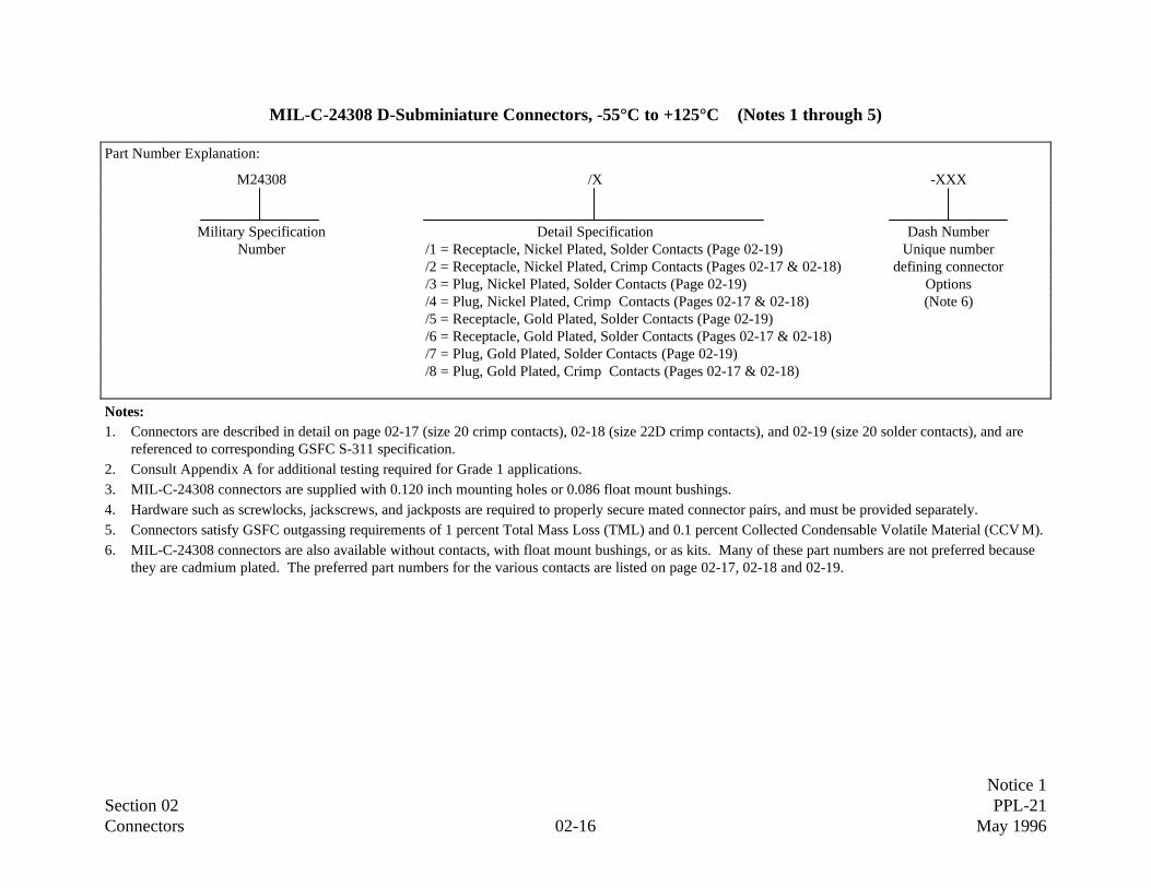
Notice 1Section 02 PPL-21Connectors 02-16 May 1996
MIL-C-24308 D-Subminiature Connectors, -55°C to +125°C (Notes 1 through 5)
Part Number Explanation:
M24308 /X -XXX
Military Specification Detail Specification Dash NumberNumber /1 = Receptacle, Nickel Plated, Solder Contacts (Page 02-19) Unique number
/2 = Receptacle, Nickel Plated, Crimp Contacts (Pages 02-17 & 02-18) defining connector/3 = Plug, Nickel Plated, Solder Contacts (Page 02-19) Options/4 = Plug, Nickel Plated, Crimp Contacts (Pages 02-17 & 02-18) (Note 6)/5 = Receptacle, Gold Plated, Solder Contacts (Page 02-19)/6 = Receptacle, Gold Plated, Solder Contacts (Pages 02-17 & 02-18)/7 = Plug, Gold Plated, Solder Contacts (Page 02-19)/8 = Plug, Gold Plated, Crimp Contacts (Pages 02-17 & 02-18)
Notes:1. Connectors are described in detail on page 02-17 (size 20 crimp contacts), 02-18 (size 22D crimp contacts), and 02-19 (size 20 solder contacts), and are
referenced to corresponding GSFC S-311 specification.2. Consult Appendix A for additional testing required for Grade 1 applications.3. MIL-C-24308 connectors are supplied with 0.120 inch mounting holes or 0.086 float mount bushings.4. Hardware such as screwlocks, jackscrews, and jackposts are required to properly secure mated connector pairs, and must be provided separately.5. Connectors satisfy GSFC outgassing requirements of 1 percent Total Mass Loss (TML) and 0.1 percent Collected Condensable Volatile Material (CCVM).6. MIL-C-24308 connectors are also available without contacts, with float mount bushings, or as kits. Many of these part numbers are not preferred because
they are cadmium plated. The preferred part numbers for the various contacts are listed on page 02-17, 02-18 and 02-19.

Notice 1Section 02 PPL-21Connectors 02-17 May 1996
GSFC S-311-P-4/09 and MIL-C-24308 D-Subminiature ConnectorsStandard Density Size 20 Crimp Contacts (Note 1)
Description
Shell Finish
Grade
General Purpose
Nickel
2
Non-Magnetic
Gold
2
Non-Magnetic Controlled LowResidual Magnetism
Gold
1 and 2Specification MIL-C-24308/2 MIL-C-24308/6 GSFC S-311-P-4/09
Number of Contacts(All Size 20)
Part Number(Note 2)
Part Number(Note 2)
Part Number(Note 3)
Receptacle,Socket
Contacts
915253750
M24308/2-516M24308/2-517M24308/2-518M24308/2-519M24308/2-520
M24308/6-502M24308/6-503M24308/6-504M24308/6-505M24308/6-506
311P409-1S-B-12311P409-2S-B-12311P409-3S-B-12311P409-4S-B-12311P409-5S-B-12
Specification MIL-C-24308/4 MIL-C-24308/8 GSFC S-311-P-4/09
Number of Contacts(All Size 20)
Part Number(Note 2)
Part Number(Note 2)
Part Number(Note 3)
Plug,Pin
Contacts
915253750
M24308/4-335M24308/4-336M24308/4-337M24308/4-338M24308/4-339
M24308/8-335M24308/8-336M24308/8-337M24308/8-338M24308/8-339
311P409-1P-B-12311P409-2P-B-12311P409-3P-B-12311P409-4P-B-12311P409-5P-B-12
Notes:1. The following MIL-C-24308 numbers are also preferred parts for Grade 2 applications:
M24308/2 -521 to -525 (kit); -560 to -564 (less contacts); -585 to -589, -596 to -600, -607 to -611 (.086 DIA float mount bushings in lieu of .120 DIAmounting holes).M24308/4 -340 to -344 (Kit), -357 to -361 (less contacts), -401 to -405, -412 to -416, -423 to -427 (float mount).M24308/6 -507 to -511 (Kit), -540 to -544 (less contacts), -551 to -555, -562 to -566, -573 to -577 (float mount).M24308/8 -340 to -344 (Kit), -357 to -361 (less contacts), -401 to -405, -412 to -416, -423 to -427 (float mount).
2. MIL-C-24308 Connectors are supplied with contacts. Replacement contact part numbers are M39029/63-368 for sockets and M24308/64-367 for pins.3. GSFC connectors are supplied without contacts. Procure P/N G10S1 for socket contacts and G10SP1 for pin contacts per GSFC specification S-311-P -
4/10.

Notice 1Section 02 PPL-21Connectors 02-18 May 1996
GSFC S-311-P-4/07 and MIL-C-24308 D-Subminiature ConnectorsHigh Density Size 22D Crimp Contacts (Note 1)
Description
Shell Finish
Grade
General Purpose
Nickel
2
Non-Magnetic
Gold
2
Non-Magnetic Controlled LowResidual Magnetism
Gold
1 and 2Specification MIL-C-24308/2 MIL-C-24308/6 GSFC S-311-P-4/07
Number of Contacts(All Size 22D)
Part Number(Note 2)
Part Number(Note 2)
Part Number(Note 3)
Receptacle,Socket
Contacts
1526446278104
M24308/2-526M24308/2-527M24308/2-528M24308/2-529M24308/2-530M24308/2-531
M24308/6-512M24308/6-513M24308/6-514M24308/6-515M24308/6-516M24308/6-517
311P407-1S-B-12311P407-2S-B-12311P407-3S-B-12311P407-4S-B-12311P407-5S-B-12311P407-6S-B-12
Specification MIL-C-24308/4 MIL-C-24308/8 GSFC S-311-P-4/07
Number of Contacts(All Size 22D)
Part Number(Note 2)
Part Number(Note 2)
Part Number(Note 3)
Plug,Pin
Contacts
1526446278104
M24308/4-345M24308/4-346M24308/4-347M24308/4-348M24308/4-349M24308/4-350
M24308/8-345M24308/8-346M24308/8-347M24308/8-348M24308/8-349M24308/8-350
311P407-1P-B-12311P407-2P-B-12311P407-3P-B-12311P407-4P-B-12311P407-5P-B-12311P407-6P-B-12
Notes:1. The following MIL-C-24308 numbers are also preferred parts for Grade 2 applications:
M24308/2 -532 to -537 (Kit); -565 to -570 (less contacts); -590 to -595, -601 to -606, -612 to -617 (.086 DIA float mount bushings in lieu of .120 DIA mounting holes).M24308/4 -351 to -356 (Kit), -362 to -367 (less contacts), -406 to -411, -417 to -422, -428 to -433 (float mount).M24308/6 -518 to -523 (Kit), -545 to -550 (less contacts), -556 to -561, -567 to -572, -578 to -583 (float mount).M24308/8 -351 to -356 (Kit), -362 to -367 (less contacts), -406 to -411, -417 to -422, -428 to -433 (float mount).
2. MIL-C-24308 Connectors are supplied with contacts. Replacement contact part numbers are M39029/57-354 for sockets and M24308/58-360 for pins.3. GSFC connectors are supplied without contacts. Procure P/N G08S1 for socket contacts and G08P1 for pin contacts per GSFC specification S-311-P-4/08.

Notice 1Section 02 PPL-21Connectors 02-19 May 1996
GSFC S-311-P-10 and MIL-C-24308 D-Subminiature Connectors, Standard Density Size 20 Solder Contacts (Note 1)
Description
Shell Finish
Grade
General Purpose
Nickel
2
Non-Magnetic
Gold
2
Non-Magnetic Controlled LowResidual Magnetism
Gold
1 and 2Specification MIL-C-24308/1 MIL-C-24308/5 GSFC S-311-P-10
Number of Contacts(All Size 20)
Part Number Part Number Part Number
Receptacle,Socket
Contacts
915253750
M24308/1-34M24308/1-35M24308/1-36M24308/1-37M24308/1-38
M24308/5-34M24308/5-35M24308/5-36M24308/5-37M24308/5-38
311P10-1S-B-12311P10-2S-B-12311P10-3S-B-12311P10-4S-B-12311P10-5S-B-12
Specification MIL-C-24308/3 MIL-C-24308/7 GSFC S-311-P-10
Number of Contacts(All Size 20)
Part Number Part Number Part Number
Plug,Pin
Contacts
915253750
M24308/3-23M24308/3-24M24308/3-25M24308/3-26M24308/3-27
M24308/7-23M24308/7-24M24308/7-25M24308/7-26M24308/7-27
311P10-1P-B-12311P10-2P-B-12311P10-3P-B-12311P10-4P-B-12311P10-5P-B-12
Notes:1. The following part number which offer .086 diameter float mount bushings in lieu of .120 diameter mounting holes are also preferred connectors for Grade
2 applications: M24308/1 -56 through -60; M24308/3-39 through -43; M24308/5-56 through -60; M24308/7-34 through -38.

Notice 1Section 02 PPL-21Connectors 02-20 May 1996
GSFC S-311-P-4/05 and S-311-P-10 D-Subminiature Connectors, (Notes 1 and 2)Combination Power, Coaxial and High Voltage Contacts
Table 02-20-1 Insert Arrangements Table 02-20-2 Coaxial and High Voltage Contact Part Numbers
Notes:1. Coaxial contacts should be used for signals of 1 Mhz frequency or less. Use MIL-C-39012 connectors for higher frequencies.2. Some suppliers use a nylon insulator material in their high voltage contacts. The nylon insulator may not meet program outgassing limits.3. Connectors utilizing GSFC insert arrangements 1 through 5 are for standard density inserts with size 20 solder contacts, and are listed on page 02-19.4. Coaxial, high voltage and Crimp standard power contacts must be supplied separately. Refer to Table 02-20-02. Coaxial and high voltage contact part
numbers referenced in Table 02-20-2 are procured per GSFC specification S-311-P-4/06. For Crimp type standard power contacts, procure P/N G10S1 forsocket contacts and G10P1 for pin contacts per GSFC specification S-311-P-4/10.
Insert Arrangement Number of Contacts (Note 4)GSFC
Number(Note 3)
GenericSize 20
StandardPower
Coaxialand/or High
Voltage-6-7-8-9
-10-11-12-13-14-15
5W13W37W2
11W15W59W4
13W317W221W18W8
40510051015200
1321543218
-16-17-18
-19 (Cancelled)-20-21-22-23-24-25
13W617W5
21WA4N/A
25W3N/A
24W736W443W2N/A
7121717222517324146
6544327421
PartNumber Description
Standard CablePart No.
GCP1GCP2
GCP3
Coaxial Plug M17/93-RG-178M17/94-RG-179, M17/113-RG-316M17/95-RG-180
GCRP1GCRP2
GRRP3
Coaxial Right Angle Plug M17/93-RG-178M17/94-RG-179, M17/113-RG-316M17/95-RG-180
GCS1GCS2
GCS3
Coaxial Receptacle M17/93-RG-178M17/94-RG-179, M17/113-RG-316M17/95-RG-180
GCRS1GCRS2
GCRS3
Coaxial Right AngleReceptacle
M17/93-RG-178M17/94-RG-179, M17/113-RG-316M17/95-RG-180
GHP6GHS6GHRP6
High Voltage PlugHigh Voltage ReceptacleHigh Voltage Right Angle Plug
20 AWG through26 AWG conductor
GHRS6 High Voltage Right AngleReceptacle

Notice 1Section 02 PPL-21Connectors 02-21 May 1996
MIL-C-55302 Printed Circuit Connectors, -65°C to +125°C (Notes 1 through 3) (Page 1 of 3)
Part Number Explanation:
M55302/ XX(X) — X XX(X) X [X(X)]
Military Detail Specification Socket Contact Type Terminal Type Number of Type of Mounting OptionalSpecification (Omit for Pin Contacts) Contacts Hardware Polarization
Number - = Normal insertion force Code for (N/A/190/192) Hardware Style “Y”L = Low Insertion Force (Note 4)
Part Number Type Description Terminal Type No. of ContactsMounting Hardware
Options (Table 2-22-4)
.100 Inch Spacing Between ContactsM55302/55XXXXXM55302/56-XXXX
Plug, Socket Contacts, StraightReceptacle, Pin Contacts
Table 2-22-2Table 2-22-2
L, M, S, HJackset
M55302/57-XXXXM55302/58XXXXXM55302/61-XXXXM55302/62XXXXXM55302/63-XXXXM55302/64XXXXXM55302/65XXXXXM55302/66XXXXX
Plug, Pin Contacts, Right AngleReceptacle, Socket ContactsPlug, Pin contacts, Right AngleReceptacle, Socket ContactsPlug, Pin Contacts, StraightReceptacle, Socket ContactsReceptacle, Socket ContactsReceptacle, Socket Contacts
Table 2-22-1Table 2-22-2Table 2-22-1Table 2-22-2Table 2-22-2Table 2-22-2
Crimp Removable (Note 5)Crimp Removable (Note 5)
10, 14, 2034, 26, 30,36, 40, 4450, 54, 5660, 66, 70
X, Y, S, HX, Y, F, S, H
JacksetL, M, S, H
L, M, S, F, H, X, YF, X, Y
X, Y, F, S, HL, M, S, F, H
M55302/59-XXXXM55302/60XXXXX
Plug, Pin Contacts, Right AngleReceptacle, Socket Contacts
Table 2-22-1Table 2-22-2
90, 100, 120X, Y, F, S, H
M55302/138XXXXXM55302/139XXXXX
Plug, Pin Contacts, Right AngleReceptacle, Socket Contacts
Table 2-22-1See Detail Spec.
160
.075 Inch Spacing Between ContactsM55302/190LXXXXM55302/191XXXXX
Receptacle, Socket ContactsPlug, Pin Contacts, Right Angle
Table 2-22-3Table 2-22-1
100X, Y, F, S, N, L, M
M55302/192LXXXXM55302/193XXXXX
Receptacle, Socket ContactsPlug, Pin Contacts, Right Angle
Table 2-22-3Table 2-22-1
122, 152
See notes on page 02-23.

Notice 1Section 02 PPL-21Connectors 02-22 May 1996
MIL-C-55302 Printed Circuit Connectors, -65°C to +125°C (Page 2 of 3)
See notes on page 02-23.
Table 02-22-1 Contact Terminations Options for/57, /59, /61, /138, /191, /193
A = .109L Dip TerminalB = .140L Dip TerminalC = .172L Dip Terminal
Table 02-22-2 Contact Terminations Options for/55, /56, /58, /60, /62, /63, /64 (Note 6)
A = Solder CupB = .140L Dip TerminalC = .172L Dip TerminalF = .100 Flex Circuit Terminal (Not applicable to /60, /63)
Table 02-22-3 Contact Terminations Optionsfor /190 & /192 (Note 6)
A = Solder CupB = .109L Dip TerminalC = .140L Dip TerminalD = .172L Dip TerminalE = .093 Flex Circuit Terminal
Table 02-22-4 Mounting Hardware Option
L = Long Slotted Turning Jackscrew (.700)M = Medium Slotted Turning Jackscrew (.500)S = Short Slotted Turning Jackscrew (.200) (Note 7)F = Fixed JackscrewH = Short Hex Turning Jackscrew (.200) (Note 7)X = Full Round GuidepinsY = D Shaped GuidepinsN = Turning Hex Jackset
Table 02-22-5. Mating InformationPlug Detail
SpecificationMating Receptacle
Details Specification/55/57, /61, /63/138/191/193
/56/58, /62, /64, /65, /66/139/190/192
Table 02-22-6 Connector Polarization with D Shaped Guide Pins and Sockets (Style
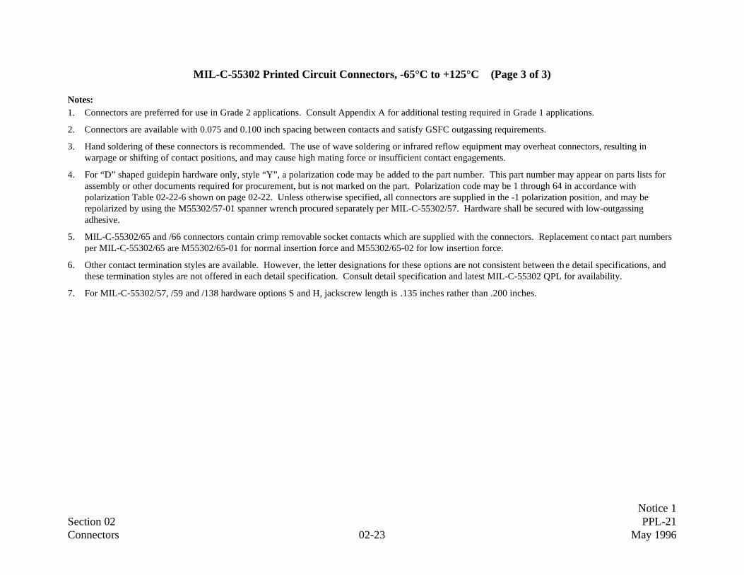
Notice 1Section 02 PPL-21Connectors 02-23 May 1996
MIL-C-55302 Printed Circuit Connectors, -65°C to +125°C (Page 3 of 3)
Notes:1. Connectors are preferred for use in Grade 2 applications. Consult Appendix A for additional testing required in Grade 1 applications.
2. Connectors are available with 0.075 and 0.100 inch spacing between contacts and satisfy GSFC outgassing requirements.
3. Hand soldering of these connectors is recommended. The use of wave soldering or infrared reflow equipment may overheat connectors, resulting inwarpage or shifting of contact positions, and may cause high mating force or insufficient contact engagements.
4. For “D” shaped guidepin hardware only, style “Y”, a polarization code may be added to the part number. This part number may appear on parts lists forassembly or other documents required for procurement, but is not marked on the part. Polarization code may be 1 through 64 in accordance withpolarization Table 02-22-6 shown on page 02-22. Unless otherwise specified, all connectors are supplied in the -1 polarization position, and may berepolarized by using the M55302/57-01 spanner wrench procured separately per MIL-C-55302/57. Hardware shall be secured with low-outgassingadhesive.
5. MIL-C-55302/65 and /66 connectors contain crimp removable socket contacts which are supplied with the connectors. Replacement contact part numbersper MIL-C-55302/65 are M55302/65-01 for normal insertion force and M55302/65-02 for low insertion force.
6. Other contact termination styles are available. However, the letter designations for these options are not consistent between the detail specifications, andthese termination styles are not offered in each detail specification. Consult detail specification and latest MIL-C-55302 QPL for availability.
7. For MIL-C-55302/57, /59 and /138 hardware options S and H, jackscrew length is .135 inches rather than .200 inches.

Notice 1Section 02 PPL-21Connectors 02-24 May 1996
MIL-C-39012 Radio Frequency Connectors, (Notes 1 through 4) (Page 1 of 3)SMA Series Coaxial, 50 Ohms
Part Number Explanation:
M39012 /XX X XXXX
Military Specification Detail Specification - = Field Replaceable (Standard) Dash NumberNumber B = Non-Field Replaceable -3XXX = Corrosion Resistant Steel
Not Preferred (Note 5) Shell, Passivated Finish-4XXX = Beryllium Copper Shell, Gold Finish
Part Numbers(s)Detail Specification Dash Number Configuration Frequency, Max Applicable Cable Type
M39012/55 -3006, -3025, -4006, -4025-3007, -3026, -4007, -4026-3009, -3028, -4009, -4028-3010, -3029, -4010, -4029-3030-3502, -4502
Plug, Pin Contact, CableMount
12.4 GHz M17/93-RG178M17/113-RG316M17/60-RG142M17/111-RG303M17/152-00001M17/128-RG400
M39012/56 -3006, -3025, -4006-3007, -3026, -4007-3009, -3028, -4009, -4028-3010, -3029, -4010-3030-3502, -4502
Plug, Pin Contact, RightAngle, Cable Mount
12.4 GHz M17/93-RG178M17/113-RG316M17/60-RG142M17/111-RG303M17/152-00001M17/128-RG400
M39012/57 -3006, -3025, -4006, -4025-3007, -3026, -4007, -4026-3009, -3028, -4009, -4028-3010, -3029, -4010, -4029-3030-3502, -4502
Receptacle, Socket Contact,Cable Mount
12.4 GHz M17/93-RG178M17/113-RG316M17/60-RG142M17/111-RG303M17/152-00001M17/128-RG400
See notes on page 02-26.

Notice 1Section 02 PPL-21Connectors 02-25 May 1996
MIL-C-39012 Radio Frequency Connectors, (Notes 1 through 4) (Page 2 of 3)SMA Series Coaxial, 50 Ohms
Part Numbers(s)Detail Specification Dash Number Configuration Frequency, Max Applicable Cable Type
M39012/58 -3006, -3025, -4006-3007, -3026, -4007-3009, -3028, -4009-3010, -3029, -4010-3030-3502, -4502
Receptacle, Socket Contact,4 Hole Flange Mount
12.4 GHz M17/93-RG178M17/113-RG316M17/60-RG142M17/111-RG303M17/152-00001M17/128-RG400
M39012/59 -3006, -3025, -4006, -4025-3007, -3026, -4007, -4026-3009, -3028, -4009, -4028-3010, -3029, -4010, -4029-3030-3502, -4502
Receptacle, Socket Contact,D-Hole Jam Nut Mount
12.4 GHz M17/93-RG178M17/113-RG316M17/60-RG142M17/111-RG303M17/152-00001M17/128-RG400
M39012/60 -3001, -4001 (4 Hole)-3002 (2 Hole)
Receptacle, Socket Contact,Solder Cup, 4-Hole or 2-Hole Rear Flange Mount
Not Rated All Flexible CableTypes
M39012/61 -3001, -4001 (Rear Mount)-3002, -4002 (Front Mount)
Receptacle, Socket Contact,Solder Cup, Rear or FrontD-Hole Jam Nut Mount
Not Rated All Flexible CableTypes
M39012/62 -3001, -4001 (Rear Mount)-3002, -4002 (Front Mount)
Receptacle, Socket ContactHermetic Seal, Solder LugRear or Front D-Hole JamNut Mount
Not Rated All Flexible CableTypes
M39012/79 -3009, -3007, -3207-3010, -3008, -3208
Plug, Pin Contact, CableMount, Semirigid
18 GHz M17/133-RG405M17/130-RG402
M39012/80 -3009, -3005, -3007, -3207-3010, -3006, -3008, -3208
Plug, Pin Contact, RightAngle, Semirigid
18 GHz M17/133-RG405M17/130-RG402
M39012/81 -3007, -3011, -3207-3008, -3012, -3208
Receptacle, Socket Contact,Cable Mount, Semirigid
18 GHz M17/133-RG405M17/130-RG402
See notes on page 02-26.

Notice 1Section 02 PPL-21Connectors 02-26 May 1996
MIL-C-39012 Radio Frequency Connectors, (Notes 1 through 4) (Page 3 of 3)SMA Series Coaxial, 50 Ohms
Part Numbers(s)Detail Specification Dash Number Configuration Frequency, Max Applicable Cable Type
M39012/82 -3007, -3011, -3207 (4 Hole)-3013 (2 Hole)-3008, -3012, -3028, (4 Hole)-3014 (2 Hole)
Receptacle, Socket Contact,4 Hole or 2 Hole FlangeMount, Semirigid
18 GHz M17/133-RG405
M17/130-RG402
M39012/83 -3009, -3007, -3011, -3207-3010, -3008, -3012, -3208
Receptacle, Socket Contact,Rear D Hole Jam NutMount, Semirigid
18 GHz M17/133-RG405M17/130-RG402
M39012/93 -3001 (.155L SolderTerminal)-3002 (.125L SolderTerminal)-3003 (.093L SolderTerminal)
Receptacle, Socket Contact,PC Mount 500 MHz to 18 GHz
PC Board Mount
M39012/94 -3001 (.155L SolderTerminal)-3002 (.125L SolderTerminal)-3003 (.093L SolderTerminal)
Receptacle, Socket Contact,PC Mount, Right Angle 500 MHz to 18 GHz
PC Board Mount
Notes:1. Connectors are preferred for use in Grade 2 applications. Consult Appendix A for additional testing required in Grade 1 applications.2. Plug coupling nuts and cable nut mounted connectors may have silicone rubber O-Ring seals which are an outgassing concern. Connectors may require
additional processing for outgassing control. This should include a bake of the connector or replacement of the silicone rubber O-Rings with fluorosiliconeO-Rings which meet outgassing requirements.
3. Temperature range for flexible and semirigid connectors is -65°C to +165°C. Temperature range for PC mounted connectors is -65°C to +105°C.4. The use of safety wire is recommended to secure mated connectors together.5. B designated non-field replaceable connectors are not preferred. Most are inactive for new design.

Notice 1Section 02 PPL-21Connectors 02-27 May 1996
MIL-C-83517 Radio Frequency Connectors (Notes 1 and 2) (Page 1 of 2)Series SMA Transmission Line, 50 Ohms
Part Number Explanation:
M83517 /X XXXXX
Military Specification Detail Specification Dash NumberNumber -31XXX = Corrosion Resistant Steel Shell, Passivated Finish
-32XXX = Corrosion Resistant Steel Shell, Gold Plated-33XXX = Corrosion Resistant Steel Shell, Gold Plated Body and Passivated Coupling Nut
Part Number Flange Mount Configuration Solder Tab Configuration
DetailSpecification
DashNumber
BodyStyle
No. ofMounting Holes Dimensions
Insulator Protrusion FromFlange
M83517/1 -31001, 32001-31002, -32002
Receptacle, SocketContact
2 .005 x .020.005 x .050
31003, -3200331004, 32004
4 005 x .020.005 x .050
M83517/2 -31001, 32001-31002, -32002
Plug, Pin Contact 2 .005 x .020.005 x .050
Flush
31003, -3200331004, 32004
4 005 x .020.005 x .050
M83517/3 -31001, 32001-31002, -32002-31003, -32003-31007, -32007, -33007
Receptacle, SocketContact
2 .050 dia x .012 slot.050 dia x .018 slot.050 dia x .028 slot.050 dia x .025 slot .035 inches
-31004, -32004-31005, -32005, -33005-31006, -32006, -33006
4 .050 dia x .012 slot.050 dia x .018 slot.050 dia x .025 slot
Flush
See notes on page 02-28.

Notice 1Section 02 PPL-21Connectors 02-28 May 1996
MIL-C-83517 Radio Frequency Connectors (Notes 1 and 2) (Page 2 of 2)Series SMA Transmission Line, 50 Ohms
Part Number Flange Mount Configuration Solder Tab Configuration
DetailSpecification
DashNumber
BodyStyle
No. ofMounting Holes Dimensions
Insulator Protrusion FromFlange (inches)
M83517/4 -31001, 32001-31002, -32002
Receptacle, SocketContact
2 .010 dia .057.125
-31003, -32003-31004, -32004-31005, -32005
4
.050
.057
.125
.590M83517/5 -31001, -32001, -33001 Plug, Pin Contact 4 .050 .330
Notes:1. Connectors are preferred for use in Grade 2 applications. Consult Appendix A for additional testing required in Grade 1 applications.2. Temperature range is -65°C to +105°C. Frequency range is 0 to 18GHz.

Notice 1Section 02 PPL-21Connectors 02-29 May 1996
MIL-C-83513 Microminiature Connectors, Pre-Terminated (Notes 1 through 5)Crimp Contacts or Solder Contacts, -55°C to +125°C
Part Number Explanation:
M83513 /0X- X XX N
Military Specification Detail Specification Insert Arrangement Wire Type Shell FinishNumber (Table 02-29-1) (Number of Contacts) (Table 02-29-2) N = Electroless Nickel
A = 9 C = 21 E = 31 G = 51 (Not applicable toB = 15 D = 25 F = 37 H = 100 solder contacts)
Table 02-29-1 Connector Styles Table 02-29-2 Wire Pigtail Termination Types
Notes:1. Connectors are preferred for Grade 2 applications. Consult Appendix A for additional testing
required in Grade 1 applications.2. MIL-C-83513 metal shell receptacle connectors contain a thin silicone rubber interface seal which
may represent an outgassing concern. The seal is pressed in place and may be carefully removedto avoid outgassing. Otherwise, additional processing such as a bake may be required to controloutgassing. All other materials have good outgassing characteristics.
3. All contacts are on .050 inch centers between contacts and are size 24.4. Metal shell connectors are not intermateable with plastic shell connectors.5. Mounting hardware must be supplied separately. For insert arrangements A through G, use MIL-C-83513/5 configurations A or B. For insert
arrangement H, use MIL-C-83513/5 configuration C.6. Detail specification sheets require M22759/33-26 wire to be substituted for M22759/11-22 wire when connectors with finish “N” are used.7. Optional color coding in accordance with MIL-STD-681, as modified by detail specification, may be used.
Part Number Type Termination Shell
M83513/1-XNM83513/2-XN
Plug, Pin ContactsReceptacle, Socket Contacts
Soldercup Aluminum,Electroless
M83513/3-XXXNM83513/4-XXXN
Plug, Pin ContactsReceptacle, Socket Contacts
Wire Pigtails Nickel Plated
M83513/6-XM83513/7-X
Plug, Pin ContactsReceptacle, Socket Contacts
Soldercup All Plastic
M83513/8-XXM83513/9-XXX
Plug, Pin ContactsReceptacle, Socket Contacts
Wire Pigtails
Code Wire Length
0102
M22759/33-26-9 (Note 6) 18”L36”L
0304
M22759/33-26-X (Notes 6, 7) 18”L36”L
0506
QQ-W-343, Solid 25 AWG, Gold Plated
.5”L1.0”L
0708
QQ-W-343, Solid 25 AWG, Tin Plated
.5”L1.0”L
0910
M22759/33-26-9 18”L36”L
1112
M22759/33-26-X 18”L36”L
13141516
M22759/11-26-9M22759/11-26-X (Note 7)M22759/33-26-9M22759/33-26-X (Note 7)
72”L
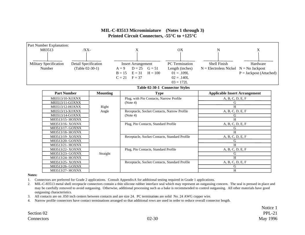
Notice 1Section 02 PPL-21Connectors 02-30 May 1996
MIL-C-83513 Microminiature (Notes 1 through 3)Printed Circuit Connectors, -55°C to +125°C
Part Number Explanation:M83513 /XX- X OX N X
Military Specification Detail Specification Insert Arrangement PC Termination Shell Finish HardwareNumber (Table 02-30-1) A = 9 D = 25 G = 51 Length (inches) N = Electroless Nickel N = No Jackpost
B = 15 E = 31 H = 100 01 = .109L P = Jackpost (Attached)C = 21 F = 37 02 = .140L
03 = 172LTable 02-30-1 Connector Styles
Part Number Mounting Type Applicable Insert ArrangementM83513/10-XOXNXM83513/11-GOXNXM83513/12-HOXNX Right
Plug, with Pin Contacts, Narrow Profile(Note 4)
A, B, C, D, E, FGH
M83513/13-XOXNXM83513/14-GOXNXM83513/15- HOXNX
Angle Receptacle, Socket Contacts, Narrow Profile(Note 4)
A, B, C, D, E, FGH
M83513/16- XOXNXM83513/17- GOXNXM83513/18- HOXNX
Plug, Pin Contacts, Standard Profile A, B, C, D, E, FGH
M83513/19- XOXNXM83513/20- GOXNXM83513/21- HOXNX
Receptacle, Socket Contacts, Standard Profile A, B, C, D, E, FGH
M83513/22- XOXNXM83513/23- GOXNXM83513/24- HOXNX
StraightPlug, Pin Contacts, Standard Profile A, B, C, D, E, F
GH
M83513/25- XOXNXM83513/26- GOXNXM83513/27- HOXNX
Receptacle, Socket Contacts, Standard Profile A, B, C, D, E, FGH
Notes:1. Connectors are preferred for Grade 2 applications. Consult Appendix A for additional testing required in Grade 1 applications.2. MIL-C-83513 metal shell receptacle connectors contain a thin silicone rubber interface seal which may represent an outgassing concern. The seal is pressed in place and
may be carefully removed to avoid outgassing. Otherwise, additional processing such as a bake is recommended to control outgassing. All other materials have goodoutgassing characteristics.
3. All contacts are on .050 inch centers between contacts and are size 24. PC terminations are solid No. 24 AWG copper wire.4. Narrow profile connectors have contact terminations arranged so that additional rows are used in order to reduce overall connector length.

Notice 1Section 02 PPL-21Connectors 02-31 May 1996
GSFC S-311-P-718 Satellite Interface Connectors (Notes 1 and 2) (Page 1 of 5)Receptacle, Rectangular, Polarized Shell, EMI Shielded, Crimp Removable Pin Contacts
Part Number Explanation:700-42/ X -X -X
GSFC Prefix Detail Specification No. Insert Arrangement Contact TypeP = PinS = Socket
GSFC GSFC Shell Pin Contacts, Crimp (Note 3) GSFC Contact For Use WithPart Number Specification Size Qty. Size Part Number Wire Size (AWG)
GPP17 88 8 GPP18 12
GPP19 10700-42/3-1-P 1 58 16 GPP20 16, 18, 20
GPP21 22, 24, 266 RG393 (Note 4) GCP14 M17/127-RG3936 RG142 (Note 4) GCP15 M17/60-RG142
GPP17 826 8 GPP18 12
700-42/3-2-P S-311-P-718/3 1 GPP19 1086 16 GPP20 16, 18, 20
GPP21 22, 24, 262 RG142 (Note 4) GCP15 M17/60-RG142
700-42/3-3-P 1 244 16 GPP20 16, 18, 20GPP21 22, 24, 26GPP17 8
20 8 GPP18 12700-42/3-4-P 1 GPP19 10
144 16 GPP20 16, 18, 20GPP21 22, 24, 26
See notes on page 02-35.

Notice 1Section 02 PPL-21Connectors 02-32 May 1996
GSFC S-311-P-718 Satellite Interface Connectors (Notes 1 and 2) (Page 2 of 5)Receptacle, Rectangular, Polarized Shell, EMI Shielded, Crimp Removable Pin Contacts
GSFC GSFC Shell Pin Contacts, Crimp (Note 3) GSFC Contact For Use WithPart Number Specification Size Qty. Size Part Number Wire Size (AWG)
10 16 GPP22 16, 18, 20GPP23 22, 24, 26
700-42/5-1-P 2 4 20 GPP24 20, 22, 2488 22 GPP25 22, 24, 26
RG122 (Notes 4, 5) GCP29 M17/54-RG122(Note 5)
16 16 GCP22 16, 18, 20GCP23 22, 24, 26
S-311-P-718/5 52 20 GPP24 20, 22, 24700-42/5-2-P 2 RG142 (Note 4) GCP28 M17/60-RG142
2 Triaxial GTP26 Raychem 9530D5117(Note 6) Databus GDP27 Champion 51-05091
8 16 GPP22 16, 18, 20700-42/6-1-P 3 GCP23 22, 24, 26
12 20 GPP24 20, 22, 24S-311-P-718/6 20 22 GPP25 22, 24, 26
700-42/6-2-P 3 28 20 GPP24 20, 22, 241 RG393 (Note 4) GCP14 M17/127-RG393
See notes on page 02-35.

Notice 1Section 02 PPL-21Connectors 02-33 May 1996
GSFC S-311-P-718 Satellite Interface Connectors (Notes 1 and 2) (Page 3 of 5)Plug, Rectangular, Polarized Shell, EMI Shielded, Crimp Removable Socket Contacts
GSFC GSFC Shell Pin Contacts, Crimp (Note 3) GSFC Contact For Use WithPart Number Specification Size Qty. Size Part Number Wire Size (AWG)
GPS10 88 8 GPS11 12
GPS16 10700-42/3-1-S 1 58 16 GPS20 16, 18, 20
GPS21 22, 24, 266 RG393 (Note 4) GCC14 M17/127-RG393
RG142 (Note 4) GCS15 M17/60-RG142GPS10 8
26 8 GPS11 12700-42/3-2-S S-311-P-718/3 GPS16 10
1 86 16 GPS20 16, 18, 20GPS21 22, 24, 26
2 RG142 (Note 4) GCS15 M17/60-RG142700-42/3-5-S 1 244 16 GPS20 16, 18, 20
GPS21 22, 24, 26GPS10 8
1 20 8 GPS11 12700-42/3-4-S GPS16 10
144 16 GPS20 16, 18, 20GPS21 22, 24, 26
See notes on page 02-35.

Notice 1Section 02 PPL-21Connectors 02-34 May 1996
GSFC S-311-P-718 Satellite Interface Connectors (Notes 1 and 2) (Page 4 of 5)Plug, Rectangular, Polarized Shell, EMI Shielded, Crimp Removable Socket Contacts
GSFC GSFC Shell Pin Contacts, Crimp (Note 3) GSFC Contact For Use WithPart Number Specification Size Qty. Size Part Number Wire Size (AWG)
10 16 GPS22 16, 18, 20GPS23 22, 24, 26
700-42/5-1-S 2 4 20 GPS24 20, 22, 2488 22 GPS25 22, 24, 26
S-311-P-718/51 RG122 (Notes 4, 5) GCS29 M17/54-RG122
(Note 5)16 16 GPS22 16, 18, 20
GPS23 22, 24, 2652 20 GPS24 20, 22, 24
700-42/5-2-S 2 RG142 (Note 4) GCS28 M17/60-RG1422 Triaxial GTS26 Raychem 9530D5117
(Note 6) Databus GDS27 Champlain 51-050918 16 GPS22 16, 18, 20
GPS23 22, 24, 26700-42/6-1-S S-311-P-718/6 3 12 20 GPS24 20, 22, 24
20 22 GPS25 22, 24, 26
700-42/6-2-S 3 28 20 GPS24 20, 22, 24
1 RG393 (Note 4) GCS14 M17/127-RG393
See notes on page 02-35.

Notice 1Section 02 PPL-21Connectors 02-35 May 1996
GSFC S-311-P-718 Satellite Interface Connectors (Page 5 of 5)
Notes:1. Connectors are for Grade 1 and Grade 2 applications. Connectors are intended to be used for power and signal interfaces between satellite main structure
and subsystem modules. Temperature range for these connectors is -65°C to +125°C.
2. Strain relief backshell kits shall be procured to GSFC Specification S-311-P-718/4. Part numbers are as follows:
Part NumberAccommodating GSFC
Connector P/N Shell Size Description
G1RG1SG2RG3R
700-42/3-X-X700-42/3-X-X700-42/5-X-X700-42/6-X-X
1123
Kit, EMI Backshell with Clamp, Round Entry HoleKit, EMI Backshell with Clamp, Square Entry HoleKit, EMI Backshell with Clamp, Round Entry HoleKit, EMI Backshell with Clamp, Round Entry Hole
3. Connectors are supplied without contacts. Contacts shall be procured to GSFC Specification S-311-P-718/2.
Example of Contact Part Number:G X X XX
GSFC Prefix Contact Description Contact Type Two DigitP = Power T = Triaxial P = Pin DesignatorC = Coaxial D = Databus S = Socket from
S-311-P-718/2
4. Designates coaxial contact for use with coaxial cable from MIL-C-17. Refer to S-311-P-718/2 for coaxial contact installation details.
5. RG122 is for reference only and is not space compatible.
6. Coaxial, triaxial or databus contacts may be used with this connector.

Notice 1Section 02 PPL-21Connectors 02-36 May 1996
THIS PAGE INTENTIONALLY LEFT BLANK
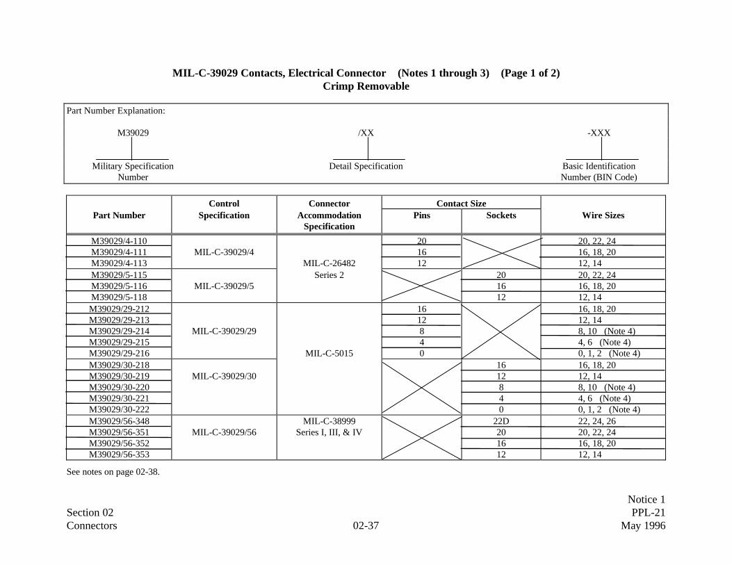
Notice 1Section 02 PPL-21Connectors 02-37 May 1996
MIL-C-39029 Contacts, Electrical Connector (Notes 1 through 3) (Page 1 of 2)Crimp Removable
Part Number Explanation:
M39029 /XX -XXX
Military Specification Detail Specification Basic IdentificationNumber Number (BIN Code)
Control Connector Contact SizePart Number Specification Accommodation
SpecificationPins Sockets Wire Sizes
M39029/4-110M39029/4-111M39029/4-113
MIL-C-39029/4MIL-C-26482
201612
20, 22, 2416, 18, 2012, 14
M39029/5-115M39029/5-116M39029/5-118
MIL-C-39029/5Series 2 20
1612
20, 22, 2416, 18, 2012, 14
M39029/29-212M39029/29-213M39029/29-214M39029/29-215M39029/29-216
MIL-C-39029/29
MIL-C-5015
1612840
16, 18, 2012, 148, 10 (Note 4)4, 6 (Note 4)0, 1, 2 (Note 4)
M39029/30-218M39029/30-219M39029/30-220M39029/30-221M39029/30-222
MIL-C-39029/301612840
16, 18, 2012, 148, 10 (Note 4)4, 6 (Note 4)0, 1, 2 (Note 4)
M39029/56-348M39029/56-351M39029/56-352M39029/56-353
MIL-C-39029/56MIL-C-38999
Series I, III, & IV22D201612
22, 24, 2620, 22, 2416, 18, 2012, 14
See notes on page 02-38.

Notice 1Section 02 PPL-21Connectors 02-38 May 1996
MIL-C-39029 Contacts, Electrical Connector (Notes 1 through 3) (Page 2 of 2)Crimp Removable
Control Connector Contact SizePart Number Specification Accommodation
SpecificationPins Sockets Wire Sizes
M39029/57-354M39029/57-357M39029/57-358M39029/57-359
MIL-C-39029/57MIL-C-38999
Series II22D201612
22, 24, 2620, 22, 2416, 18, 2012, 14
M39029/58-360M39029/58-363M39029/58-364M39029/58-365
MIL-C-39029/58MIL-C-38999
Series I, II, III, & IV22D201612
22, 24, 2620, 22, 2416, 18, 2012, 14
M39029/63-368M39029/64-369
MIL-C-39029/63MIL-C-39029/64
MIL-C-24308 —20
20—
20, 22, 2420, 22, 24
M39029/57-354M39029/58-360
MIL-C-39029/57MIL-C-39029/58
—22D
22D—
22, 24, 2622, 24, 26
Notes:1. Contacts are preferred for Grade 2 applications. Consult Appendix A for additional screening required in Grade 1 applications.2. Identification color bands on these contacts may be an outgassing concern. Additional processing may be required for outgassing control.3. Contacts have gold finish per MIL-C-45204, Type II, Grade C, Class 1 (50 microinches, minimum) applied to the contact engagement area. The entire
contact is finished in Gold.4. Electrically conductive bushings as provided in MS3348 should be used when crimping wire sizes 10, 6, and 2 in contact sizes 8, 4, and 0 respectively.
Example of P/N: MS3348-8-10 where 8 is contact wire barrel size and 10 is wire size.

Notice 1Section 02 PPL-21Connectors 02-39 May 1996
MIL-C-85049 Connector Accessories, Electrical (Notes 1 through 3) (Page 1 of 2)
Part Number Explanation: (Refer to detail specification for shell sizes):M85049 /10 - XX N
/15 S XX N/36 XX N XX X/76 - XX N XX
Military Detail S = Self Connector Nickel Clamp BackshellSpecification Specification Locking Type Shell Finish Size Length
Number Only (Not SizeAvailable for
all Types)
Notes:1. Refer to page 02-40 for a table of preferred backshell connector accessories.2. Preferred for Grades 1 and 2. All backshells in this section are nickel plated and are rated -65°C to +200°C. Consult latest Qualified Products List (QPL)
for availability.3. The use of safety wire is recommended to secure backshells which are not self-locking.4. When procuring backshell accessories for use with MIL-C-38999 Series I connectors, complete the part number by specifying the equivalent Series II shell
size. For example, when ordering Series I shell size 9, specify Series II shell size 8. For shell size 11, specify shell size 10, etc.5. Environmentally sealed backshells contain a silicone rubber grommet and O ring which represents an outgassing concern. Additional processing for
outgassing control, such as a bake, is recommended.6. Backshell is equipped with an arm which extends from the rear of the backshell body. Strain relief is accomplished through the use of Tefzel tie wraps,
lacing twine, or lacing tape, which is tied to the arm, and must be provided separately.7. Backshell requires M85049/26-2-XX crimp ferrule ring to terminate shield to backshell. Ring is supplied with M85049/26-3, but must be provided
separately for M85049/20 and M85049/33-2 backshells. Backshell M85049/26-1 may be used in lieu of M85049/26-3, but crimp ferrule ring M85049/26-2 must be provided separately. Ferrule requires Thomas & Betts Crimp Tool No. 13640 or equivalent and appropriate size die.
8. Ring type backshells have a chamfered edge which, when installed to the rear of the connector, compresses the connector’s silicone rubber grommet sealaround the exiting wires to provide limited seal and strain relief. Intended for unit mounted connector receptacles only.
9. Backshell is used to terminate the shields of individually shielded wires, or to terminate the shields of several MIL-C-27500 type shielded cables.

Section 02 PPL-21Connectors 02-40 March 1995
MIL-C-85049 Connector Accessories, Electrical (Notes 1 through 3) (Page 2 of 2)
Applicable Connector ProcurementSpecification Backshell Description Strain Relief Type Configuration
5015 26482 38999 Series
Part Number NotesCrimp Series 2 I & II
(Note 4)III &
IV SealedSelf
LockingShield
Termination ClampTie
Wrap Ring Straight 45° 90°M85049/6-XXNM85049/7-XXNM85049/8-XXNM85049/9-XXNM85049/10-XXN
(Note 5)(Note 5)(Note 5)(Note 5)(Note 5)
XXXXX
XXXXX
XXXXX
X
X
X
XXXXX X
XX
XX
M85049/11-XXNM85049/15SXXNM85049/16SXXNM85049/17XXNXXXM85049/18XXNXXX
(Note 5)(Note 6)(Note 6)(Note 5)(Note 5)
X X
X
XX
X
X
XX
XX
XX
X
XX
XX
X
XX
XX
M85049/19XXNXXXM85049/20-XXNM85049/23-XXNM85049/24-XXNM85049/25-XXN
(Note 7)XXX
XXX
XX
XX (Crimp Ring)
XXX
XXX
XX
X
XX
M85049/26-3-XXNM85049/27SXXNM85049/30-XXNM85049/31SXXN
(Note 7)(Note 8)(Note 9)(Note 8)
X
X
X
X
X (Series II Only)
XX
X
X (Crimp Ring)
X (Daisy Chain)
X
X
XXXX
M85049/33-2-XXNM85049/36XXNXXXM85049/38SXXNM85049/39SXXNM85049/43-XXN
(Note 7)
X X
XX
XX
XX
X (Crimp Ring)
X XXXX
XXX
XX
M85049/47SNXXM85049/49-2SXXNM85049/51SXXNM85049/52SXXNM85049/56-XXN (Note 6)
XX
XX
XX
X
XXXX
XXXX
X
X
XX
X
X
M85049/57SXXNM85049/63SXXNM85049/76-XXNXXM85049/77-XXNXXM85049/78-XXNXXM85049/79-XXNXX
(Note 6)(Note 6)(Note 5)(Note 5)(Note 5)(Note 5)
XXXX
XX
XXXX
XX
XXXX
XXXX
XX
X
XX
XX
XSee notes on page 02-39.

Section 03 PPL-21Filters 03-1 March 1995
Summary of Preferred Filters
ControlSpecification
Description
Minimum InsertionLoss Range
-55°C to +125°C(dB)
Frequency Range-55°C to +125°C
(Hz)Grade 1 Grade 2 Refer to
Page No.
MIL-F-28861 (Note 1) RF & EMIsuppression
3 - 80 15K - 1.0G Class S(Note 2)
Class B 03-2
Notes:1. For stud-mounted filters, do not exceed the rated torque specification.2. There are currently no Class S filters available.

Section 03 PPL-21Filters 03-2 March 1995
MIL-F-28861 Filters, Radio Frequency/Electromagnetic Interference Suppression
Part Number Explanation:M28861 /X -XXX X X
Military Specification Detail Specification Dash Number Case Finish Product Assurance LevelNumber Number uniquely defines the T = Tin-plated/tin-lead plated B = Class B
the circuits, rated voltage S = Silver-plated S = Class Sand current, capacitance, G = Gold plated (Class S)
and insertion loss.
Part Number Style Rated VoltageRated
CurrentOperating
TemperatureMinimum
Capacitance Circuit FrequencyMinimum
Insertion Loss Grade(Note 1) (Note 2) (Vdc) (Vac) (Amperes) Range Range (µµF) Type Range (Hz) (dB) (Note 3) 1 2
M28861/1-XXXXX FS10, 11 50-200 125 (0 to400 Hz)(Note 4)
15 0.15 - 0.7 C or L2 30K - 1.0G 7-40
M28861/2-XXXXX FS20 100 - 0.25 - 5.0 -55°Cto
+125°
0.45 - 0.9 L1 L2 or P1 100K - 1.0G 12-80 Class S(Note 5)
Class B
M28861/4-XXXXX FS40 70 - 0.1 - 5.0 0.70 - 1.4 L1 L2 or P1 15K - 1.0G 3-80
M28861/5-XXXXX FS50 200 125 (0 to400 Hz)
0.25 - 50 0.15 - 0.3 L1 L2 or P1 100K - 1.0G 3-80
Notes:1. Parts covered by these specifications contain internal solder connections that may reflow during installation. Special care must be exercised when
soldering to prevent internal solder reflow.2. Style is denoted by FS followed by a two digit number, which indicates the voltage rating, envelope size and configuration.3. Minimum insertion loss values are given in Table 1 of each detail specification (slash sheet) for frequency increments within the specified range over the
temperature range of -55°C to +125°C.4. Only dash numbers 009, 010, 019, and 020 have AC voltage ratings.5. There are currently no Class S filters available.

Section 04 PPL-21Fuses 04-1 March 1995
Summary of Preferred Fuses (Note 1)
Style andCharacteristic
(Note 2)Description Specification
Current Range(Note 3)
(Amperes)
Voltage Rating(Note 4)(Volts)
Grades Refer ToPage No.
FM08ASubminiature, High
Performance, Cartridge,Instrument Type
MIL-F-23419/8 1/8 - 1015
12532
1 Page 04-2
FM04ASubminiature,
Nonindicating, Cartridge,Instrument Type
MIL-F-23419/4 1/8 - 15 125 2 Page 04-2
Notes:1. All electrical ratings are both direct current (dc) and alternating current (ac) up to 400 hertz.2. Characteristic “A” denotes the fuse has a normal relative overload interrupt time, commonly referred to as a “normal blow” fuse. This fuse contains a
single element with no intentional time delay designed into the element.3. Current rating is defined in MIL-F-23419 as the amount of current a fuse will carry indefinitely without interruption. This should not be construed to
mean that these fuses will operate for an infinite time at rated load current. For all amperages, continuous operation at 100% of load will degrade the fuseand cause it to open after a finite period of time. For example, one of the FM08 manufacturers advertises that these fuses, when operated at 100% of load,have a 4 hours (minimum) opening time.
4. The voltage rating is the maximum direct current (dc) or alternating current (ac) voltage for which a fuse is designed.
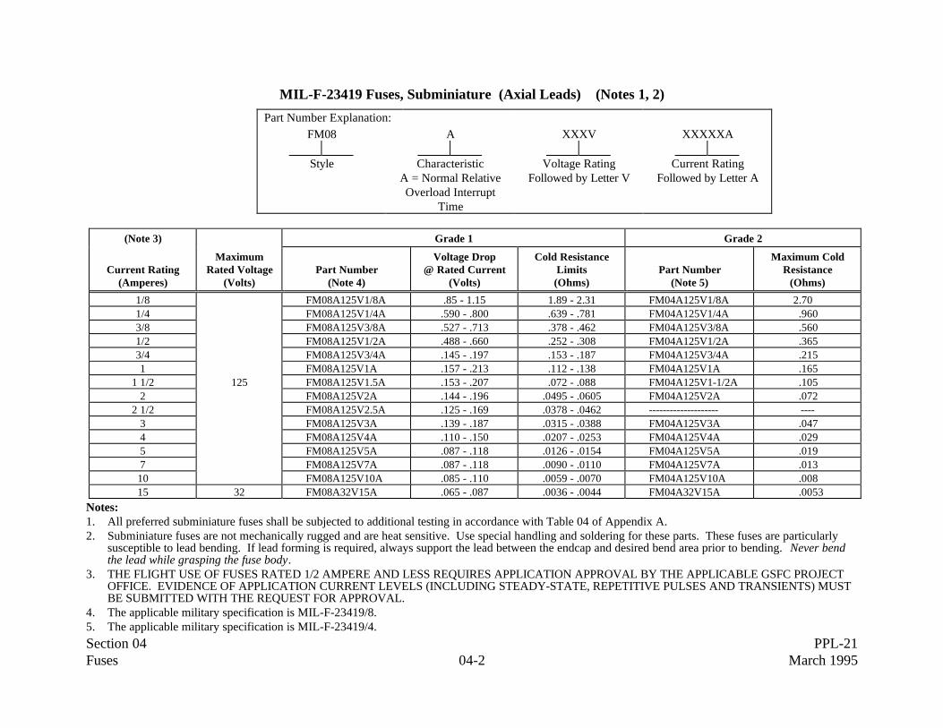
Section 04 PPL-21Fuses 04-2 March 1995
MIL-F-23419 Fuses, Subminiature (Axial Leads) (Notes 1, 2)
Part Number Explanation:FM08 A XXXV XXXXXA
Style CharacteristicA = Normal RelativeOverload Interrupt
Time
Voltage RatingFollowed by Letter V
Current RatingFollowed by Letter A
(Note 3) Grade 1 Grade 2
Current Rating(Amperes)
MaximumRated Voltage
(Volts)Part Number
(Note 4)
Voltage Drop@ Rated Current
(Volts)
Cold ResistanceLimits(Ohms)
Part Number(Note 5)
Maximum ColdResistance
(Ohms)
1/8 FM08A125V1/8A .85 - 1.15 1.89 - 2.31 FM04A125V1/8A 2.701/4 FM08A125V1/4A .590 - .800 .639 - .781 FM04A125V1/4A .9603/8 FM08A125V3/8A .527 - .713 .378 - .462 FM04A125V3/8A .5601/2 FM08A125V1/2A .488 - .660 .252 - .308 FM04A125V1/2A .3653/4 FM08A125V3/4A .145 - .197 .153 - .187 FM04A125V3/4A .2151 FM08A125V1A .157 - .213 .112 - .138 FM04A125V1A .165
1 1/2 125 FM08A125V1.5A .153 - .207 .072 - .088 FM04A125V1-1/2A .1052 FM08A125V2A .144 - .196 .0495 - .0605 FM04A125V2A .072
2 1/2 FM08A125V2.5A .125 - .169 .0378 - .0462 -------------------- ----3 FM08A125V3A .139 - .187 .0315 - .0388 FM04A125V3A .0474 FM08A125V4A .110 - .150 .0207 - .0253 FM04A125V4A .0295 FM08A125V5A .087 - .118 .0126 - .0154 FM04A125V5A .0197 FM08A125V7A .087 - .118 .0090 - .0110 FM04A125V7A .01310 FM08A125V10A .085 - .110 .0059 - .0070 FM04A125V10A .00815 32 FM08A32V15A .065 - .087 .0036 - .0044 FM04A32V15A .0053
Notes:1. All preferred subminiature fuses shall be subjected to additional testing in accordance with Table 04 of Appendix A.2. Subminiature fuses are not mechanically rugged and are heat sensitive. Use special handling and soldering for these parts. These fuses are particularly
susceptible to lead bending. If lead forming is required, always support the lead between the endcap and desired bend area prior to bending. Never bendthe lead while grasping the fuse body.
3. THE FLIGHT USE OF FUSES RATED 1/2 AMPERE AND LESS REQUIRES APPLICATION APPROVAL BY THE APPLICABLE GSFC PROJECTOFFICE. EVIDENCE OF APPLICATION CURRENT LEVELS (INCLUDING STEADY-STATE, REPETITIVE PULSES AND TRANSIENTS) MUSTBE SUBMITTED WITH THE REQUEST FOR APPROVAL.
4. The applicable military specification is MIL-F-23419/8.5. The applicable military specification is MIL-F-23419/4.

Notice 1Section 05 PPL-21Coils/Inductors 05-1 May 1996
Summary of Preferred Coils/Inductors
Inductance Range Q FRL Refer toSpecification Description Min Max (min) Range Grade 1 Grade 2 Page No.
MIL-C-39010 Fixed, molded, radio frequency 0.1 µH 100.0 mH 75 - 18 S (Note 1) R, P 05-2
MIL-C-83446 Chip, radio frequency, fixed or variable 0.01 µH 1,000 µH 75 - 19 Note 2 05-3
Notes:1. There are currently no failure rate level S parts available. Failure rate level R or P parts may be used in Grade 1 applications if they meet the Class S
requirements of MIL-STD-981.2. Failure rate level is not applicable. These inductors may be used in Grade 2 applications. They may be used in Grade 1 applications if they meet the Class S
requirements of MIL-STD-981 (Groups A and B testing).
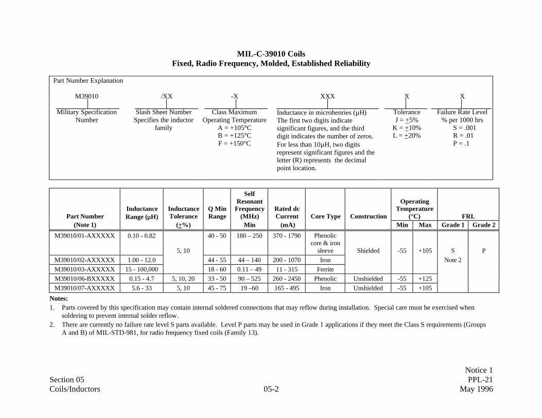
Notice 1Section 05 PPL-21Coils/Inductors 05-2 May 1996
MIL-C-39010 CoilsFixed, Radio Frequency, Molded, Established Reliability
Part Number Explanations
M39010 /XX -X XXX X X
Military SpecificationNumber
Slash Sheet NumberSpecifies the inductor
family
Class MaximumOperating Temperature
A = +105°CB = +125°CF = +150°C
Inductance in microhenries (µH)The first two digits indicatesignificant figures, and the thirddigit indicates the number of zeros.For less than 10µH, two digitsrepresent significant figures and theletter (R) represents the decimalpoint location.
ToleranceJ = +5%
K = +10%L = +20%
Failure Rate Level% per 1000 hrs
S = .001R = .01P = .1
Part NumberInductanceRange (µµH)
InductanceTolerance
Q MinRange
SelfResonant
Frequency(MHz)
Rated dcCurrent Core Type Construction
OperatingTemperature
(°C) FRL(Note 1) (+%) Min (mA) Min Max Grade 1 Grade 2
M39010/01-AXXXXX 0.10 - 0.82
5, 10
40 - 50 180 – 250 370 - 1790 Phenoliccore & iron
sleeve Shielded -55 +105 S PM39010/02-AXXXXX 1.00 - 12.0 44 - 55 44 – 140 200 - 1070 Iron Note 2M39010/03-AXXXXX 15 - 100,000 18 - 60 0.11 – 49 11 - 315 FerriteM39010/06-BXXXXX 0.15 - 4.7 5, 10, 20 33 - 50 90 – 525 260 - 2450 Phenolic Unshielded -55 +125M39010/07-AXXXXX 5.6 - 33 5, 10 45 - 75 19 –60 165 - 495 Iron Unshielded -55 +105
Notes:1. Parts covered by this specification may contain internal soldered connections that may reflow during installation. Special care must be exercised when
soldering to prevent internal solder reflow.2. There are currently no failure rate level S parts available. Level P parts may be used in Grade 1 applications if they meet the Class S requirements (Groups
A and B) of MIL-STD-981, for radio frequency fixed coils (Family 13).

Notice 1Section 05 PPL-21Coils/Inductors 05-3 May 1996
MIL-C-83446, CoilsChip, Fixed or Variable, Radio Frequency
Part Number Explanations
M83446 /XX -XX X
Military SpecificationNumber
Slash Sheet NumberSpecifies the inductor family
Sequential Dash NumberSpecifies individual
inductor characteristics
Termination FinishA = Gold over nickelB = Tin-lead over nickelC = Tin platedD = Platinum-goldE = Palladium-silverF = Tin-lead
Part Number InductanceInductanceTolerance Q Min
SelfResonant
Frequency(MHz)
Rated dcCurrent Configuration Construction
OperatingTemperature
(°C) GradeRange (µµH) (+%) Range Min (mA) Min Max 1 2
M83446/04-XXX 0.010 - 27.0 10, 20 22 - 60 22.0 - 2700 120 - 1270 Fixed
M83446/05-XXX 0.01 - 10.0 10 42 - 60 33.0 - 2000 87 - 750 FixedM83446/07-XXX 0.016 - 76.1 __ 19 - 55 5.0 - 1200 22 - 750 Variable Unshielded -55 +125 (Note 1)
M83446/09-XXX 0.015 - 150 __ 22 - 55 3.0 - 1200 22 - 750 Variable
M83446/10-XXX 0.01 - 1000.0 10 30 - 75 1.7 - 2000 25 - 1000 Fixed
Notes:1. These inductors may be used in Grade 1 applications only if they meet the Class S requirements of MIL-STD-981. They may be used “as is” for Grade 2
applications.

Notice 1Section 05 PPL-21Coils/Inductors 05-4 May 1996
THIS PAGE INTENTIONALLY LEFT BLANK
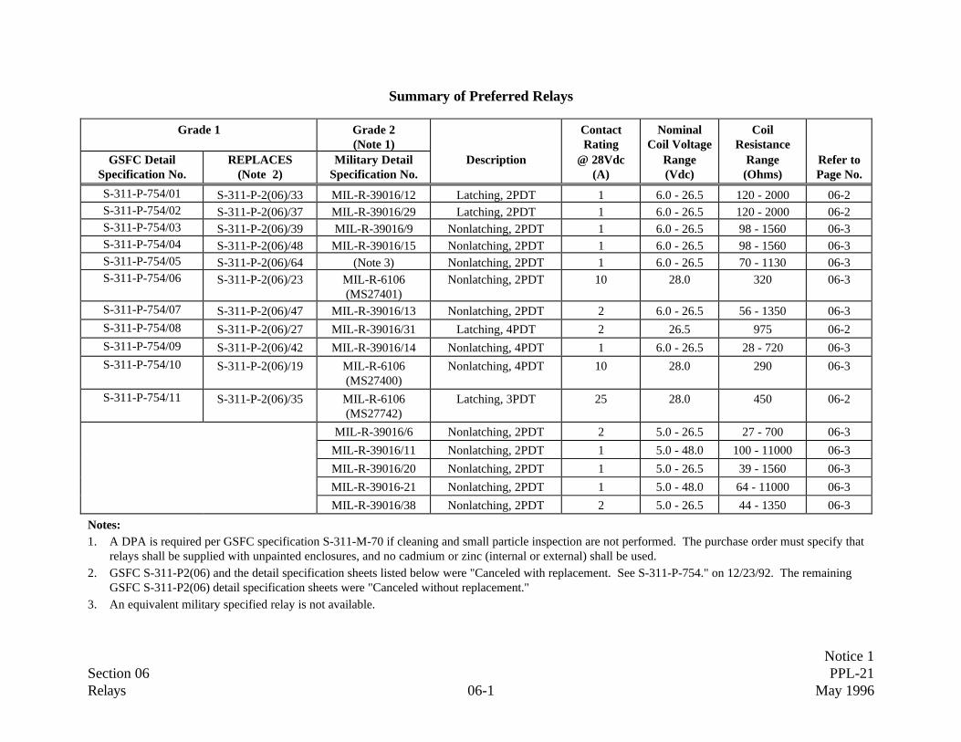
Notice 1Section 06 PPL-21Relays 06-1 May 1996
Summary of Preferred Relays
Grade 1 Grade 2(Note 1)
ContactRating
NominalCoil Voltage
CoilResistance
GSFC DetailSpecification No.
REPLACES(Note 2)
Military DetailSpecification No.
Description @ 28Vdc(A)
Range(Vdc)
Range(Ohms)
Refer toPage No.
S-311-P-754/01 S-311-P-2(06)/33 MIL-R-39016/12 Latching, 2PDT 1 6.0 - 26.5 120 - 2000 06-2S-311-P-754/02 S-311-P-2(06)/37 MIL-R-39016/29 Latching, 2PDT 1 6.0 - 26.5 120 - 2000 06-2S-311-P-754/03 S-311-P-2(06)/39 MIL-R-39016/9 Nonlatching, 2PDT 1 6.0 - 26.5 98 - 1560 06-3S-311-P-754/04 S-311-P-2(06)/48 MIL-R-39016/15 Nonlatching, 2PDT 1 6.0 - 26.5 98 - 1560 06-3S-311-P-754/05 S-311-P-2(06)/64 (Note 3) Nonlatching, 2PDT 1 6.0 - 26.5 70 - 1130 06-3S-311-P-754/06 S-311-P-2(06)/23 MIL-R-6106
(MS27401)Nonlatching, 2PDT 10 28.0 320 06-3
S-311-P-754/07 S-311-P-2(06)/47 MIL-R-39016/13 Nonlatching, 2PDT 2 6.0 - 26.5 56 - 1350 06-3S-311-P-754/08 S-311-P-2(06)/27 MIL-R-39016/31 Latching, 4PDT 2 26.5 975 06-2S-311-P-754/09 S-311-P-2(06)/42 MIL-R-39016/14 Nonlatching, 4PDT 1 6.0 - 26.5 28 - 720 06-3S-311-P-754/10 S-311-P-2(06)/19 MIL-R-6106
(MS27400)Nonlatching, 4PDT 10 28.0 290 06-3
S-311-P-754/11 S-311-P-2(06)/35 MIL-R-6106(MS27742)
Latching, 3PDT 25 28.0 450 06-2
MIL-R-39016/6 Nonlatching, 2PDT 2 5.0 - 26.5 27 - 700 06-3MIL-R-39016/11 Nonlatching, 2PDT 1 5.0 - 48.0 100 - 11000 06-3MIL-R-39016/20 Nonlatching, 2PDT 1 5.0 - 26.5 39 - 1560 06-3MIL-R-39016-21 Nonlatching, 2PDT 1 5.0 - 48.0 64 - 11000 06-3MIL-R-39016/38 Nonlatching, 2PDT 2 5.0 - 26.5 44 - 1350 06-3
Notes:1. A DPA is required per GSFC specification S-311-M-70 if cleaning and small particle inspection are not performed. The purchase order must specify that
relays shall be supplied with unpainted enclosures, and no cadmium or zinc (internal or external) shall be used.2. GSFC S-311-P2(06) and the detail specification sheets listed below were "Canceled with replacement. See S-311-P-754." on 12/23/92. The remaining
GSFC S-311-P2(06) detail specification sheets were "Canceled without replacement."3. An equivalent military specified relay is not available.

Notice 1Section 06 PPL-21Relays 06-2 May 1996
Relays, Latching
Grade 1 Grade 2 Electrical Data (Note 3) Mechanical Data
GSFCSpecificationS-311-P-754
REPLACESGSFC
SpecificationS-311-P2(06)
Military PartNumber
ContactRating
at 28 Vdc(Note 2)
Coil Voltage
NominalCoil
ResistanceContact
FormPackage
TypeTerminal
Type
(Amps)Nominal
(Vdc)Pick-up
(Max Vdc) (Ohms) (Note 4)G311P754/01-001G311P754/01-002G311P754/01-003G311P754/01-004G311P754/01-005
(Note 1)
P2/33-05P2/33-04P2/33-03P2/33-02P2/33-01
M39016/12-056MM39016/12-057MM39016/12-058MM39016/12-059MM39016/12-060M
1
6.09.0
12.018.026.5
4.56.89.0
13.518.0
120280500
11302000
2 Form C(2PDT)
TO-5Can
WireLeads
G311P754/02-001G311P754/02-002G311P754/02-003G311P754/02-004G311P754/02-005
(Note 1)
P2/37-05P2/37-04P2/37-03P2/37-02P2/37-01
M39016/29-056MM39016/29-057MM39016/29-058MM39016/29-059MM39016/29-060M
1
6.09.0
12.018.026.5
4.56.89.0
13.518.0
120280500
11302000
2 Form C(2PDT)
TO-5Can
WireLeads
G311P754/08-003 P-2(06)/27-01 M39016/31-003M 2.0(Note 5)
26.5 13.5 975 4 Form C(4PDT)
LowProfile
Pins
G311P754/11-001 P-2(06)/35-01 MS27742-125.0 28.0 18.0 ---
3 Form C(3PDT)
One InchCube
SolderHook
G311P754/11-002 P-2(06)/35-02 MS27742-2 Plug-inNotes:1. The GSFC relay part numbers specify a 1.500 inch minimum lead length, whereas the corresponding MIL relay part numbers specify a 0.500 inch
minimum lead length.2. Contact ratings for other types of loads (inductive, capacitive, lamp, motor, etc.) can be obtained from the detail specifications.3. Electrical data are for +25°C except for MS relay pickup voltages (latch and reset) which are specified over the rated temperature range.4. Refer to the NARM Engineers' Relay Handbook for definition of forms (example: form C = single pole, double throw, break before make).5. The contacts are also suitable for low level applications.

Notice 1Section 06 PPL-21Relays 06-3 May 1996
Relays, Nonlatching (Page 1 of 2)
Grade 1 Grade 2 Electrical Data (Note 3) Mechanical Data
GSFCSpecificationS-311-P-754
REPLACESGSFC
SpecificationS-311-P2(06)
Military PartNumber
ContactRating
at 28 Vdc(Note 2)
Coil Voltage
NominalCoil
ResistanceContact
FormPackage
TypeTerminal
Type
(Amps)Nominal
(Vdc)Pick-up
(Max Vdc) (Ohms) (Note 4)G311P754/03-001 P2/39-05 M39016/9-058M 6.0 3.5 98G311P754/03-002 P2/39-04 M39016/9-059M 1.0 9.0 5.3 220 2 Form C TO-5 WireG311P754/03-003 P2/39-03 M39016/9-060M 12.0 7.0 390 (2PDT) Can LeadsG311P754/03-004 P2/39-02 M39016/9-061M (Note 5) 18.0 10.5 880G311P754/03-005
(Note 1)P2/39-01 M39016/9-062M 26.5 14.2 1560
G311P754/04-001 P-2/48-05 M39016/15-077M 6.0 3.5 98G311P754/04-002 P-2/48-04 M39016/15-078M 1.0 9.0 5.3 220 2 Form C TO-5 WireG311P754/04-003 P-2/48-03 M39016/15-079M 12.0 7.0 390 (2PDT) Can LeadsG311P754/04-004 P-2/48-02 M39016/15-080M (Note 5) 18.0 10.5 880G311P754/04-005
(Note 1)P-2/48-01 M39016/15-081M 26.5 14.2 1560
G311P754/05-001 P-2/64-05 N/A 6.0 5.5 70G311P754/05-002 P-2/64-04 N/A 1.0 9.0 8.2 155 2 Form C TO-5 WireG311P754/05-003 P-2/64-03 N/A 12.0 11.0 235 (2PDT) Can LeadsG311P754/05-004 P-2/64-02 N/A (Note 5) 18.0 16.5 610G311P754/05-005 P-2/64-01 N/A 26.5 22.0 1130G311P754/06-001 P-2(06)/23-01 MS27401-5M
10.0 28.0 18.0 3202 Form C(2PDT)
1/2Crystal
SolderHook
G311P754/06-002 P-2(06)/23-02 MS27401-6M Can Socket PinG311P754/07-001 P-2/47-03 M39016/13-064M 2.0 6.0 2.7 56 2 Form C 1/2 SolderG311P754/07-002 P-2/47-02 M39016/13-065M (Note 5) 12.0 5.4 210 (2PDT) Crystal LugsG311P754/07-003 P-2/47-01 M39016/13-066M 26.5 13.5 1350 CanG311P754/09-001 P-2/42-03 M39016/14-002M 1.0 6.0 2.7 28 4 Form C LowG311P754/09-002 P-2/42-02 M39016/14-007M (Note 5) 12.0 5.4 115 (4PDT) Profile PinsG311P754/09-003 P-2/42-01 M39016/14-005M 26.5 13.5 720G311P754/10-001 P-2(06)/19-01 MS27400-5M
10.0 28.0 18.0 2904 Form C(4PDT)
One InchCube
SolderHook
G311P754/10-002 P-2(06)/19-02 MS27400-6M Socket Pin

Notice 1Section 06 PPL-21Relays 06-4 May 1996
Relays, Nonlatching (Page 2 of 2)
Grade 1 Grade 2 Electrical Data (Note 3) Mechanical Data
GSFCSpecificationS-311-P-754
REPLACESGSFC
SpecificationS-311-P2(06)
Military PartNumber
ContactRating
at 28 Vdc(Note 2)
Coil Voltage
NominalCoil
ResistanceContact
FormPackage
TypeTerminal
Type
(Amps)Nominal
(Vdc)Pick-up
(Max Vdc) (Ohms) (Note 4)N/A N/A M39016/6-XXXP 2 (Note 6) (Note 6) (Note 6) (Note 6) (Note 6) (Note 6)N/A N/A M39016/11-XXXP 1 (Note 6) (Note 6) (Note 6) (Note 6) (Note 6) (Note 6)N/A N/A M39016/20-XXXP 1 (Note 6) (Note 6) (Note 6) (Note 6) (Note 6) (Note 6)N/A N/A M39016/21-XXXP 1 (Note 6) (Note 6) (Note 6) (Note 6) (Note 6) (Note 6)N/A N/A M39016/38-XXXP 2 (Note 6) (Note 6) (Note 6) (Note 6) (Note 6) (Note 6)
Notes:1. The GSFC relay part numbers specify a 1.500 inch minimum lead length, whereas the corresponding MIL relay part numbers specify a 0.500 inch
minimum lead length.2. Contact ratings for other types of loads (inductive, capacitive, lamp, motor, etc.) can be obtained from the Parts Branch specialist.3. Electrical data are for +25°C except for MS relay pickup voltages (latch and reset) which are specified over the rated temperature range.4. Refer to the NARM Engineers' Relay Handbook for definition of forms (example: form C = single pole, double throw, break before make).5. The contacts are also suitable for low level applications.6. Refer to the applicable detail specification for electrical and mechanical information regarding the part selected.

Notice 1Section 07 PPL-21Resistors 07-1 May 1996
Summary of Preferred Resistors
ControlSpecification Style Description
Resistance Range(Notes 1, 2)
(Ohms)Power Range
(Watts)FRL Refer to
Page No.Min Max Min Max Grade 1 Grade 2
S-311-P-672 G311P672 Fixed, High Voltage 1K 100,000M 0.25 1.0 (Note 3) (Note 3) 07-2S-311-P-683 G311P683 Fixed, Precision, High Voltage 200 750M 0.5 7.5 (Note 3) (Note 3) 07-3S-311-P-742 G311P742 Fixed, Low TC, Precision 1K 1.5M 0.2 0.3 (Note 3) (Note 3) 07-4
MIL-R-39005(Note 4)
RBR Fixed, Wirewound (Accurate), ER 4.99 1.37M 0.125 0.75 R P or R 07-5
MIL-R-39007(Note 4)
RWR Fixed, Wirewound (Power Type), ER 0.1 39.2K 1.0 10.0 S P or R 07-6
MIL-R-39008 RCR Fixed, Composition (Insulated), ER 1.0 22M 0.125 2.0 S P or R 07-8MIL-R-39009
(Note 4)RER Fixed, Wirewound (Power Type),
Chassis Mounted, ER0.1 39.2K 5.0 30.0 R P or R 07-10
MIL-R-39015(Notes 4, 5)
RTR Variable, Wirewound (Lead ScrewActuated), ER
10.0 10K 0.75 0.75 R P or R 07-12
MIL-R-39017 RLR Fixed, Film (Insulated), ER 4.3 10M 0.125 1.0 S P or R 07-13MIL-R-55182 RNX Fixed, Film, ER 4.99 3.01M 0.05 0.5 S P or R 07-14MIL-R-55342 RM Fixed, Film, Chip, ER 5.6 15M 0.05 1.0 S P or R 07-17MIL-R-83401
(Note 5)RZ Networks, Fixed, Film 27.4 1M 0.025 1.6 (Note 6) (Note 6, 7) 07-19
Notes:1. The resistance range reflects values listed in the QPL at the time of issue. With the exception of wirewound resistors (see Note 4), all new resistance
values, characteristics, and tighter tolerances are considered preferred when listed in the QPL at the failure rate level (FRL) specified above.2. The resistance may be any value within the limits listed in the military specification QPL. However, it is preferred that resistance values be chosen from
the decade table contained in the applicable military specification. Part numbers containing nonstandard combinations of resistance values and tolerancesmay be considered nonconforming to the specification and not carry the JAN certification mark.
3. Parts are acceptable for Grade 1 and Grade 2 applications.4. The maximum resistance value of preferred wirewound resistors is constrained by the size of the wire used in their construction. GSFC prohibits the use of
wire smaller than 0.001 inch (0.03 mm) in nominal diameter. Consult the applicable detail specification for wire size information.5. Parts covered by this specification may contain internal soldered connections that may reflow during installation. Special care must be exercised during
soldering to prevent internal solder reflow. Parts manufactured without solder terminations are recommended for space flight use. Consult manufacturersfor construction details.
6. Parts are acceptable for Grade 2 application only.7. Parts manufactured with internal solder terminations shall be subjected to additional testing in accordance with Table 07 of Appendix A.

Notice 1Section 07 PPL-21Resistors 07-2 May 1996
S-311-P-672 Resistors (Note 1)Fixed, Film, High Voltage
G311P672 -1 -1003 F
Goddard Designator Style Resistance Value Tolerance(Note 2) (see table
at right)
StyleResistance
Range
PowerRating
@ 70°°C
MaximumVoltageRating
AvailableTolerances
StandardResistance
ValuesResistance Temperature Characteristic
(Referenced to +25°C)Resistor Type
(Note 4)(Ohms) (Watts) (Volts) (±%) 100 ppm/°°C 250 ppm/°°C 500 ppm/°°C
1 1 KΩ to 10,000 MΩ 0.25 1000 0.5, 1, 2 10 KΩ - 501 - 1,001 - MOX-400-231 KΩ to 30,000 MΩ 5, 10 500 MΩ 1,000 MΩ 30,000 MΩ
2 1 KΩ to 10,000 MΩ 0.50 2000 0.5, 1, 2 (Note 3) 20 KΩ - 1,001 - 2,001 - MOX-750-231 KΩ to 70,000 MΩ 5, 10 1,000 MΩ 2,000 MΩ 70,000 MΩ
3 1 KΩ to 10,000 MΩ 1.0 5000 0.5, 1, 2 50 KΩ - 1,501 - 3,001 - MOX-1125-231 KΩ to 100,000 MΩ 5, 10 1,500 MΩ 3,000 MΩ 100,000 MΩ
Notes:1. These resistors are acceptable for Grade 1 and Grade 2 applications.2. Nominal resistance in ohms is identified by four digits. The first three are significant figures; the last digit is the number of following zeros.
(example: 1003 = 100,000 Ω or 100kΩ).
3. There are no standard resistance values. Parts can be manufactured to any resistance value, as specified in Note 2, within the allowable resistance range.
4. The manufacturer’s designation.
ToleranceD ± .5%F ± 1%G ± 2%J ± 5%K ± 10%

Notice 1Section 07 PPL-21Resistors 07-3 May 1996
S-311-P-683 Resistors (Note 1)Fixed, Film, High Voltage, Precision
Part Number Example:G311P683 750 -1006 D
Goddard Designator Style Resistance Value Tolerance(Note 2) (see table
at right)
Style Resistance Range(Ohms)
PowerRating
@ 70°°C
MaximumVoltageRating
AvailableTolerances
StandardResistance
ValuesResistance Temperature Characteristic
(Referenced to +25°C)Resistor Type
(Note 3)Minimum Maximum (Watts) (Volts) (%) -15°C to + 105°C -55°C to + 125°C
650 200 Ω 5 MΩ 0.5 600 HG, MG650660 400 Ω 10 MΩ 0.6 1,000 (Note 4) HG, MG660680 600 Ω 20 MΩ 0.8 2,000 HG, MG680710 800 Ω 50 MΩ 1.0 4,000 HG, MG710714 200 Ω 20 MΩ 1.0 1,000 ± .10 HG, MG714715 400 Ω 50 MΩ 1.0 2,000 ± .25 (Note 5) ± 80 ppm/°C ± 140 ppm/°C HG, MG715716 600 Ω 75 MΩ 1.5 4,000 ± .50 HG, MG716720 1 KΩ 150 MΩ 2.0 6,000 ± 1 HG, MG720721 200 Ω 100 MΩ 2.0 4,000 HG, MG721725 1.5 KΩ 200 MΩ 2.5 10,000 HG, MG725730 500 Ω 250 MΩ 3.0 6,000 HG, MG730750 400 Ω 500 MΩ 5.0 10,000 HG, MG750780 600 Ω 750 MΩ 7.5 15,000 HG, MG780
Notes:1. Resistors are acceptable for Grade 1 and Grade 2 applications.2. Nominal resistance in ohms is identified by four digits. The first three are significant figures; the last digit is the number of following zeros.
(example: 1006 = 100,000,000 Ω or 100 MΩ).3. The manufacturer’s designation.4. Resistors to tolerance B or C are derated to 50% of rated power with applied voltage not to exceed 50% of rated voltage.4. All values of nominal resistance from the minimum to the maximum listed above are considered to be standard values due to the manufacturer’s complex
metal oxide technology.
ToleranceB ± 0.10%C ± 0.25%D ± 0.50%E ± 1%

Notice 1Section 07 PPL-21Resistors 07-4 May 1996
S-311-P-742 Resistors (Note 1)Fixed, Low TC, Precision, Radial-Lead
G311P742 -133 B -1504 F
Goddard Designator Style Temperature Characteristic Resistance Value Tolerance
A = ± 5 ppm/°CB = ± 10 ppm/°CC = ± 20 ppm/°C
(Note 2) (see tableat right)
Style
TemperatureCharacteristic(-55 to +125°C)
Resistance Range(Ohms)
PowerRating
@ 125°°C
MaximumVoltageRating
AvailableTolerances
StandardResistance
ValuesResistor Type
(Note 4)(ppm/°C) Minimum Maximum (Watts) (Volts) (±%)
121 A, B, C 1KΩ 500KΩ 0.2 200 A, B, C, D, F, G TK121133 A, B, C 1KΩ 1.5MΩ 0.3 300 A, B, C, D, F, G (Note 3) TK133139 A, B, C 1KΩ 1.5MΩ 0.3 300 A, B, C, D, F, G TK139
Notes:1. These resistors are acceptable for Grade 1 and Grade 2 applications.2. Nominal resistance in ohms is identified by four digits. The first three are significant figures; the last digit is the number of following zeros.
(example: 1504 = 1,500,000 Ω or 1.5MΩ).3. All values of nominal resistance from the minimum to the maximum listed above are considered to be standard values due to the manufacturer’s complex
metal oxide technology.
4. The manufacturer’s designation.
ToleranceA ± .05%B ± .1%C ± .25%D ± .5%F ± 1%G ± 2%

Notice 1Section 07 PPL-21Resistors 07-5 May 1996
MIL-R-39005 ResistorsFixed, Wirewound (Accurate), Established Reliability
Part Number Explanation:
RBR XX X XXXX X X X
MIL-R-39005 Size Terminal Significant Figures Number of Zeros Resistance Failure RateCharacteristics Tolerance (±%) (% per 1000 hrs.)
Style L = Solderable Resistance (Notes 1, 2) T = 0.01 P = 0.1 RBR identifies established U = Weldable Q = 0.02 R = 0.01reliability, accurate, wirewound, A = 0.05fixed resistors. “XX” represents a B = 0.10number which identifies the size andpower rating of the resistors.
Characteristics
Resistance (Ohms)
Part Number ControlSpecification
StyleSize
Rated Powerat +125°C
Range(Note 3)
Tolerance MaximumVoltage
FRL
(Watts) Min Max (±±%) (Vdc) Grade 1 Grade 2
RBR52XXXXXXXXRBR54XXXXXXXXRBR56XXXXXXXXRBR57XXXXXXXX
MIL-R-39005/1MIL-R-39005/3MIL-R-39005/5MIL-R-39005/7
RBR52RBR54RBR56RBR57
1/21/41/83/4
104.991010
806K255K100K1.37M
Q, A, B, T
600300150600
R P
RBR71XXXXXXXXRBR75XXXXXXXX
MIL-R-39005/6MIL-R-39005/9
RBR71RBR75
1/81/8
1010
100K71.5K
150150
Notes:1. For R > 1000Ω, the first four digits are significant figures, the fifth is the number of following zeros. For R < 1000Ω, the letter R replaces one of the digits
and is used as a decimal point; the remaining digits are significant figures.2. Select a standard resistance value for the 10 to 100 decade from Table III in MIL-R-39005 (see Note 2 on page 07-1).3. The maximum resistance value of preferred wirewound resistors is constrained by the size of the wire used in their construction. GSFC prohibits the use of
wire smaller than 0.001 inch (0.03 mm) in nominal diameter. Consult the applicable detail specification for wire size information.

Notice 1Section 07 PPL-21Resistors 07-6 May 1996
MIL-R-39007 Resistors (Page 1 of 2)Fixed, Wirewound (Power Type), Established Reliability
Part Number Explanation:
RWR XX X XXX X X X
MIL-R-39007 Size Terminal Characteristics Significant Figures Number of Zeros Resistance Failure RateTolerance (±) (% per 1000 hrs.)
Style W = Weldable, inductively wound Resistance (Notes 1, 2) B = 0.1% P = 0.1RWR identifies established S = Solderable, inductively wound D = 0.5% R = 0.01reliability, axial lead, power type, N = Solderable, noninductively wound F = 1.0% S = 0.001wirewound, fixed resistors. “XX” Z = Weldable, noninductively woundrepresents a number which identifiesthe size wattage rating and constructionof the resistors.
Characteristics
Part Number ControlSpecification
StyleSize
RatedPower
at +25°°CTerminal
Characteristics
Resistance Range(Notes 3, 4)
(Ohms)Tolerance
MaximumVoltageRating
FRL
(Watts) Min Max (±±%) Grade1
Grade2
RWR78XXXXXXX MIL-R-39007/7 RWR78 10 S,WN,Z
0.10.1
39,20019,600
RWR80XXXXXXX MIL-R-39007/8 RWR80 2 S,WN,Z
0.10.1
1,210640
RWR81XXXXXXX MIL-R-39007/9 RWR81 1 S,WN,Z
0.10.1
492234
0.1, 0.5,1.0
E = √PR S P or R
RWR84XXXXXXX MIL-R-39007/10 RWR84 7 S,WN,Z
0.10.1
12,4006,190
RWR89XXXXXXX MIL-R-39007/11 RWR89 3 S,WN,Z
0.10.1
3,5701,780
See notes on page 07-7.

Notice 1Section 07 PPL-21Resistors 07-7 May 1996
MIL-R-39007 Resistors (Page 2 of 2)Fixed, Wirewound (Power Type), Established Reliability
Notes:1. For R > 100 Ω, the first three digits are significant figures, the fourth is the number of following zeros. For R < 100 Ω, the letter R replaces one of the
digits and is used as a decimal point; the remaining digits are significant figures.2. Select a standard resistance value for the 10 to 100 decade from Table III in MIL-R-39007 (see Note 2 on page 07-1).3. For tolerance “B” (±0.1%), terminal characteristics S, W, N and Z, the minimum resistance value is 0.499 ohms.4. The maximum resistance value of preferred wirewound resistors is constrained by the size of the wire used in their construction. GSFC prohibits the use of
wire smaller than 0.001 inch (0.03 mm) in nominal diameter. Consult the applicable detail specification for wire size information.

Notice 1Section 07 PPL-21Resistors 07-8 May 1996
MIL-R-39008 Resistors (Page 1 of 2)Fixed, Composition (Insulated), Established Reliability
Part Number Explanation:
RCR XX G XX X X X
MIL-R-39008 Size Characteristic Significant Figures Number of Zeros Resistance Failure Rate(Note 1) Tolerance (% per 1000 hrs.)
Style Resistance (Note 2, 3) J = ±5% P = 0.1RCR identifies established K = ±10% R = 0.01reliability, insulated, composition, S = 0.001fixed resistors. “XX” represents anumber which identifies the size andpower rating of the resistors.
Characteristics
Resistance (Ohms)
Part Number ControlSpecification
Style Size Rated Powerat +70°°C
Range Tolerance MaximumVoltage
FRL
(Note 4) (Watts) Min Max (±±%) (Vdc) Grade 1 Grade 2
RCR05GXXXXXRCR07GXXXXXRCR20GXXXXX
MIL-R-39008/4MIL-R-39008/1MIL-R-39008/2
RCR05RCR07RCR20
1/81/41/2
2.72.71.0 22.0M 5, 10
150250350 S P or R
RCR32GXXXXXRCR42GXXXXX
MIL-R-39008/3MIL-R-39008/5
RCR32RCR42
1.02.0
1.010.0
500500
See notes on page 07-9.
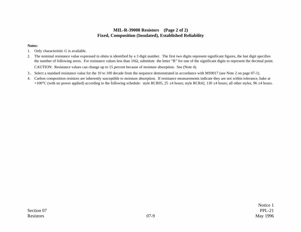
Notice 1Section 07 PPL-21Resistors 07-9 May 1996
MIL-R-39008 Resistors (Page 2 of 2)Fixed, Composition (Insulated), Established Reliability
Notes:1. Only characteristic G is available.2. The nominal resistance value expressed in ohms is identified by a 3 digit number. The first two digits represent significant figures, the last digit specifies
the number of following zeros. For resistance values less than 10Ω, substitute the letter “R” for one of the significant digits to represent the decimal point.
CAUTION: Resistance values can change up to 15 percent because of moisture absorption. See (Note 4).
3.. Select a standard resistance value for the 10 to 100 decade from the sequence demonstrated in accordance with MS9017 (see Note 2 on page 07-1).4. Carbon composition resistors are inherently susceptible to moisture absorption. If resistance measurements indicate they are not within tolerance, bake at
+100°C (with no power applied) according to the following schedule: style RCR05, 25 ±4 hours; style RCR42, 130 ±4 hours; all other styles, 96 ±4 hours.

Notice 1Section 07 PPL-21Resistors 07-10 May 1996
MIL-R-39009 Resistors (Page 1 of 2)Fixed, Wirewound (Power Type, Chassis Mounted), Established Reliability
Part Number Explanation:
RER XX X XXX X X
MIL-R-39009 Size Resistance Tolerance Significant Figures Number of Zeros Failure Rate(% per 1000 hrs.)
Style F = ±1.0% Resistance (Notes 1, 2) P = 0.1RER identifies established R = 0.01reliability, chassis mounted, power-type, wirewound, fixed resistors.“XX” represents a number which identifiesthe size and power rating of the resistors.
Characteristics
(Note 3) Resistance (Ohms)
Part Number ControlSpecification
Style Size Rated Powerat +25°°C
Range(Note 4)
Tolerance FRL
(Watts) Minimum Maximum (±±%) Grade 1 Grade 2
RER60FXXXXXRER65FXXXXXRER70FXXXXXRER75FXXXXX
MIL-R-39009/1(inductive)
RER60RER65RER70RER75
5.010.020.030.0
0.103.32K5.62K
12.1K39.2K 1.0 R P
RER40FXXXXXRER45FXXXXXRER50FXXXXXRER55FXXXXX
MIL-R-39009/2(noninductive)
RER40RER45RER50RER55
5.010.020.030.0
1.01.65K2.80K6.04K4.99K
See notes on page 07-11.

Notice 1Section 07 PPL-21Resistors 07-11 May 1996
MIL-R-39009 Resistors (Page 2 of 2)
Fixed, Wirewound (Power Type, Chassis Mounted), Established Reliability
Notes:1. For R > 100Ω, the first three digits are significant figures, the fourth is the number of following zeros. For R < 100Ω, the letter R replaces one of the
digits and is used as a decimal point; the remaining digits are significant figures.2. Select a standard resistance value for the 10 to 100 decade from Table II in MIL-R-39009 (see Note 2 on page 07-1).3. These aluminum-housed, chassis-mounted styles are assigned power ratings when mounted on test chassis areas of a specific size at an ambient
temperature of 25°C. Reference MIL-HDBK-978, Vol. 1, 3. 7.4. The maximum resistance value of preferred wirewound resistors is constrained by the size of the wire used in their construction. GSFC prohibits the use of
wire smaller than 0.001 inch (0.03 mm) in nominal diameter. Consult the applicable detail specification for wire size information.

Notice 1Section 07 PPL-21Resistors 07-12 May 1996
MIL-R-39015 Resistors (Note 1)Variable, Wirewound (Lead Screw Actuated), Established Reliability
Part Number Explanation:
M39015 /X -XXX X X
MIL number indicating Specification Sheet Dash Number Terminal Type Failure RateMIL-R-39015 Signifies the nominal resistance L - Flexible insulated (% per 1000 hrs.)
value, maximum resolution, and wire leads P = 0.1the maximum rated ac and dc P - Printed circuit pinworking voltage. (base mount)
W - Printed circuit pin(edge mount)
X - Printed circuit pin(edge mount - alternate configuration)
CharacteristicsResistance (Ohms) Maximum Maximum
Part Number Control Specification Style SizeRated
Power at+85°°C
Tolerance Range(Note 2)
ResolutionRange
(%)
Rated VoltageRange(Volts)
FRL
(Note 3)
(Watts) (±±%) Min Max Min Max Min Max Grade 2
M39015/2-XXXXX MIL-R-39015/2 RTR22 0.75 5.0 100 10K 0.14 0.51 8.7 86.7 P
M39015/3-XXXXX MIL-R-39015/3 RTR24 0.75 5.0 10 5K 0.25 1.3 2.7 61.3 P
Notes:1. Parts covered by this specification may contain internal soldered connections that may reflow during installation. Special care must be exercised when
soldering to prevent internal solder reflow. Welded connections are recommended for space flight use. Consult the manufacturer for construction details.2. The maximum resistance value of preferred wirewound resistors is constrained by the size of the wire used in their construction. GSFC prohibits the use of
wire smaller than 0.001 inch (0.03 mm) in nominal diameter. Consult the applicable detail specification for wire size information.3. Variable resistors shall not be used for Grade 1 applications.

Notice 1Section 07 PPL-21Resistors 07-13 May 1996
MIL-R-39017 ResistorsFixed, Film (Insulated), Established Reliability
Part Number Explanation:
RLR XX C XXX X X X
MIL-R-39017 Size Terminal Significant Number of Zeros Resistance Failure RateC - solderable/weldable Figures Tolerance (% per 1000 hrs.)
Style Resistance (Notes 1, 2) F = ±1.0% P = 0.1RLR identifies established G = ±2.0% R = 0.01reliability, insulated, fixed film, S = 0.001resistors. “XX” represents a numberwhich identifies the size and powerrating of the resistors.
Characteristics
Resistance (Ohms)
Part Number ControlSpecification
StyleSize
Rated Powerat +70°°C
Range(Note 3)
Tolerance MaximumVoltage
FRL
(Note 4) (Watts) Min Max (±±%) (Vdc) Grade 1 Grade 2
RLR05CXXXXXXRLR07CXXXXXX
MIL-R-39017/5MIL-R-39017/1
RLR05RLR07
1/81/4
4.710.0
1.0M10.0M 1.0, 2.0
200250 S P or R
RLR20CXXXXXXRLR32CXXXXXX
MIL-R-39017/2MIL-R-39017/3
RLR20RLR32
1/21
4.310.0
3.01M1.0M
350500
Notes:1. For R > 100Ω, the first three digits are significant figures, the fourth is the number of following zeros. For R < 100Ω, the letter R replaces one of the
digits and is used as a decimal point; the remaining digits are significant figures.2. Select a standard resistance value for the 10 to 100 decade from Table V in MIL-R-39017 (see Note 2 on page 07-1).3. The maximum resistance value presently available for resistors procured to FRL “S” is currently limited as follows:
RLR05 = .301M maximum; RLR 07 = 3.01M maximum.

Notice 1Section 07 PPL-21Resistors 07-14 May 1996
MIL-R-55182 Resistors (Page 1 of 3)Fixed, Film, Established Reliability
Part Number Explanation:
RNX XX X XXX(XX) X X X
MIL-R-55182 Size Characteristic Significant Figures Number of Zeros Resistance Failure RateTolerance (% per 1000 hrs.)
Style C = Hermetic (±50 ppm/°C) Resistance (Notes 1, 2) V = ±0.005% P = 0.1RNX identifies established E = Hermetic (±25 ppm/°C) T = ±0.01% R = 0.01reliability, film, fixed resistors H = Nonhermetic (±50 ppm/°C) A = ±0.05% S = 0.001
where: J = Nonhermetic (±25 ppm/°C) B = ±0.1%C = solderable/weldable terminal K = Nonhermetic (±100 ppm/°C) D = ±0.5%N = weldable terminal Y = Nonhermetic (Note 3) F = ±1.0%R = solderable terminal (±5 ppm/°C, up to +125°C)
(±10 ppm/°C, +125°C to +175°C)
Resistance (Ohms)
Part Number ControlSpecification
StyleSize
Rated Powerat +125°°C
Characteristics Range Tolerance Max.Volts
FRL
(Note 4) (Watts) Min Max (Note 4) (Vdc) Grade 1 Grade 2
RNC50XXXXXXX MIL-R-55182/7 RNC50 0.05 H, J 10 796K B, D, F(Note 5) K 10 796K D, F
RNN50XXXXXXX MIL-R-55182/7 RNN50 0.05 H, J, K 10 301K FRNR50XXXXXXX MIL-R-55182/7 RNR50 0.05 H, J 10 796K B, D, F
K 10 796K D, FRNC55XXXXXXX MIL-R-55182/1 RNC55 0.1 C, E 200 100K B, D, F 200 S P or R
(Note 5) H, J 10 2M B, D, FK 10 2M D, F
RNN55XXXXXXX MIL-R-55182/1 RNN55 0.1 C, E 10 301K B, D, FH, J 10 1M B, D, FK 10 1M D, F
H, J, K 1M 2M FSee notes on page 07-16.

Notice 1Section 07 PPL-21Resistors 07-15 May 1996
MIL-R-55182 Resistors (Page 2 of 3)Fixed, Film, Established Reliability
Resistance (Ohms)
Part Number ControlSpecification
StyleSize
Rated Powerat +125°°C
Characteristics Range Tolerance Max.Volts
FRL
(Note 4) (Watts) Min Max (Note 4) (Vdc) Grade 1 Grade 2
RNR55XXXXXXX MIL-R-55182/1 RNR55 0.1 C, E 10 301K B, D, F 200H, J 10 2M B, D, FK 10 2M D, F
RNC60XXXXXXX MIL-R-55182/3 RNC60 0.125 C, E 200 200K B, D, F 250(Note 5) H, J 10 2M B, D, F
K 10 2M D, FH, J, K 2M 3.01M F
RNN60XXXXXXX MIL-R-55182/3 RNN60 0.125 C, E 10 301K B, D, F 250H, J 10 2M B, D, F S P or RK 10 2M D, F
H, J, K 2M 3.01M FRNR60XXXXXXX MIL-R-55182/3 RNR60 0.125 C, E 10 301K B, D, F 250
H, J 10 2M B, D, FK 10 2M D, F
H, J, K 2M 3.01M FRNC65XXXXXXX MIL-R-55182/5 RNC65 0.25 C, E, H, J, K 200 499K B, D, F 300 S
(Note 5) H, J 10 200 B, D, F Note 6H, J 499K 3.01M B, D, F
RNN65XXXXXXX MIL-R-55182/5 RNN65 0.25 C, E, H, J, K 200 499K B, D, F 300 S
See notes on page 07-16.

Notice 1Section 07 PPL-21Resistors 07-16 May 1996
MIL-R-55182 Resistors (Page 3 of 3)Fixed, Film, Established Reliability
Resistance (Ohms)
Part Number ControlSpecification
StyleSize
Rated Powerat +125°°C
Characteristics Range Tolerance Max.Volts
FRL
(Note 4) (Watts) Min Max (Note 4) (Vdc) Grade 1 Grade 2
RNR65XXXXXXX MIL-R-55182/5 RNR65 0.25 C, E, H, J, K 200 499K B, D, F 300 SH, J 10 200 B, D, F (Note 6)H, J 499K 3.01M B, D, F
RNC70XXXXXXX MIL-R-55182/6 RNC70 0.5 C, E 200 250K B, D, F 350 S(Note 5) H, J, K 200 250K B, D, F
RNN70XXXXXXX MIL-R-55182/6 RNN70 0.5 C, E 200 250K B, D, F 350 P or RH, J, K 200 250K B, D, F
RNR70XXXXXXX MIL-R-55182/6 RNR70 0.5 C, E 200 250K B, D, F 350H, J, K 200 250K B, D, F
RNC90XXXXXXX MIL-R-55182/9 RNC90 0.3 Y 4.99 16.0 B, D, F 30016.2 30.0 A, B, D, F (Note 6)30.1 49.9K V, T, A, B,
D, FNotes:1. All styles except RNC90 are expressed by four digits; for R > 100Ω, the first three digits are significant figures, the fourth is the number of following
zeros. For R < 100Ω, the letter R replaces one of the digits and represents a decimal point. Style RNC90 is expressed as five significant digits and a letter.For R < 1000Ω, the letter R is used as a decimal point. For values > 1000Ω but < 1.0 MΩ, the letter K is used to represent a decimal point and multiplier.All digits preceding and following the letter (R or K) of the group represent significant figures.
2. Select a standard resistance value for the 10 to 100 decade from Table IV in MIL-R-55182 (see Note 2 on page 07-1).3. Characteristic “Y” is only available in RNC90 style.4. All styles except RNC90 are electrostatic sensitive. For tolerance B (±0.1%), package in accordance with MIL-R-39032 as specified for field protection.5. GSFC does not consider type “C” terminal material to be readily weldable and recommends using type “N” material for welding. Types “C” and “R” may
be used for soldering. Style RNC90 is not available with “N” terminal material.6. Grade 1 parts currently are not available (see Note 1 on page 07-1).

Notice 1Section 07 PPL-21Resistors 07-17 May 1996
MIL-R-55342 RESISTORS (Page 1 of 2)Fixed, Film, Chip, Established Reliability
Part Number Explanation:
M55342 X XX X XXXX X
MIL number indicating Characteristic Specification Termination Material Resistance Value Failure RateMIL-R-55342 E = ±25ppm/°C Sheet Number B - Solderable, base and Tolerance (% per 1000 hrs.)
(Note 1) H = ±50ppm/°C metalization barrier (Notes 2, 3) P = 0.1K = ±100 ppm/°C metal, solder coated R = 0.01M =±300 ppm/°C C - Bondable, palladium S = 0.001
silverR - Solderable, pretinnedW - Bondable, gold
MIL Resistance Terminations Volt. Power FRLSheet Style Characteristics Range
(Ohms)Tolerance
(+%)One
SurfaceWrap-around
Rating(V)
Rating(mW)
Grade1
Grade2
55342/2 RM0505 E, H 100.0 - 0.200M 0.1 S, W B, R 40 25 (Note 4) PK, M 5.6 - 0.470M 1.0, 2.0, 5.0, 10.0 W B, C, R, U 40 50 S P
M55342/3 RM1005 E, H 100.0 - 0.298M 0.1 S, W B, R 40 50 (Note 4) PK, M 5.6 - 1.000M 1.0, 2.0, 5.0, 10.0 W B, C, R, U 40 100 S PE, H 100.0 - 0.499M 0.1 S, W B, R 40 100 (Note 4) P
55342/4 RM1505 K 5.6 - 2.000M 1.0, 2.0, 5.0, 10.0 W B, C, R, U 40 150 S PM 5.6 - 4.700M 1.0, 2.0, 5.0, 10.0 W B, C, R, U
See notes on page 07-18.
Tol. Multiplier Symbol0.1 X 1 A0.1 X 1,000 B0.1 X1,000,000 C1.0 X 1 D1.0 X 1,000 E1.0 X 1,000,000 F2.0 X 1 G2.0 X 1,000 H2.0 X 1,000,000 T5.0 X 1 J5.0 X 1,000 K5.0 X 1,000,000 L
10.0 X 1 M10.0 X 1,000 N10.0 X 1,000,000 P

Notice 1Section 07 PPL-21Resistors 07-18 May 1996
MIL-R-55342 RESISTORS (Page 2 of 2)Fixed, Film, Chip, Established Reliability
MIL Resistance Terminations Volt. Power FRLSheet Style Characteristics Range
(Ohms)Tolerance
(+%)One
SurfaceWrap-around
Rating(V)
Rating(mW)
Grade1
Grade2
E, H 100.0 - 1.000M 0.1 (Note 4) B, R 40 200 (Note 4) P55342/5 RM2208 K 5.6 - 2.000M 1.0, 2.0, 5.0, 10.0 W B, C, R 40 225 S P
M 5.6 - 15.000M 1.0, 2.0, 5.0, 10.0 W B, C, R55342/6 RM0705 E, H 100.0 - 0.298M 0.1 S, W B, R 40 50 (Note 4) P
K, M 5.6 - 1.000M 1.0, 2.0, 5.0, 10.0 W B, C, R, U 40 100 S P55342/7 RM1206 E, H 100.0 - 0.499M 0.1 S B, R 100 125 (Note 4) P
K, M 5.6 - 1.000M 1.0, 2.0, 5.0, 10.0 (Note 4) B, C, R, U 100 250 S PE, H 100.0 - 1.000M 0.1 (Note 4) B, R 150 500 (Note 4) P
55342/8 RM2010 K 5.6 - 2.000M 1.0, 2.0, 5.0, 10.0 (Note 4) B, C, R 150 800 (Note 4) PM 5.6 - 15.000M 1.0, 2.0, 5.0, 10.0 (Note 4) B, C, R
E, H 100.0 - 1.000M 0.1 (Note 4) B, R 200 500 (Note 4) P55342/9 RM2512 K 5.6 - 2.000M 1.0, 2.0, 5.0, 10.0 (Note 4) B, C, R 200 1000 S P
M 5.6 - 15.000 M 1.0, 2.0, 5.0, 10.0 (Note 4) B, C, R55342/10 RM1010 K 5.6 - 5.600M 1.0, 2.0, 5.0, 10.0 (Note 4) B, R 40 500 S P
Notes:1. MIL-R-55342/7 resistor part numbers begin D55342; all others begin M55342.2. Nominal Resistance in ohms is identified by four characters consisting of three digits and a letter. All digits, whether preceding or following the letter, are
significant. The letter, inserted in a standard resistance value, is used simultaneously as a decimal point, multiplier, and resistance tolerance indicator asshown in the subtable.
3. Select a standard resistance value for the 10 to 100 decade from Table V in MIL-R-55342 (see Note 2 on page 07-1).4. Grade 1 part is not available.

Notice 1Section 07 PPL-21Resistors 07-19 May 1996
MIL-R-83401 Resistors (Notes 1, 2) (Page 1 of 2)Networks, Fixed, Film
Part Number Explanation:
M83401 XX X XXXX X X
MIL number indicating Specification Sheet Characteristic (Note 2) Resistance Tolerance SchematicMIL-R-83401 Number C = ±50 ppm/°C (hermetic) (Notes 3, 4) B = ±0.1% G = ±2.0% (Note 5)
H, V = ±50 ppm/°C (nonhermetic) D = ±0.5% J = ±5.0% A, BK = ±100 ppm/°C (nonhermetic) F = ±1.0% C, GM = ±300 ppm/°C (nonhermetic)
Resistance (Ohms) Max. Rated PowerPart Number
(Note 6)Control
SpecificationStyle Pins/
PackageCharac-teristic
Schematic Range Tolerance Voltage/Element
Range at +25°C(Watts) (Note 7)
Min Max (Vdc) Element NetworkM8340101XXXXXXX MIL-R-83401/1 RZ010 14/DIP C, V A 100 10K B, D, F, G, J 100 0.05-0.2 0.65-1.4
H A 50 100K B, D, F, G, JH B 50 70K B, D, F, G, JK A, B 27.4 50 F, G, JM A, B 10 50 F, G, JK, A, B 50 100K B, D, F, G, JM A, B 50 70K B, D, F, G, JK A, B 100K 1M F, G, JM A, B 70K 1M F, G, J
M8340102XXXXXXX MIL-R-83401/2 RZ020 16/DIP C, V A 100 10K B, D, F, G, J 100 0.05-0.2 0.75-1.6H A 50 100K B, D, F, G, JH B 50 70K B, D, F, G, JK A, B 27.4 50 F, G, JM A, B 10 50 F, G, JK, A, B 50 100K B, D, F, G, JM A, B 50 70K B, D, F, G, JK A, B 100K 1M F, G, JM A, B 70K 1M F, G, J
See notes on page 07-20.

Notice 1Section 07 PPL-21Resistors 07-20 May 1996
MIL-R-83401 Resistors (Notes 1, 2) (Page 2 of 2)Networks, Fixed, Film
Resistance (Ohms) Max. Rated PowerPart Number
(Note 6)Control
SpecificationStyle Pins/
PackageCharac-teristic
Schematic Range Tolerance Voltage/Element
Range at +25°C(Watts) (Note 7)
Min Max (Vdc) Element NetworkM8340103XXXXXXX MIL-R-83401/3 RZ030 14/ H A, B 150 51.1K D 50 0.025- 0.325-
FLAT H A, B 150 121K F, G, J 0.05 0.35K A, B 150 51.1K DK A, B 150 121K F, G, JM A,B 100 51.1K D
K, M A, B 10 1M F, G, JM8340107XXXXXX MIL-R-83401/7 RZ070 6/SIP H C, G 100 100K B, D, F, G, J 50 0.12 0.36-0.6
K, M C, G 100 100K B, DK, M C, G 10 1M F, G, J
M8340108XXXXXX MIL-R-83401/8 RZ080 8/SIP H C, G 100 100K B, D, F, G, J 50 0.12 0.48-0.84K, M C, G 100 100K B, DK, M C, G 10 1M F, G, J
M8340109XXXXXX MIL-R-83401/9 RZ090 10/SIP H C, G 100 100K B, D, F, G, J 50 0.12 0.60-1.08K, M C, G 100 100K B, DK, M C, G 10 1M F, G, J
Notes:1. Parts covered by this specification may contain internal soldered connections that may reflow during installation. Special care must be exercised when
soldering to prevent internal solder reflow. Welded connections are recommended for space flight use. Consult the manufacturer for construction details.2. Parts manufactured with internal solder terminations shall be subjected to additional testing in accordance with Table 07 of Appendix A.3. For R > 100 Ω, the first three digits are significant figures, the fourth is the number of following zeros. For R < 100 Ω, the letter R replaces one of the
digits and is used as a decimal point; the remaining digits are significant figures.4. Select a standard resistance value for the 10 to 100 decade from Table IV in MIL-R-83401 (see Note 2 on page 07-1).5. See MIL-R-83401 for schematic details.6 Parts are acceptable for Grade 2 applications.7 See the applicable detail specification to determine power ratings for characteristic/schematic combinations.

Notice 1Section 08 PPL-21Diodes 08-1 May 1996
Summary of Preferred Diodes
Description Refer toPage No.
Power Rectifier 08-2Shottky Barrier 08-3
Fast Recovery Rectifier 08-3Switching 08-5
Zener 08-6Voltage Reference 08-9
High Voltage 08-10Bi-Directional Transient Suppressor 08-11Unidirectional Transient Suppressor 08-13
Thyristor (SCRs) 08-17Current Regulator 08-18
Varactor 08-19Full Wave Bridge Rectifiers 08-20
Multiple Diode Array 08-21Light Emitting 08-21Small Signal 08-22

Notice 1Section 08 PPL-21Diodes 08-2 May 1996
DiodesMIL-S-19500 Part Number Explanation:
JAN XXX 1N XXXX X X -1
Military Quality Level Component ID Number A or B= Modified U = Unleaded MetallugicalDesignator S = Grade 1 Designator for Version Devices Bonding
TXV = Grade 2 Diodes
Power Rectifiers (Notes 1, 2)IO IR at VRWM
JAN Part No. MIL-S-19500 VRWM (Note 3) VFM at IF (µµA dc) trr Case(Vpk) (A) (Vpk) (A) 25°°C 150°°C (ns)
1N1202A /260 200 12 1.35 38 50 1000 DO41N1186 /297 200 35 1.4 110 3000 DO51N5550* /420 200 3 1.6 9 1.0 75 2000 DO141N1204A /260 400 12 1.35 38 50 1000 DO41N1188 /297 400 35 1.4 110 3000 DO51N5551 U * /420 400 3 1.6 9 1 75 2000 DO141N5616 U * /427 400 1 1.3 3 0.5 25 2000 DO351N1206A /260 600 12 1.35 38 50 1000 DO41N1190 /297 600 35 1.4 110 3000 DO51N5552 U * /420 600 3 1.6 9 1 75 2000 DO141N5618 U * /427 600 1 1.3 3 0.5 25 2000 DO351N3671A /260 800 12 1.35 38 50 1000 DO41N3766 /297 800 35 1.4 110 3000 DO51N5553 U * /420 800 3 1.6 9 1 75 2000 DO141N5620 U /427 800 1 1.3 3 .5 25 2000 DO351N3673A /260 1000 12 1.35 38 50 1000 DO41N3768 /297 1000 35 1.4 110 3000 DO51N5554 U * /420 1000 3 1.6 9 1 75 2000 DO41N5622 U /427 1000 1 1.3 3 0.5 25 2000 DO351N4245 thru 1N4249 /286 200 to 1000 1 5000 (Note 4)1N6073 thru 1N6081 /503 50 to 150 3.0 to 12 30
See notes on page 08-22.

Notice 1Section 08 PPL-21Diodes 08-3 May 1996
Schottky Barrier Rectifiers (Notes 1, 2)
JAN Part No. MIL-S-19500IO
(Note 3) VR VFM1 at IFM VFM2 at IFM Case
(A) (Vdc) (Vpk) (Apk) (Vpk) (Apk)
1N6391 /553 22.5 45 0.68 50 0.48 5 DO-41N6392 /554 54 45 0.82 120 0.68 60 DO-51N6492 /567 4.5 45 0.68 4 0.56 2 TO39
Fast Recovery Rectifiers (Notes 1, 2) (Page 1 of 2)
IO at
JAN Part No. MIL-S-19500 trr VRWM
75°C(Note 3) VFM at IF
IR at VRWM
(µµA dc) Case(ns) (Vpk) (A) (Vpk) (Apk) 25°°C 150°°C
1N3911 /308 15 200 30 1.4 50 15 60001N5804U* /477 25 100 2.5 0.975 2.5 1 501N5806U* /477 25 150 2.5 0.975 2.5 1 501N5802* /479 25 50 2.5 0.975 2.5 1 501N5807* /477 30 50 6 0.925 6.0 5.0 1501N5809* /477 30 100 6 0.925 6 5 1501N5811* /477 30 150 6 0.925 6 5 1501N6620U /585 30 200 2.0 1.6 2 0.5 1501N6621U /585 30 400 2.0 1.6 2 0.5 150 (Note 4)1N6622U /585 30 600 2.0 1.6 2 0.5 1501N6626U /590 30 200 4 1.5 2.5 2 5001N6627U /590 30 400 4 1.5 4 2 5001N6628U /590 30 600 4 1.5 4 2 5001N5812 /478 35 50 20 0.86 10 10 751N5814 /478 35 100 20 0.86 10 10 751N5816 /478 35 150 20 0.86 10 10 751N6305 /550 50 100 70 0.975 70 25 30001N6306 /550 50 150 70 0.975 70 25 30001N6623U /585 50 800 1.5 1.8 2 0.5 1501N6629U /590 50 800 3 1.7 4 2 500
See notes on page 08-22.

Notice 1Section 08 PPL-21Diodes 08-4 May 1996
Fast Recovery Rectifiers (Notes 1, 2) (Page 2 of 2)
IO at
JAN Part No. MIL-S-19500 trr VRWM
75°C(Note 3) VFM at IF
IR at VRWM
(µµA dc) Case(ns) (Vpk) (A) (Vpk) (Apk) 25°°C 150°°C
1N6625U /585 60 1000 1.5 1.95 2 1 2001N6631U /590 60 1000 2.5 1.95 3 4 6001N4942 /359 150 200 1 1N4944 /359 150 400 1 1N5416* /411 150 100 3 1.2 9 1 201N5417U* /411 150 200 3 1.2 9 1 201N5415* /411 150 200 3 1.2 9 1 201N5418U* /411 150 400 3 1.2 9 1 201N5615U* /429 150 200 1 1.6 3 0.5 25 (Note 4)1N5617U* /429 150 400 1 1.6 3 0.5 251N3891 /304 200 200 12 1.5 38 15 20001N3893 /304 200 400 12 1.5 38 15 20001N3913 /308 200 400 30 1.4 50 15 60001N4946 /359 250 600 1 1N4947 /359 250 800 1 1N5419U* /411 250 500 3 1.2 9 1 201N5619U* /429 250 600 1 1.6 3 0.5 251N5621U* /429 300 800 1 1.6 3 0.5 251N5623U* /429 300 1000 1 1.6 3 0.5 251N5420U* /411 400 600 3 1.2 9 1 201N4948 /359 500 1000 1
See notes on page 08-22.

Notice 1Section 08 PPL-21Diodes 08-5 May 1996
Switching Diodes (Notes 1, 2)
IR at VRWM
JAN Part No. MIL-S-19500 trr VRWM (µµA) VF at IF C Case(ns) (Vpk) 25°°C 150°°C (Vdc) (mA) (PF)
1N5719 /443 - 100 0.25 15 1 100 0.31N5711U /444 - 50 0.2 200 1 15 21N5712-1 /445 - 16 0.15 100 1 35 21N3595 /241 0.03 125 0.01 3 1 100 8.01N4454-1 /144 4 50 0.1 100 1 10 21N3600 /231 4 50 0.1 100 0.75 10 2.51N4153-1 /337 4 50 0.05 50 0.75 10 2 (Note 4)1N4153 /337 4 50 0.05 50 0.81 10 21N6638U /578 4.5 125 0.5 100 1.1 200 21N4148-1 /116 5 75 0.5 100 5 50 41N4531 /116 5 75 0.5 50 1.2 100 41N6642U* /578 5 75 0.5 100 1.2 100 51N4150-1 /231 6 50 0.1 100 0.74 10 2.51N6643U* /578 6 50 0.5 160 1.2 100 51N4938-1 /169 50 175 0.1 100 1 100 5
See notes on page 08-22.

Notice 1Section 08 PPL-21Diodes 08-6 May 1996
Zener Diodes (Notes 1, 2) (Page 1 of 3)
JAN Part No. (Listed by Detail Specification and PT)MIL-S-19500 /127 /117 /435 /533 /406 /356 /272 /124 /114
Power (Note 3) 400 mW 400 mW 400 mW 500 mW 1.5 W 5 W 10 W 10 W 50 WCase Axial Axial Axial Axial Axial Axial DO4 DO4 TO3
Vz Nominal (Vdc)
1.8 1N4614-12.0 1N4615-12.2 1N4616-12.4 1N4370A-1 1N4617-1 1N63092.7 1N4371A-1 1N4618-1 1N63103.0 1N4372A-1 1N4619-1 1N63113.3 1N746A-1 1N4620-1 1N6312 1N64853.6 1N747A-1 1N4621-1 1N6313 1N64863.9 1N748A-1 1N4622-1 1N6314 1N6487 1N3993A 1N4557B4.3 1N749A-1 1N4623-1 1N6315 1N6488 1N3994A 1N4558B4.7 1N750A-1 1N4624-1 1N6316 1N6489 1N3995A 1N4559B5.1 1N751A-1 1N4625-1 1N6317 1N6490 1N3996A 1N4560B5.6 1N752A-1 1N4626-1 1N6318 1N6491 1N5968 1N3997A 1N4561B6.2 1N753A-1 1N4627-1 1N6319 1N4460 1N5969 1N3998A 1N4562B6.8 1N754A-1* 1N4099-1 1N6320* 1N4461 1N4954* 1N3999A 1N2970B 1N2804B7.5 1N755A-1* 1N4100-1 1N6321* 1N4462 1N4955* 1N4000A 1N2971B 1N2805B8.2 1N756A-1* 1N4101-1 1N6322* 1N4463 1N4956* 1N2972B 1N2806B8.7 1N4102-19.1 1N757A-1* 1N4103-1 1N6323* 1N4464 1N4957* 1N2973B 1N2807B10.0 1N758A-1* 1N4104-1 1N6324* 1N4465 1N4958* 1N2974B 1N2808B11.0 1N962B-1 1N4105-1 1N6325* 1N4466 1N4959* 1N2975B 1N2809B12.0 1N759A-1* 1N963B-1 1N4106-1 1N6326* 1N4467 1N4960* 1N2976B 1N2810B13.0 1N964B-1 1N4107-1 1N6327* 1N4468 1N4961* 1N2977B 1N2811B14.0 1N4108-1
See notes on page 08-22.

Notice 1Section 08 PPL-21Diodes 08-7 May 1996
Zener Diodes (Notes 1, 2) (Page 2 of 3)
JAN Part No. (Listed by Detail Specification and PT)MIL-S-19500 /127 /117 /435 /533 /406 /356 /272 /124 /114
Power (Note 3) 400 mW 400 mW 400 mW 500 mW 1.5 W 5 W 10 W 10 W 50 WCase Axial Axial Axial Axial Axial Axial DO4 DO4 TO3
Vz Nominal (Vdc)
15.0 1N965B-1 1N4109-1 1N6328* 1N4469 1N4962* 1N2979B 1N2813B16.0 1N966B-1 1N4110-1 1N6329* 1N4470 1N4963* 1N2980B 1N2814B17.0 1N4111-118.0 1N967B-1 1N4112-1 1N6330* 1N4471 1N4964* 1N2982B 1N2816B19.0 1N4113-120.0 1N968B-1 1N4114-1 1N6331* 1N4472 1N4965* 1N2984B 1N2818B22.0 1N969B-1 1N4115-1 1N6332* 1N4473 1N4966* 1N2985B 1N2819B24.0 1N970B-1 1N4116-1 1N6333* 1N4474 1N4967* 1N2986B 1N2820B25.0 1N4117-127.0 1N971B-1 1N4118-1 1N6334* 1N4475* 1N4968* 1N2988B 1N2822B28.0 1N4119-130.0 1N972B-1 1N4120-1 1N6335* 1N4476* 1N4969* 1N2989B 1N2823B33.0 1N973B-1 1N4121-1 1N6336* 1N4477* 1N4970* 1N2990B 1N2824B36.0 1N974B-1 1N4122-1 1N6337 1N4478* 1N4971* 1N2991B 1N2825B39.0 1N975B-1 1N4123-1 1N6338 1N4479* 1N4972* 1N2992B 1N2826B43.0 1N976B-1 1N4124-1 1N6339 1N4480* 1N4973* 1N2993B 1N2827B47.0 1N977B-1 1N4125-1 1N6340 1N4481* 1N4974* 1N2995B 1N2829B51.0 1N978B-1 1N4126-1 1N6341 1N4482* 1N4975* 1N2997B 1N2831B56.0 1N979B-1 1N4127-1 1N6342 1N4483* 1N4976* 1N2999B 1N2832B60.0 1N4128-162.0 1N980N-1 1N4129-1 1N6343 1N4484* 1N4977* 1N3000B 1N2833B68.0 1N981B-1 1N4130-1 1N6344 1N4485* 1N4978* 1N3001B 1N2834B75.0 1N982B-1 1N4131-1 1N6345 1N4486* 1N4979* 1N3002B 1N2835B82.0 1N983B-1 1N4132-1 1N6346 1N4487* 1N4980* 1N3003B 1N2836B87.0 1N4133-191.0 1N984B-1 1N4134-1 1N6347 1N4488* 1N4981* 1N3004B 1N2837B100.0 1N985B-1 1N4135-1 1N6348 1N4489* 1N4982* 1N3005B 1N2838B
See notes on page 08-22.

Notice 1Section 08 PPL-21Diodes 08-8 May 1996
Zener Diodes (Notes 1, 2) (Page 3 of 3)
JAN Part No. (Listed by Detail Specification and PT)MIL-S-19500 /127 /117 /435 /533 /406 /356 /272 /124 /114
Power (Note 3) 400 mW 400 mW 400 mW 500 mW 1.5 W 5 W 10 W 10 W 50 WCase Axial Axial Axial Axial Axial Axial DO4 DO4 TO3
Vz Nominal (Vdc)
110.0 1N986B-1 1N6349 1N4490* 1N4983* 1N3007B 1N2840B120.0 1N987B-1 1N6350 1N4491* 1N4984* 1N3008B 1N2841B130.0 1N988B-1 1N6351 1N4492* 1N4985* 1N3009B 1N2842B150.0 1N989B-1 1N6352 1N4493* 1N4986* 1N3011B 1N2843B160.0 1N990B-1 1N6353 1N4494* 1N4987* 1N3012B 1N2844B180.0 1N991B-1 1N6354 1N4495* 1N4988* 1N3014B 1N2845B200.0 1N992B-1 1N6355 1N4496* 1N4989* 1N3015B 1N2846B220.0 1N4990*240.0 1N4991*270.0 1N4992*300.0 1N4993*330.0 1N4994*360.0 1N4995*390.0 1N4996*
See notes on page 08-22.

Notice 1Section 08 PPL-21Diodes 08-9 May 1996
Voltage Reference Diodes (Notes 1, 2)
Reference VoltageVR Dynamic Impedance
JANS Part No. MIL-S-19500 Min Max Z at IZ Case(Vdc) (Vdc) (Ohms) (mA)
1N821-1* /159 5.89 6.51 15 7.5 DO-71N823-1* /159 5.89 6.51 15 7.5 DO-71N825-1* /159 5.89 6.51 15 7.5 DO-71N827-1* /159 5.89 6.51 15 7.5 DO-71N829-1* /159 5.89 6.51 15 7.5 DO-71N4565A-1* /452 6.08 6.72 200 0.5 DO-71N4566A-1* /452 6.08 6.72 200 0.5 DO-71N4567A-1* /452 6.08 6.72 200 0.5 DO-71N4568A-1* /452 6.08 6.72 200 0.5 DO-71N4569A-1* /452 6.08 6.72 200 0.5 DO-71N4570A-1* /452 6.08 6.72 100 1 DO-71N4571A-1* /452 6.08 6.72 100 1 DO-71N4572A-1* /452 6.08 6.72 100 1 DO-71N4573A-1* /452 6.08 6.72 100 1 DO-71N4574A-1* /452 6.08 6.72 100 1 DO-71N3154-1 /158 7.98 8.82 15 10 DO-71N3155-1 /158 7.98 8.82 15 10 DO-71N3156-1 /158 7.98 8.82 15 10 DO-71N3157-1 /158 7.98 8.82 15 10 DO-71N935B-1 /156 8.55 9.45 20 7.5 DO-71N937B-1 /156 8.55 9.45 20 7.5 DO-71N938B-1 /156 8.55 9.45 20 7.5 DO-71N939B-1 /156 8.55 9.45 20 7.5 DO-71N940B-1 /156 8.55 9.45 20 7.5 DO-71N941B-1 /157 11.12 12.28 30 7.5 DO-71N943B-1 /157 11.12 12.28 30 7.5 DO-71N944B-1 /157 11.12 12.28 30 7.5 DO-71N945B-1 /157 11.12 12.28 30 7.5 DO-7
See notes on page 08-22.

Notice 1Section 08 PPL-21Diodes 08-10 May 1996
High Voltage Diodes (Notes 1, 2)
IO VF IR at VRWM
JAN Part No. MIL-S-19500 VRWM (Note 3) trr At IO (µµA) Case(Vdc) (A) (ns) (Vdc) 25°°C 150°°C
1N6520 /576 1,500 0.5 70 3 0.5 1501N6528 /577 1,500 0.25 70 3 0.1 501N6521 /576 2,000 0.5 70 3 0.5 1501N6529 /577 2,000 0.25 70 3 0.1 501N6522 /576 2,500 0.25 70 5 0.5 1501N6530 /577 2,500 0.1 70 7 0.1 501N6523 /576 3,000 0.25 70 5 0.5 150 (Note 4)1N6531 /577 3,000 0.1 70 7 0.1 501N6524 /576 4,000 0.15 70 7 0.5 1501N6532 /577 4,000 0.05 70 9 0.1 501N6525 /576 5,000 0.15 70 7 0.5 1501N6533 /577 5,000 0.05 70 9 0.1 501N6526 /576 7,500 0.1 70 12 0.5 1501N6534 /577 7,500 0.025 70 14 0.1 501N6527 /576 10,000 0.1 70 12 0.5 1501N6535 /577 10,000 0.025 70 14 0.1 50
See notes on page 08-22.

Notice 1Section 08 PPL-21Diodes 08-11 May 1996
Bi-Directional Transient Suppressor Diodes (Notes 1, 2) (Page 1 of 2)
JAN Part No.Breakdown
VoltageVBR (Vdc)
WorkingPeak
VoltageVM wkg
MaximumPeak Surge
VoltageVSM
MaximumPeak Surge
CurrentISM (Apk)
Case
500 W 1500 W Min Max (Vdc) (Vpk) 500W 1500W
1N6130A* 1N6139A 7.13 7.87 5.7 11.2 44.6 133.91N6104A* 1N6140A 7.79 8.61 6.2 12.1 41.3 124.01N6105A* 1N6141A 8.65 9.55 6.9 13.4 37.3 111.9
1N6106A* 1N6142A 9.50 10.50 7.6 14.5 34.5 103.41N6107A* 1N6143A 10.45 11.55 8.4 15.6 32.0 96.21N6108A* 1N6144A 11.40 12.60 9.1 16.9 29.6 88.8
1N6109A* 1N6145A 12.35 13.65 9.9 18.2 27.5 82.41N6110A* 1N6146A 14.25 15.75 11.4 21.0 23.8 71.41N6111A* 1N6147A 15.20 16.80 12.2 22.3 22.4 67.3
1N6112A* 1N6148A 17.10 18.90 13.7 25.1 19.9 59.81N6113A* 1N6149A 19.0 21.0 15.2 27.7 18.0 54.2 (Note 4)1N6114A* 1N6150A 20.9 23.1 16.7 30.5 16.4 49.2
1N6115A* 1N6151A 22.8 25.2 18.2 33.3 15.0 45.01N6116A* 1N6152A 25.7 28.3 20.6 37.4 13.4 40.11N6117A* 1N6153A 28.5 31.5 22.8 41.6 12.0 36.0
1N6118A* 1N6154A 31.4 34.6 25.1 45.7 10.9 32.81N6119A 1N6155A 34.2 37.8 27.4 49.9 10.0 30.11N6120A 1N6156A 37.1 40.9 29.7 53.6 9.3 28.0
1N6121A 1N6157A 40.9 45.1 32.7 59.1 8.5 25.41N6122A 1N6158A 44.7 49.3 35.8 64.6 7.7 23.21N6123A 1N6159A 48.5 53.5 38.8 70.1 7.1 21.4
See notes on page 08-22.
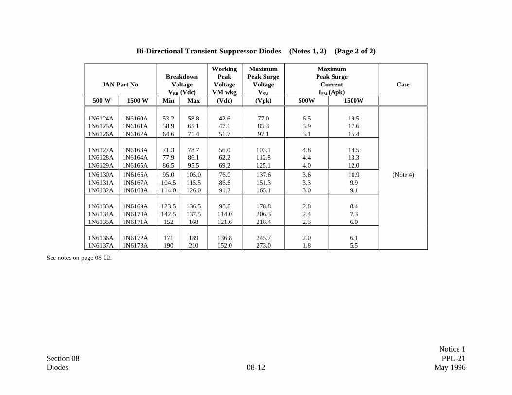
Notice 1Section 08 PPL-21Diodes 08-12 May 1996
Bi-Directional Transient Suppressor Diodes (Notes 1, 2) (Page 2 of 2)
JAN Part No.Breakdown
VoltageVBR (Vdc)
WorkingPeak
VoltageVM wkg
MaximumPeak Surge
VoltageVSM
MaximumPeak Surge
CurrentISM (Apk)
Case
500 W 1500 W Min Max (Vdc) (Vpk) 500W 1500W
1N6124A 1N6160A 53.2 58.8 42.6 77.0 6.5 19.51N6125A 1N6161A 58.9 65.1 47.1 85.3 5.9 17.61N6126A 1N6162A 64.6 71.4 51.7 97.1 5.1 15.4
1N6127A 1N6163A 71.3 78.7 56.0 103.1 4.8 14.51N6128A 1N6164A 77.9 86.1 62.2 112.8 4.4 13.31N6129A 1N6165A 86.5 95.5 69.2 125.1 4.0 12.01N6130A 1N6166A 95.0 105.0 76.0 137.6 3.6 10.9 (Note 4)1N6131A 1N6167A 104.5 115.5 86.6 151.3 3.3 9.91N6132A 1N6168A 114.0 126.0 91.2 165.1 3.0 9.1
1N6133A 1N6169A 123.5 136.5 98.8 178.8 2.8 8.41N6134A 1N6170A 142.5 137.5 114.0 206.3 2.4 7.31N6135A 1N6171A 152 168 121.6 218.4 2.3 6.9
1N6136A 1N6172A 171 189 136.8 245.7 2.0 6.11N6137A 1N6173A 190 210 152.0 273.0 1.8 5.5
See notes on page 08-22.

Notice 1Section 08 PPL-21Diodes 08-13 May 1996
Unidirectional Transient Suppressor Diodes (Notes 1, 2) (Page 1 of 4)
JAN Part No. BreakdownVoltage Working PeakTest Current
tp=300ms
MaximumClamping Voltage
at IP for
Maximum PeakPulse Current
IP CaseMIL-S-19500/434
1500 WattsV(BR) atIBR(min)
Reverse VoltageVRWM
Duty Cycle ≤≤ 2IBR
tp = 1 msVC(max)
tp = 20 µµstr = 8µµs
tp = 1mstr = 10µµs
(Vdc) (Vpk) (mA) (Vpk) (Apk) (Apk)
1N5610 33.0 30.5 1 47.6 193 32.0
1N5611 43.7 40.3 1 63.5 136 24.0 (Note 4)
1N5612 54.0 49.0 1 78.5 116 19.0
1N5613 191.0 175.0 1 265.0 33 5.7
MIL-S-19500/5001500 Watts
1N5555 33.0 30.5 1 47.5 193 32.0
1N5556 43.7 40.3 1 63.5 136 24.0
1N5557 54.0 49.0 1 78.5 116 19.0
1N5558 191.0 175.0 1 265.0 33 5.7
1N5907 6.0 5.0 1 8.5 1000 150.0
1N5629A 6.45 5.8 10 10.5 810 143.0
1N5630A 7.13 6.4 10 11.3 750 132.0 (Note 4)
1N5631A 7.79 7.02 10 12.1 700 124.0
1N5632A 8.65 7.78 1 13.4 630 112.0
1N5633A 9.5 8.55 1 14.5 585 103.5
1N5634A 10.5 9.4 1 15.6 545 96.0
1N5635A 11.4 10.2 1 16.7 510 90.0
1N5636A 12.4 11.1 1 18.2 465 82.0
1N5637A 14.3 12.8 1 21.2 400 71.0
See notes on page 08-22.

Notice 1Section 08 PPL-21Diodes 08-14 May 1996
Unidirectional Transient Suppressor Diodes (Notes 1, 2) (Page 2 of 4)
JAN Part No. BreakdownVoltage Working PeakTest Current
tp=300ms
MaximumClamping Voltage
at IP for
Maximum PeakPulse Current
IP CaseMIL-S-19500/500
1500 WattsV(BR) atIBR(min)
Reverse VoltageVRWM
Duty Cycle ≤≤ 2IBR
tp = 1 msVC(max)
tp = 20 µµstr = 8µµs
tp = 1mstr = 10µµs
(Vdc) (Vpk) (mA) (Vpk) (Apk) (Apk)
1N5638A 15.2 13.6 1 22.5 375 67.0
1N5639A 17.1 15.3 1 25.2 335 59.5
1N5640A 19.0 17.1 1 27.7 305 54.0
1N5641A 20.9 18.8 1 30.6 275 49.0
1N5642A 22.8 20.5 1 33.2 255 45.0
1N5643A 25.7 23.1 1 37.5 225 40.0
1N5644A 28.5 25.6 1 41.4 205 36.0 (Note 4)
1N5645A 31.4 28.2 1 45.7 185 33.0
1N5646A 34.2 30.8 1 49.9 170 30.0
1N5647A 37.1 33.3 1 53.9 155 28.0
1N5648A 40.9 36.8 1 59.3 145 25.3
1N5649A 44.7 40.2 1 64.8 130 23.2
1N5650A 48.5 43.6 1 70.1 120 21.4
1N5651A 53.2 47.8 1 77.0 110 19.5
1N5652A 58.9 53.0 1 85.0 100 17.7
1N5653A 64.6 58.1 1 92.0 90 16.3
1N5654A 71.3 64.1 1 103.0 82 14.6
1N5655A 77.9 70.1 1 113.0 75 13.3
1N5656A 86.5 77.8 1 125.0 68 12.0
1N5657A 95.0 85.5 1 137.0 62 11.0
See notes on page 08-22.
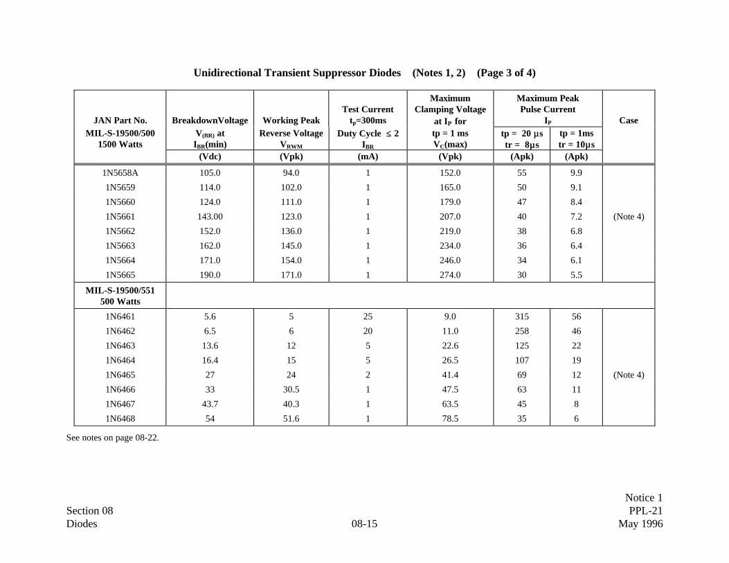
Notice 1Section 08 PPL-21Diodes 08-15 May 1996
Unidirectional Transient Suppressor Diodes (Notes 1, 2) (Page 3 of 4)
JAN Part No. BreakdownVoltage Working PeakTest Current
tp=300ms
MaximumClamping Voltage
at IP for
Maximum PeakPulse Current
IP CaseMIL-S-19500/500
1500 WattsV(BR) atIBR(min)
Reverse VoltageVRWM
Duty Cycle ≤≤ 2IBR
tp = 1 msVC(max)
tp = 20 µµstr = 8µµs
tp = 1mstr = 10µµs
(Vdc) (Vpk) (mA) (Vpk) (Apk) (Apk)
1N5658A 105.0 94.0 1 152.0 55 9.9
1N5659 114.0 102.0 1 165.0 50 9.1
1N5660 124.0 111.0 1 179.0 47 8.4
1N5661 143.00 123.0 1 207.0 40 7.2 (Note 4)
1N5662 152.0 136.0 1 219.0 38 6.8
1N5663 162.0 145.0 1 234.0 36 6.4
1N5664 171.0 154.0 1 246.0 34 6.1
1N5665 190.0 171.0 1 274.0 30 5.5
MIL-S-19500/551500 Watts
1N6461 5.6 5 25 9.0 315 56
1N6462 6.5 6 20 11.0 258 46
1N6463 13.6 12 5 22.6 125 22
1N6464 16.4 15 5 26.5 107 19
1N6465 27 24 2 41.4 69 12 (Note 4)
1N6466 33 30.5 1 47.5 63 11
1N6467 43.7 40.3 1 63.5 45 8
1N6468 54 51.6 1 78.5 35 6
See notes on page 08-22.

Notice 1Section 08 PPL-21Diodes 08-16 May 1996
Unidirectional Transient Suppressor Diodes (Notes 1, 2) (Page 4 of 4)
JAN Part No. BreakdownVoltage Working PeakTest Current
tp=300ms
MaximumClamping Voltage
at IP for
Maximum PeakPulse Current
IP CaseMIL-S-19500/552
1500 WattsV(BR) atIBR(min)
Reverse VoltageVRWM
Duty Cycle ≤≤ 2IBR
tp = 1 msVC(max)
tp = 20 µµstr = 8µµs
tp = 1mstr = 10µµs
(Vdc) (Vpk) (mA) (Vpk) (Apk) (Apk)
1N6469 5.6 5 50 9.0 945 167
1N6470 6.5 6 50 11.0 775 137
1N6471 13.6 12 10 22.6 374 66
1N6472 16.4 15 10 26.5 322 57 (Note 4)
1N6473 27 24 50 41.4 206 36.5
1N6474 33 30.5 1 47.5 190 32
1N6475 43.7 40.3 1 63.5 136 24
1N6476 54 51.6 1 78.5 106 19
See notes on page 08-22.

Notice 1Section 08 PPL-21Diodes 08-17 May 1996
Thyristors (SCRs) (Notes 1, 2)
JANS Part No. MIL-S-19500 IO at TC VRSM
IFSM
surge ton Toff VGTM IM Case
(A) °°C (Vpk) (A) (µµs) (µµs) (Vdc) (mA)
2N3027 /419 0.175 100 30 0.2 2 0.6 0.2 TO-182N3028 /419 0.175 100 60 0.2 2 0.6 0.2 TO-182N3029 /419 0.175 100 100 0.2 2 0.6 0.2 TO-182N2323A /276 0.22 80 75 15 1 0.35 TO-52N2324A /276 0.22 80 150 15 1 0.35 TO-52N2326A /276 0.22 80 300 15 1 0.35 TO-52N2328A /276 0.22 80 400 15 1 0.35 TO-52N2329 /276 0.22 80 500 15 1 0.35 TO-52N1774A /168 4.7 105 200 60 5 30 2 30 TO-642N1777A /168 4.7 105 400 60 5 30 2 30 TO-642N685 /108 16 65 200 150 5 30 3 80 TO-208MA2N688 /108 16 65 400 150 5 30 3 80 TO-208MA2N690 /108 16 65 600 150 5 40 3 80 TO-208MA
See notes on page 08-22.

Notice 1Section 08 PPL-21Diodes 08-18 May 1996
Current Regulator Diodes (Notes 1, 2)
Temperature Coefficient of IS
TCIP (%/°C)JAN Part No. MIL-S-19500 IP ZS ZK VL at –55°C at -25°C Case
(mA) (MΩΩ) (kΩΩ) (Vdc) Min Max Min Max1N5283 /463 0.22 25 2750 1 0.20 +1.35 -0.16 +0.70 DO-71N5284 /463 0.24 19 2350 1 +1.25 -0.11 +0.66 DO-71N5285 /463 0.27 14 1950 1 -0.10 +1.15 -0.12 +0.58 DO-71N5286 /463 0.30 9 1600 1 -0.15 +1.05 -0.15 +0.52 DO-71N5287 /463 0.33 6.6 1350 1 -0.20 +0.95 -0.16 +0.47 DO-71N5288 /463 0.39 4.1 1000 1.05 -0.30 +0.82 -0.20 +0.38 DO-71N5289 /463 0.43 3.3 870 1.05 -0.32 +0.75 -0.22 +0.33 DO-71N5290 /463 0.47 2.7 750 1.05 -0.35 +0.70 -0.23 +0.28 DO-71N5291 /463 0.56 1.9 560 1.10 -0.40 +0.55 -0.26 +0.20 DO-71N5292 /463 0.62 1.55 470 1.13 -0.42 +0.45 -0.27 +0.15 DO-71N5293 /463 0.68 1.35 400 1.15 -0.45 +0.40 -0.28 +0.12 DO-71N5294 /463 0.75 1.15 335 1.20 -0.50 +0.35 -0.30 +0.07 DO-71N5295 /463 0.82 1.00 290 1.25 -0.52 +0.27 -0.31 +0.03 DO-71N5296 /463 0.91 0.88 240 1.29 -0.56 +0.20 -0.32 DO-71N5297 /463 1.00 0.80 205 1.35 -0.58 +0.15 -0.34 DO-71N5298 /463 1.10 0.70 180 1.40 -0.60 +0.10 -0.36 DO-71N5299 /463 1.20 0.64 155 1.45 -0.63 +0.05 -0.37 DO-71N5300 /463 1.30 0.58 135 1.50 -0.65 -0.38 DO-71N5301 /463 1.40 0.54 115 1.55 -0.68 -0.39 DO-71N5302 /463 1.50 0.51 105 1.60 -0.70 -0.40 DO-71N5303 /463 1.60 0.475 92 1.65 -0.70 -0.40 DO-71N5304 /463 1.80 0.42 74 1.75 -0.72 -0.41 DO-71N5305 /463 2.00 0.395 61 1.85 -0.75 -0.42 DO-71N5306 /463 2.20 0.37 52 1.95 -0.76 -0.42 DO-71N5307 /463 2.40 0.345 44 2.00 -0.78 -0.43 DO-71N5308 /463 2.7 0.32 35 2.15 -0.80 -0.43 DO-71N5309 /463 3.0 0.30 29 2.25 -0.81 -0.43 DO-71N5310 /463 3.3 0.28 24 2.35 -0.82 -0.44 DO-71N5311 /463 3.6 0.265 20 2.5 -0.83 -0.44 DO-71N5312 /463 3.9 0.255 17 2.6 -0.84 -0.45 DO-71N5313 /463 4.3 0.245 14 2.75 -0.85 -0.45 DO-71N5314 /463 4.7 0.236 12 2.9 -0.86 -0.45 DO-7
See notes on page 08-22.

Notice 1Section 08 PPL-21Diodes 08-19 May 1996
Varactor Diodes (Notes 1, 2)
JAN Part No. MIL-S-19500Ct at4 Vdc
Capacitance Ratio (min.)Ct1@VR1, Ct2@ VR2
VoltageVRWM
Figure of Merit (Q)at VR = 4 Vdc Case
(pF) VR1
(Vdc)VR2
(Vdc)(Vdc) Q Freq (MHz)
1N5139A /383 6.8 2.7 4 60 60 350 1 DO-71N5461C /436 6.8 2.9 2 30 600 50 DO-71N5462C /436 8.2 2.95 2 30 600 50 DO-71N5140A /383 10 2.8 4 60 60 300 1 DO-71N5463C /436 10 2.95 2 30 550 50 DO-71N5141A /383 12 2.8 4 60 60 300 1 DO-71N5464C /436 12 2.95 2 30 550 50 DO-71N5142A /383 15 2.8 4 60 60 250 1 DO-71N5465C /436 15 2.95 2 30 550 50 DO-71N5143A /383 18 2.8 4 60 60 250 1 DO-71N5466C /436 18 3 2 30 500 50 DO-71N5467C /436 20 3 2 30 500 50 DO-71N5468C /436 22 3.05 2 30 500 50 DO-71N5144A /383 22 3.2 4 60 60 200 1 DO-71N5469C /436 27 3.05 2 30 500 50 DO-71N5145A /383 27 3.2 4 60 60 200 1 DO-71N5470C /436 33 3.05 2 30 500 50 DO-71N5146A /383 33 3.2 4 60 60 200 1 DO-71N5471C /436 39 3.05 2 30 500 50 DO-71N5147A /383 39 3.2 4 60 60 200 1 DO-71N5472C /436 47 3.05 2 30 400 50 DO-71N5148A /383 47 3.2 4 60 60 200 1 DO-71N5473C /436 56 3.1 2 30 300 50 DO-71N5473C /436 68 3.1 2 30 250 50 DO-71N5475C /436 82 3.1 2 30 225 50 DO-71N5476C /436 100 3.1 2 30 200 50 DO-7
See notes on page 08-22.
ct1
ct2
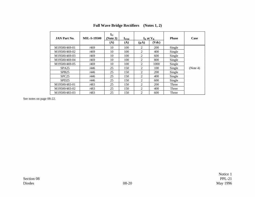
Notice 1Section 08 PPL-21Diodes 08-20 May 1996
Full Wave Bridge Rectifiers (Notes 1, 2)
JAN Part No. MIL-S-19500IO
(Note 3) IFSM IR at VR Phase Case(A) (A) (µµA) (Vdc)
M19500/469-01 /469 10 100 2 200 SingleM19500/469-02 /469 10 100 2 400 SingleM19500/469-03 /469 10 100 2 600 SingleM19500/469-04 /469 10 100 2 800 SingleM19500/469-05 /469 10 100 2 1000 Single
SPA25 /446 25 150 2 100 Single (Note 4)SPB25 /446 25 150 2 200 SingleSPC25 /446 25 150 2 400 SingleSPD25 /446 25 150 2 600 Single
M19500/483-01 /483 25 150 2 200 ThreeM19500/483-02 /483 25 150 2 400 ThreeM19500/483-03 /483 25 150 2 600 Three
See notes on page 08-22.

Notice 1Section 08 PPL-21Diodes 08-21 May 1996
Multiple Diode Arrays (Notes 1, 2)
JAN Part No. MIL-S-19500IO
(Note 3) VF at IF IR at VR Trr CT Case(mA) (Vdc) (mA) (uA) (Vdc) (ns) (pF)
1N5768 /474 300 1.5 500 0.1 40 20 4 FLAT1N5770 /474 300 1.5 500 0.1 40 20 8 FLAT1N5772 /474 300 1.5 500 0.1 40 20 8 FLAT1N5774 /474 300 1.5 500 0.1 40 20 8 FLAT1N6506 /474 300 1.5 500 0.1 40 20 4 DIP1N6507 /474 300 1.5 500 0.1 40 20 8 DIP1N6508 /474 300 1.5 500 0.1 40 20 8 DIP1N6509 /474 300 1.5 500 0.1 40 20 8 DIP1N6100 /474 300 1.0 100 0.025 20 5 4 FLAT1N6101 /474 300 1.0 100 0.025 20 5 4 DIP1N6510 /474 300 1.0 100 0.025 20 5 4 FLAT1N6511 /474 300 1.0 100 0.025 20 5 4 DIP
Light Emitting Diodes (Notes 1, 2)
JAN Part No. MIL-S-19500 Color Iv
C at VR = 0f = 9 MHz VFM
Wave Length (λλ)(nm) Case
(mcd) (PF) (Vdc) Min Max
1N6609 /519 RED 20 100 3 590 6951N6610 /520 YELLOW 20 100 3 550 6601N6611 /521 GREEN 20 100 3 525 6001N6495 /572 GREEN 0.8 100 3 525 5801N6493 /572 RED 1 100 3 595 695 (Note 4)1N6494 /572 YELLOW 1 100 3 570 5951N6499 /574 GREEN 0.5 500 25 525 5801N6497 /574 RED 0.5 500 20 595 6951N6498 /574 YELLOW 0.5 500 20 570 595
See notes on page 08-22.

Notice 1Section 08 PPL-21Diodes 08-22 May 1996
Small Signal Diodes (Notes 1, 2)
JAN Part No. MIL-S-19500IO
(Note 3) VRWM VFM1 at IFM1 Case
(A) (Vpk) (Vpk) (A)
1N645-1* /240 400 225 1.0 0.4 TO51N647-1* /240 400 400 1.0 0.4 TO51N649-1* /240 400 600 1.0 0.4 TO5
Notes:
1. An asterisk (*) next to the device number indicates that the part is available to both JANS and JANTXV assurance levels. The absence of the asteriskindicates that the part is available only to the JANTXV assurance level.
2. Except for non-cavity diodes, all JANTXV diodes must be PIND tested in accordance with Appendix A and are preferred Grade 2 parts.3. The average forward current, IO, is specified at different temperatures, ranging from 25°C to 150°C. The power rating for zener diodes may also be given
at different temperatures, ranging from 25°C to 150°C. Refer to detail specifications for exact test conditions.4. No standard JEDEC case outline is specified. Refer to detail specification for package outline.

Notice 1Section 09 PPL-21Transistors 09-1 May 1996
Summary of Preferred Transistors
DescriptionRefer toPage No.
NPN, Low Power 09-2
PNP, Low Power 09-3
NPN, High Power 09-4
PNP, High Power 09-6
RF 09-7
Quad, MOSFETs 09-7
N-Channel Power MOSFETs 09-8
P-Channel Power MOSFETs 09-10
PNP, Darlington 09-10
NPN, Darlington 09-11
N-Channel FETs 09-11
P-Channel FETs 09-12
Silicon Dual, Complementry 09-12
Optocouplers 09-13

Notice 1Section 09 PPL-21Transistors 09-2 May 1996
Transistors
MIL-S-19500 Part Number Explanation:
JAN XXX X YN XXXX X X
Military Designator Quality level Radiation Hardness Y = 1 less than ID Number A = Modified U- UnleadedS = Grade 1 Assurance the number of Version Devices
TXV = Grade 2 terminations
NPN Low Power Transistors (Notes 1, 2 ) (Page 1 of 2)
Maximum Ratings Primary Electrical Characteristics
JAN Part No. MIL-S-19500PT
TA=25°c IC VCBO VCEO VEBO hFE at IC VCE(sat)at IC Cobo Case(mW) (mA) (Vdc) (Vdc) (Vdc) Min/Max (mA) (Vdc) (mA) (pF)
2N2484* /376 360 50 60 60 6.0 200/500 0.01 0.3 1.0 5.0 TO182N2222AU* (Note 3) /255 500 800 75 50 6.0 100/300 150 1.0 500 8.0 TO182N3440* /368 800 1000 300 250 7.0 40/160 20 0.5 50 10 TO52N3439* /368 800 1000 450 350 7.0 40/160 20 0.5 50 10 TO52N3507 /349 1000 3000 80 50 5.0 30/150 1500 1.0 1500 40 TO52N3421* /393 1000 3000 125 80 8.0 40/120 1000 0.25 1000 150 TO52N3418 /393 1000 3000 80 60 8.0 20/60 1000 0.25 1000 150 TO52N3419 /393 1000 3000 80 80 8.0 20/60 1000 0.25 1000 150 TO52N3420 /393 1000 3000 80 60 8.0 40/20 1000 0.25 1000 150 TO5
See notes on page 09-13.
M = 3 x 10³ RAD (Si)D = 1 x 10⁴ RAD (Si)L = 5 x 10⁴RAD (Si)R = 1 x 10⁵ RAD (Si)F = 3 x 10⁵ RAD (Si)G = 6 x 10⁵ RAD (Si)H = 1 x 10⁶ RAD (Si)

Notice 1Section 09 PPL-21Transistors 09-3 May 1996
NPN Low Power Transistors (Notes 1, 2 ) (Page 2 of 2)
Maximum Ratings Primary Electrical Characteristics
JAN Part No. MIL-S-19500PT
TA=25°C IC VCBO VCEO VEBO hFE at IC VCE(sat)at IC Cobo Case(mW) (mA) (Vdc) (Vdc) (Vdc) Min/Max (mA) (Vdc) (mA) (pF)
2N5339 /560 1000 5000 100 100 6.0 60/240 2000 0.7 2000 250 TO392N5660 /454 1200 2000 250 200 6.0 40/120 500 0.4 1000 45 TO52N5662 /454 1200 2000 250 200 6.0 40/120 500 0.4 1000 45 TO52N5663 /454 1200 2000 250 200 6.0 40/120 500 0.4 1000 45 TO52N5666* /455 1200 5000 250 200 6.0 40/120 1000 0.4 3000 90 TO52N5667* /455 1200 5000 400 300 6.0 25/75 1000 0.4 3000 90 TO52N4150* /394 1500 10000 100 70 7.0 40/120 5000 0.6 5000 350 TO52N5237* /394 1500 10000 150 120 7.0 40/120 5000 0.6 5000 350 TO5
PNP Low Power Transistors (Notes 1, 2)
Maximum Ratings Primary Electrical Characteristics
JAN Part No. MIL-S-19500PT
TA=25°C IC VCBO VCEO VEBO hFE at IC VCE (sat) at IC Cobo Case(mW) (mA) (Vdc) (Vdc) (Vdc) Min/Max (mA) (Vdc) (mA) (pF)
2N4261* /511 200 30 15 15 4.5 30/150 10 0.15 1.0 2.0 TO722N2907AU* (Note 3) /291 400 600 60 60 5.0 100/300 150 1.6 500 8.0 TO18
2N2945A /382 400 100 25 20 25.0 70/--- 1.0 1.0 10 10 TO462N2946A /382 400 100 40 35 40.0 50/--- 1.0 2.0 10 10 TO462N5416 /485 750 1000 350 300 6.0 30/120 50 2.0 50 15 TO52N5415 /485 750 1000 200 200 6.0 30/120 50 2.0 50 15 TO5
2N3868* /350 1000 3000 60 60 4.0 30/150 1500 0.75 1500 120 TO52N3867* /350 1000 3000 40 40 4.0 40/200 1500 0.75 1500 120 TO52N3637* /357 1000 1000 175 175 5.0 100/300 50 0.9 50 10 TO52N5153* /545 1000 2000 100 80 5.5 70/200 2500 1.5 5000 250 TO392N6193* /561 1000 5000 100 100 6.0 60/240 2000 0.7 2000 300 TO39
See notes on page 09-13.

Notice 1Section 09 PPL-21Transistors 09-4 May 1996
NPN High Power Transistors (Notes 1, 2) (Page 1 of 2)
Maximum Ratings Primary Electrical Characteristics
JAN Part No. MIL-S-19500PT
TC=100°C IC VCBO VCEO VEBO hFE at IC VCE (sat) Case(W) (A) (Vdc) (Vdc) (Vdc) Min/Max (A) Max (mA)
2N5237* /394 5 10 150 120 7.0 40/120 5.0 0.6 5 TO32N5238* /394 5 10 200 170 7.0 40/120 5.0 0.6 5 TO32N3739 /402 10 3 325 300 6.0 40/200 0.1 2.5 0.25 TO662N5666* /455 15 5 250 200 6.0 40/120 0.5 1.2 3.0 TO662N5667* /455 15 5 400 300 6.0 40/120 1.0 1.2 3.0 TO662N5660 /454 20 2 250 200 6.0 40/120 0.5 1.2 0.4 TO662N3767 /518 25 4 100 80 6.0 40/160 0.5 1.0 0.5 TO662N2151 /277 30 2 150 100 6.0 40/120 1.0 0.1 1.0 TO592N3997* /374 30 5 100 80 8.0 80/240 1.0 2.0 5.0 TO112N2880* /315 30 5 110 80 8.0 40/120 1.0 0.25 1.0 STUD2N5664* /455 30 5 250 200 6.0 40/120 1.0 0.4 3.0 TO662N5665* /455 30 5 400 300 6.0 25/75 1.0 0.4 3.0 TO662N3749* /315 30 5 110 80 8.0 40/120 1.0 0.25 1.0 STUD2N3996* /374 30 5 100 80 8.0 40/120 1.0 2.0 5.0 TO112N3585 /384 35 2 500 300 7.0 25/100 1.0 0.75 1.0 TO662N3879 /526 35 7 120 75 8.0 20/180 4.0 1.2 4.0 TO662N2814 /415 50 10 120 80 5.5 50/150 1.0 0.5 5.0 TO612N5004 /534 58 5 100 80 6.0 70/200 2.5 1.5 5.0 TO592N3716 /408 85.7 10 100 80 7.0 30/120 3.0 1.0 5.0 TO662N5157 /371 100 3.5 700 500 7.0 30/90 1.0 0.8 1.0 TO32N3442 /370 117 10 160 140 7.0 20/70 3.0 1.0 3.0 TO32N5038* /439 140 20 150 90 7.0 50/200 2.0 1.0 12 TO32N5672 /488 140 30 150 120 7.0 20/100 15 0.75 15 TO32N5039* /439 140 20 125 75 7.0 30/150 2.0 1.0 12 TO32N6671 /536 150 8 450 300 8.0 10/80 1.0 1.0 5 TO32N5926 /447 200 50 150 120 10 20/80 20 0.6 50A TO-210AE2N5927 /440 200 100 150 120 10 30/120 20 0.75 70A TO-114
See notes on page 09-13.

Notice 1Section 09 PPL-21Transistors 09-5 May 1996
NPN High Power Transistors (Notes 1, 2) (Page 2 of 2)
Maximum Ratings Primary Electrical Characteristics
JAN Part No. MIL-S-19500PT
TC=100°C IC VCBO VCEO VEBO hFE at IC VCE (sat) Case(W) (A) (Vdc) (Vdc) (Vdc) Min/Max (A) Max (mA)
2N6673 /536 150 8 650 400 6.0 10/80 1.0 1.0 5 TO32N3716 /408 150 10 100 80 6.0 30/120 3.0 1.0 5 TO32N6249 /510 175 10 300 200 6.0 10/50 10 1.5 10 TO32N6250 /510 175 10 375 275 6.0 8/50 10 1.5 10 TO32N6251 /510 175 10 450 350 9.0 6/50 10 1.5 10 TO32N6546 /525 175 15 300 9.0 12/60 1 1.5 10 TO32N6547 /525 175 15 400 7.0 10/60 5 1.5 10 TO32N6674 /537 175 15 450 300 8.0 15/40 1 1.0 10 TO32N6676 /538 175 15 450 300 7.0 15/40 1 1.0 15 TO32N6675 /537 175 15 650 400 8.0 15/40 1 1.0 10 TO32N6678 /538 175 15 650 400 6.0 15/40 1 1.0 15 TO32N6338 /509 200 25 120 100 5.0 30/120 10 1.0 10 TO32N5302 /456 200 30 60 60 5.0 15/60 15 0.75 10 TO32N5303 /456 200 30 80 80 5.0 15/60 10 1.0 10 TO32N5685 /464 300 50 60 60 5.0 15/60 25 1.0 25 TO32N5686 /464 300 50 80 80 5.0 15/60 25 1.0 25 TO32N5250 /380 350 50 125 100 10 15/60 40 1.0 40 TO1142N5251 /380 350 50 180 150 10 15/60 40 1.3 40 TO114
See notes on page 09-13.

Notice 1Section 09 PPL-21Transistors 09-6 May 1996
PNP High Power Transistors (Notes 1, 2)
Maximum Ratings Primary ElectricalCharacteristics
JAN Part No. MIL-S-19500PT
TC =100°°C IC VCBO VCEO VEBO hFE at IC VCE (sat) at IC Case
(W) (A) (Vdc) (Vdc) (Vdc) Min/Max (A) (Vdc) (A)
2N3741* /461 25 4 80 80 7.0 30/100 0.25 0.6 1.0 TO662N3740* /441 25 4 60 60 7.0 30/120 0.25 0.6 1.0 TO662N6211 /461 35 2 275 225 6.0 30/175 1.0 1.4 1.0 TO662N6212 /461 35 2 350 300 6.0 35/175 1.0 1.6 1.0 TO662N6213 /461 35 2 400 350 6.0 30/175 1.0 2.0 1.0 TO662N5005 /535 58 10 100 80 5.5 70/200 2.5 1.5 5.0 TO592N3792 /379 150 10 80 80 7.0 30/120 3.0 1.0 5.0 TO32N6438 /508 200 25 140 120 6.0 25/100 10.0 1.0 10.0 TO32N5683 /466 300 50 60 60 5.0 15/60 25.0 1.0 25.0 TO32N5684 /466 300 50 80 80 5.0 15/60 25.0 1.0 25.0 TO3
See notes on page 09-13.
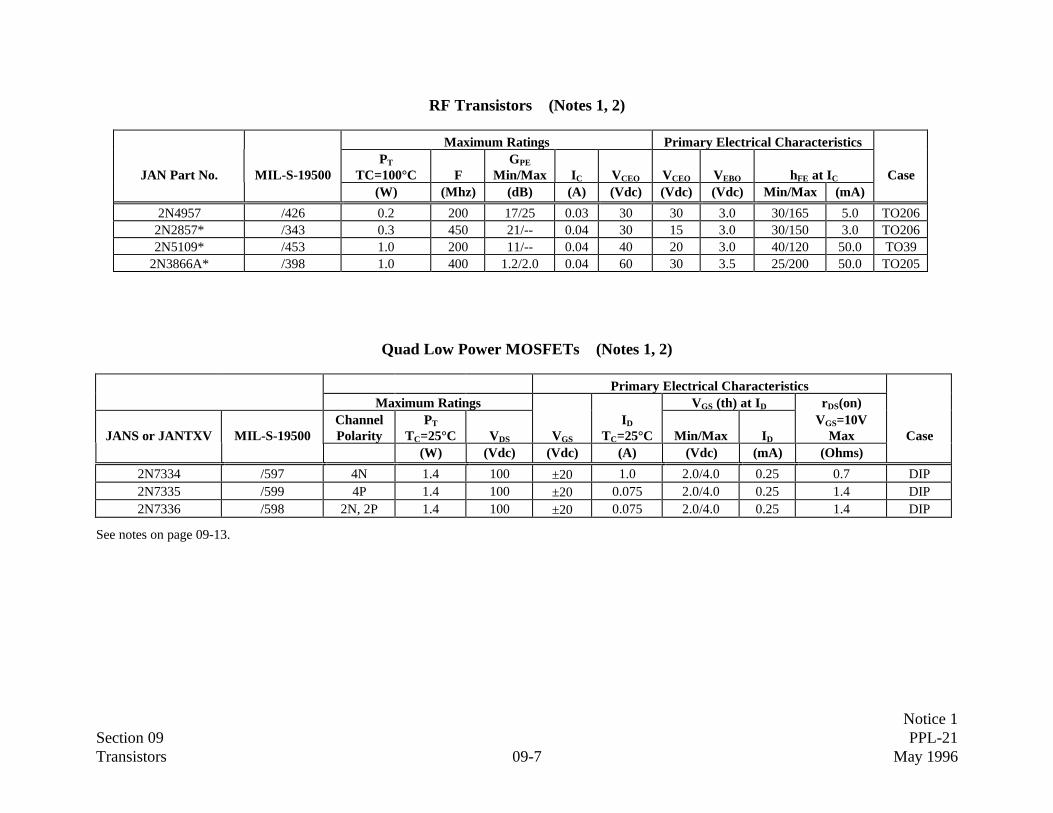
Notice 1Section 09 PPL-21Transistors 09-7 May 1996
RF Transistors (Notes 1, 2)
Maximum Ratings Primary Electrical Characteristics
JAN Part No. MIL-S-19500PT
TC=100°C FGPE
Min/Max IC VCEO VCEO VEBO hFE at IC Case(W) (Mhz) (dB) (A) (Vdc) (Vdc) (Vdc) Min/Max (mA)
2N4957 /426 0.2 200 17/25 0.03 30 30 3.0 30/165 5.0 TO2062N2857* /343 0.3 450 21/-- 0.04 30 15 3.0 30/150 3.0 TO2062N5109* /453 1.0 200 11/-- 0.04 40 20 3.0 40/120 50.0 TO39
2N3866A* /398 1.0 400 1.2/2.0 0.04 60 30 3.5 25/200 50.0 TO205
Quad Low Power MOSFETs (Notes 1, 2)
Primary Electrical CharacteristicsMaximum Ratings VGS (th) at ID rDS(on)
JANS or JANTXV MIL-S-19500ChannelPolarity
PT
TC=25°C VDS VGS
ID
TC=25°C Min/Max ID
VGS=10VMax Case
(W) (Vdc) (Vdc) (A) (Vdc) (mA) (Ohms)
2N7334 /597 4N 1.4 100 ±20 1.0 2.0/4.0 0.25 0.7 DIP2N7335 /599 4P 1.4 100 ±20 0.075 2.0/4.0 0.25 1.4 DIP2N7336 /598 2N, 2P 1.4 100 ±20 0.075 2.0/4.0 0.25 1.4 DIP
See notes on page 09-13.

Notice 1Section 09 PPL-21Transistors 09-8 May 1996
N-Channel Power MOSFETs (Notes 1, 2) (Page 1 of 2)
Maximum Ratings Primary Electrical CharacteristicsVGS(th) at ID RDS(on) gfs
JAN Part No. MIL-S-19500PT
TC= 25°CVDS VGS ID
TC= 25°CMin/Max ID VGS=10V
MaxMin Max Case
(W) (Vdc) (Vdc) (A) (Vdc) (mA) (Ohm) (mhos)
2N6660 /547 6.25 60 ±20 0.99 0.8/2 1.0 3.0 TO392N6661 /547 6.25 90 ±20 0.86 0.8/2 1.0 4.0 TO392N6901 /570 8.33 100 ±10 1.69 1/2 1.0 1.4 0.3 12.0 TO392N6903 /570 8.33 200 ±20 0.98 1/2 1.0 3.65 0.05 2.0 TO392N6782 /556 15 100 ±10 3.50 2/4 0.25 0.6 1.0 3.0 TO392N6784 /556 15 200 ±20 2.25 2/4 0.25 1.5 0.9 2.7 TO392N6786 /556 15 400 ±20 1.25 2/4 0.25 3.6 0.7 2.1 TO392N6788 /555 20 100 ±20 6.0 2/4 0.25 0.30 1.5 4.5 TO392N6790 /555 20 200 ±20 3.5 2/4 0.25 0.80 1.5 4.5 TO392N6792 /555 20 400 ±20 2.0 2/4 0.25 1.80 1.0 3.0 TO392N6794 /555 20 500 ±20 1.5 2/4 0.25 3.00 1.0 3.0 TO392N6796 /557 25 100 ±20 8.0 2/4 0.25 0.18 3.0 4.0 TO392N6798 /557 25 200 ±20 5.5 2/4 0.25 0.4 2.5 7.5 TO392N6800 /557 25 400 ±20 3.0 2/4 0.25 1.0 2.0 6.0 TO392N6802 /557 25 500 ±20 2.5 2/4 0.25 1.5 1.5 4.5 TO392N6756 /542 75 100 ±20 14.0 2/4 0.25 0.18 4.0 12.0 TO32N6758 /542 75 200 ±20 9.0 2/4 0.25 0.4 3.0 9.0 TO32N6760 /542 75 400 ±20 5.5 2/4 0.25 1.0 3.0 9.0 TO32N6762 /542 75 500 ±20 4.5 2/4 0.25 1.5 2.5 7.5 TO32N6902 /566 75 100 ±10 12 1/2 1.0 0.20 0.3 12.0 TO32N6904 /566 75 200 ±10 8.0 1/2 1.0 0.65 0.3 12.0 TO3
2N7218U* /596 125 100 ±20 28.0 2/4 0.25 0.077 TO2542N7219U* /596 125 200 ±20 18.0 2/4 0.25 0.18 TO2542N7221U* /596 125 400 ±20 10.0 2/4 0.25 0.55 TO2542N7222U* /596 125 500 ±20 8.0 2/4 0.25 0.85 TO254
See notes on page 09-13.

Notice 1Section 09 PPL-21Transistors 09-9 May 1996
N-Channel Power MOSFETs (Notes 1, 2) (Page 2 of 2)
Maximum Ratings Primary Electrical CharacteristicsVGS(th) at ID RDS(on) gfs
JAN Part No. MIL-S-19500PT
TC= 25°CVDS VGS ID
TC= 25°CMin/Max ID VGS=10V
MaxMin Max Case
(W) (Vdc) (Vdc) (A) (Vdc) (mA) (Ohms) (mhos)
2N6764 /543 150 100 ±20 38.0 2/4 0.25 0.055 9.0 27.0 TO32N6766 /543 150 200 ±20 30.0 2/4 0.25 0.085 9.0 27.0 TO32N6768 /543 150 400 ±20 14.0 2/4 0.25 0.300 8.0 24.0 TO32N6770 /543 150 500 ±20 12.0 2/4 0.25 0.400 8.0 24.0 TO3
2N7224U* (Note 3) /592 150 100 ±20 34.0 2/4 0.25 0.070 TO2542N7225 /592 150 200 ±20 27.0 2/4 0.25 0.10 TO2542N7227 /592 150 400 ±20 14.0 2/4 0.25 0.315 TO254
2N7228U* (Note 3) /592 150 500 ±20 12.0 2/4 0.25 0.415 TO2542N7236* /595 125 200 ±20 18.0 2/4 0.25 0.20 TO2542N7237* /595 125 200 ±20 11.0 2/4 0.25 0.51 TO2542N7334 /597 1.4 500 ±20 1.0 2/4 0.25 0.70 M0Q362N7335 /599 1.4 500 ±20 0.75 2/4 0.25 1.4 M0Q362N7336 /598 1.4 500 ±20 1.0 2/4 0.25 0.7 M0Q36
R2N7261* /601 25 100 ±20 8.0 2/4 0.25 0.18 2.5 TO205H2N7262 /601 25 200 ±20 5.5 2/4 0.25 0.4 2.5 TO205
G2N7268* /603 150 100 ±20 34.0 2/4 0.25 0.065 8.0 TO254R2N7269* /603 150 200 ±20 26.0 2/4 0.25 0.100 8.0 TO254
See notes on page 09-13.

Notice 1Section 09 PPL-21Transistors 09-10 May 1996
P-Channel Power MOSFETs (Notes 1, 2)
Maximum Ratings Primary Electrical Characteristics
JAN Part No. MIL-S-19500PT
TC= 25°C VDS VGS
ID
TC= 25°C VGS(th) at ID
rDS(on)VGS=10V gfs Case
Min/Max ID Max Min Max(W) (Vdc) (Vdc) (A) (Vdc) (mA) (Ohms) (mhos)
2N6895 /565 8.33 100 ±20 1.16 2/4 1.0 3.65 0.2 0.8 TO392N6845 /563 20 100 ±20 4.0 2/4 0.25 0.6 1.25 3.75 TO392N6847 /563 20 200 ±20 2.5 2/4 0.25 1.5 1.0 3.0 TO392N6849* /564 25 100 ±20 6.5 2/4 0.25 0.30 2.5 7.5 TO392N6851 /564 25 200 ±20 4.0 2/4 0.25 0.80 2.2 6.6 TO392N6896 /565 60 100 ±20 6.0 2/4 1.0 0.60 1.0 4.0 TO32N6804 /562 75 100 ±20 11.0 2/4 0.25 0.30 3.0 9.0 TO32N6806* /562 75 200 ±20 6.5 2/4 0.25 0.8 2.0 6.0 TO32N6897* /565 100 100 ±20 12 2/4 1.0 0.35 2.0 8.0 TO32N7236* /595 125 200 ±20 18.0 2/4 0.25 0.20 TO2542N7236U* (Note 3) /595 125 100 ±20 18 2/4 0.25 0.20 TO2542N7237* /595 125 200 ±20 11.0 2/4 0.25 0.51 TO2542N7237U* (Note 3) /595 125 200 ±20 11 2/4 0.25 0.51 TO2542N6898 /565 150 100 ±20 25 2/4 1.0 0.20 4.0 1.6 TO3
PNP Darlington Transistors (Notes 1, 2)
Maximum Ratings Primary ElectricalCharacteristics
PT hFE at IC
JAN Part No. MIL-S-19500 TC=100°C IC VCBO VCEO VEBO Min/Max VCE(sat) at IC Case
(W) (A) (Vdc)
(Vdc) (Vdc) (x 1000) (A) (Vdc) (A)
2N6299 /540 32 8 80 80 5 0.75/18 4 2.0 4 TO662N6649 /527 85 10 60 60 5 1/20 5 2.0 5 TO32N6650 /527 85 10 80 80 5 1/20 5 2.0 5 TO3
See notes on page 09-13.

Notice 1Section 09 PPL-21Transistors 09-11 May 1996
NPN Darlington Transistors (Notes 1, 2)
Maximum Ratings Primary ElectricalCharacteristics
PT hFE at IC
JAN Part No. MIL-S-19500 TC=100°C IC VCBO VCEO VEBO Min/Max VCE(sat) at IC Case(W) (A) (Vdc) (Vdc) (Vdc) (x 1000) (A) (Vdc) (A)
2N6350 /472 5 5 80 80 12 2/10 5 1.5 5 TO332N6351 /472 5 5 150 150 12 1/10 5 2.5 5 TO332N6352 /472 25 5 80 80 12 2/10 5 1.5 5 TO662N6353 /472 25 5 150 150 12 1/10 5 2.5 5 TO662N6301 /539 32 8 80 80 5 0.75/18 4 2.0 4 TO662N6384 /523 100 10 60 60 5 1/20 5 2.0 5 TO32N6385 /523 100 10 80 80 5 1/20 5 2.0 5 TO32N6283 /504 175 20 80 80 7 1.25/18 10 3.0 20 TO32N6284 /504 175 20 100 100 7 1.25/18 10 3.0 20 TO3
N-Channel FETs (Notes 1, 2)
Maximum Ratings Primary Electrical CharacteristicsPT VGS(OFF) IDSS
JAN Part No. MIL-S-19500 TA=25°°C VDG VDS VGS IG Min Max tON tOFF Min/Max Ciss Case(mW) (Vdc) (Vdc) (Vdc) (mA) (Vdc) (Vdc) (ns) (ns) (mA) (pF)
2N5545 /430 400 50 50 30 0.5 4.5 0.5/8.0 6 TO712N5546 /430 400 50 50 30 0.5 4.5 0.5/8.0 6 TO712N5547 /430 400 50 50 30 0.5 4.5 0.5/8.0 6 TO71
2N3821* /375 300 50 50 10 4 0.5/2.5 6 TO722N3822* /375 300 50 50 50 10 6 2/10 6 TO722N3823 /375 300 30 30 30 10 8 4/20 6 TO722N4856 /385 360 40 40 40 50 4 10 6 25 50/175 18 TO182N4857 /385 360 40 40 40 50 2 6 6 50 20/100 18 TO182N4858 /385 360 40 40 40 50 .8 4 10 100 8/80 18 TO182N4859 /385 360 30 30 50 50 4 10 6 25 50/175 18 TO182N4860 /385 360 30 30 50 50 2 6 6 50 20/100 18 TO182N4861 /385 360 30 30 50 50 0.8 4 10 100 8/80 18 TO18
See notes on page 09-13.

Notice 1Section 09 PPL-21Transistors 09-12 May 1996
P-Channel FETs (Notes 1, 2)
Maximum Ratings Primary Electrical CharacteristicsPT VGS(OFF) IDSS
JAN Part No. MIL-S-19500 TA=25°C VDG VDS VGS IG IGSS Min Max tON TOF
F
Min/Max Ciss Case
(mW) (Vdc) (Vdc) (Vdc) (mA) (nA) (Vdc) (Vdc) (ns) (ns) (mA) (pF)
2N5114 /476 500 30 30 30 50 1000 5 10 6 6 30/90 25 TO182N5115 /476 500 30 30 30 50 1000 3 6 10 8 15/60 25 TO182N5116 /476 500 30 30 30 50 1000 1 4 25 20 5/25 27 TO18
Silicon Dual Transistors, Complementary (Notes 1, 2)
Maximum Ratings Primary Electrical Characteristics
JAN Part No. MIL-S-19500PT
Each SideTA=25°C
IC VCB VCE VBE hFE at IC VCE(sat) at IC C Case
(mW) (mA) (Vdc) (Vdc) (Vdc) Min/Max (mA) (Vdc) (mA) (pF)
2N4854U /421 300/600 600 60 40 5 100/300 150 0.4 150 300 (Note 3)
See notes on page 09-13.

Notice 1Section 09 PPL-21Transistors 09-13 May 1996
Optocouplers (Notes 1, 2)
LED Section PhotoTransistorJAN Part No. MIL-S-19500 IF IP VF at IF VCEO VCBO VEBO VCE (SAT)
at IC tr and tf Case(mA) (A) (Vdc) (mA) (Vdc) (Vdc) (Vdc) (Vdc) (mA) (µs)
4N22 /486 40 1 1.3 10 35 35 4 0.3 2.54N23 /486 40 1 1.3 10 35 35 4 0.3 5.04N24 /486 40 1 1.3 10 35 35 4 0.3 10.04N47* /548 40 1 1.5 10 40 45 7 0.3 2.0 20 TO-994N48* /548 40 1 1.5 10 40 45 7 0.3 2.0 20 TO-994N49* /548 40 1 1.5 10 40 45 7 0.3 2.0 25 TO-99
Notes:1. An asterisk (*) next to the device number indicates that the part is available to both JANS and JANTXV assurance levels. The absence of the asterisk
indicates that the part is available only to the JANTXV assurance level. All JANS transistors are preferred Grade 1 parts.2. All JANTXV transistors must be PIND tested in accordance with Appendix A and are preferred Grade 2 parts.3. For transistors which are available in leaded and unleaded (U designation) configurations, the leaded package (case) is designated. Refer to the detail
specification for surface mount (unleaded) package outlines.

Notice 1Section 09 PPL-21Transistors 09-14 May 1996
THIS PAGE INTENTIONALLY LEFT BLANK

Section 10 PPL-21Microcircuits 10-1 March 1995
Summary of Preferred Microcircuits
Description Refer to Page No.
MIL-M-38510 Part Number Explanation 10-2
MIL-I-38535 Part Number Explanation 10-2
Low Power Schottky: 54LS Series 10-3
Advanced Low Power Schottky: 54ALS Series 10-5
Digital CMOS: 4000B Series 10-5
Advanced Schottky: 54F Series 10-6
CMOS High Speed: 54HC/HCT Series 10-7
Advanced CMOS Technology: 54AC/ACT Series 10-8
BIPOLAR and MOS Memories 10-9
MOS Microprocessors and Interface Peripherals 10-9
Semi-Custom Bipolar Array Logic 10-10
Application-Specific-Integrated Circuits (ASIC) and Masked Gate Arrays 10-11
Linear Bipolar and Bi-FETs 10-12
Linear CMOS 10-14
Summary of Preferred Hybrid Microcircuits 10-15

Section 10 PPL-21Microcircuits 10-2 March 1995
MIL-M-38510 Part Number Explanation (Note 1)
Part Number Explanation:M38510 /or M, D, R, H XXX XX X X X
Military Designator Radiation Hardness Detailed Specification Device Type Device Class Case Outline Lead FinishAssurance (RHA)
Designator Establishes detail Determines the S = Grade 1 Defines package A - Hot solder diprequirements and specific circuit. B = Grade 2 type. B - Tin Platespecific electrical C - Gold Plate
characteristics of themicrocircuits.
MIL-I-38535 SMD One-Part-One Part Number Explanation (Note 1)
Part Number Explanation:5962 /or M, D, R, H XXXXX XX X X X
Military Designator Radiation Hardness Drawing Designator Device Type Device Class Case Outline Lead FinishAssuranceDesignator Establishes detail Determines the V = Grade 1 Defines package A - Hot solder dip
requirements and specific circuit. Q = Grade 2 type. B - Tin Platespecific electrical C - Gold Plate
characteristics of themicrocircuits.
See notes on page 10-19.
M = 3 x 10³ RAD (Si)D = 1 x 10⁴ RAD (Si)R = 1 x 10⁵ RAD (Si)H = 1 x 10⁶ RAD (Si)
M = 3 x 10³ RAD (Si)D = 1 x 10⁴ RAD (Si)R = 1 x 10⁵ RAD (Si)H = 1 x 10⁶ RAD (Si)

Section 10 PPL-21Microcircuits 10-3 March 1995
Low Power Schottky: 54LS Series (Notes 2, 3) (Page 1 of 2)
See notes on page 10-19.
GenericNumber MIL-M-38510
CircuitDescription
Gates54LS00 /30001* QUAD 2-INPUT, NAND54LS03 /30002* QUAD 2-IN, NAND, OPEN COLLECTOR54LS04 /30003* HEX INVERTER54LS05 /30004* HEX INVERTER OPEN-COLLECTOR O/P54LS10 /30005* TRIPLE 3-INPUT NAND54LS20 /30007* DUAL 4-INPUT NAND54LS22 /30008 4-INPUT OPEN COLLECTOR NAND54LS02 /30301 QUAD 2-INPUT NOR54LS27 /30302 TRIPLE 3-INPUT NOR54LS51 /30401 DUAL 2-WIDE AND-OR-INVERTER54LS32 /30501 QUAD 2-INPUT OR54LS86 /30502* QUAD 2-INPUT X-OR54LS08 /31004 QUAD 2-INPUT AND54LS09 /31005 2-INPUT, OPEN COLLECTOR AND54LS11 /31001* TRIPLE 3-INPUT AND54LS21 /31003* DUAL 4-INPUT AND54LS26 /32102 2-INPUT OPEN COLLECTOR. NAND
Buffers/Drivers54LS365 /32201 HEX, COMMON ENABLE, 3-STATE54LS366 /32202 HEX, INV, COMMON ENABLE, 3-STATE54LS367 /32203 HEX, 4-BIT/2-BIT, NONINV, 3-STATE54LS368 /32204 HEX, 4-BIT/2-BIT, INVERTING., 3-STATE54LS125A /32301 QUAD , NONINV 3- STATE54LS126 /32302 QUAD , NONINV 3- STATE54LS240 /32401 OCTAL , INVERTER, 3- STATE
54LS245 /32803 OCTAL, BUS TRANSCEIVER, 3-STATE
GenericNumber MIL-M-38510
CircuitDescription
Buffers/Drivers54LS241 /32402 OCTAL , NONINV , 3- STATE OUTPUTS54LS244 /32403* OCTAL , NONINV , 3- STATE OUTPUTS54LS365 /32201 HEX , NONINV , 3-STATE OUTPUTS54LS366 /32202 HEX , INVERTER , 3-STATE OUTPUTS54LS367 /32203 HEX , NONINV , 3-STATE OUTPUTS54LS38 /30203 QUAD, 2-INPUT NAND OPEN-COLL.54LS541 /32405 OCTAL , NONINV , 3-STATE OUTPUTS
Latches54LS75 /31601 D-TYPE , 4-BIT BISTABLE54LS279 /31602 RS, QUAD54LS259 /31603 D-TYPE , OCTAL , ADDRESSABLE54LS377 /32504 D-TYPE , OCTAL54LS373 /32502 D-TYPE , OCTAL, TRANSPARENT
Flip-Flops54LS74A /30102 D-TYPE , DUAL54LS112 /30103 JK , DUAL WITH RESET/CLEAR, NEG.54LS113 /30104 JK , DUAL WITH RESET/ CLEAR54LS174 /30106 D-TYPE , HEX54LS175 /30107 D-TYPE, QUAD54LS109 /30109 JK , DUAL WITH RESET/CLEAR, POS.54LS76A /30110 JK , DUAL , NEGATIVE EDG-TRIG54LS273 /32501 D-TYPE , OCTAL WITH CLEAR54LS374 /32503 D-TYPE , OCTAL , 3-STATE OUTPUTS54LS123 /31401 MONOSTABLE, DUAL , RETRIG.54LS221 /31402 MONOSTABLE, DUAL , RETRIG.54LS173A /36101 D-TYPE , QUAD

Section 10 PPL-21Microcircuits 10-4 March 1995
Low Power Schottky: 54LS Series (Notes 2, 3) (Page 2 of 2)
See notes on page 10-19.
GenericNumber MIL-M-38510
CircuitDescription
Combinational Gates54LS138 /30701* 3-LINE-TO-8-LINE DECODER54LS139 /30702 DUAL 2-LINE-TO-4-LINE DECODER54LS42 /30703* BCD-TO-7-SEGMENT DECODER54LS151 /30901 8-IN PUT DATA SELECT/MULTIPLEXER54LS153 /30902* DUAL 4-INPUT DATA SELECT/MUX54LS157 /30903* QUAD 2-INPUT DATA SELECT/MUXER54LS158 /30904* QUAD 2-INPUT INV. OUTPUTS MUX54LS251 /30905* 8-BIT 3-STATE, DATA SELECT/MUX54LS257B /30906 2-INPUT 3- STATE DATA SELECT/MUX54LS258B /30907 2-INPUT 3- STATE DATA SELECT/MUX54LS253 /30908* 4-INPUT 3- STATE DATA SELECT/MUX54LS85 /31101 4-BIT MAGNITUDE COMPARATOR54LS83A /31201 4-BIT FULL ADDER, FAST CARRY54LS283 /31202 4-BIT FULL ADDER , FAST CARRY54LS280 /32901 9-BIT PARITY GENERATOR/CHECKER54LS148 /36001 8-LINE-TO-3-LINE PRIORITY
ENCODER54LS348 /36002 8-TO-3-LINE PRIORITY ENCODER
GenericNumber MIL-M-38510
CircuitDescription
Shift Registers54LS194A /30601* 4- BIT BIDIRECTIONAL54LS195A /30602 4- BIT PARALLEL ACCESS54LS95B /30603 4-BIT PARALLELEL ACCESS54LS96 /30604 5-BIT SHIFT REGISTER54LS164 /30605* 8-BIT PARALLEL-OUT, SERIAL-IN54LS295B /30606 4-BIT BIDIRECTIONAL54LS395A /30607 4-BIT UNIVERSAL54LS165A /30608 8-BIT PARALLEL-IN, SERIAL-OUT54LS166 /30609 8-BIT PARALLEL-IN, SERIAL-OUT54LS670 /31901 4 X 4 , 3-STATE OUTPUTS REGISTER FILE
Counters54LS90 /31501 4-BIT DECADE54LS93 /31502 4-BIT DECADE54LS160A /31503 4-BIT SYNC DECADE54LS161 /31504 4-BIT SYNC BINARY, ASYNC RESET54LS193 /31508 4-BIT SYNC BIN UP/DOWN54LS191 /31509 4-BIT SYNC BIN UP/DOWN54LS92 /31510 DIVIDE-BY-1254LS163A /31512 4-BIT SYNC BINARY, SYNC RESET54LS197 /32002 PRESET 50/30 MHZ BINARY54LS290 /32003 4-BIT DECADE54LS293 /32004 4-BIT BINARY54LS390 /32701 DUAL 4-BIT A&B I/P DECADE54LS393 /32702 DUAL 4-BIT BINARY

Section 10 PPL-21Microcircuits 10-5 March 1995
Advanced Low Power Schottky: 54ALS Series Digital CMOS: 4000B Series (Notes 2, 3)
See notes on page 10-19.
GenericNumber MIL-M-
38510
CircuitDescription
Gates/Combinational Gates54ALS00A /37001 QUAD 2-INPUT NAND54ALS10 /37002 TRIPLE 3-INPUT NAND54ALS20A /37003 DUAL 4-INPUT NAND54ALS30A /37004 8-INPUT NAND54AL133 /37005 13-INPUT NAND54ALS04B /37006 HEX INVERTER54ALS02 /37301 QUAD 2-INPUT NOR54ALS27 /37302 TRIPLE 3-INPUT NOR54ALS08 /37401 QUAD 2-INPUT AND54ALS11 /37402 TRIPLE 3-INPUT AND54ALS32 /37501 QUAD 2-INPUT OR54ALS1000A /38401 QUAD 2-INPUT NAND54ALS1002 /38402 QUAD 2-INPUT NOR54ALS1020 /38407 DUAL 4-INPUT NAND54ALS138 /37701 3-TO-8-LINE DECODER/DEMUX
Buffers/Drivers54ALS1034 /38411 HEX , NONINV BUFFER/DRIVER54ALS240A /38301 OCTAL , BUFFER, INV, , 3-STATE OUTPUT54ALS241 /38302 OCTAL , BUFFER, NONINV, 3-STATE OUTPUT54ALS244B /38303 OCTAL , BUFFER, NONINV, 3-STATE OUTPUT
Flip-Flops54ALS109A /37102 JK , DUAL , PRESET(ACTIVE HIGH)54ALS112A /37103 JK , DUAL , PRESET(ACTIVE LOW)54ALS174 /37201 D-TYPE , HEX , WITH CLEAR54ALS175 /37202 D-TYPE , QUAD , WITH CLEAR54ALS373 /37203 D-TYPE , OCTAL , 3-STATE OUTPUTS54ALS374 /37204 D-TYPE , OCTAL , EDGE-TRIGGER54ALS573 /38201 D-TYPE ,OCTAL , 3--STATE OUTPUTS54ALS574A /37104 D-TYPE , OCTAL54ALS74A /37101 D-TYPE, DUAL -POSITIVE TRIGGER
Counters54ALS161B /38001 4-BIT SYNC, BINARY54ALS163B /38002 4-BIT SYNC, CLEAR BINARY54ALS169B /38003 4-BIT SYNC, UP/DOWN BINARY
GenericNumber MIL-M-38510
CircuitDescription
Gates/Combinational Gates4001B H05252* QUAD, 2-INPUT NOR4002B H05253* DUAL, 4-INPUT NOR4025B H05254* TRIPLE, 3-INPUT NOR4011B H05051* QUAD, 2-INPUT NAND4012B H05052* DUAL, 4-INPUT NAND4023B H05053* TRIPLE, 3-INPUT NAND4007UB H05351* DUAL, COMPLEMENTARY PAIR, INVERTER4019B H05352* QUAD, AND-OR SELECT4070B H17203* QUAD, 2-INPUT X-OR4071B H17101* QUAD, 2-INPUT OR4072B H17102* DUAL, 4-INPUT OR4075B H17103* TRIPLE, 3-INPUT OR4081B H17001* QUAD, 2-INPUT AND4082B R17002 DUAL, 4-INPUT AND4073B R17003 TRIPLE, 3-INPUT AND4077B R17204 QUAD, 2-INPUT X-NOR4085B H17201* DUAL, AND-OR-INVERT, 2-WIDE, 2-INPUT4086B H17202* DUAL, AND-OR-INVERT, 4-WIDE, 2-INPUT4049UB H05553* HEX BUFFER, INVERTING4050B H05554* HEX BUFFER4041UB R05555 QUAD, TRUE COMPLEMENT BUFFER4069UB H17401* HEX INVERTER4502B R17403* HEX INVERTER/BUFFER4028B R05951* BCD-TO-DECIMAL DECODER4066B H05852* QUAD, BILATERAL SWITCH
Flip-Flops4098B R17504 MONOSTABL MULTIVIBRATOR, DUAL4099B R17601 D-TYPE , OCTAL LATCH,4013B H05151* D-TYPE, DUAL, EDGE-TRIGGERED4027B H05152* JK, DUAL
Sequential Registers/Counters4008B R05451* 4-BIT FULL ADDER4017B H05651* DECADE COUNTER/DIVIDER4020B H05653* BIN COUNT ER, 14-STAGE CARRY4022B H05654* OCTAL COUNTER W/8 DECODED OUTPUT4024B H05655* 7-STAGE RIPPLE CARRY COUNT/DIVIDE4014B H05752* 8-BIT SERIAL/PARALLEL REGISTER4015B H05753* DUAL, SERIAL IN, PARALLEL OUT4021B H05754* 8-BIT ASYNC PARALLEL IN/SERIAL OUT

Section 10 PPL-21Microcircuits 10-6 March 1995
Advanced Schottky: 54F Series (Notes 2, 3)
See notes on page 10-19.
GenericNumber MIL-M-38510
CircuitDescription
Gates54F00 /33001* QUAD, 2-INPUT NAND54F04 /33002* HEX, INVERTER54F10 /33003* TRIPLE, 3-INPUT NAND54F20 /33004* DUAL, 4-INPUT NAND54F02 /33301* QUAD, 2-INPUT NOR54F64 /33401* 4-2-3-2 INPUT AND-/OR-INVERTER54F08 /34001* QUAD, 2-INPUT AND54F11 /34002* QUAD, 2-INPUT AND54F32 /33501* QUAD, 2-INPUT OR54F86 /34501* QUAD, 2-INPUT EXCLUSIVE-OR
Buffers/Drivers54F240 /33201 OCTAL, INV, 3-STATE OUTPUTS54F241 /33202* OCTAL, NONINV, 3-STATE OUTPUTS54F244 /33203* OCTAL, NONINV, 3-STATE OUTPUTS54F245 /34803* OCTAL, NONINV, BUS TRANSCEIVER54F365 /35101 HEX , NONINV, 3-STATE OUTPUTS
Flip-Flops54F074 /34101* D-TYPE, DUAL54F109 /34102 JK , DUAL54F175 /34104 D-TYPE, QUAD54F374 /34105 D-TYPE, OCTAL 3-STATE OUTPUTS54F534 /34106 D-TYPE, OCTAL 3-STATE OUTPUTS54F174 /34107* D-TYPE, HEX54F373 /34601* D-TYPE, OCTAL , 3-STATE OUTPUTS54F533 /34602 D-TYPE ,OCTAL 3-STATE OUTPUTS54F563 /34603 D-TYPE , OCTAL ,3-STATE OUTPUTS54F573 /34604 D-TYPE , OCTAL 3-STATE OUTPUTS
GenericNumber MIL-M-38510
CircuitDescription
Combinational Gates54F138 /33701* 3-TO-8-LINE DECODER54F139 /33702* DUAL, 2-LINE-TO-4-LINE DECODER54F151A /33901* 8-INPUT DATA SELECT, MULTIPLEXER54F153 /33902* DUAL, 4-INPUT DATA SELECT, MUX54F157A /33903* QUAD, 2-INPUT DATA SELECT, MUX54F158A /33904* QUAD, 2-INPUT DATA SELECT, MUX54F181 /33801 4-BIT ALU GENERATOR54F182 /33802 LOOK AHEAD CARRY GENERATOR54F251A /33905* 8-INPUT , 3-STATE OUTPUTS, MUX54F253 /33908* DUAL, 4-INPUT, 3-STATE OUTPUTS, MUX54F257A /33906* QUAD, 2-INPUT , 3-STATE OUTPUTS, MUX54F258A /33907* QUAD, 2-INPUT , 3-STATE OUTPUTS, MUX54F280 /34901* 9-BIT PARITY GENERATOR/CHECKER54F283 /34201* 4-BIT FULL ADDER54F521 /34701* 8-BIT IDENTITY COMPARATOR54F398 /35001* QUAD , 2-INPUT WITH STORAGE MUX
Counters/Shift Registers54F160A /34401* 4-BIT SYNC BCD DECADE COUNTER54F161A /34301* 4-BIT SYNC BINARY COUNTER54F163A /34302* 4-BIT SYNC BINARY COUNTER54F192 /34404 4-BIT SYNC UP/DOWN DECADE COUNTER54F193 /34304 4-BIT SYNC UP/DOWN BINARY COUNTER54F194 /33601* 4-BIT BIDIRECT. UNIVERSAL SHIFT
REGISTER

Section 10 PPL-21Microcircuits 10-7 March 1995
CMOS High-Speed: 54HC/HCT Series (Notes 2, 3)
See notes on page 10-19.
GenericNumber MIL-M-38510
CircuitDescription
Gates54HC00 /65001 QUAD, 2-INPUT NAND54HC10 /65002 TRIPLE, 3-INPUT NAND54HC20 /65003 DUAL, 4-INPUT NAND54HC30 /65004 8-INPUT NAND54HC02 /65101 QUAD, 2-INPUT NOR54HC27 /65102 TRIPLE, 3-INPUT NOR54HC266 /65103 QUAD, 2- INPUT EXCLUSIVE- NOR54HC4002 /65104 DUAL, 4-INPUT NOR54HCT04 /65751 HEX, INVERTER (TTL)54HC04 /65701 HEX, INVERTER54HC14 /65702 SCHMITCH- TRIGGER HEX INVERTER54HC08 /65203 QUAD, 2-INPUT AND54HC11 /65204 TRIPLE, 3-INPUT AND54HC32 /65201 QUAD, 2-INPUT OR54HC86 /65202 QUAD, 2-INPUT X-OR
Buffers/Drivers54HC245 /65503 OCTAL, XSCEIVER, NONINV., 3-STATE54HCT245 /65553 OCTAL, XSCEIVER, NONINV., 3-ST (TTL)54HCT240 /65753 OCTAL, INV. WITH 3-STATE OUTPUTS54HC240 /65703 OCTAL, INV. WITH 3- STATE OUTPUTS54HC365 /65706 HEX, NONINV WITH 3- STATE OUTPUTS54HC367 /65708 HEX, NONINV WITH 3- STATE OUTPUTS54HC368 /65709 HEX, INV, WITH 3- STATE OUTPUTS54HC540 /65710 OCTAL, INV, 3- STATE OUTPUTS54HC541 /65711 OCTAL, NONINV, WITH 3-STATE OUTPUTS54HCT244 /65755 OCTAL, NONINV, 3-STATE OUTPUTS (TTL)
GenericNumber MIL-M-38510
CircuitDescription
Flip-Flops54HC74 /65302 D-TYPE , DUAL , WITH PRESET AND CLEAR54HC109 /65304 JK, DUAL54HC112 /65305 JK, DUAL WITH R/S54HC173 /65306 D-TYPE, QUAD WITH 3-STATE OUTPUTS54HC174 /65307 D-TYPE, HEX WITH CLEAR54HC175 /65308 D-TYPE, QUAD54HCT74 /65352 D-TYPE, DUAL R/C (TTL)54HC273 /65601 D-TYPE, OCTAL WITH CLEAR54HC574 /65604 D-TYPE, OCTAL WITH 3-STATE OUTPUTS54HCT374 /65652 D-TYPE, OCTAL (TTL), NON-INVERTING
Latches54HC259 /65402 D-TYPE, OCTAL ADDRESSABLE54HC373 /65403 D-TYPE, OCTAL WITH 3-STATE OUTPUTS54HC573 /65406 D-TYPE, OCTAL WITH 3-STATE OUTPUTS54HCT373 /65453 D-TYPE, OCTAL (TTL), TRANSPARENT
Combinational Gates54HCT138 /65852 3-LINE-TO-8-LINE DECODER (TTL)54HC138 /65802 3-LINE-TO-8-LINE DECODER54HC139 /65803 DUAL, 2 TO 4 LINE DECODER
Counters54HC161 /66302 4-BIT BINARY COUNTER, ASYNC RESET54HC163 /66304 4-BIT BINARY COUNTER, SYNC RESET54HC393 /66309 DUAL, 4-BIT BINARY COUNTER

Section 10 PPL-21Microcircuits 10-8 March 1995
Advanced CMOS Technology: 54AC/ACT Series (Notes 2, 3)
See notes on page 10-19.
GenericNumber MIL-M-38510
CircuitDescription
Gates54AC00 R75001* QUAD, 2-INPUT NAND54AC10 R75002* TRIPLE, 3-INPUT NAND54AC20 R75003* DUAL, 4-INPUT NAND54AC02 R75101* QUAD, 2-INPUT NOR54AC04 R75701* HEX INVERTER54AC14 R75702* SCHMITT TRIGGER, HEX INVERTER54AC08 R75203* QUAD, 2-INPUT AND54AC11 R75204* TRIPLE, 3-INPUT AND54AC32 R75201* QUAD, 2-INPUT OR54AC86 R75202* QUAD, 2-INPUT X-OR
Buffers/Drivers54AC240 R75703 OCTAL, INV, 3- STATE OUTPUTS54AC241 R75704* OCTAL, NONIN, 3- STATE OUTPUTS54AC244 R75705* OCTAL, NONINV, 3- STATE OUTPUTS54AC245 R75503* OCTAL, BUS TRANSCEIVER ,
BIDIRECTIONAL, 3-STATE OUTPUTS
GenericNumber MIL-M-38510
CircuitDescription
Combinational Gates54AC138 R75802* 3-LINE-TO-8-LINE DECODER/DEMUX54AC139 R75803* DUAL, 2-TO-4 DECODER/ DEMUX54AC151 /76201* 8-INPUT MULTIPLEXER54AC153 /76202* DUAL, 4-INPUT MULITIPLEXER54AC157 /76203* QUAD, 2-INPUT MULTIPLEXER
Shift Registers54AC299 /76506* 8-BIT UNIVERSAL PARALLEL
Flip-Flops54AC273 /75601* D-TYPE , OCTAL WITH CLEAR54AC377 /75603* D-TYPE, OCTAL, CLOCK ENABLE54AC373 R75403* D-TYPE , OCTAL, 3-STATE OUTPUTS54AC74 /75302* D-TYPE, DUAL, POSITIVE EDGE- TRIGGER54AC574 /75604* D-TYPE, OCTAL, 3-STATE OUTPUTS54AC374 /75606* D-TYPE , OCTAL, 3-STATE OUTPUTS54AC109 /75304* JK, DUAL, POSITIVE EDGE-TRIGGER
GenericNumber 5962
CircuitDescription
Comparators54AC520 -90916* 8-BIT MAGNITUDE COMPARATOR, PULL-
UP RESISTOR54AC521 R90985* 8-BIT MAGNITUDE COMPARATOR
Gates54ACT00 R8769901* QUAD 2-INPUT NAND
Buffers/Drivers54ACT240 R8775901 OCTAL, INV, 3- STATE OUTPUTS54ACT244 R8776001* OCTAL, NON-INV, 3- STATE OUTPUTS54ACT245 R8766301* OCTAL, BIDIRECTIONAL XCEIVER,
3-STATECombinational Gates
54ACT138 -8755401* 3-LINE-TO-8-LINE DECODER54ACT151 -8875601* 8-INPUT MULTIPLEXER
Flip-Flops54ACT377 -8769701* D-TYPE, OCTAL, CLOCK ENABLE54ACT74 -8752501* D-TYPE, DUAL, POSITIVE EDGE-TRIGGER54ACT574 -8960101* D-TYPE, OCTAL, 3-STATE OUTPUTS

Section 10 PPL-21Microcircuits 10-9 March 1995
Bipolar and MOS Memories (Notes 2,3) MOS Microprocessors and Interface Peripherals
See notes on page 10-19.
GenericNumber MIL-M-
38510
Circuit DescriptionSize Access Time
Bipolar PROMs82S185 /20902 2K X 4, 125 NS, 3-STATE OUTPUT82S191 /21002 2K X 8, 125 NS, 3-STATE OUTPUTMOS SRAMs2147 /28903 4K X 1 , 55 NS , 3-STATE OUTPUT2148 /28904 1K X 4 , 55 NS, 3-STATE OUTPUT2147 /28901 4K X 1, 35 NS2148 /28902 1K X 4, 35 NS2147 /23801 4K X 1 , 85 NS, 3-STATE OUTPUT2147H /23803 4K X 1,70 NS2147H-3 /23805 4K X 1, 55 NS2148 /23806 1K X 4, 70 NS2147H-2 /23807 4 K X 1, 45 NS6504 /24501 4K X 1 , 300 NS6514 /24502 1K X 4 , 300 NS6116 /29104 2K X 8 , 90 NS6516 /29102 2K X 8 , 200 NS65162 /29110 2K X 8 , 70 NS65262 /29103 16K X 1 , 85 NS65262 /29109 16K X 1 , 150 NS, 3-STATE OUTPUT65642 /29205 8K X 8 , 150 NS
GenericNumber 5962
CircuitDescription
Microprocessor/MicrocontrollerMQ80386Q20 -8766803 32 BIT, 20 MHZ MICROPROCESSORQM80386Q25 -8766804 32 BIT, 25 MHZ MICROPROCESSORMQ80387Q-XX -89534XX 80 BIT NUMERIC PROCESSORLORFXPC H9202601* FIXED POINT PROCESSORLORFLPC H9210301* FLOATING POINT PROCESSOR
LORAP1C H9210401* ADDRESS PROCESSOR ONE
LORAP2C H9210601* ADDRESS PROCESSOR TWO
GenericNumber 5962
Circuit DescriptionSize Access Time
SRAMs(Note 3) H3829437* 8K X 8 , 55 NS, RAD-HARD
" H3829436* 8K X 8 , 70 NS, RAD-HARD" H3829435* 8K X 8 , 85 NS, RAD-HARD" H9215305* 32 K X 8, 60 NS, RAD-HARD" H9215307* 32 K X 8, 40 NS, RAD-HARD" H9312802* 256 K X 1, 60 NS, RAD-HARD" H9312803* 256 K X 1, 40 NS, RAD-HARD
GenericNumber MIL-M-38510
CircuitDescription
Bus InterfacesUT1553BRTI /55501 MIL-STD-1553 RT INTERFACE
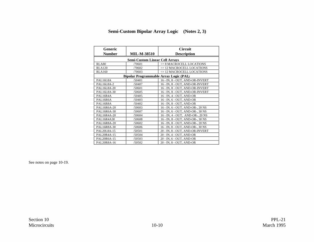
Section 10 PPL-21Microcircuits 10-10 March 1995
Semi-Custom Bipolar Array Logic (Notes 2, 3)
See notes on page 10-19.
GenericNumber MIL-M-38510
CircuitDescription
Semi-Custom Linear Cell ArraysRLA80 /70601 <= 8 MACROCELL LOCATIONSRLA120 /70602 <= 12 MACROCELL LOCATIONSRLA160 /70603 <= 12 MACROCELL LOCATIONS
Bipolar Programmable Array Logic (PAL)PAL16L8A /50401 16 - IN, 8 - OUT, AND-OR-INVERTPAL16L8A-2 /50407 16 - IN, 8 - OUT, AND-OR-INVERTPAL16L8A-20 /50601 16 - IN, 8 - OUT, AND-OR-INVERTPAL16L8A-30 /50605 16 - IN, 8 - OUT, AND-OR-INVERTPAL16R4A /50405 16 - IN, 4 - OUT, AND-ORPAL16R6A /50403 16 - IN, 6 - OUT, AND-ORPAL16R8A /50402 16 - IN, 8 - OUT, AND-ORPAL16R6A-20 /50603 16 - IN, 6 - OUT, AND-OR-, 20 NSPAL16R6A-30 /50607 16 - IN, 6 - OUT, AND-OR-, 30 NSPAL16R4A-20 /50604 16 - IN, 4 - OUT, AND-OR-, 20 NSPAL16R4A30 /50608 16 - IN, 8 - OUT, AND-OR-, 30 NSPAL16R8A-20 /50602 16 - IN, 8 - OUT, AND-OR-, 20 NSPAL16R8A-30 /50606 16 - IN, 8 - OUT, AND-OR-, 30 NSPAL20L8A-15 /50501 20 - IN, 8 - OUT, AND-OR-INVERTPAL20R4A-15 /50504 20 - IN, 4 - OUT, AND-ORPAL20R6A-15 /50503 20 - IN, 6 - OUT, AND-ORPAL20R8A-16 /50502 20 - IN, 8 - OUT, AND-OR

Section 10 PPL-21Microcircuits 10-11 March 1995
Application-Specific-Integrated-Circuits (ASIC) and Masked Gate Arrays (Note 4)
Manufacturer Process Technology RHA Grade Circuit Description
UTMC 1.2 µm DLM CMOS1.5 µm DLM CMOS1.2 µm TLM CMOS
HHH
1, 21, 2 25,000 - 105,000 Gates
Honeywell 1.2 µm RICMOS III0.8 µm RICMOS IV
HH
1, 21, 2
10,000 - 340,000 Gates
Loral 1.0 µm RHCMOS1.0 µm RHCMOS-E0.5 µm HMCMOS
HHH
1, 21, 21, 2
50,000 - 300,000 Gates
AMI 1.25 µm DLM CMOS N/A 2 10,000-300,000 Gates
See notes on page 10-19.

Section 10 PPL-21Microcircuits 10-12 March 1995
Linear Bipolar and Bi-FETs (Notes 2, 3) (Page 1 of 2)
See notes on page 10-19.
GenericNumber MIL-M-38510
CircuitDescription
Operational Amplifiers101A108A118741A, 148
/10103*/10104*/10107*/10101*
SINGLE, EXT. COMPENSATEDSINGLE, EXT. COMPENSATEDPRECISION, HIGH SPEEDSINGLE, INT. COMPENSATED
L558LH2108A747ALH2101A
/10108*/10106/10102*/10105
DUAL, INT. COMPENSATEDDUAL, EXT. COMPENSATEDDUAL, INT. COMPENSATEDDUAL, HIGH PERFORMANCE
41364156, 4741124, 2101A124A148
/11004*/11003/11005/11006*/11001*
QUADQUADQUAD, LOW POWERQUAD, SINGLE SUPPLYQUAD, MEDIUM POWER
155155A156A156157157A
/11401*/11404*/11405*/11402*/11403/11406
JFET INPUT, LOW POWERJFET INPUT, LOW POWERJFET INPUT, HIGH PERFORM.JFET INPUT, LOW POWERJFET INPUT, LOW POWERJFET INPUT, HIGH PERFORM.
25002510252026002620
/12204/12205/12206/12202/12203
SINGLE, HIGH PRECISION/ SLEWSINGLE, HIGH PRECISION/ SLEWSINGLE, HIGH SLEWSINGLE, WIDEBANDSINGLE HIGH SPEED, WIDEBAND
OP-07OP-27AOP-07A
/13502*/13503*/13501*
LOW OFFSETPRECISIONULTRA LOW OFFSET
LF411M, 071LF153, 072LF1 47, 074
/11904/11905/11906
BI-FET, LOW POWERBI-FET, LOW POWER, DUALBI-FET, LOW POWER, QUAD
5532A5534A
/13102/13101
LOW NOISE, DUALLOW NOISE
GenericNumber MIL-M-38510
CircuitDescription
Transmission Line Receivers/Drivers55107A5510855114 961455115, 9615
/10401/10402/10403/10404
LINE RECEIVER, DUAL DIFFERENTIALLINE RECEIVER, DUAL DIFFERENTIALLINE RECEIVER, DUAL DIFFERENTIALLINE RECEIVER, DUAL DIFFERENTIAL
5511355114
/10405/10403
LINE DRIVER, DUAL DIFFERENTIALLINE DRIVER, DUAL DIFFERENTIAL
5545155452554545546255463
/12902/12903/12905/12908/12909
PERIPHERAL DRIVER, DUAL ANDPERIPHERAL DRIVER, DUAL NANDPERIPHERAL DRIVER, DUAL NORPERIPHERAL DRIVER, DUAL NANDPERIPHERAL DRIVER, DUAL OR
Comparators111119119A2111711710
/10304*/10306*/10307*/10305*/10302/10301
VOLTAGE COMPARATOR/ BUFFER DUAL,SINGLE HIGH SPEEDDUAL, HIGH SPEEDDUAL, PRECISION COMPARATORDUAL, HIGH SPEEDSINGLE, HIGH SPEED
139193
/11201*/11202
QUAD, SINGLE SUPPLY, LOW POWERDUAL, LOW POWER/OFFSETTimers
555556
/10901*/10902
TIMER, PRECISIONDUAL, PRECISION

Section 10 PPL-21Microcircuits 10-13 March 1995
Linear Bipolar and Bi-FET Devices (Notes 2, 3) (Page 2 of 2)
See notes on page 10-19.
GenericNumber MIL-M-38510
CircuitDescription
Voltage Regulators109140LAH-05,78M05140LAH-12,78M12140LAH-15, 78M1540AAK-05, 7805140AK-12,7812140AK-15, 7815140AK-24, 7824
/10701*/10702/10703/10704/10706/10707/10708/10709
5V FIXED POSITIVE, 1.5A5V FIXED POSITIVE, 0.5A12V FIXED POSITIVE, 0.5A15V FIXED POSITIVE, 0.5A5V FIXED POSITIVE, 1.0A12V FIXED POSITIVE, 1.0A15V FIXED POSITIVE, 1.0A24V FIXED POSITIVE, 1.0A
120H-05, 79M05120H-12, 79M12120H-15, 79M15120K-05, 7905120K-12, 7912120K-15, 7915120K24, 7924
/11501*/11502*/11503*/11505*/11506*/11507*/11508
5V FIXED NEGATIVE, 0.5A12V FIXED NEGATIVE, 0.5A15V FIXED NEGATIVE, 0.5A12V FIXED NEGATIVE, 0.5A5V FIXED NEGATIVE, 1.0A15V FIXED NEGATIVE, 1.0A24V FIXED NEGATIVE,1.0A
137H137K
/11803*/11804*
ADJUSTABLE NEGATIVE, 0.5AADJUSTABLE NEGATIVE, 1.5A
117H117K138K
/11703*/11704*/11706
ADJUSTABLE POSITIVE, 0.5AADJUSTABLE POSITIVE, 1.5AADJUSTABLE POSITIVE
LT1009AD584SAD584T
/14802*/12801/12802
PROGRAMMABLE V REF.PROGRAMMABLE V REFPROGRAMMABLE V REF.
1524, 18461525A15261527A
/12601/12602/12603/12604
PULSE WIDTH MODULATOR,REGULATING
GenericNumber MIL-M-38510
CircuitDescription
Transistor Arrays2001200220032004200528012802280328042805
/14101/14102/14103/14104/14105/14106/14107/14108/14109/14110
DARLINGTON TRANSISTORS
D/A ConvertersDAC08SDAC08SAAD562AD565AD561
/11301*/11302*/12101/12103/13301
8-BIT, HIGH SPEED MULTIPLYING8-BIT, HIGH SPEED MULTIPLYING12-BIT, CURRENT OUTPUT12-BIT, CURRENT OUTPUT10-BIT, CURRENT OUTPUT
A/D Converters574AU574AT
/14001/14002
12-BIT, 35 µS12-BIT
S/H Amplifiers198 /12501* SAMPLE AND HOLD AMPLIFIER
MultipliersAD534TAD534SAD532S
/13901/13902/13903
4-QUADRANT, 1% ERROR, 1MHZ BW4-QUADRANT, 1% ERROR, 1MHZ BW4-QUADRANT, 4% ERROR, 1MHZ BW

Section 10 PPL-21Microcircuits 10-14 March 1995
Linear CMOS (Notes 2, 3)
See notes on page 10-19.
GenericNumber MIL-M-38510/
CircuitDescription
Analog Switches181A182A184A185A187A188A190A191A
/11101/11102/11103/11104/11105/11106/11107/11108
SPST, 2- CHANNELSPST, 2- CHANNELDPST, 2- CHANNEL_DPST, 2- CHANNELSPSTSPDTSPDT, 2- CHANNELSPDT, 2- CHANNEL
200201
/12301/12302
SPST, 2-CHANNELSPST, 4- CHANNEL
300301302303304305306307
/11601/11602/11603/11604/11605/11606/11607/11608
SPST, 2-CHANNELSPDT, 1-CHANNELDPST, 2-CHANNELSPDT, 2-CHANNELSPST, 2-CHANNELSPDT, 2-CHANNELDPST, 2-CHANNELSPDT, 2-CHANNEL
504050415042504350445045
/10501/10502/10503/10504/10505/10506
SPST, 1-CHANNELSPST, 2-CHANNELSPDT, 1-CHANNELSPDT, 2-CHANNELDPST, 1-CHANNELDPST, 2-CHANNEL
GenericNumber MIL-M-38510/
CircuitDescription
Analog Multiplexers/ Demultiplexers (MUX/DEMUX)506506A507507A508508A509509A
/19001/19002/19003/19004/19007/19005/19008/19006
MUX, 16 -CHANNELMUX/DEMUX, 16-CHANNELMUX, DIFFERENTIAL 8-CHANNELMUX/DEMUX, 8-CHANNELMUX/DEMUX, 8-CHANNELMUX/DEMUX, 8-CHANNELMUX/DEMUX, , 4-CHANNELMUX/DEMUX, DIFF. 4-CHANNEL

Section 10 PPL-21Microcircuits 10-15 March 1995
Summary of Preferred Hybrid Microcircuits
Description Refer to Page No.
MIL-H-38534 SMD One-Part-One Part Number Explanation 10-16
SMD Non-One-Part-One Part Number Explanation 10-16
MIL-STD-1553 Peripherals/Controller Bus Interfaces 10-17
Optocouplers 10-17
A/D and D/A Converters 10-17
Voltage References and Regulators 10-18
DC/DC Converters 10-18
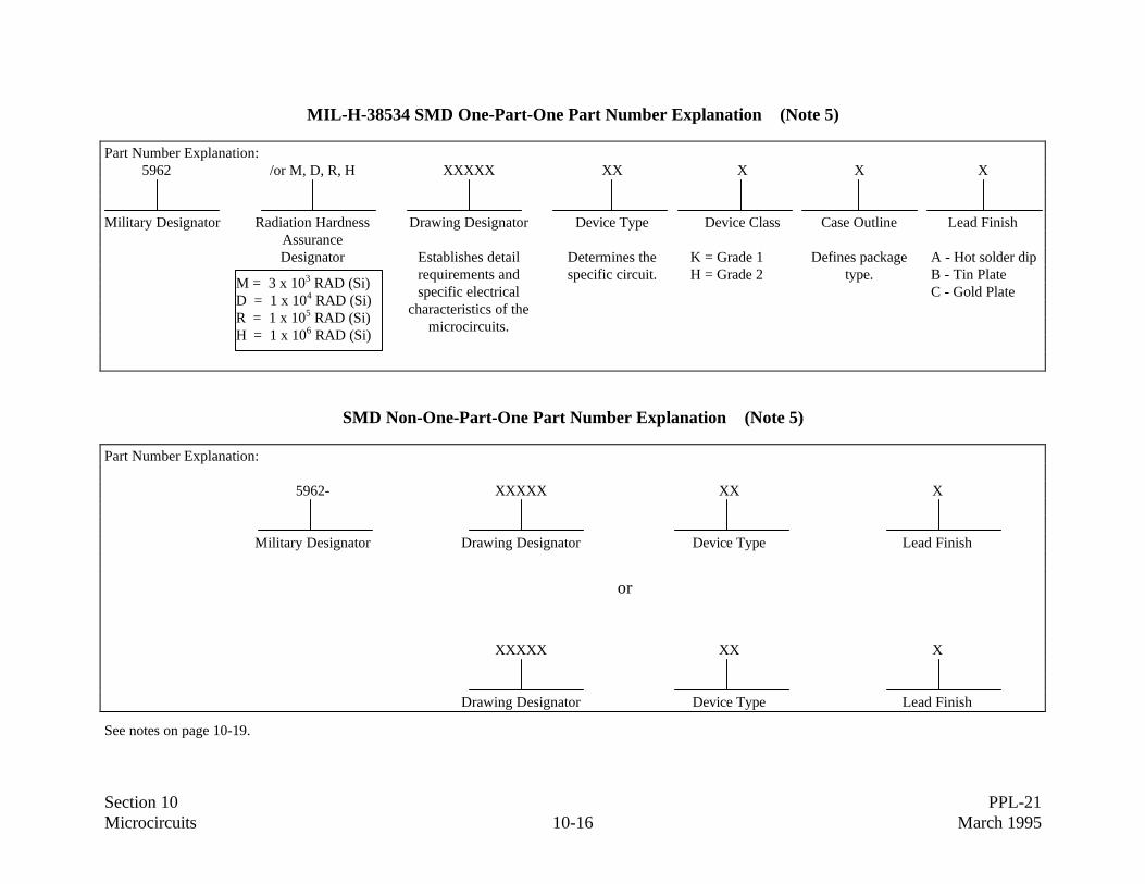
Section 10 PPL-21Microcircuits 10-16 March 1995
MIL-H-38534 SMD One-Part-One Part Number Explanation (Note 5)
Part Number Explanation:5962 /or M, D, R, H XXXXX XX X X X
Military Designator Radiation Hardness Drawing Designator Device Type Device Class Case Outline Lead FinishAssuranceDesignator Establishes detail Determines the K = Grade 1 Defines package A - Hot solder dip
requirements and specific circuit. H = Grade 2 type. B - Tin Platespecific electrical C - Gold Plate
characteristics of themicrocircuits.
SMD Non-One-Part-One Part Number Explanation (Note 5)
Part Number Explanation:
5962- XXXXX XX X
Military Designator Drawing Designator Device Type Lead Finish
or
XXXXX XX X
Drawing Designator Device Type Lead Finish
See notes on page 10-19.
M = 3 x 10³ RAD (Si)D = 1 x 10⁴ RAD (Si)R = 1 x 10⁵ RAD (Si)H = 1 x 10⁶ RAD (Si)

Section 10 PPL-21Microcircuits 10-17 March 1995
Hybrid Microcircuits (Note 5) (Page 1 of 2)
See notes on page 10-19.
GenericNumber
5962 orSMD No.
CircuitDescription
MIL-STD-1553 Peripherals/Controller Bus Interfaces(NOTE 3) -88692XX BC/RTU/MT, MUX TERMINAL(NOTE 3) -91734XX BC/RTU/MT, MUX TERMINAL(NOTE 3) -87535XX DUAL REDUNDANT RTU(NOTE 3) -91786XX DUAL REDUNDANT RTU(NOTE 3) -89798XX DUAL REDUNDANT RTU(NOTE 3) -87579XX DRIVER/RECEIVER, DUAL CHANNEL(NOTE 3) -89447XX DRIVER/RECEIVER, DUAL CHANNEL(NOTE 3) -89522XX DRIVER/RECEIVER, DUAL CHANNEL(NOTE 3) -89826XX DRIVER/RECEIVER, DUAL CHANNEL(NOTE 3) -92061XX DRIVER/RECEIVER, DUAL CHANNEL(NOTE 3) -86049XX DRIVER/RECEIVER, SINGLE CHANNEL(NOTE 3) -91749XX DRIVER/RECEIVER, SINGLE CHANNEL(NOTE 3) -92085XX DRIVER/RECEIVER, SINGLE CHANNEL(NOTE 3) -88586XX BUS TO µPROCESSOR INTERFACE(NOTE 3) -92162XX BUS INTERFACE, RTU, DUAL
(NOTE 3) -93065XX MUX TERMINAL W/ 4K RAM
OptocouplersHCPL-5761 -8947701 AC/DC TO LOGIC INTERFACE
4N55 -8767901 2-CHANNEL
(NOTE 3) 8102801 2-CHANNELHCPL-5231 -8876902 2-CHANNEL
HCPL-1931 -89572XX 2-CHANNEL
HCPL-5531 -8767902 2-CHANNEL, COMMON SUPPLY
HCPL5431 -8957101 2-CHANNEL, COMMON SUPPLY
(NOTE 3) -8978501 2-CHANNEL, COMMON SUPPLY
HCPL-6531 -8767903 2-CHANNEL, SEPARATE SUPPLY
(NOTE 3) -8978502 2-CHANNEL, SEPARATE SUPPLY
HCPL-6231 -8876901 2-CHANNEL, SEPARATE SUPPLY
HSSR-7111 -9314001 1-CHANNEL, POWER MOSFET
(NOTE 3) -8981001 1-CHANNEL, HIGH GAIN
HCPL-5201 -8876801 1-CHANNEL
66079 -9167601 1-CHANNEL
HCPL5401 -8957001 1-CHANNEL, HIGH SPEED
HCPL5601 -9085501 1-CHANNEL, HIGH SPEED
(NOTE 3) -9085401 1-CHANNEL,TRANSISTOR OUTPUT
GenericNumber
5962 orSMD No.
CircuitDescription
A/D Converters(NOTE 3) -88508XX A/D, 12-BITAD9005ATM -9066601 A/D, 12-BITCLC925B8C -9099501 A/D, 12-BITMN5200-5206 -89583XX A/D, 12-BITAD578 -89658XX A/D, 12-BIT,HIGH-SPEEDMN5210-5215 -89584XX A/D, 12-BIT, HIGH-SPEEDADC00302 -88542XX A/D, 12-BIT, TRACK/HOLDMN5246 -89595XX A/D, 12-BIT, ± 2.5VSP9588 -9063101 A/D, 14-BITMN5295 -8956901 A/D, 16-BITMN5290/5291 -8956301 A/D, 16-BITMN6400 -9177001 A/D, 16-BITMN6450 -9225301 A/D, 16-BITAD1385 -9171201 A/D, 16-BITHS9576 -90795XX A/D, 16-BIT, ± 0.003 %FSRHS1068 -8877601 A/D, 8-BIT FLASHSP1078 -8997901 A/D, 8-BIT FLASHMN5143 -90497XX A/D, 8-BIT, 0 TO +10V INPUT RANGEMN5100/5101 -92073XX A/D, 8-BIT FLASHMN5142/ 5141 -90497XX A/D, 8-BIT, ± 10V
D/A ConvertersADH030 -9063401 D/A, 12-BITDAC HKB -8952801 D/A, 12-BIT, BINARY INPUT CODEMN3860 -9057001 D/A, 12-BIT, INPUT REGISTERDAC02310 -88517XX D/A, 12-BIT, DEGLITCHED(NOTE 3) -89531XX D/A, 16-BIT, 0 TO 10VHS9378 -89862XX D/A, 16-BITMN3009/3008 -8768801 D/A, 8-BIT, ± 2V OUTPUTRGBDAC3808 -89509XX D/A, 8-BIT, TRIPLEHS/MN 3020 -89718XX D/A, 8 -BIT, WITH INPUT REGISTERAD390 -88509XX D/A, 12-BIT, QUADAD394 -88510XX D/A, 12-BIT, QUADHS9342 -88629XX D/A, 12-BIT, QUAD

Section 10 PPL-21Microcircuits 10-18 March 1995
Hybrid Microcircuits (Note 5) (Page 2 of 2)
See notes on page 10-19.
GenericNumber
5962 orSMD No.
CircuitDescription
Voltage References and Regulators(NOTE 3) -93134XX VOLT. REGULATOROM7501-7509 -89490XX VOLT. REGULATOR FIXED, DUAL VOLT OUT
DC/DC ConvertersMHF-2805S -9213901 12W, 5V SINGLE OUTPUTMHF-2812S -9166401 15W, 12V SINGLE OUTPUTMHF-2852S -9160101 15W, 15V SINGLE OUTPUTMHF-2812D -9214401 15W, ±12V DUAL OUTPUTMHF-2815D -9161401 15W, ±15V DUAL OUTPUTMTR-2805S -9306801 25W, 5V SINGLE OUTPUTMTR-2805D -9320501 25W, ±5V DUAL OUTPUTMTR-2812S -9306901 30W, 12V SINGLE OUTPUTMTR-2815S -9307001 30W, 15V SINGLE OUTPUTMTR-2818S -9320201 30W, 18V SINGLE OUTPUTMTR-2812D -9307101 30W, ±12V DUAL OUTPUTMTR-2815D -9307201 30W, ±15V DUAL OUTPUTMFL-2805S -9316301 50W, 5V SINGLE OUTPUTMFL-2805D -9319101 50W, ±5V DUAL OUTPUTMSA-2815S -9309401 5W, 15V SINGLE OUTPUTMSA-2815D -9309001 5W, ±15V DUAL OUTPUTMFL-2812S -9316201 60W, 12V SINGLE OUTPUTMFL-2815S -9316101 60W, 15V SINGLE OUTPUTMSA-2812D -9308901 5W, ±12V DUAL OUTPUTMFL-2812D -9319201 60W, ±12V DUAL OUTPUTMFL-2815D -9319301 60W, ±15V DUAL OUTPUTMSA-2812S -9309301 5W, 12V SINGLE OUTPUTMSA-2805S -9309201 5W, 5V SINGLE OUTPUT

Section 10 PPL-21Microcircuits 10-19 March 1995
Notes for Preferred Microcircuits and Hybrids
Notes:1. Preferred microcircuits may be purchased to MIL-M-38510 detailed specifications or MIL-I-38535 one-part-one-part number Standard Military Drawings
(SMDs). M38510 Class S and SMD Class V microcircuits are considered preferred Grade 1 parts, and M38510 Class B and SMD Class Q microcircuits,with the addition of PIND testing in accordance with Appendix A, are considered preferred Grade 2 parts. MIL-M-38510 has been incorporated into MIL-I-38535 as Appendix A and all future microcircuit specifications will be written as SMDs (one-part-one part number).
2. An asterisk (*) next to SMD number indicates that parts are available in both classes V/S/K and Q/B/H. The absence of the asterisk indicates that partsare available only as class Q/B/H.
3. No generic number is applicable to these parts, since different manufacturers have different part ID numbers. Refer to or QML-38535, or QML-38534 forthe manufacturer's listed part number.
4. The customer controls the design details by defining the application-specific requirements completely within the Altered Item Drawing (AID). The AIDdoes not need to specify the quality and reliability requirements, as these are covered under the QML-38535 SMD certification and qualificationrequirements; however, the AID needs to supplement the requirements for specific design and fault coverage measurements in accordance with Method5012 of MIL-STD-883.
5. Preferred hybrid microcircuits are usually purchased to MIL-H-38534 One-Part-One-Part Number Standard Military Drawings (SMDs). Class K hybridswould normally be considered Grade 1 parts, but none are currently listed as preferred parts. Class H hybrids are listed and, with the addition of PINDtesting, in accordance with Appendix A, are considered preferred Grade 2 parts. These can be purchased to either MIL-H-38534 SMDs using the one-part-one-part number designation, or to older SMDs which use the non-one-part-one number designation.

Section 10 PPL-21Microcircuits 10-20 March 1995
THIS PAGE INTENTIONALLY LEFT BLANK

Notice 1Section 14 PPL-21Thermistors 14-1 May 1996
Summary of Preferred Thermistors
Style Description SpecificationResistance Range at +25°C
(ohms) Grades Refer ToMinimum Maximum
311P18 Negative Temperature Coefficient,Insulated and Uninsulated GSFC S-311-P-18 2252 3000 1, 2 Page 14-2
RTH Positive Temperature Coefficient,Insulated MIL-R-23648/19
(Note 1)10 10000 1, 2 Page 14-3
Notes:1. Effective with Revision D, dated 4 April 1995, MIL-R-23648 superseded MIL-T-23648C. The associated detail specifications were also changed from
MIL-T-23648/XX to MIL-R-23648/XX on the same date.

Notice 1Section 14 PPL-21Thermistors 14-2 May 1996
GSFC S-311-P-18 Thermistors, Insulated and Uninsulated, Nonhermetic (Note 1)
Part Number Explanation:311P18 -XX X XXX
GSFC Prefix Dash numbercorresponds tothe zero-powerresistance ofthe thermistor@ 25°C
Lead Material Type:S = 32AWG tinned solid copper wire, LW(0.20)C-51-N per MIL-STD-1276N = 32AWG solid nickel wire, LW(0.20)N-01-N per MIL-STD-1276A = 28AWG silver coated stranded wire, ETFE per M22759/33-28-9T = 28AWG silver coated stranded wire, PTFE per M16878/6BCB9E = 32AWG tinned solid copper wire, LW(0.20)C-51-N per MIL-STD-1276, one lead
bare, one lead insulated with PTFE tubing per MIL-I-22129, covered withheat shrinkable FEP insulation per M23053/11-105-C
Lead Length (cm)(Note 2)
Grade 1 and 2Part Numbers
ControlSpecification
TemperatureCoefficient
ZeroPower
Resistance(at +25°°C)
ToleranceLimits
(0 to +70°°C)
Operatingand Storage
TemperatureLimits
ResistanceRatio
ThermalTime
Constant(maximum)
DissipationConstant
(minimum)(Ohms) (+%R) (°°C) (R25°°C/Rmin) (sec) (mW/°°C)
311P18-01XXXX311P18-02XXXX
22522252
1.020.51
-55 to +90-55 to +70
10.935.71
311P18-03XXXX311P18-04XXXX
30003000
1.020.56
-55 to +90-55 to +70
10.915.71
311P18-05XXXX311P18-06XXXX
GSFC S-311-P-18 Negative 50005000
1.020.51
-55 to +90-55 to +70
10.915.71
10.0(Note 3)
1.0(Note 4)
311P18-07XXXX311P18-08XXXX
1000010000
0.930.56
-55 to +90-55 to +70
9.235.03
311P18-09XXXX311P18-10XXXX
3000030000
1.000.50
-55 to +90-55 to +70
10.725.60
Notes:1. WARNING: Use heat sinks when soldering or welding to thermistor leads.2. Standard lead lengths are from 7.6 to 100 cm. The lead length in centimeters (cm) is specified by three characters. For lengths from 7.6 to 9.9 cm, the
letter “R” is used as the decimal point (e.g., 7R6 = 7.6 cm). For lengths 10 cm to 99 cm, the letters “R” is used as the last character (e.g., 76R = 76 cm).For 100 cm lead length, the digits are 101. The first two digits represent significant figures, and the last digit specifies the number of zeros to follow.
3. For a thermistor suspended in still air, the thermal constant is 10 seconds maximum, except lead style "E”, 25 seconds maximum.4. For thermistors suspended in still air only (does not apply for lead style "E").

Notice 1Section 14 PPL-21Thermistors 14-3 May 1996
MIL-R-23648 Thermistors, Insulated, Hermetic (Note 1)
Part Number Explanation:RTHXX X X XXX X
RTH - Identifies generalpurpose thermistors.XX represents a two-digit number whichidentifies the physicalconfiguration.
Resistance RatioCharacteristic:E = 0.55 ± 10%
Lead TypeS = Solderable
Zero Power Resistance@ +25°C(Note 2)
Zero Power ResistanceTolerance @ +25°C
J = ± 5%(Note 3)
Grade 1 and 2Part Numbers
ControlSpecification Style
TemperatureCoefficient
ResistanceRatio
ResistanceValues
@ +25°C(ohms)
ThermalTime
Constant(maximum)
DissipationConstant
(minimum)
PowerRating
@ +25°C
(min) (max) (sec) (mW/°C) (watts)
RTH42ESXXXX MIL-R-23648/19 RTH42 Positive E = 0.55 ± 10% 10 10K 60 2.5 0.25
Notes:1. Parts covered by this specification contain internal connections that may reflow during installation. Heat sinking is recommended during mounting to
prevent internal solder reflow.2. The resistance is expressed in ohms and identified by a three digit number. The first two digits represent significant figures, and the last digit specifies the
number of zeros to follow. See MIL-R-23648 for a list of standard resistance values for the 10 to 100 decade.3. The specified zero power resistance tolerance is for the reference temperature (+25°C) only. See MIL-R-23648 to determine resistance tolerance changes
versus temperature and MIL-R-23648/19 for factors to determine the resistance at various temperatures.

Notice 1Section 14 PPL-21Thermistors 14-4 May 1996
THIS PAGE INTENTIONALLY LEFT BLANK
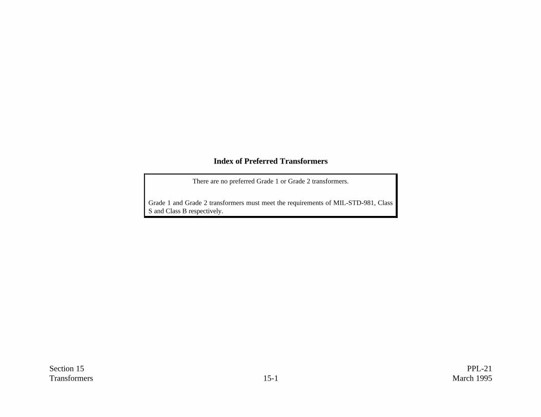
Section 15 PPL-21Transformers 15-1 March 1995
Index of Preferred Transformers
There are no preferred Grade 1 or Grade 2 transformers.
Grade 1 and Grade 2 transformers must meet the requirements of MIL-STD-981, ClassS and Class B respectively.

Section 15 PPL-21Transformers 15-2 March 1995
THIS PAGE INTENTIONALLY LEFT BLANK

Notice 1Section 16 PPL-21Wire and Cable 16-1 May 1996
Summary of Preferred Wire and Cable (Notes 1 through 3) (Page 1 of 2)
SpecificationRefer toPage No.
Insulation Selection GuidelineColor Code Designators for Wire MIL-STD-681
16-316-5
MIL-W-22759 Wire, PTFE Insulated (Polytetrafluoroethylene), Copper or Copper AlloySilver Coated, 600 Volt, 200°CNickel Coated, 600 Volt, 260°CSilver Coated, 600 Volt, 200°C (High Strength)Nickel Coated, 600 Volt, 260°C (High Strength)Silver Coated, 1000 Volt, 200°CSilver Coated, 1000 Volt, 200°C (High Strength)
MIL-W-22759/11MIL-W-22759/12MIL-W-22759/22MIL-W-22759/23MIL-W-22759/9
MIL-W-22759/20
16-616-716-716-716-716-816-8
MIL-W-22759 Wire, ETFE Insulated (Ethylene Tetrafluoroethylene), Copper or Copper AlloyTin Coated, 600 Volt, 150°C, Medium Weight InsulationTin Coated, 600 Volt, 150°C, Lightweight InsulationCrosslinked ETFE, Tin Coated, 600 Volt, 150°C, LightweightCrosslinked ETFE, Tin Coated, 600 Volt, 150°C, Normal weightCrosslinked ETFE, Silver Coated, 600 Volt, 200°C, LightweightCrosslinked ETFE, Silver Coated, 600 Volt, 200°C, Normal weightCrosslinked ETFE, Silver Coated, 600 Volt, 200°C, Lightweight (High Strength)Crosslinked ETFE, Silver Coated, 600 Volt, 200°C, Normal weight (High Strength)Crosslinked ETFE, Nickel Coated, 600 Volt, 200°C, LightweightCrosslinked ETFE, Nickel Coated, 600 Volt, 200°C, Normal weight
MIL-W-22759/16MIL-W-22759/18MIL-W-22759/32MIL-W-22759/34MIL-W-22759/44MIL-W-22759/43MIL-W-22759/33MIL-W-22759/35MIL-W-22759/45MIL-W-22759/41
16-916-9
16-1016-1116-1016-1116-1016-1116-1016-11
MIL-W-81381 Wire, FEP Fluorocarbon/Polyimide Insulated, Copper or Copper AlloySilver Coated, 600 Volt, 200°CNickel Coated, 600 Volt, 200°CTin Coated, 600 Volt, 150°CSilver Coated, 600 Volt, 200°CNickel Coated, 600 Volt, 200°C
MIL-W-81381/7MIL-W-81381/8
MIL-W-81381/21MIL-W-81381/9
MIL-W-81381/10
16-1216-1316-1316-1316-1316-13
See notes on page 16-2.

Notice 1Section 16 PPL-21Wire and Cable 16-2 May 1996
Summary of Preferred Wire and Cable (Notes 1 through 3) (Page 2 of 2)
SpecificationRefer toPage No.
S-311-P-13 Wire, High Voltage, Crosslinked Polyalkene Over Crosslinked PVDF Insulation, Copper Conductor, Tin Coated
600 Volt, 135°C1000 Volt, 135°C2500 Volt, 135°C
S-311-P-13/1S-311-P-13/2S-311-P-13/3
16-14
16-1416-1416-14
Multiconductor CableShielded and unshielded, jacketed and unjacketed MIL-C-27500 16-15
Radio Frequency Coaxial CableFlexible and Semi-Rigid MIL-C-17 16-16
J-W-1177 Magnet Wire, Copper, Enamel CoatedPolyurethane Overcoated with Polyamide, 130°CPolyester-Imide or Polyester-Amide-Imide, 180°CPolyester Overcoated with Polyamide-Imide, 200°CPolyimide-Coated, 200°C
J-W-1177/9J-W-1177/12J-W-1177/14J-W-1177/15
16-1716-1716-1716-1716-17
Notes:1. All wire and cable may be used in Grade 1 or 2 applications.2. The following are common trade names for insulations: PTFE & FEP, DuPont Teflon, ETFE and Crosslinked ETFE DuPont Tefzel, Polyvinylidene
Fluoride (PVDF, PVF2) Penwalt Kynar, Polyester DuPont Dacron, Polyimide DuPont Kapton, Polyamide DuPont Nylon.3. Wire size AWG24 and larger is preferred for conductors used in interconnecting cable and harness assemblies. High strength copper alloy shall be used
for size AWG24 and smaller.
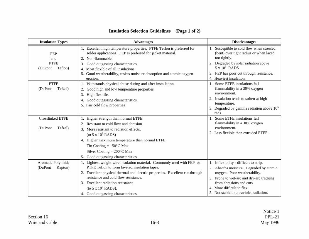
Notice 1Section 16 PPL-21Wire and Cable 16-3 May 1996
Insulation Selection Guidelines (Page 1 of 2)
Insulation Types Advantages Disadvantages
FEPand
PTFE(DuPont Teflon)
1. Excellent high temperature properties. PTFE Teflon is preferred forsolder applications. FEP is preferred for jacket material.
2. Non-flammable.3. Good outgassing characteristics.4. Most flexible of all insulations.5. Good weatherability, resists moisture absorption and atomic oxygen
erosion.
1. Susceptible to cold flow when stressed(bent) over tight radius or when lacedtoo tightly.
2. Degraded by solar radiation above5 x 105 RADS.
3. FEP has poor cut through resistance.4. Heaviest insulation.
ETFE(DuPont Tefzel)
1. Withstands physical abuse during and after installation.2. Good high and low temperature properties.3. High flex life.4. Good outgassing characteristics.5. Fair cold flow properties
1. Some ETFE insulations failflammability in a 30% oxygenenvironment.
2. Insulation tends to soften at hightemperature.
3. Degraded by gamma radiation above 106
radsCrosslinked ETFE
(DuPont Tefzel)
1. Higher strength than normal ETFE.2. Resistant to cold flow and abrasion.3. More resistant to radiation effects.
(to 5 x 10⁷ RADS)4. Higher maximum temperature than normal ETFE.
Tin Coating = 150°C MaxSilver Coating = 200°C Max
5. Good outgassing characteristics.
1. Some ETFE insulations failflammability in a 30% oxygenenvironment.
2. Less flexible than extruded ETFE.
Aromatic Polyimide(DuPont Kapton)
1. Lightest weight wire insulation material. Commonly used with FEP orPTFE Teflon to form layered insulation tapes.
2. Excellent physical thermal and electric properties. Excellent cut-throughresistance and cold flow resistance.
3. Excellent radiation resistance(to 5 x 10⁹ RADS).
4. Good outgassing characteristics.
1. Inflexibility - difficult to strip.2. Absorbs moisture. Degraded by atomic
oxygen. Poor weatherability.3. Prone to wet-arc and dry-arc tracking
from abrasions and cuts.4. More difficult to flex.5. Not stable to ultraviolet radiation.

Notice 1Section 16 PPL-21Wire and Cable 16-4 May 1996
Insulation Selection Guidelines (Page 2 of 2)
Insulation Types Advantages Disadvantages
Crosslinked Polyalkene 1. Dual extrusion which is fused by sintering. Combines excellent abrasionand cut through resistance of Polyvinylidene Fluride (PVDF, PVF2 -Penwalt Corp TM Kynar) with Polyolefin for greater flexibility andimproved heat resistance. Polyalkene is used mainly as a primaryinsulation under an outer jacket such as crosslinked ETFE or crosslinkedPVDF/PVF2.
2. High dielectric constant, used in high voltage applications.3. PVDF has good radiation resistance (to 108 RADS).4. More resistant to cold flow.5. Good outgassing characteristics.
1. Lower maximum conductor temperaturerating.(135°C for GSFC S-311-P-13)(150°C for MIL-W-81044)
2. Reduced flexibility.

Notice 1Section 16 PPL-21Wire and Cable 16-5 May 1996
Color Code Designators for Wire According to MIL-STD-681
BaseColor
1stStripe
2ndStripe Designator
BaseColor
1stStripe
2ndStripe Designator
BaseColor
1stStripe
2ndStripe Designator
BlackBrown
RedOrangeYellowGreenBlue
VioletGrayWhite
WhiteWhiteWhiteWhiteWhiteWhiteWhiteWhiteWhite
BlackBrown
RedOrangeYellowGreenBlue
VioletGray
0123456789
909192939495969798
WhiteWhiteWhiteWhiteWhiteWhiteWhiteWhite
WhiteWhiteWhiteWhiteWhiteWhiteWhite
WhiteWhiteWhiteWhiteWhiteWhite
BlackBlackBlackBlackBlackBlackBlackBlack
BrownBrownBrownBrownBrownBrownBrown
RedRedRedRedRedRed
BrownRed
OrangeYellowGreenBlue
VioletGray
RedOrangeYellowGreenBlue
VioletGray
OrangeYellowGreenBlue
VioletGray
901902903904905906907908
912913914915916917918
923924925926927928
WhiteWhiteWhiteWhiteWhite
WhiteWhiteWhiteWhite
WhiteWhiteWhite
WhiteWhite
OrangeOrangeOrangeOrangeOrange
YellowYellowYellowYellow
GreenGreenGreen
BlueBlue
YellowGreenBlue
VioletGray
GreenBlue
VioletGray
BlueVioletGray
VioletGray
934935936937938
945946947948
956957958
967968

Notice 1Section 16 PPL-21Wire and Cable 16-6 May 1996
MIL-W-22759 Wire, Fluoropolymer-Insulated, Copper or Copper Alloy (Notes 1, 2)
Part Number Explanation:
M22759 /XX -XX -XXX
Military Specification Detail Specification Wire Size Color CodeNumber (AWG) in accordance
with MIL-STD-681
Notes:
1. Flammability properties of these wires are controlled by the applicable specifications. However, applications in Space Transportation System (STS)payloads may require that the specific STS flammability hazards be addressed. Users are advised to consult the appropriate project systems safety officer.
2. Due to the cold flow phenomena of teflon insulation, the designer is advised to not route teflon insulated wires over sharp edges and tight turns, or applytight stitches and tie wraps to cable assemblies.

Notice 1Section 16 PPL-21Wire and Cable 16-7 May 1996
MIL-W-22759 Wire, Extruded PTFE (Note 1)Fluoropolymer Insulated, 600 Volt
Conductor
Coating
Max Temperature
Specification
Copper
Silver (Note 2)
200°°C
MIL-W-22759/11
Copper
Nickel
260°°C
MIL-W-22759/12
High StrengthCopper
Silver (Note 2)
200°°C
MIL-W-22759/22
High StrengthCopper
Nickel
260°°C
MIL-W-22759/23WireSize,AWG
Stranding(Number of
Strands x AWGSize of Strands)
FinishedWire
Diameter(Inches)
Part Number(Note 3)
Part Number(Note 3)
Part Number(Note 3)
Part Number(Note 3)
28262422
7 x 3619 x 3819 x 3619 x 34
0.033 ± 0.0020.038 ± 0.0020.043 ± 0.0020.049 ± 0.002
M22759/11-28-XXM22759/11-26-XXM22759/11-24-XXM22759/11-22-XX
M22759/12-28-XXM22759/12-26-XXM22759/12-24-XXM22759/12-22-XX
M22759/22-28-XXM22759/22-26-XXM22759/22-24-XXM22759/22-22-XX
M22759/23-28-XXM22759/23-26-XXM22759/23-24-XXM22759/23-22-XX
20181614
19 x 3219 x 3019 x 2919 x 27
0.058 ± 0.0020.068 ± 0.0020.075 ± 0.0020.090 ± 0.002
M22759/11-20-XXM22759/11-18-XXM22759/11-16-XXM22759/11-14-XX
M22759/12-20-XXM22759/12-18-XXM22759/12-16-XXM22759/12-14-XX
M22759/22-20-XX M22759/23-20-XX
12108
19 x 2537 x 26133 x 29
0.111 ± 0.0030.139 ± 0.0040.202 ± 0.004
M22759/11-12-XXM22759/11-10-XXM22759/11-8-XX
M22759/12-12-XXM22759/12-10-XXM22759/12-8-XX
Notes:1. Wire may be used in Grade 1 and 2 applications.2. Silver-coated copper is susceptible to cuprous oxide corrosion (“red plague”) when produced, stored or used in a moist or high humidity environment. The
environment for this wire must be controlled.3. Part number: The X in the part number column shall be replaced by color code designators in accordance with MIL-STD-681. Refer to page 16-5.
Examples: Size 20, white - M22759/9-20-9; white with orange stripe - M22759/9-20-93.

Notice 1Section 16 PPL-21Wire and Cable 16-8 May 1996
MIL-W-22759 Wire, Extruded PTFE (Note 1)Fluoropolymer Insulated, 1000 Volt
Conductor
Coating
Max Temperature
Specification
Copper
Silver (Note 2)
200°°C
MIL-W-22759/9
High Strength Copper
Silver (Note 2)
200°°C
MIL-W-22759/20WireSize,AWG
Stranding (Number ofStrands x AWG Size of
Strands)
Finished WireDiameter(Inches)
Part Number(Note 3)
Part Number(Note 3)
28262422
7 x 3619 x 3819 x 3619 x 34
0.043 ± 0.0020.048 ± 0.0020.053 ± 0.0020.060 ± 0.002
M22759/9-28-XXM22759/9-26-XXM22759/9-24-XXM22759/9-22-XX
M22759/20-28-XXM22759/20-26-XXM22759/20-24-XXM22759/20-22-XX
20181614
19 x 3219 x 3019 x 2919 x 27
0.068 ± 0.0020.078 ± 0.0020.085 ± 0.0020.100 ± 0.003
M22759/9-20-XXM22759/9-18-XXM22759/9-16-XXM22759/9-14-XX
M22759/20-20-XX
12108
19 x 2537 x 26133 x 29
0.120 ± 0.0040.141 ± 0.0040.207± 0.003
M22759/9-12-XXM22759/9-10-XXM22759/9-8-XX
Notes:1. Wire may be used in Grade 1 and 2 applications.2. Silver-coated copper is susceptible to cuprous oxide corrosion (“red plague”) when produced, stored or used in a moist or high humidity environment. The
environment for this wire must be controlled.3. Part number: The X in the part number column shall be replaced by color code designators in accordance with MIL-STD-681. Refer to page 16-5.
Examples: Size 20, white - M22759/9-20-9; white with orange stripe - M22759/9-20-93.
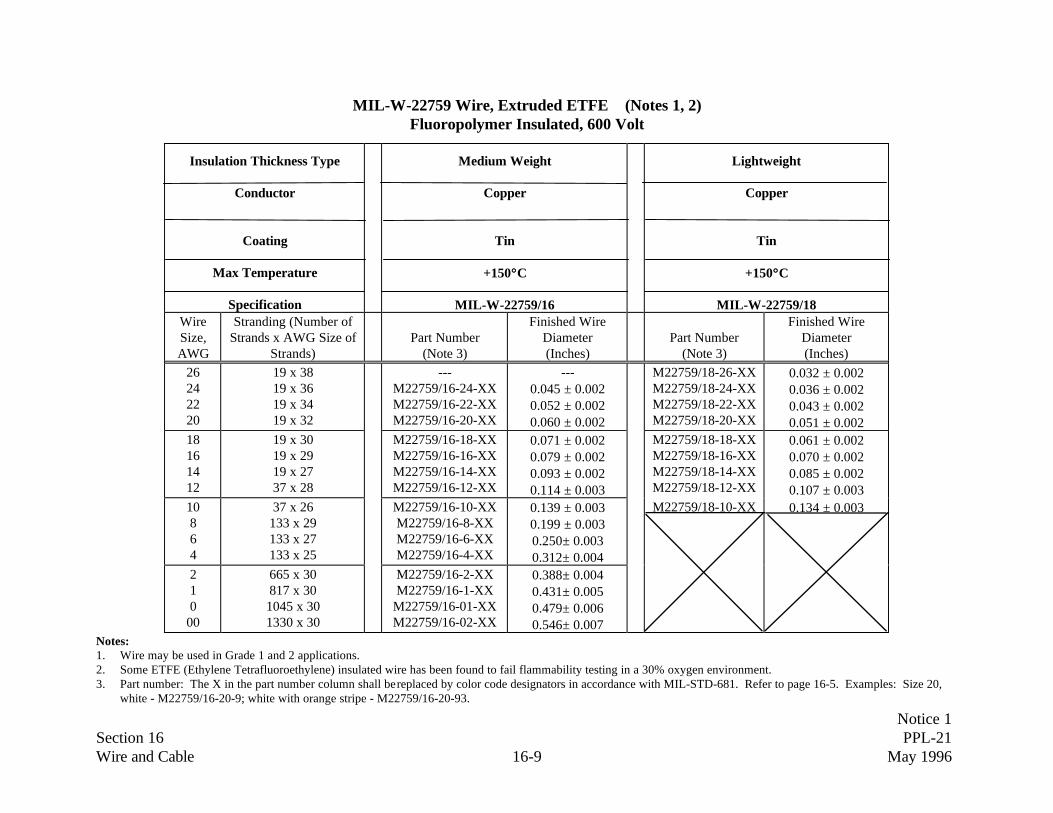
Notice 1Section 16 PPL-21Wire and Cable 16-9 May 1996
MIL-W-22759 Wire, Extruded ETFE (Notes 1, 2)Fluoropolymer Insulated, 600 Volt
Insulation Thickness Type
Conductor
Coating
Max Temperature
Specification
Medium Weight
Copper
Tin
+150°°C
MIL-W-22759/16
Lightweight
Copper
Tin
+150°°C
MIL-W-22759/18WireSize,AWG
Stranding (Number ofStrands x AWG Size of
Strands)Part Number
(Note 3)
Finished WireDiameter(Inches)
Part Number(Note 3)
Finished WireDiameter(Inches)
26242220
19 x 3819 x 3619 x 3419 x 32
---M22759/16-24-XXM22759/16-22-XXM22759/16-20-XX
---0.045 ± 0.0020.052 ± 0.0020.060 ± 0.002
M22759/18-26-XXM22759/18-24-XXM22759/18-22-XXM22759/18-20-XX
0.032 ± 0.0020.036 ± 0.0020.043 ± 0.0020.051 ± 0.002
18161412
19 x 3019 x 2919 x 2737 x 28
M22759/16-18-XXM22759/16-16-XXM22759/16-14-XXM22759/16-12-XX
0.071 ± 0.0020.079 ± 0.0020.093 ± 0.0020.114 ± 0.003
M22759/18-18-XXM22759/18-16-XXM22759/18-14-XXM22759/18-12-XX
0.061 ± 0.0020.070 ± 0.0020.085 ± 0.0020.107 ± 0.003
10864
37 x 26133 x 29133 x 27133 x 25
M22759/16-10-XXM22759/16-8-XXM22759/16-6-XXM22759/16-4-XX
0.139 ± 0.0030.199 ± 0.0030.250± 0.0030.312± 0.004
M22759/18-10-XX 0.134 ± 0.003
210
00
665 x 30817 x 301045 x 301330 x 30
M22759/16-2-XXM22759/16-1-XX
M22759/16-01-XXM22759/16-02-XX
0.388± 0.0040.431± 0.0050.479± 0.0060.546± 0.007
Notes:1. Wire may be used in Grade 1 and 2 applications.2. Some ETFE (Ethylene Tetrafluoroethylene) insulated wire has been found to fail flammability testing in a 30% oxygen environment.3. Part number: The X in the part number column shall be replaced by color code designators in accordance with MIL-STD-681. Refer to page 16-5. Examples: Size 20,
white - M22759/16-20-9; white with orange stripe - M22759/16-20-93.
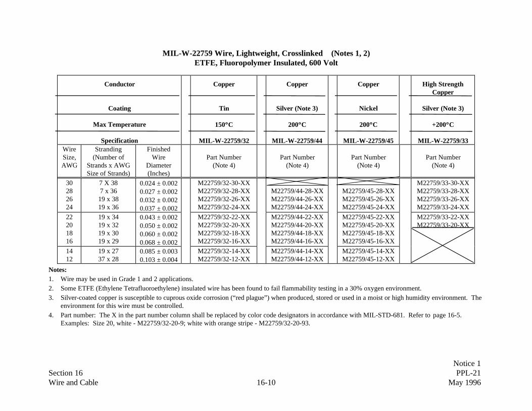
Notice 1Section 16 PPL-21Wire and Cable 16-10 May 1996
MIL-W-22759 Wire, Lightweight, Crosslinked (Notes 1, 2)ETFE, Fluoropolymer Insulated, 600 Volt
Conductor
Coating
Max Temperature
Specification
Copper
Tin
150°°C
MIL-W-22759/32
Copper
Silver (Note 3)
200°°C
MIL-W-22759/44
Copper
Nickel
200°°C
MIL-W-22759/45
High StrengthCopper
Silver (Note 3)
+200°°C
MIL-W-22759/33WireSize,AWG
Stranding(Number of
Strands x AWGSize of Strands)
FinishedWire
Diameter(Inches)
Part Number(Note 4)
Part Number(Note 4)
Part Number(Note 4)
Part Number(Note 4)
30282624
7 X 387 x 36
19 x 3819 x 36
0.024 ± 0.0020.027 ± 0.0020.032 ± 0.0020.037 ± 0.002
M22759/32-30-XXM22759/32-28-XXM22759/32-26-XXM22759/32-24-XX
M22759/44-28-XXM22759/44-26-XXM22759/44-24-XX
M22759/45-28-XXM22759/45-26-XXM22759/45-24-XX
M22759/33-30-XXM22759/33-28-XXM22759/33-26-XXM22759/33-24-XX
22201816
19 x 3419 x 3219 x 3019 x 29
0.043 ± 0.0020.050 ± 0.0020.060 ± 0.0020.068 ± 0.002
M22759/32-22-XXM22759/32-20-XXM22759/32-18-XXM22759/32-16-XX
M22759/44-22-XXM22759/44-20-XXM22759/44-18-XXM22759/44-16-XX
M22759/45-22-XXM22759/45-20-XXM22759/45-18-XXM22759/45-16-XX
M22759/33-22-XXM22759/33-20-XX
1412
19 x 2737 x 28
0.085 ± 0.0030.103 ± 0.004
M22759/32-14-XXM22759/32-12-XX
M22759/44-14-XXM22759/44-12-XX
M22759/45-14-XXM22759/45-12-XX
Notes:1. Wire may be used in Grade 1 and 2 applications.2. Some ETFE (Ethylene Tetrafluoroethylene) insulated wire has been found to fail flammability testing in a 30% oxygen environment.3. Silver-coated copper is susceptible to cuprous oxide corrosion (“red plague”) when produced, stored or used in a moist or high humidity environment. The
environment for this wire must be controlled.4. Part number: The X in the part number column shall be replaced by color code designators in accordance with MIL-STD-681. Refer to page 16-5.
Examples: Size 20, white - M22759/32-20-9; white with orange stripe - M22759/32-20-93.

Notice 1Section 16 PPL-21Wire and Cable 16-11 May 1996
MIL-W-22759 Wire, Normal Weight, Crosslinked (Notes 1, 2)ETFE Fluoropolymer Insulated, 600 Volt
Conductor
Coating
Max Temperature
Specification
Copper
Tin
150°°C
MIL-W-22759/34
Copper
Silver (Note 3)
2000°°C
MIL-W-22759/43
Copper
Nickel
200°°C
MIL-W-22759/41
High StrengthCopper
Silver (Note 3)
200°°C
MIL-W-22759/35WireSize,AWG
Stranding(Number of
Strands x AWGSize of Strands
FinishedWire
Diameter(Inches)
Part Number(Note 4)
Part Number(Note 4)
Part Number(Note 4)
Part Number(Note 4)
26242220
19 x 3819 x 3619 x 3419 x 32
0.040 ± 0.0020.045 ± 0.0020.050 ± 0.0020.058 ± 0.002
M22759/34-24-XXM22759/34-22-XXM22759/34-20-XX
M22759/43-26-XXM22759/43-24-XXM22759/43-22-XXM22759/43-20-XX
M22759/41-26-XXM22759/41-24-XXM22759/41-22-XXM22759/41-20-XX
M22759/35-26-XXM22759/35-24-XXM22759/35-22-XXM22759/35-20-XX
18161412
19 x 3019 x 2919 x 2737 x 28
0.070 ± 0.0030.077 ± 0.0030.094 ± 0.0030.111 ± 0.003
M22759/34-18-XXM22759/34-16-XXM22759/34-14-XXM22759/34-12-XX
M22759/43-18-XXM22759/43-16-XXM22759/43-14-XXM22759/43-12-XX
M22759/41-18-XXM22759/41-16-XXM22759/41-14-XXM22759/41-12-XX
10864
37 x 26133 x29133 x 27133 x 25
0.134 ± 0.0040.195 ± 0.0080.241 ± 0.0100.310 ± 0.010
M22759/34-10-XXM22759/34-8-XXM22759/34-6-XXM22759/34-4-XX
M22759/43-10-XXM22759/43-8-XXM22759/43-6-XXM22759/43-4-XX
M22759/41-10-XXM22759/41-8-XXM22759/41-6-XXM22759/41-4-XX
Notes:1. Wire may be used in Grade 1 and 2 applications.2. Some ETFE (Ethylene Tetrafluoroethylene) insulated wire has been found to fail flammability testing in a 30% oxygen environment.3. Silver-coated copper is susceptible to cuprous oxide corrosion (“red plague”) when produced, stored or used in a moist or high humidity environment. The
environment for this wire must be controlled.4. Part number: The X in the part number column shall be replaced by color code designators in accordance with MIL-STD-681. Refer to page 16-5.
Examples: Size 20, white - M22759/34-20-9; white with orange stripe - M22759/34-20-93.

Notice 1Section 16 PPL-21Wire and Cable 16-12 May 1996
MIL-W-81381 Wire, FEP, Fluorocarbon/Polyimide (Notes 1 through 3) (Page 1 of 2)Insulated, Copper or Copper Alloy
Part Number Explanation:
M81381 /XX -XX -X(X)(X)
Military Specification Detail Specification Wire Size Color CodeNumber (AWG) in accordance
with MIL-STD-681
Notes: (Continued on page 16-13)1. Wire may be used in Grade 1 and 2 applications.2. Tape code: .1/1/.1=0.1 mil Fluorinated Ethylene Propylene (FEP) fluorocarbon resin/1 mil Polyimide film/0.1 mil FEP fluorocarbon. Minimum overlap
50%.3. MIL-W-81381 wire may be preferred for its light weight and excellent mechanical, electrical, and radiation resistance properties. However, the insulation
of this wire has known reliability problems in certain applications. Extended exposure to moisture or alkaline cleaning chemicals has been shown todegrade the insulation’s mechanical strength, resulting in flaking of the outer insulation tape, and cracking from vibration or movement stress wheninstalled around tight radius bends. The resulting degradation may lead to flashover, arc tracking, and shorting, which may ignite the insulation.
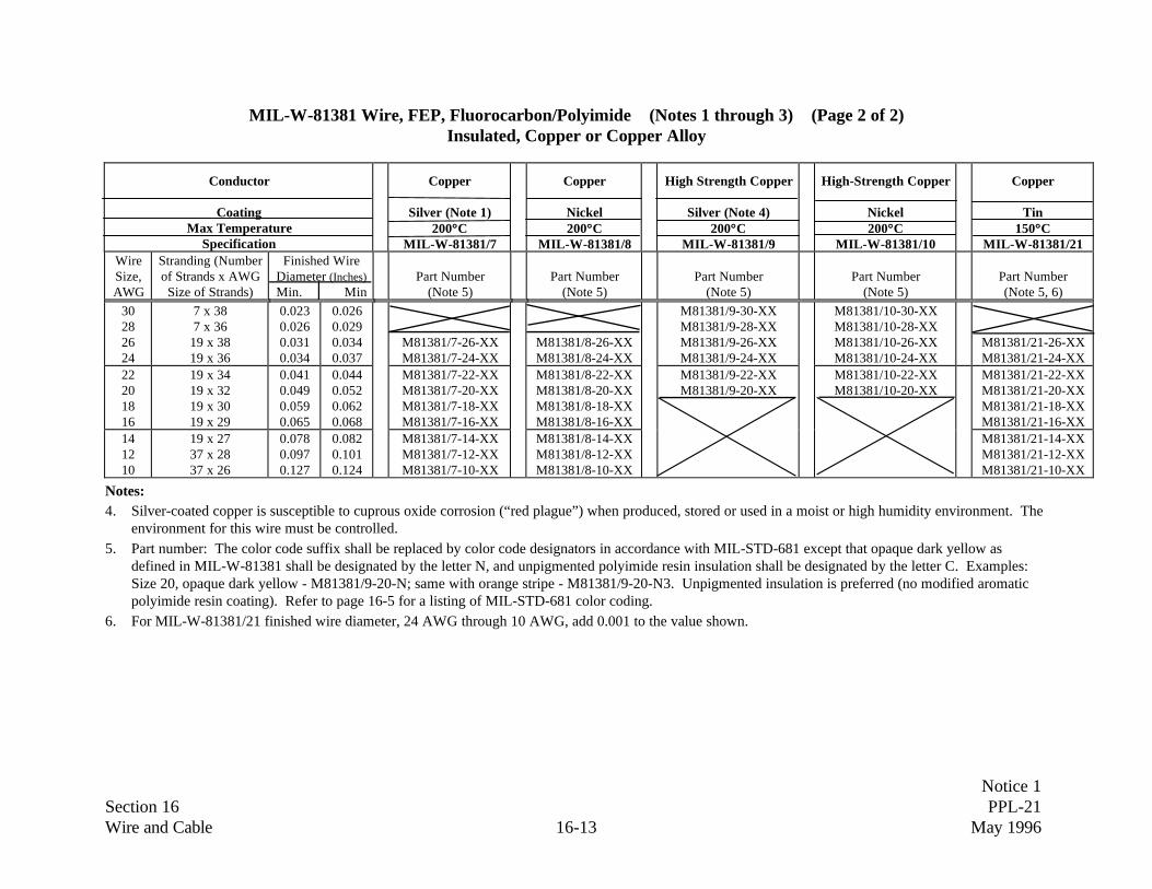
Notice 1Section 16 PPL-21Wire and Cable 16-13 May 1996
MIL-W-81381 Wire, FEP, Fluorocarbon/Polyimide (Notes 1 through 3) (Page 2 of 2)Insulated, Copper or Copper Alloy
Conductor
CoatingMax Temperature
Specification
Copper
Silver (Note 1)200°°C
MIL-W-81381/7
Copper
Nickel200°°C
MIL-W-81381/8
High Strength Copper
Silver (Note 4)200°°C
MIL-W-81381/9
High-Strength Copper
Nickel200°°C
MIL-W-81381/10
Copper
Tin150°°C
MIL-W-81381/21WireSize,AWG
Stranding (Numberof Strands x AWGSize of Strands)
Finished WireDiameter (Inches)Min. Min
Part Number(Note 5)
Part Number(Note 5)
Part Number(Note 5)
Part Number(Note 5)
Part Number(Note 5, 6)
30282624
7 x 387 x 36
19 x 3819 x 36
0.0230.0260.0310.034
0.0260.0290.0340.037
M81381/7-26-XXM81381/7-24-XX
M81381/8-26-XXM81381/8-24-XX
M81381/9-30-XXM81381/9-28-XXM81381/9-26-XXM81381/9-24-XX
M81381/10-30-XXM81381/10-28-XXM81381/10-26-XXM81381/10-24-XX
M81381/21-26-XXM81381/21-24-XX
22201816
19 x 3419 x 3219 x 3019 x 29
0.0410.0490.0590.065
0.0440.0520.0620.068
M81381/7-22-XXM81381/7-20-XXM81381/7-18-XXM81381/7-16-XX
M81381/8-22-XXM81381/8-20-XXM81381/8-18-XXM81381/8-16-XX
M81381/9-22-XXM81381/9-20-XX
M81381/10-22-XXM81381/10-20-XX
M81381/21-22-XXM81381/21-20-XXM81381/21-18-XXM81381/21-16-XX
141210
19 x 2737 x 2837 x 26
0.0780.0970.127
0.0820.1010.124
M81381/7-14-XXM81381/7-12-XXM81381/7-10-XX
M81381/8-14-XXM81381/8-12-XXM81381/8-10-XX
M81381/21-14-XXM81381/21-12-XXM81381/21-10-XX
Notes:4. Silver-coated copper is susceptible to cuprous oxide corrosion (“red plague”) when produced, stored or used in a moist or high humidity environment. The
environment for this wire must be controlled.5. Part number: The color code suffix shall be replaced by color code designators in accordance with MIL-STD-681 except that opaque dark yellow as
defined in MIL-W-81381 shall be designated by the letter N, and unpigmented polyimide resin insulation shall be designated by the letter C. Examples:Size 20, opaque dark yellow - M81381/9-20-N; same with orange stripe - M81381/9-20-N3. Unpigmented insulation is preferred (no modified aromaticpolyimide resin coating). Refer to page 16-5 for a listing of MIL-STD-681 color coding.
6. For MIL-W-81381/21 finished wire diameter, 24 AWG through 10 AWG, add 0.001 to the value shown.

Notice 1Section 16 PPL-21Wire and Cable 16-14 May 1996
GSFC S-311-P-13 Wire, High Voltage, Crosslinked Polyalkene Over Crosslinked PVDF Insulation, (Notes 1, 2)Tin Coated Copper, 135°°C
Part Number Explanation:
311P13 -XX -X(X) -X
GSFC Specification Voltage Rating Wire Size Color CodeNumber 01 = 600 volts (S-311-P-13/1) (AWG) in accordance
02 = 1000 volts (S-311-P-13/2) with MIL-STD-68103 = 2500 volts (S-311-P-13/3)
600 Volt 1000 Volt 2500 Volt
Type DestinationWireSize,
AWG
Stranding(Number of Strands xAWG Size of Strands)
Finished WireDiameter (max)In. (mm)
Stranding(Number of Strands xAWG Size of Strands)
Finished WireDiameter (max)In. (mm)
Stranding(Number of Strands xAWG Size of Strands)
Finished WireDiameter (max)In. (mm)
311P13-XX-30-X311P13-XX-28-X311P13-XX-26-X311P13-XX-24-X
30282624
7 x 387 x 367 x 3419 x 36
0.028 (.71)0.031 (.79)0.035 (.89)0.041 (1.04)
---7 x 367 x 34
19 x 36
--- ---0.034 (.86)0.041 (1.08)0.046 (1.17)
---------
19 x 36
--- ------ ------ ---
0.059 (1.50)311P13-XX-22-X311P13-XX-20-X311P13-XX-18-X311P13-XX-16-X
22201816
19 x 3419 x 3219 x 3019 x 29
0.048 (1.22)0.056 (1.42)0.066 (1.68)0.074 (1.88)
19 x 3419 x 3219 x 3019 x 29
0.053 (1.35)0.061 (1.55)0.074 (1.88)0.082 (2.08)
19 x 3419 x 3219 x 3019 x 29
0.071 (1.80)0.080 (2.03)0.090 (2.29)0.100 (2.54)
311P13-XX-14-X311P13-XX-12-X311P13-XX-10-X311P13-XX-8-X
1412108
19 x 2737 x 28
------
0.090 (2.29)0.122 (2.84)
--- ------ ---
19 x 2719 x 2537 x 26133 x 29
0.098 (2.49)0.127 (3.23)0.142 (3.61)0.208 (5.28)
19 x 2719 x 2537 x 26
133 x 29
0.118 (3.00)0.148 (3.71)0.165 (4.19)0.228 (5.79)
311P13-XX-6-X311P13-XX-4-X311P13-XX-2-X311P13-XX-0-X311P13-XX-00-X
6420
00
---------------
--- ------ ------ ------ ------ ---
---------------
--- ------ ------ ------ ------ ---
133 x 27133 x 25665 x 301045 x 301330 x 30
0.278 (7.06)0.336 (8.53)0.398 (10.1)0.448 (12.4)0.560 (14.2)
Notes:1. For use in Grade 1 and 2 applications.2. Primary insulation is crosslinked extruded Polyalkene. Jacket is crosslinked extruded PVDF.

Notice 1Section 16 PPL-21Wire and Cable 16-15 May 1996
MIL-C-27500 Multiconductor Cable, Shielded and Unshielded, Jacketed and Unjacketed (Note 1)
Part number explanation (Note 2).M27500 X XX XX X(X) X XX
Basic Wire No. Shield Style OuterMilitary Braid Coverage Wire AWG Insulation Type Of Wires and Material Jacket
Specification - = 85% 26 thru 2/0 (Note 4) 1 thru 10 Round Shield with 00=No JacketNumber C = 90% (All conductors PTFE Teflon (Note 5) normal strength copper
(Note 3) are same AWG) LE=Mil-W-22759/9 strands (Note 6) Single JacketRC=Mil-W-22759/11 06=PTFE TeflonRE=Mil-W-22759/12 U = No Shield (White)TK=Mil-W-22759/20 09=FEP TeflonTM=Mil-W-22759/22 Single Shield (White)TN=Mil-W-22759/23 S=Silver 23=Crosslinked
T= Tin ETFE (White)ETFE
TE=Mil-W-22759/16 Double Shield Double Jacket (Note 7)TG=Mil-W-22759/18 W=Silver 59=FEP Teflon
V=Tin (White)Crosslinked ETFE 73=Crosslinked
SB=Mil-W-22759/32 SM=MIL-W-22759/41 ETFE (White)SC=Mil-W-22759/33 SP=MIL-W-22759/43SD=Mil-W-22759/34 SR=MIL-W-22759/44SE=Mil-W-22759/35 SS=MIL-W-22759/45
Notes:1. Cable may be used in Grade 1 or Grade 2 applications.2. Part number explanation is for preferred construction. Use M22759/11 (Symbol RC) or M22759/33 (Symbol SC) for base wire with silver coated copper
single shield (Symbol S) and FEP teflon single jacket (Symbol 09) as first choice. Other options are shown on page 16-3. Example of complete partnumber with above options for three #22 AWG conductors: M27500-22RC3S09 or M27500-22SC3S09. Consult MIL-C-27500 for other options.
3. Designation shown for braid coverage includes preferred conductor identification method (white base color with color spiral stripe.) Optional solididentification color coding is available.
4. Basic wire types are for preferred MIL-W-22759 wire contained in this section.5. Single conductor cable must be shielded and/or jacketed. Otherwise, use one of the basic wire types listed in this section.6. Flat style shield and other shield materials are available. Consult MIL-C-27500.7. The double jacket symbol shall only be used in conjunction with a double shield symbol. The first jacket appears between the two shields and the second
jacket over the outer shield. Both jackets are the same material.
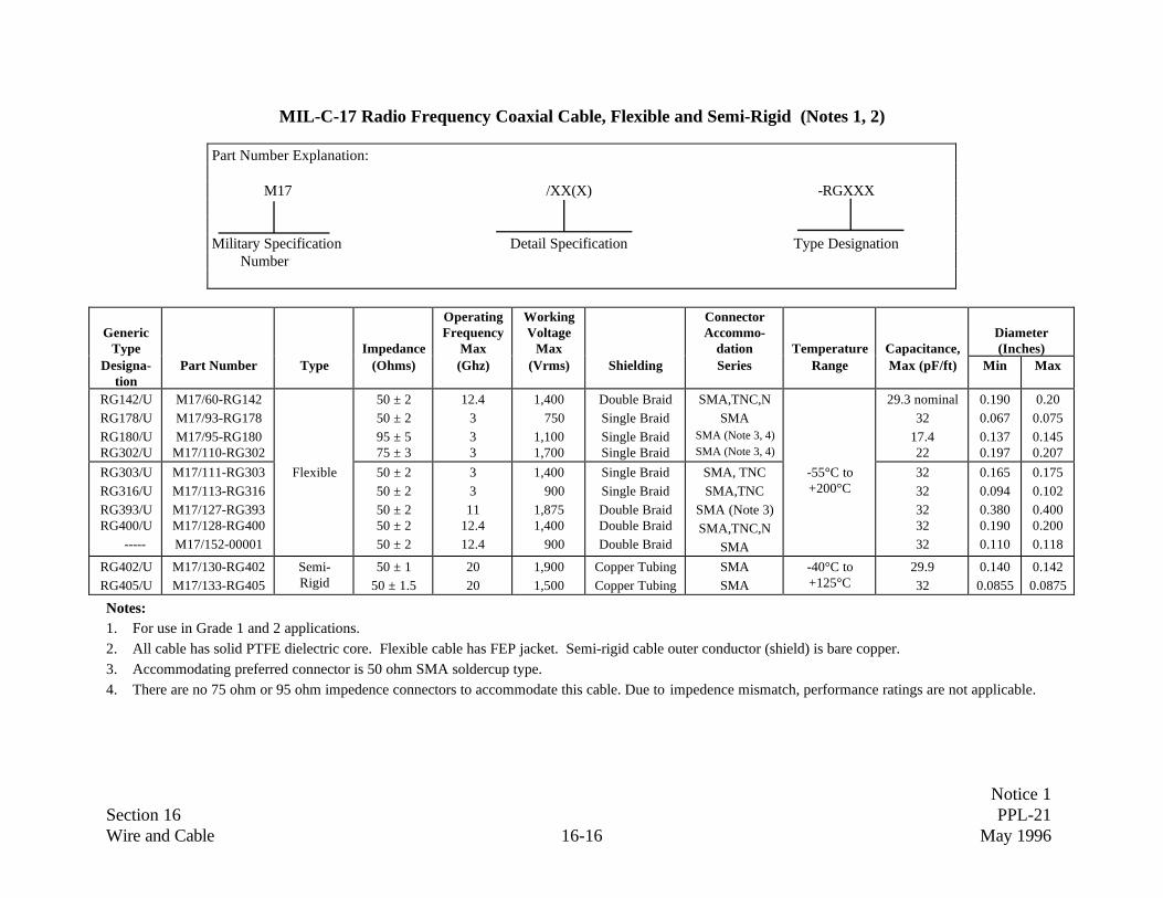
Notice 1Section 16 PPL-21Wire and Cable 16-16 May 1996
MIL-C-17 Radio Frequency Coaxial Cable, Flexible and Semi-Rigid (Notes 1, 2)
Part Number Explanation:
M17 /XX(X) -RGXXX
Military Specification Detail Specification Type DesignationNumber
GenericType Impedance
OperatingFrequency
Max
WorkingVoltage
Max
ConnectorAccommo-
dation Temperature Capacitance,Diameter(Inches)
Designa-tion
Part Number Type (Ohms) (Ghz) (Vrms) Shielding Series Range Max (pF/ft) Min Max
RG142/URG178/URG180/URG302/U
M17/60-RG142M17/93-RG178M17/95-RG180
M17/110-RG302
50 ± 250 ± 295 ± 575 ± 3
12.4333
1,400 7501,1001,700
Double BraidSingle BraidSingle BraidSingle Braid
SMA,TNC,NSMA
SMA (Note 3, 4)SMA (Note 3, 4)
29.3 nominal32
17.422
0.1900.0670.1370.197
0.200.0750.1450.207
RG303/URG316/URG393/URG400/U -----
M17/111-RG303M17/113-RG316M17/127-RG393M17/128-RG400M17/152-00001
Flexible 50 ± 250 ± 250 ± 250 ± 250 ± 2
3311
12.412.4
1,400 9001,8751,400 900
Single BraidSingle BraidDouble BraidDouble BraidDouble Braid
SMA, TNCSMA,TNC
SMA (Note 3)SMA,TNC,N
SMA
-55°C to+200°C
3232323232
0.1650.0940.3800.1900.110
0.1750.1020.4000.2000.118
RG402/URG405/U
M17/130-RG402M17/133-RG405
Semi-Rigid
50 ± 150 ± 1.5
2020
1,9001,500
Copper TubingCopper Tubing
SMASMA
-40°C to+125°C
29.932
0.1400.0855
0.1420.0875
Notes:1. For use in Grade 1 and 2 applications.2. All cable has solid PTFE dielectric core. Flexible cable has FEP jacket. Semi-rigid cable outer conductor (shield) is bare copper.3. Accommodating preferred connector is 50 ohm SMA soldercup type.4. There are no 75 ohm or 95 ohm impedence connectors to accommodate this cable. Due to impedence mismatch, performance ratings are not applicable.

Notice 1Section 16 PPL-21Wire and Cable 16-17 May 1996
J-W-1177 Magnet Wire (Notes 1, 2)
Part Number Explanation:M1177 /X(X) 02 C 0XX
Federal Specification Detail Specification Two Digit Type Code Single Letter Conductor Code Three Digit Size CodeNumber Number 02 - Heavy Insulation C - Copper (Use AWG size of bare wire preceded
by appropriate number of zeros)
SpecificationTemperatureClass (°°C)
J-W-1177/9 (Notes 3, 4)130
J-W-1177/12180
J-W-1177/14200
J-W-1177/15220
InsulationCoating
Solderable PolyurethaneOvercoated with Polyamide,
RoundPolyester-Imide or Polyester-
Amide-Imide, Round
Polyester, Polyester-Imide orPolyester-Amide-Imide, Overcoated
with Polyamide-Imide, RoundPolyimide-Coated, Round
AWG
MaximumOverall
Diameter(inches)
Part Number
MinimumBreakdown
Voltage(volts)
Part Number
MinimumBreakdown
Voltage(volts)
Part Number
MinimumBreakdown
Voltage(volts)
Part Number
MinimumBreakdown
Voltage(volts)
14 0.0682 M1177/9-02C014 5700 M1177/12-02C014 6325 M1177/14-02C014 6325 M1177/15-02C014 632516 0.0545 M1177/9-02C016 5400 M1177/12-02C016 6000 M1177/14-02C016 6000 M1177/15-02C016 600018 0.0437 M1177/9-02C018 5125 M1177/12-02C018 5700 M1177/14-02C018 5700 M1177/15-02C018 570020 0.0351 M1177/9-02C020 4850 M1177/12-02C020 5400 M1177/14-02C020 5400 M1177/15-02C020 540022 0.0281 M1177/9-02C022 4625 M1177/12-02C022 5125 M1177/14-02C022 5125 M1177/15-02C022 512524 0.0227 M1177/9-02C024 4375 M1177/12-02C024 4850 M1177/14-02C024 4850 M1177/15-02C024 485026 0.0182 M1177/9-02C026 4150 M1177/12-02C026 4600 M1177/14-02C026 4600 M1177/15-02C026 460028 0.0147 M1177/9-02C028 3950 M1177/12-02C028 4375 M1177/14-02C028 4375 M1177/15-02C028 437530 0.0119 M1177/9-02C030 3725 M1177/12-02C030 4150 M1177/14-02C030 4150 M1177/15-02C030 415032 0.0098 M1177/9-02C032 3175 M1177/12-02C032 3525 M1177/14-02C032 3525 M1177/15-02C032 352534 0.0078 M1177/9-02C034 2675 M1177/12-02C034 2975 M1177/14-02C034 2975 M1177/15-02C034 297536 0.0063 M1177/9-02C036 2275 M1177/12-02C036 2525 M1177/14-02C036 2525 M1177/15-02C036 252538 0.0051 M1177/9-02C038 1925 M1177/12-02C038 2150 M1177/14-02C038 2150 M1177/15-02C038 2150
40 (Note 2) 0.0040 M1177/9-02C040 1625 M1177/12-02C040 1800 M1177/14-02C040 1800 M1177/15-02C040 180042 (Note 2) 0.0032 M1177/9-02C042 1375 M1177/12-02C042 1525 M1177/14-02C042 1525 M1177/15-02C042 152544 (Note 2) 0.0027 M1177/9-02C044 1175 M1177/12-02C044 1300 M1177/14-02C044 1300 M1177/15-02C044 1300
Notes:1. Magnet wire is intended for use in magnetic devices, rotating equipment and similar applications where a tough film-type insulation providing adequate
mechanical protection is desired.2. For Grade 1 programs, only wire sizes 14 through 38 are acceptable.3. Some QPL suppliers of J-W-1177/9 substitute /42 wire when /9 is ordered. The /42 wire has a temperature rating of 155°C. This substitution is acceptable
to GSFC.4. Due to outgassing concerns of the Nylon coating, M1177/9 wire and M1177/42 wire may not be acceptable for devices with open type construction.

Notice 1Section 16 PPL-21Wire and Cable 16-18 May 1996
THIS PAGE INTENTIONALLY LEFT BLANK

Section 17 PPL-21Crystal Oscillators 17-1 March 1995
Summary of Preferred Crystal Oscillators
ControlSpecification Description
Frequency Range(Hz) Grade 1 Grade 2
Refer toPage No.
MIL-O-55310 Crystal Oscillators, Type 1 0.1 to 60M S B 17-2

Section 17 PPL-21Crystal Oscillators 17-2 March 1995
MIL-O-55310, Crystal Oscillators (Page 1 of 2)
Part Number Explanation
M55310/XX- X XX X XXXXXXXX
Military Specification Product Assurance Level Dash Number Operating Temperature Oscillator Frequencyand Slash Sheet Number S = Class S uniquely identifies Range (Note 1) identified by seven digits
B = Class B performance A = -55°C to +125°C and a letter (H, K, or M)characteristics B = -55°C to + 105°C (Note 2)
Output Frequency
Max. InputCurrentRange Output Voltage
Rise and FallTime Range
Frequency Stability(PPM)
Military PartNumber (Note 3) Classification
Range(Note 4)
@5.25V(ma)
Logic 1(Vdc)
Logic 0(Vdc)
(max)(ns)
-55°C to+125C
-55C to+105°C
Grade1
Grade2
M55310/08-XXXX
M55310/14-XXXX
M55310/16-XXXX
Type 1, HybridConstruction, SquareWave, TTLCompatible, 14 PINDIP
50Hz to 50Mhz
0.1Hz to 25MHz
0.1Hz to 60MHz
25 - 158
20 - 158
30 - 158
2.4 0.5 5 to 15 ± 50 ± 40
S
(Note 5)
S
B
B
B
Notes:1. Temperature range A is available only for Class B oscillators.2. The letters “H”, “K”, “M” represent the decimal point for oscillator frequencies as follows:
H - between 1 and 1000Hz, expressed in Hz.K - between 1KHz and 1MHz, expressed in KHzM - equal to or greater than 1MHz, expressed in MHz.
3. The military part number and the specified nominal frequency (8 characters) define an item of supply.4. The frequency currently available for class S, / 08 oscillator is 512Hz through 1KHz only. The minimum frequency available for Class S, / 16 oscillators is
16khz.5. There are currently no Class S, /14 oscillators available.

Notice 1Section 51 PPL-21Optoelectronics 51-1 May 1996
Optoelectronic Parts
There are no optoelectronic parts that meet the preferred parts criteria specified herein.The listed parts have been evaluated by the GSFC Parts Branch, and/or have been usedsuccessfully in GSFC flight projects, and are provided for information. Lot qualificationand 100% screening tests should be developed and performed on these parts prior toflight usage, and derating criteria should be determined. Recommended screening testsare included in Appendix C. In all cases, a good understanding of photonic partintegration is essential.
Summary of Optoelectronic Parts
SpecificationPart
Number DescriptionRefer toPage No.
S-311-P-339/1 G311P339/1-1 Cable, Fiber Optic, Single Channel, Multimode 51-2MIL-C-83522/2MIL-C-83522/3Commercial
M83522/2-04M83522/3-01501054
SMA ConnectorSMA Coupling BushingSMA Active Device Mount
51-3
MIL-T-29504/4MIL-T-29504/5
M29504/4-4044M29504/5-4050
Termini, Fiber Optic, PinTermini, Fiber Optic, Socket
51-4
S-311-P-762/1S-311-P-763/1
G311P762/1G311P763/1
Transmitter, Digital Integrated, Fiber Optic, TTLReceiver, Digitial Integrated, Fiber Optic, TTLTransceiver, Fiber Optic, MIL-STD-1773 Interface
51-5
S-311-P-614/1 G311P614/1-X Coupler, Fiber Optic, Passive Star 51-6MIL-S-19500/519MIL-S-19500/520MIL-S-19500/521
JANTX1N6609JANTX1N6610JANTX1N6611
LED (Red)LED (Yellow)LED (Green)
51-651-651-6

Notice 1Section 51 PPL-21Optoelectronics 51-2 May 1996
Cable, Fiber Optic, Single Channel, Multimode (Notes 1 through 5)
PartNumber
ManufacturerPart Number
Attenuation(maximum)
Manufacturer
G311P339/1-1 OC-1008 10 dB/km Brand-Rex
Notes:1. G311P339/1-1 cable contains a single 100/140 um size, graded index, optical fiber (Corning SDF) with a double layer acrylate coating. It is a “semi-
loose” tube buffered with a flame retardant polyester elastomer material, contains Teflon TM Impregnated fiberglass strength members, and is jacketed inETFE. The temperature rating is –55°C to 85°C, limited by the acrylate fiber coating.
2. Flammability properties for this cable are controlled by the GSFC specification for ground based levels of oxygen concentrations or lower. Whenapplication conditions expose these parts to pure oxygen levels in excess of 20%, additional flammability hazard analyses should be performed.
3. The manufacturer’s part number listed is for reference only. Part procurement shall be in accordance with GSFC specification S-311-339.4. The ETFE cable jacket has been shown to meet GSFC outgassing requirements.5. Additional radiation tolerant, high temperature cables are being considered for listing in this standard. Contact Code 311 regarding the suitability of cable
types not shown here, or to recommend fiber and cable for evaluation testing.

Notice 1Section 51 PPL-21Optoelectronics 51-3 May 1996
Connector, Fiber Optic, Single Channel (Notes 1 through 5)
PartDescription
Part Number Specification
Manufacturer’sPart Number
Insertion Loss(maximum)
SMA Connector M83522/2-04 MIL-C-83522/2 504019-2 With coupling bushing: 3dB per pairWith device mount: 2 dB
SMA Coupling Bushing M83522/3-01 MIL-C-83522/3 504020-1 See above
SMA Active Device Mount none none 501054 See above
Notes:1. This connector is for use with 100/140 µm size fiber and has use history with the GSFC-S-311-339 cable. Amp Incorporated is the only qualified supplier
for the military part at this time. The device mount, necessary to most optical systems involving SMA connectors, is not shown on the current QPL-83522.The Amp product is recommended here because it will ultimately be the most compatible with the corresponding Amp connector. However, SMA devicemounts are available from a variety of commercial sources.
2. This connector is considered high loss with respect to available commercial designs for single fiber connectors. It is a non-keyed, non-contact connectorand can show insertion loss variability (up to 1.5 dB) with every break-and-mate action. Use of a 4 in-lb torque wrench during mating may reduce some ofthis variability.
3. Flight connector coupling rings should be staked in place to reduce any backing off of the connector with excessive exposure to vibration and elliminateunessessary breaking of the connection.
4. The preferred epoxy for use with this connector is Trabond BA-F253 (as opposed to the types listed in the military specification). Use of TRMM-733-192,Optical Fiber Cable Termination Procedure for MIL-C-83522/2 Optical Fiber Connectors is recommended when using these connectors.
5. The Parts Branch is investigating qualification of less lossy single fiber connectors for future use by GSFC projects. Please contact the Parts Branch forinformation regarding other single fiber connectors or to make suggestions in this regard.
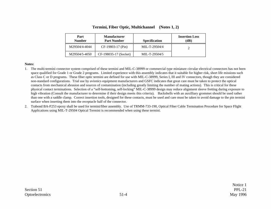
Notice 1Section 51 PPL-21Optoelectronics 51-4 May 1996
Termini, Fiber Optic, Multichannel (Notes 1, 2)
PartNumber
ManufacturerPart Number Specification
Insertion Loss(dB)
M29504/4-4044 CF-19803-17 (Pin) MIL-T-29504/4 2
M29504/5-4050 CF-198035-17 (Socket) MIL-T-29504/5
Notes:1. The multi-termini connector system comprised of these termini and MIL-C-38999 or commercial type miniature circular electrical connectors has not been
space qualified for Grade 1 or Grade 2 programs. Limited experience with this assembly indicates that it suitable for higher risk, short life missions suchas Class C or D programs. These fiber optic termini are defined for use with MIL-C-38999, Series I, III and IV connectors, though they are considerednon-standard configurations. Trial use by avionics equipment manufacturers and GSFC indicates that great care must be taken to protect the opticalcontacts from mechanical abrasion and sources of contamination (including greatly limiting the number of mating actions). This is critical for thesephysical contact terminations. Selection of a “self-bottoming, self-locking” MIL-C-38999 design may reduce alignment sleeve fretting during exposure tohigh vibration (Consult the manufacturer to determine if their design meets this criteria). Backshells with an auxilliary grommet should be used ratherthan one with a saddle clamp. Correct insertion tools, designed for these contacts, must be used and care must be taken to avoid damage to the pin terminisurface when inserting them into the receptacle half of the connector.
2. Trabond BA-F253 epoxy shall be used for termini/fiber assembly. Use of TRMM-733-190, Optical Fiber Cable Termination Procedure for Space FlightApplications using MIL-T-29504 Optical Termini is recommended when using these termini.

Notice 1Section 51 PPL-21Optoelectronics 51-5 May 1996
Transmitter, Digital Integrated, Fiber Optic, TTL (Notes 1 through 3)
PartNumber
Manufacturer Part Number(Notes 1, 2) Manufacturer
Light Power Coupled toFiber (Note 3)
OutputWavelength Vcc Icc
G311P762/1 HFE4811-014 Honeywell 100 µW 850 nm 5.0 V 65 mA
Notes:1. This part has been used in flight hardware by several GSFC projects and may be suitable for future applications. Its usage history indicates that each flight
lot should be qualified separately, and all parts shall be 100% screened in accordance with the requirements of S-311-P-762/1.2. The emitter used in this transmitter is the HFE4010-014 and may be bought as an individually packaged device.3. 100/140 µm size fiber with NA=0.29 (see S-311-339/1-1).
Receiver, Digital Integrated, Fiber Optic, TTL (Notes 1, 2)
PartNumber
Manufacturer Part Number(Note 1) Manufacturer Sensitivity Vcc Icc
G311P763/1 HFE3801-002 Honeywell 1 µW 5.0 V 20 mA
Notes:1. This part has been used in flight hardware by several GSFC projects and may be suitable for future applications. Its usage history indicates that each flight
lot should be qualified separately, and all parts shall be 100% screened in accordance with the requirements of S-311-P-763. The requirements of S-311-200, General Requirements for Hybrid Microcircuits, shall apply.
2. The detector used in this transmitter is the HFD3000-002 and may be bought as an individually packaged device.
Transceiver, Fiber Optic, MIL-STD-1773 Interface
Fiber optic transceivers for use with MIL-STD-1773 databus applications have beenused by several GSFC projects in the past. This part is currently being redesigned bythe manufacturer, SCI Systems Inc. Please contact the Parts Branch for informationabout the availability of this part or replacement options.

Notice 1Section 51 PPL-21Optoelectronics 51-6 May 1996
Coupler, Fiber Optic
PartNumber
Attenuation(Max) Manufacturer
Manufacturer PartNumber
G311P614/1-X (Note 1) 16 dB Canstar SFC-C-20X20-S20
Notes:1. Based on the GSFC evaluation, couplers with two to 10 fused fibers (four to 20 ports) may be specified.
Diodes, Light Emitting (LEDs)
MIL-S-19500Part Number
MIL-S-19500Slash Sheet
Relative Light Power Output(Minimum)
Wavelength(Color)
JANTX1N6609
JANTX1N6610
JANTX1N6611
/519
/520
/521
120 mW (IFMAX = 35mA)
120 mW (IFMAX = 35mA)
120 mW (IFMAX = 35mA)
Red
Yellow
Green

Notice 1PPL-21
Appendix A A-1 May 1996
Table 01 Additional Testing Requirements for Preferred Capacitors
Test Methods, MIL-C-20 MIL-C-39003 MIL-C-55681
Inspection/Test Conditions and Requirements Grade 1 Grade 2 Grade 1 Grade 2 Grade 1 Grade 2
Humidity, Steady State,Low Voltage
MIL-C-123, Table XI, GroupB, Subgroup 2.
12 (0) 12 (0)
Surge Current MIL-C-39003/10 100%(Note 1)
Destructive PhysicalAnalysis
MIL-C-123, Table X, Group A,Subgroup 3
5 (0) 5 (0)
Notes:1. Required for styles CSR09, CSR13, CSR21 and all CWR styles.

Notice 1PPL-21
Appendix A A-2 May 1996
Table 02 Additional Testing Requirements for Preferred Connectors (Note 1) (Page 1 of 3)
Test Methods, Connector Type/Grade LevelInspection/ Conditions and Circular D-Subminiature Microminiature Printed Circuit
Test Requirements 1 2 1 2 1 2 1 2Visual Inspection Verify proper marking, free of
workmanship defects in accordance withTable 02A. 3X magnification (min.) andhigh intensity lighting.
X X X X X X X X
Mechanical Inspection Verify design, construction, dimensions,materials and finish.
X 2 (0) X 2 (0) X 2 (0) X 2 (0)
Dielectric Withstanding Voltage(Sea Level)
MIL-STD-1344, Method 3001. Refer toreference specifications for voltages,mating requirements.
X X X X
Insulation Resistance MIL-STD-1344, Method 3003, ConditionB. 5000 megohms min. in accordancewith reference specifications.
X X X X
Outgassing Control(As required)
(Note 4) X X X X
Hermeticity(Sealed Receptacles Only)
MIL-STD-1344, Method 1008, Pressureas specified.
X 2 (0)
See notes on page A-4.
(Note 3)

Notice 1PPL-21
Appendix A A-3 May 1996
Table 02 Additional Testing Requirements for Preferred Connectors (Note 1) (Page 2 of 3)
Test Methods, Connector Type/Grade LevelInspection/ Conditions and Radio
FrequencyContacts EMI
Filter PinHigh
VoltageTest Requirements 1 2 1 2 1 2 1 2
Visual Inspection Verify proper marking, free ofworkmanship defects in accordance withTable 02A. 3X magnification (min.) andhigh intensity lighting.
X X X X X X X X
Mechanical Inspection Verify design, construction, dimensions,materials and finish.
X 2 (0) X 2 (0) X 1(0) X 2 (0)
Dielectric Withstanding Voltage(Sea Level)
MIL-STD-1344, Method 3001.MIL-STD-202, Method 301 for RFconnectors. Refer to referencespecifications for voltages, matingrequirements.
2 (0)2 (0) X X
Insulation Resistance MIL-STD-202, Method 302 for RFconnectors and filter pins. 5000megohms min. in accordance withreference specifications.
2 (0) X
Outgassing Control(As required)
(Note 4) X X X X X X X X
Hermeticity(Sealed Receptacles Only)
MIL-STD-202, Method 112, ConditionC, Procedure III. Pressure as specified.
X
See notes on page A-4.
(Note 8)(Note 7)(Note 6)(Note 5)

Notice 1PPL-21
Appendix A A-4 May 1996
Table 02 Additional Testing Requirements for Preferred Connectors (Page 3 of 3)
Notes:1. An “X” in the table indicates that the inspection/test is to be performed on a 100% basis. Y (0) indicates the quantity (accept number) for sample testing.
If a failure occurs during sample testing, the tests shall either be performed on a 100% basis or the sample size shall be tripled and the tests repeated. If afailure occurs during the second sample test, the lot shall be rejected. 100% examination may be performed at the user’s receiving and inspectionfacilities in lieu of performance by the manufacturer.
2. Required only for MIL-C-26482 and MIL-C-5015 connectors.
3. For MIL-C-83513 microminiature connectors with crimp type pig tail leads, adjacent leads shall be tested for shorting prior to DWV. Each lead shall betested. A test potential of 600 VRMS (Sea Level) shall be used. If manufacturer can certify that this test is normally performed on each connector,additional testing is not required.
4. a. The user may process connectors for outgassing control by removing and replacing lubricant with a low outgassing lubricant followed by a bakeout of24 hours at 125°C. Low outgassing lubricants as well as other acceptable variations of bakeout time, temperature, and vacuum for outgassing controlare contained in NASA Reference publication 1124. Since removal and replacement of lubricant requires disassembly and is labor intensive, it isrecommended that this processing be performed by the manufacturer on connectors procured to a controlled specification.
b. Microminiature receptacles contain a fluorosilicone or silicone rubber interface seal. Silicone rubber seals may be an outgassing concern. Theinterface seal can be carefully removed with small tweezers and discarded. Otherwise, a bakeout of 24 hours at 125°C is recommended to controloutgassing.
c. Type SMA RF connector plugs may contain a silicone rubber O-Ring interface seal inside the coupling nut, on the mounting flange or inside the cablenut, and require either replacement with flurosilicone O-Rings or a 125°C bakeout for 24 hours to prevent outgassing.
d. High voltage panel mount receptacle connectors contain a small silicone rubber grommet which surrounds the center pin contact. This grommet is anoutgassing concern, and a bakeout of 125°C is recommended for outgassing control.
5. For coaxial connectors, the connector shall be terminated to the appropriate coaxial cable, and the applied voltage shall be as specified in the detailspecification.
6. For coaxial contacts, the dielectric withstanding voltage test shall be performed in accordance with MIL-STD-1344, Method 3001. A voltage of 1000VRMS (Sea Level) shall be applied between inner contact and shell.
7. For filter pin connectors, dielectric withstanding voltage of twice the rated dc voltage shall be applied for five to ten seconds between each contact and theshell. Current shall be limited to 20 milliamps.
8. High voltage connectors have voltage ratings in excess of 5KV and are similar to Reynolds part numbers 167-3770 and 167-3771. For high voltageconnectors rated at 10KVDC, a potential of 15KVDC shall be applied to each connector for 10 seconds, minimum.

Notice 1PPL-21
Appendix A A-5 May 1996
Table 02A Inspection Criteria for Connectors and Contacts (Note 1)
DEFECT Circulars DSUBSMicro-
miniature PC RF ContactsRF
ContactsFilterPin
HighVoltage
INSERTInsert to Shell Positioning andOrientationCracks, ChipsMarkingNegative Meniscus of Glass
(Hermetics only-glass to contact andglass to shell)
GROMMETNicks, Gougles, Tears, FoldsMarking
SHELLSCracks, Dents, ScratchesFinish (Peeled or blistered plating, discoloration, exposed base metal)Marking Completeness, LegibilitySleeves (Fixed - Not free to move)
THREADS (As Applicable)Nicks, Dents, Voids
ADHESIVESExcess Bonding Material (Overflow)Voids
XXXX
X
XXX
XXX
X
XX
XXX
XXX
X
XXX
X
XXX
XXX
X
XXX
X
XXX
X
XX
XXX
XXX
X
XXX
X
XX
XXX
XXX
XX
XXX
XXX
XX
XXXX
XXX
X
XXX
XXX
XX
XXX
XX
XXX
See notes on page A-4.

Notice 1PPL-21
Appendix A A-6 May 1996
Table 04 Additional Testing Requirements for Preferred FM08/FM04 Fuses
Inspection/Test Test Methods, Conditions, and Requirements Notes
Visual Inspections Materials, design, construction, marking, andworkmanship
Resistance (Cold) MIL-STD-202, Method 303Resistance to specification 1
Voltage Drop (Hot-1) 100% rated current for 5 minutes (minimum)Voltage drop to specification (when specified) 2
Thermal Shock MIL-STD-202, Method 107Condition B 3, 4
Voltage Drop (Hot-2) 100% rated current for 5 minutes (minimum)Ratio voltage drop:
(Hot-1/Hot-2) = 0.97 to 1.03Resistance (Cold) MIL-STD-202, Method 303
Resistance to specification 1
Seal MIL-STD-202, Method 112Test Condition A
Notes:1. The source current for the resistance measurement shall not exceed 10% of the nominal current rating at room temperature.2. The voltage drop (hot ) measurement must be recorded to calculate the voltage drop ratio regardless of whether or not it is a specification requirement.3. Fuses rated at < +125°C shall be tested to Condition A.4. External visual examination is required after testing to verify no evidence of mechanical damage.

Notice 1PPL-21
Appendix A A-7 May 1996
Table 07 Additional Testing Requirements for Preferred M83401 Resistor Networks
Inspection Method Requirement
Thermal Shock MIL-R-83401Para. 4.6.3
MIL-R-83401Para. 3.7
Power ConditioningMIL-R-83401
Para. 4.6.4The following exception shall apply:burn-in time = 150 hours minimum
MIL-R-83401Para. 3.8
DC Resistance ∆R and final resistance to specificationper paras. 3.8 and 3.9 of MIL-R-83401
Table 08 Additional Testing Requirements for Preferred Diodes (Note 1)
Test Methods, Sample Size
Inspection/Test Conditions, and Requirements Grade 1 Grade 2
PIND(Note 2)
MIL-STD-750, Method 2052, Condition A Not Required for JAN S 100%
Notes:1. Not required for non-cavity parts2. When procured directly from the manufacturer with PIND testing in accordance with Paragraph 4.6.3.4 of MIL-S-19500, additional testing is not required.
Table 09 Additional Testing Requirements for Preferred Transistors
Test Methods, Sample Size
Inspection/Test Conditions, and Requirements Grade 1 Grade 2
PIND(Note 1)
MIL-STD-750, Method 2052, Condition A Not Required for JAN S 100%
Notes:1. When procured directly from the manufacturer with PIND testing in accordance with Paragraph 4.6.3.4 of MIL-S-19500, additional testing is not required.

Notice 1PPL-21
Appendix A A-8 May 1996
Table 10 Additional Testing Requirements for Preferred Microcircuits
Test Methods, Sample Size
Inspection/Test Conditions, and Requirements Grade 1 Grade 2
PIND MIL-STD-883, Method 2020, Condition A Not Required for ClassS, V, K
100%
Table 17 Additional Testing Requirements for Preferred Crystal Oscillators
Sample Size
Inspection/Test Test Methods, Conditions, and Requirements Grade 1 Grade 2
PIND MIL-STD-883, Method 2020, Condition B Note 1 100%
Radiographic Inspection MIL-STD-202, Method 209, 1 view in Y Direction,2nd view 90° relative to first view
Note 1 100%Note 2
Internal Water Vapor Content MIL-STD-883, Method 1018 3 (0) or 5 (1) 3 (0) or 5 (1)
Notes:1. Not required for MIL-O-55310 Class S Oscillators. Tests are performed in screening.2. Not required for devices of discrete component construction.

Notice 1PPL-21
Appendix B B-1 May 1996
Table 01 Capacitor Derating Criteria
Voltage derating is accomplished by multiplying the maximum operating voltage by the appropriate deratingfactor appearing in the chart below.
Type MilitaryStyle
VoltageDerating Factor
MaximumAmbient
Temperature
Ceramic CCR, CKS, CKR, CDR (Note 1) 0.60 110°C
Glass CYR 0.50 110°C
Plastic Film CRH, CHS 0.60 85°C
Tantalum, Foil CLR25, CLR27, CLR35, CLR3 0.5 70°C
Tantalum, Wet Slug CLR79, CLR81 0.600.40 (Note 2)
70°C110°C
Tantalum, Solid (Note 3) CSR, CSS, CWR 0.500.30 (Note 2)
70°C110°C
Notes:1. For low-voltage applications (<10 Vdc), rated voltage shall be at least 100 Vdc for Styles CCR, CKR, CDR.2. Derate voltage linearly from 70°C to 110°C.3. The effective series resistance shall be at least 0.1 ohms per volt or 1 ohm, whichever is greater, for Grade 2
applications, and at least 0.3 ohms per volt for Grade 1 applications.
Table 02 Connector Derating Criteria
Type/StyleVoltage DeratingFactor (Note 1)
Maximum AmbientTemperature
All 0.25 Rated temperature minus 25°C
Notes:1. Voltage derating factor is given as a percentage of the sea level Dielectric Withstanding Voltage.
Table 03 Filter Derating Criteria
ClassStress Parameter
(Note 1)DeratingFactor
Rated current 0.50
All Rated voltage 0.50
Maximum AmbientTemperature
85°C or 30°C less thanmaximum rated temperature,
whichever is less
Notes:1. Applies to rated operating current or voltage, not the absolute maximum.

Notice 1PPL-21
Appendix B B-2 May 1996
Table 04 Fuse Derating Criteria (Notes 1-4)
Fuse Current Rating(Amperes)
Derate to the Following (%) ofRated Current Remarks
15, 10, 7, 5, 4, 3, 2, 2-1/2, 2 50%1-1/2, 1 45%
3/4 40%1/23/81/41/8
40%35%30%25%
The flight use of fuses rated 1/2ampere or less requiresapplication approval by thecognizant GSFC project office.
Notes:1. Fuses are specified to interrupt within a maximum of five seconds when driven at 200% of their rated current
for nominal ratings up to and including 10 amperes. A fuse with a nominal rating of 15 amperes is specifiedto interrupt within a maximum of ten seconds when driven at 200% of its rated current.
2. Derating of fuses allows for possible loss of internal gases in a space environment which reduces heat transferby conduction. This lowers the blow current rating and decreases current capability with time.
3. Additional derating of the lower current rated fuses allows for the smaller geometries which reduce heattransfer by conduction.
4. Derating factors are based on data from fuses mounted on printed circuit boards and conformally coated.Other type mountings require GSFC project office approval.
Table 05 Coil/Inductor Derating Criteria (Note 1)
Type ClassInsulation Stress Parameter
MinimumDerating
MIL-C-39010/15305OABF
Rated operating temperature85°C105°C125°C150°C
65°C85°C
105°C130°C
All Rated operating voltage 50% of rated dielectricwithstanding voltage
Notes:1. a. Maximum operating temperature equals ambient temperature plus temperature rise plus 10°C allowance
for hot spots. The temperature rise may be calculated in accordance with MIL-T-27, paragraph 4.8.12.b. The insulation classes of MIL- style inductive parts generally have operating temperature ratings based on
a life expectancy of 10,000 hours. The derated operating temperatures are selected to extend the lifeexpectancy to 50,000 hours at rated voltage.
c. Custom made inductive devices shall be evaluated on a materials basis to determine the maximumoperating temperature. Devices with temperature ratings different from the military insulation classesshall be derated to 0.75 times maximum operating temperature.

Notice 1PPL-21
Appendix B B-3 May 1996
Table 06 Relay Derating Criteria (Note 1)
Style Make, Break, and/or Carry Load Currents Transient Current Surges (Note 3)
AllSelect the appropriate factors for T, R, and Lfrom the subtables:
Iderated = Irated x T x R x L (Note 2)
For t ≤ 10µs,Imax ≤ 4 x Irated
For t > 10 µs,(Imax)2 x t ≤ 16 x (Irated)2 x 10⁻⁵ (A2s)
Notes:1. WARNING: Do not derate coil voltage or current. Operating a relay at less than nominal coil rating can
result in either switching failures or increased switching times. The latter condition induces contact damagebecause of the longer arcing time, thus reducing relay reliability.
2. Iderated = derated contact current carrying capacityIrated = rated contact current
3. If during switching, transient current surges exceed the derated contact current, the following applies, where:t = period of time that transient current exceeds rated contact current (Irated)Imax = maximum permitted surge currentIrated = rated contact current
Subtable T
TemperatureRange Factor
+85°C to+125°C
0.7
+40°C to+84°C
0.85
-20°C to +39°C 0.9-65°C to -21°C 0.85
Subtable R
Cycle Rateper Hour Factor
>10 0.851 to 10 0.90
<1 0.85
Subtable L
LoadApplication Factor
Make, break and/or carry loadswith an on-time duration of 0to 500 ms. Off-time is equal toor greater than on-time.
1
Carry-only loads. Relay doesnot make or break the load.Maximum on-time is 5minutes. Off-time is equal toor greater than on-time.
1.5
All other load conditions. 0.8

Notice 1PPL-21
Appendix B B-4 May 1996
Table 07 Resistor Derating Criteria
Style DescriptionDeratingFactors
(Note 1) (Note 2)
DeratingTemperatures
(°C)
ZeroPowerTemp.(°C)
Power Voltage T1 T2 T3
G311P672 Fixed, High Voltage 0.6 0.8 70 94 110G311P683 Fixed, Precision, High Voltage 0.6 0.8 125 185 225G311P742 Fixed, Low TC, Precision 0.6 0.8 125 155 175RBR
1%0.5%0.1%
Fixed, Wirewound (Accurate), ER0.60.350.25
0.80.80.8
125125125
137132130
145145145
RWR Fixed, Wirewound (Power Type), ER 0.6 0.8 25 160 250RCR Fixed, Composition (Insulated), ER 0.6 0.8 70 (Note 3) (Note 3)RER Fixed, Wirewound (Power Type),
Chassis Mounted, ER0.6 0.8 25 160 250
RTR Variable, Wirewound (Lead ScrewActuated), ER
0.6 0.8 85 124 150
RLR100ppm350ppm
Fixed, Film (Insulated), ER0.60.6
0.80.8
7070
118103
150125
RNX Fixed, Film, ER 0.6 0.8 125 155 175RM Fixed, Film, Chip, ER 0.6 0.8 70 118 150RZ Fixed, Film, Networks 0.6 0.8 70 103 125Others Various 0.5 0.8 (Note 4) (Note 4) (Note 4)
Notes:1. Compute the resistor’s derated power level by multiplying its nominal power rating by the appropriate derating
factor for ambient temperatures ≤ T1. If the resistor is operated above T1, derate linearly from the T1 powerlevel to the zero power level at T2. Exposing the resistor to temperatures exceeding T3, even under no loadconditions, may result in permanent degradation.
2. The maximum applied voltage shall not exceed the lesser of the following: (1) 80% of the specified maximumvoltage rating, or (2) √PR
whereP = Derated power (Watts)R = Resistance of that portion of the element actually active in the circuit.
This voltage derating applies to dc and regular ac waveform applications. For pulse and other irregularwaveform applications, consult MIL-HDBK-978 or the manufacturer.
3. Determine the zero power temperature (T3) from the applicable detail specification. Compute the derated zeropower temperature (T2) from the following formula:
T2 = DF(T3-T1) + T1where:
T2 = Derated zero power temperatureDF = Derating factorT3 = Zero power temperatureT1 = Rated power temperature
4. Determine the rated power, the rated power temperature (T1), and the zero power temperature (T3) from themanufacturer’s specification. Calculate the derated zero power temperature (T2) as per the previous note.

Notice 1PPL-21
Appendix B B-5 May 1996
Table 08 Diode Derating Criteria
Diode Type Stress ParameterDeratingFactor
General purpose, PIV 0.70Rectifier, Switching, Surge current 0.50Pin/Schottky, and Forward current 0.50Thyristors Maximum Junction Temperature 0.80
Power 0.50Varactor Reverse voltage 0.75
Forward current 0.75Maximum Junction Temperature 0.80
Voltage Power 0.50Regulator Zener current 0.5(Izmax + Iznom)
Maximum Junction Temperature 0.80Voltage Zener current N/Areference Maximum Junction Temperature 0.80Zener Voltage Power dissipation 0.50Suppressor Maximum Junction Temperature 0.80Bidirectional Voltage Power dissipation 0.50Suppressor Maximum Junction Temperature 0.80FET Current Regulator Peak operating voltage 0.80
Maximum Junction Temperature 0.80
Table 09 Transistor Derating Criteria
TypeStress
ParameterDeratingFactor
Power 0.60
All Current 0.75
(Note 2) Voltage (Note 1) 0.75
Junction Temperature 0.80
Notes:1. Worst-case combination of DC, AC, and transient voltage should be no greater than the derated limit.2. For power MOSFET devices, also derate the gate to source voltage (VGS) to 60% of the maximum rated value.

Notice 1PPL-21
Appendix B B-6 May 1996
Table 10 Microcircuit Derating Criteria (Note 1)
Derating FactorStress Parameter Digital Linear
Maximum SupplyVoltage/Input Voltage (Note 1)
0.9 0.9
Power Dissipation 0.8 0.75
Maximum Specified OperatingJunction Temperature (Note 2)
0.8 0.75
Maximum Output Current 0.8 0.8
Notes:1. Use manufacturer’s recommended operating conditions but do not exceed 90% of maximum supply voltage.
For voltage regulators, derate VIN - VOUT to 0.9.2. Do not exceed Tj = 100°C for silicon digital microcircuits or Tj = 93.5°C for silicon linear microcircuits.
Table 14 Thermistor Derating Criteria (Note 1)
Type Derating
Positive Temperature Coefficient Derate to 50% of rated power.
Negative Temperature Coefficient Derate to a power level causing a maximum increaseof 50 times the dissipation constant, or a maximumcase temperature of 100°C, whichever is less.
Notes:1. Derating is applicable to thermistors operating in the self-heating mode.
Table 15 Transformer Derating Criteria (Note 1)
Type ClassInsulation Stress Parameter
MinimumDerating
MIL-T-27
Q
R
S
Rated operating temperature
85°C
105°C
130°C
65°C
85°C
110°C
All Rated operating voltage 50% of rated dielectricwithstanding voltage
Notes:1. a. Maximum operating temperature equals ambient temperature plus temperature rise plus 10°C allowance
for hot spots. The temperature rise may be calculated in accordance with MIL-T-27, paragraph 4.8.12.b. The insulation classes of MIL- style inductive parts generally have operating temperature ratings based on
a life expectancy of 10,000 hours. The derated operating temperatures are selected to extend the lifeexpectancy to 50,000 hours at rated voltage.
c. Custom made inductive devices shall be evaluated on a materials basis to determine the maximumoperating temperature. Devices with temperature ratings different from the military insulation classesshall be derated to 0.75 times maximum operating temperature.

Notice 1PPL-21
Appendix B B-7 May 1996
Table 16 Wire and Cable Derating Criteria (Note 1, 2, 3)
Derated Current (Amperes)
Wire Size (AWG) Single Wire Bundled Wire or Cable
30 1.3 0.728 1.8 1.026 2.5 1.424 3.3 2.022 4.5 2.520 6.5 3.718 9.2 5.016 13.0 6.514 19.0 8.512 25.0 11.510 33.0 16.58 44.0 23.06 60.0 30.04 81.0 40.02 108.0 50.00 147.0 75.0
00 169.0 87.5Notes:1. Derated current ratings are based on an ambient temperature of 70°C or less in a hard vacuum of 10 -6 torr.2. The derated current ratings are for 200°C rated wire, such as Teflon insulated (Type PTFE) wire, in a hard
vacuum of 10-6 torr.a. For 150°C wire, use 80% of value shown in Table 16.b. For 135°C wire, use 70% of value shown in Table 16.c. For 105°C wire, use 50% of value shown in Table 16.
3. The current rating for bundles or cables are based on bundles of 15 or more wires. For smaller bundles, theallowable current shall be determined by IBW = ISW x (29-N)/28 where N = number of wires, IBW = current,bundled wire and ISW = current, single wire.

Notice 1PPL-21
Appendix B B-8 May 1996
THIS PAGE INTENTIONALLY LEFT BLANK

PPL-21Appendix C C-1 March 1995
Table 01 Capacitor Screening Requirements (Page 1 of 3)
Part Type/Grade Level
Inspection/Test
Test Methods,Conditions andRequirement
(Note 1)Ceramic Plastic Tantalum Glass Mica Variable
RFIFeed-Thru
SwitchModePowerSupply
1 2 1 2 1 2 1 2 1 2 1 2 1 2 1 21. a. Visual and
mechanicalExamination.
b. ElectricalMeasurements
Optional for all grades.Same as step 10 and step5.
2. Thermal Shock MIL-STD-202, Method107, Condition B, -55°Cto +125°C
X X X X X X X X X X X X X X X X
3. Voltage Conditioning(Burn-In)
2 x Rated Voltage,125°C, 160 hours
140% rated voltage,125°C, 48 hours
1.2 x rated AC voltage atmaximum ratedfrequency, 160 hours
Rated voltage 85°C, 48hours
3 x rated voltage roomtemp., 48 hours
X X
X X
X X
X X
X X
X
X
X
X X
4. Surge Current MIL-C-39003/10 X5. High Impedance
temp. and voltageramp (Note 2)
5 cycles, -55°C to 100°Cin accordance withMIL-C-872147 4.7.4
X
See notes on page C-3.

PPL-21Appendix C C-2 March 1995
Table 01 Capacitor Screening Requirements (Page 2 of 3)
Part Type/Grade Level
Inspection/Test
Test Methods, Conditionsand Requirement
(Note 1) Ceramic Plastic Tantalum Glass Mica Variable
RFIFeed-Thru
SwitchModePowerSupply
1 2 1 2 1 2 1 2 1 2 1 2 1 2 1 26. Electrical measurements As specified.
(Note 3)Capacitance MIL-STD-202, Method 305 X X X X X X X X X X X X X X X XDissipation Factor X X X X X X X X X X X X X X X XDWV MIL-STD-202, Method 301 X X X X X X X X X X X X X X X XInsulation Resistance 1 MIL-STD-202, Method 302 X X X X X X X X X X X X X XInsulation Resistance 2 Repeat at 125°C X X X X X X X XDC Leakage 1 MIL-STD-202, Method 301 X XDC Leakage 2 Repeat at 85°C XEquivalent Series ResistanceQuality FactorDriving TorqueInsertion Loss
X X
XX
XX
X X7. Percent Defective
Allowable5% for Grade 110% for Grade 2
X X X X X X X X X X X X X X X X
8. Partial Discharge(Note 4)
MIL-C-49467Appendix B
X X
9. Seal Test (HermeticTypes Only)
MIL-STD-202,Method 112
Gross Leak Condition A or B X X X X X XFine Leak Condition C X X X
10. Radiographic Inspection MSFC-STD-355C X X X X X X X11. Visual and Mechanical
ExaminationDimensions, Marking, Work-manship
X X X X X X X X X X X X X X X X
12. Humidity Steady State,Low Voltage (Note 5)
MIL-STD-202, Method 103,Condition A and MIL-C-123,Pargraph 4.6.16.1
See notes on page C-3.
5(0)5(0)5(0)5(0)

PPL-21Appendix C C-3 March 1995
Table 01 Capacitor Screening Requirements (Page 3 of 3)
Notes:1. User should refer to the nearest equivalent military specification listed in Table 01A if required for better definition of testing requirements.2. Required only for metallized polycarbonate low energy, high impedance capacitors similar to those specified by MIL-C-87217.3. It is the responsibility of the user to define minimum and maximum values for each parameter (pass/fail criteria) and delta criteria, if applicable. These
values should be based on the nearest equivalent military specification, manufacturer specifications, or the application, whichever is most stringent.4. Required only for high voltage capacitors similar to those specified by MIL-C-49467. This test requirement may affect capacitor design and should be
performed by the manufacturer. If performed only by the user, it could result in a high probability of failure.5. Required only for capacitors with applied voltage of 10 volts or less. Five parts shall be tested with zero failures allowed.
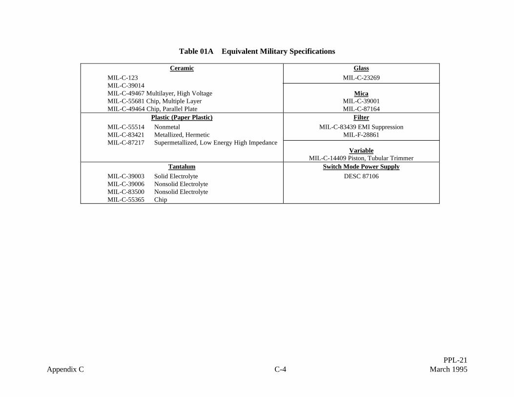
PPL-21Appendix C C-4 March 1995
Table 01A Equivalent Military Specifications
CeramicMIL-C-123MIL-C-39014MIL-C-49467 Multilayer, High VoltageMIL-C-55681 Chip, Multiple LayerMIL-C-49464 Chip, Parallel Plate
GlassMIL-C-23269
MicaMIL-C-39001MIL-C-87164
Plastic (Paper Plastic)MIL-C-55514 NonmetalMIL-C-83421 Metallized, HermeticMIL-C-87217 Supermetallized, Low Energy High Impedance
FilterMIL-C-83439 EMI Suppression
MIL-F-28861
VariableMIL-C-14409 Piston, Tubular Trimmer
TantalumMIL-C-39003 Solid ElectrolyteMIL-C-39006 Nonsolid ElectrolyteMIL-C-83500 Nonsolid ElectrolyteMIL-C-55365 Chip
Switch Mode Power SupplyDESC 87106

Notice 1PPL-21
Appendix C C-5 May 1996
Table 02 Connector Screening Requirements (Notes 1, 2) (Page 1 of 7)
Test Methods, Connector Type/Grade LevelInspection/ Conditions and Circular D-Subminiature Microminiature Printed Circuit
Test Requirements 1 2 1 2 1 2 1 2Visual Inspection Verify proper marking, free of
workmanship defects in accordancewith Table 02A. 3X magnification(min.) and high intensity lighting.
X X X X X X X X
Mechanical Inspection Verify design, construction,dimensions, materials and finish.
X 2 (0) X 2 (0) X 2 (0) X 2 (0)
Dielectric Withstanding Voltage(Sea Level)
MIL-STD-1344, Method 3001.Refer to reference specifications forvoltages, mating requirements.
X 2 (0) X 2 (0) X X X 2 (0)
Insulation Resistance MIL-STD-1344, Method 3003,Condition B. 5000 megohms min. inaccordance with referencespecifications.
X 2 (0) X 2 (0) X 2 (0) X 2 (0)
Outgassing Control (As req’d) (Note 4) X X X X X XContact engagement andseparation force. (non-removable socket contacts)
MIL-STD-1344, Method 2014,MIL-C-83513, Paragraph 4.7.8 formicrominiature connectors. (Note 5)
2 (0) 2 (0) 2 (0) 2 (0)2 (0) 2 (0)
2 (0) 2 (0)
Thermal shock (liquid to liquid,hermetic receptacles only)
MIL-C-38999, paragraph 4.7.3. Tencycles from 4°C max to 90°C min.Transfer time shall not exceed 5seconds. Dwell time shall be 10minutes, min at each extreme.
X 2 (0)
Hermeticity(Sealed Receptacles Only)
MIL-STD-1344, Method 1008,Pressure differential across theconnector shall be 1 atmosphere (14.7PSI). Leakage shall not exceed1x10-7 ATM CM3/Sec or as otherwisespecified.
X 2 (0) X 2 (0)
See notes on page C-9.
(Note 3)(Note 3)

Notice 1PPL-21
Appendix C C-6 May 1996
Table 02 Connector Screening Requirements (Notes 1, 2) (Page 2 of 7)
Test Methods, Connector Type/Grade LevelInspection/ Conditions and Circular D-Subminiature Microminiature Printed Circuit
Test Requirements 1 2 1 2 1 2 1 2Contact Retention MIL-STD-1344, Method 2007. Apply
load per reference specification.2 (0) 2 (0) 2 (0) 2 (0) 2 (0) 2 (0) 2 (0) 2 (0)
Residual Magnetism (Nonmagnetic Connectors andContacts)
S-311-P-4, Paragraph 4.5.1 orS-311-P-10, Paragraph 4.5.5
X X
Mating and Unmating Force MIL-STD-1314, Method 2013 2 (0) 2 (0) 2 (0) 2 (0)MIL-C-55302, Paragraph 4.7.4. Forceshall be per reference specification xno. of contacts.
2 (0) 2 (0)
Low Level Signal ContactResistance (Note 8)
MIL-STD-1344 Method 3002 X 2 (0) X 2 (0)
Resistance to Soldering Heat(Note 9)
MIL-C-24308, Paragraph 4.7.2.6MIL-C-83513, Paragraph 4.7.11MIL-STD-202, Method 210,Condition C
2 (0) 2 (0)2 (0) 2 (0)
2 (0) 2 (0)
See notes on page C-9.
(Note 6)(Note 6)
(Note 7)(Note 7)

Notice 1PPL-21
Appendix C C-7 May 1996
Table 02 Connector Screening Requirements (Notes 1, 2) (Page 3 of 7)
Test Methods, Connector Type/Grade LevelInspection/ Conditions and Radio Frequency Contacts EMI Filter Pin High Voltage
Test Requirements 1 2 1 2 1 2 1 2Visual Inspection Verify proper marking, free of
workmanship defects in accordancewith Table 02A. 3X magnification(min.) and high intensity lighting.
X X X X X X X X
Mechanical Inspection Verify design, construction,dimensions, materials and finish.
X 2 (0) X 2 (0) X 1(0) X 2 (0)
Dielectric Withstanding Voltage(Sea Level)
MIL-STD-1344, Method 3001.MIL-STD-202, Method 301 for RFconnectors. Refer to referencespecifications for voltages, matingrequirements.
2 (0)2 (0) X X X X X
Insulation Resistance MIL-STD-202, Method 302 for RFconnectors and filter pins. 5000megohms min. in accordance withreference specifications.
2 (0) X X
Outgassing Control(As required)
(Note 4) X X X X X X X X
Contact engagement andseparation force.
MIL-STD-1344, Method 2014. X X
Hermeticity(Sealed Receptacles Only)
MIL-STD-202, Method 112, ConditionC, Procedure III. Pressure as specified.
X 2 (0)
Contact Retention MIL-C-39012, Paragraph 4.6.9. Applyload per reference specification.
2 (0) 2 (0)
See notes on page C-9.
(Note 13)(Note 13)(Note 12)(Note 12)(Note 11)(Note 11)(Note 10)
(Note 14) (Note 14)
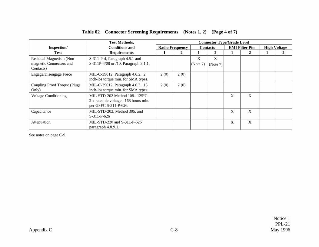
Notice 1PPL-21
Appendix C C-8 May 1996
Table 02 Connector Screening Requirements (Notes 1, 2) (Page 4 of 7)
Test Methods, Connector Type/Grade LevelInspection/ Conditions and Radio Frequency Contacts EMI Filter Pin High Voltage
Test Requirements 1 2 1 2 1 2 1 2Residual Magnetism (Nonmagnetic Connectors andContacts)
S-311-P-4, Paragraph 4.5.1 andS-311P-4/08 or /10, Paragraph 3.1.1.
X X
Engage/Disengage Force MIL-C-39012, Paragraph 4.6.2. 2inch-lbs torque min. for SMA types.
2 (0) 2 (0)
Coupling Proof Torque (PlugsOnly)
MIL-C-39012, Paragraph 4.6.3. 15inch-lbs torque min. for SMA types.
2 (0) 2 (0)
Voltage Conditioning MIL-STD-202 Method 108. 125°C.2 x rated dc voltage. 168 hours min.per GSFC S-311-P-626.
X X
Capacitance MIL-STD-202, Method 305, andS-311-P-626
X X
Attenuation MIL-STD-220 and S-311-P-626paragraph 4.8.9.1.
X X
See notes on page C-9.
(Note 7)(Note 7)

Notice 1PPL-21
Appendix C C-9 May 1996
Table 02 Connector Screening Requirements (Page 5 of 7)
Notes:1. For commercial connectors procured from a manufacturer who is listed on the QPL for a similar connector, screening tests do not have to be repeated if
attributes data or a certificate of compliance is acquired from the manufacturer, and indicate that the tests were performed. However, sample testing cannever be a substitute for 100% testing. 100% examination may be performed at the user’s receiving and inspection facilities in lieu of performance by themanufacturer.
2. An “X” in the table indicates that the inspection/test is to be performed on a 100% basis. Y (0) indicates the quantity (accept number) for sample testing.If a failure occurs during sample testing, the tests shall either be performed on a 100% basis or the sample size shall be tripled and the tests repeated. If afailure occurs during the second sample test, the lot shall be rejected.
3. For MIL-C-83513 microminiature connectors with crimp type pig tail leads, adjacent leads shall be tested for shorting prior to DWV. Each lead shall betested. For DWV testing, a test potential of 600 VRMS (sea level) shall be used. If manufacturer can certify that this test is performed on each connector,additional testing is not required.
4. All non metallic materials shall be traceable to acceptable outgassing test results in NASA reference publication 1124 or MSFC-HDBK-527.
a. Some QPL manufacturers provide circular connectors which are specially processed to meet outgassing requirements, indicated by a special suffix tothe commercial equivalent of the military part number. The user may process connectors for outgassing control by removing and replacing lubricantwith a low outgassing lubricant followed by a bakeout of 24 hours at 125°C. Low outgassing lubricants as well as other acceptable variations ofbakeout time, temperature, and vacuum for outgassing control are contained in NASA Reference publication 1124. Since removal and replacement oflubricant requires disassembly and is labor intensive, it is recommended that this processing be performed by the manufacturer to a controlledspecification.
b. Some commercial D-Subminiature connectors contain a rear silicone rubber sealing grommet behind the connector which provides wire support andseals the rear of the connector, but represents an outgassing concern. A bakeout of 125°C for 24 hours is recommended for outgassing control.
c. Microminiature receptacles contain either a fluorosilicone (acceptable) or silicone rubber interface seal. The silicone rubber seal may be an outgassingconcern and can be carefully removed with small tweezers and discarded. Otherwise, a bakeout of 24 hours at 125°C is recommended.
d. Type SMA RF connector plugs may contain a silicone rubber O-Ring interface seal inside the coupling nut, on the mounting flange or inside the cablenut, and require replacement with fluorosilicone O-Rings or a 125°C bakeout for 24 hours to prevent outgassing.
e. High voltage panel mount receptacle connectors contain a small silicone rubber grommet which surrounds the center pin contact. This grommet is anoutgassing concern, and a bakeout of 125°C is recommended for outgassing control.

Notice 1PPL-21
Appendix C C-10 May 1996
Table 02 Connector Screening Requirements (Page 6 of 7)
Notes (Continued):5. a. Circular connectors. Applies to nonremovable solder socket contacts only. In-process inspections shall be used. MS3197 test pin shall be inserted to
.7L and measured forces shall comply with MIL-C-39029, Table IX. All socket contacts shall be measured for acceptable levels of separation force.Ten percent of contacts selected at random shall be measured for insertion force.
b. D-Subminiature connectors. Applies to nonremovable solder socket contacts. Insert and remove maximum diameter MS3197 gage pin. Insertminimum diameter gage pin, and measure separation force. Insert and separate maximum diameter gage pin three times, and measure engagementforce during third cycle. All measurements shall comply with MIL-C-39029, Table IX. Test 20 percent of contacts (min of four) from each sample.
c. Microminiature connectors. Twenty percent of pin contacts (min of seven) per test sample shall be tested using socket test sleeves per MIL-C-83513.Engagement force shall be 6 ounces maximum per contact. Separation force shall be 0.5 ounces minimum per contact.
d. Printed Circuit Connectors. In process testing shall be used. Applies to socket contacts only. Insert MS3197 test pins to a depth of .140 inches.Maximum engagement force shall be 12 ounces per contact for standard force contacts and 4 ounces per contact for low insertion force contacts.Minimum separation force is 5 ounces per contact (each type). Sample size shall be per MIL-STD-105, general inspection level II, .65% AQL.
6. For MIL-C-83513 microminature connectors with crimp type pigtail leads, apply a 5 lb. load to individual wire pigtails for 6 seconds, minimum. Loadshall not displace contact or pull the wire from the crimp contact.
7. When low residual magnetism is a requirement, each connector must be tested for specific levels of residual magnetism. The test procedure in GSFCS-311-P-4, Paragraph 4.5.1 or S-311-P-10, Paragraph 4.5.5 shall apply. The test procedure in GSFC S-311-P-4/08 and /10 paragraph 3.3.1 shall apply forcontacts. Contacts shall be grouped together and the measured value for the group shall not exceed a gamma level of 0.1 x the number of contacts in thegroup. Following testing, connectors and contacts shall be demagnetized per S-311-P-4 paragraph 6.1.3 or equivalent. Performance of residualmagnetism requires the use of specialized test equipment and should be performed at the manufacturer’s facilities.
8. Test is intended to determine resistance of contacts with crimp joined or weld joined solid straight or formed wire leads. Test shall be performed using amicro-ohmmeter and four wire measurements. Mated connector pairs are preferred. Attached current leads at extreme ends of contacts. Attach voltageleads at contact lead closest point to engagement barrel without touching barrel. Apply one milliamp DC or as otherwise specified. Measurement shall notexceed 15 milliohms for size 22 contacts, 20 milliohms for size 24 contacts, 32 milliohms for size 26 contacts, or as otherwise specified.
9. Test is not required for connectors with diallyl phthalate insert material. For connectors with thermoplastic insert material, test 20% of contacts(7 minimum). Solder cup contacts or PC terminations shall be soldered with a pencil type iron heated to 360°C using SN63 solder for a minimumduration of four seconds. There shall be no evidence of damage or distortion. Contact floating conditions, if applicable, shall be maintained.
10. For coaxial connectors, the connector shall be terminated to the appropriate coaxial cable, and the applied voltage shall be as specified in the detailspecification.
11. For coaxial contacts, the dielectric withstanding voltage test shall be performed in accordance with MIL-STD-1344, Method 3001. A voltage of 1000VRMS (Sea Level) shall be applied for 10 seconds between inner contact and shell.

Notice 1PPL-21
Appendix C C-11 May 1996
Table 02 Connector Screening Requirements (Page 7 of 7)
Notes (Continued):12. For filter pin connectors, dielectric withstanding voltage of twice the rated dc voltage shall be applied for five to ten seconds between each contact and the
shell. Current shall be limited to 20 milliamps.
13. High voltage connectors have voltage ratings in excess of 5KV and are similar to Reynolds part numbers 167-3770 and 167-3771. For high voltageconnectors rated at 10KVDC, a potential of 15KVDC shall be applied to each connector for 10 seconds, minimum.
14. Applies to sockets only. For both contact engagement force and contact separation force, engage contact with MS3197 test pin to a depth of 0.7L. Forceshall comply with MIL-C-39029, Table IX. For sizes 16 and smaller, each contact shall be tested for separation force. MIL-STD-105, general inspectionlevel II, 1% AQL shall apply for larger contact sizes and for insertion force.

Notice 1PPL-21
Appendix C C-12 May 1996
Table 02A Inspection Criteria for Connectors and Contacts (Note 1)
DEFECT Circulars DSUBSMicro-
miniature PC RF ContactsRF
ContactsFilterPin
HighVoltage
INSERTInsert to Shell Positioning andOrientationCracks, ChipsMarkingNegative Meniscus of Glass
(Hermetics only-glass to contact andglass to shell)
GROMMETNicks, Gougles, Tears, FoldsMarking
SHELLSCracks, Dents, ScratchesFinish (Peeled or blistered plating, discoloration, exposed base metal)Marking Completeness, LegibilitySleeves (Fixed - Not free to move)
THREADS (As Applicable)Nicks, Dents, Voids
ADHESIVESExcess Bonding Material (Overflow)Voids
XXXX
X
XXX
XXX
X
XX
XXX
XXX
X
XXX
X
XXX
XXX
X
XXX
X
XXX
X
XX
XXX
XXX
X
XXX
X
XX
XXX
XXX
XX
XXX
XXX
XX
XXXX
XXX
X
XXX
XXX
XX
XXX
XX
XXX

PPL-21Appendix C C-13 March 1995
Table 03 Filter Screening Requirements
Inspection/Test Test Methods Conditions, and Grade 1 Grade 2
Requirements Reference MIL-F-28861
1) Visual Inspection Elements and subassemblies in accordance withparagraph 4.6.1.2
X X
2) External Visual Dimensions, marking, workmanship X X 3) Thermal Shock MIL-STD- 202, Method 107 Condition A
except step 3 shall be 125°CX
(Note 1)X
4) Voltage Conditioning (Burn-In) Duration (Hours)
MIL-STD-202, Method 108, 125°±3°C. 2 xrated voltage for dc rated. 1.2 x rated ac voltageat max. rated frequency for ac, ac/dc rated
X(Note 2)
240
X
160 5) Insulation Resistance or DC
Leakage CurrentMIL-STD-202, Method 302, rated dc voltageapplied for 2 minutes max., charging current of50 mA max.
X(Note 3)
X(Note 3)
6) Capacitance to ground MIL-STD-202, Method 305, 1.0±.2V RMS.1 Mhz ±100khz for capacitors ≤100pF. 1khz±100Hz for Capacitors ≥100pF
X X
7) Dissipation factor Frequency and voltage specified in 6) above.Accuracy shall be ± 2 percent.
X X
8) Insertion Loss MIL-STD-220 and paragraph 4.6.5 X X 9) Voltage Drop ac and dc. Paragraph 4.6.6 X X10) Radiographic Inspection MIL-STD-202, Method 209 and paragraph
4.6.8X
11) Seal Test (Hermetic types only)Gross LeakFine Leak
MIL-STD-202, Method 112Condition A or BCondition C
XX
X
Notes:1. Grade 1 filters shall be torqued in place and insulation resistance measured at 125°C before removing filter from plate.2. Polarity shall be reversed from first 24 to 72 hours. Refer to paragraph 4.6.2.2.2 and Figure 1 for test circuit.3. Shall be measured within 1 hour after voltage conditioning.

Notice 1PPL-21
Appendix C C-14 March 1995
Table 04 Fuse Screening Requirements
Inspection/Test Test Methods, Conditions, and Requirements Notes Part Type/Grade Level
(Note 1) 1 2
Visual Inspections Materials, design, construction, marking, andworkmanship X X
Mechanical Inspections Body and lead dimensions to specification 2 X XResistance (Cold) MIL-STD-202, Method 303
Resistance to specification 3 X X
Voltage Drop (Hot-1) 100% rated current for 5 minutes (minimum)Voltage drop to specification (when specified) 4 X X
Thermal Shock MIL-STD-202, Method 107Condition B 5, 6 X X
Voltage Drop (Hot-2) 100% rated current for 5 minutes (minimum)Ratio voltage drop:
(Hot-1/Hot-2) = 0.97 to 1.03X X
Resistance (Cold) MIL-STD-202, Method 303Resistance to specification 3 X X
Seal MIL-STD-202, Method 112Test Condition A X X
Percent Defective Allowable(PDA)
Grade 1- 5%Grade 2- 10% 7 X X
Notes:1. It is the responsibility of the user to specify the test conditions and define the pass/fail criteria for each inspection. These values shall be based on the
nearest equivalent military specification, the manufacturer’s specification, or the application, whichever is most severe.2. A minimum of three fuses shall be measured. In the event of failure, the entire lot shall be screened for dimensions and rejects discarded.3. The source current for the resistance measurement shall not exceed 10% of the nominal current rating at room temperature.4. The voltage drop (hot ) measurement must be recorded to calculate the voltage drop ratio regardless of whether or not it is a specification requirement.5. Fuses rated < +125°C shall be tested to Condition A.6. External visual examination is required after testing to verify no evidence of mechanical damage.7. Marking and voltage ratio rejects shall not be counted for purposes of establishing the defect rate.

PPL-21Appendix C C-15 March 1995
Table 05 Coil/Inductor Screening Requirements
Part Type (Note 2)
Test Methods and ConditionsGroup 1Grade
Group 2Grade
Group 3Grade
Testing (Note 1) 1 2 1 2 1 2Thermal Shock25 Cycles10 Cycles
MIL-STD-202, Method 107Continually monitor during final cycle to verifyno intermittent conditions in accordance withMIL-STD-981 (Note 3)
XX
X X X X
No Load Burn-In 96 hrs. at max. rated temperature. No voltageapplied.
X X X X X X
Seal (if applicable) MIL-T-27 Paragraph 4.8.7 X XD W V MIL-STD-202, Methods 301 and 105 (Note 4) X X X X X XQ X X X XSelf Resonant Frequency X X X XInsulation Resistance MIL-STD-202 Method 302, 500V dc or as
SpecifiedX X X X X X
Inductance X X X X X XDC Resistance X X X X X XRadiographic MIL-STD-981 Appendix C X X XVisual X X X X X X
Notes:1. Test methods not specified herein shall be in accordance with MIL-T-27, MIL-C-15305, and MIL-C-83446 for Group 1, 2, and 3 inductors respectively.2. Group 1 includes power, audio, charging, and saturable inductors (families 04, 20, 37 and 41 respectively). Group 2 includes radio frequency, fixed and
variable coils (families 13 and 14 respectively). Group 3 includes radio frequency, chip fixed, and variable coils (families 50 and 51 respectively).3. For grade 1 parts with magnet wire less than 30 AWG, measure DC resistance before and after thermal shocks. The resistance charge shall not exceed +3
percent.4. Dielectric withstanding voltage shall be measured at sea level and at high altitude. Test voltage and conditions shall be specified.

Notice 1PPL-21
Appendix C C-16 May 1996
Table 06 Relay Screening Requirements (Page 1 of 3) (Notes 1, 2)
Test Methods, Conditions and Part Type/Grade LevelInspection/Test Requirements (Note 3) Notes 1 2
Cleaning and Small ParticleInspection Manufacturer’s approved procedure 4 X X
Visual Inspection (External) Materials, design, construction, header glass, marking, andworkmanship 5 X X
Mechanical Inspections Critical physical dimensions 6 X XInitial Electrical Inspections Table 06A XVibrational Scan (Sinusoidal) MIL-STD-202, Method 204
Specified test condition (amplitude, frequency range, sweep time andduration)
Specified electrical load conditionsSpecified contact loadContact monitoring to specificationContact transfer to specification
7, 8,9, 10
X X
PIND Manufacturer’s approved procedure 11 X XInternal Moisture Detection Relay dwell with coils deenergized for 30 minutes at 20±5°C
IR ≥ 10,000 megohms (between all contact pins together and case)Energize relay coil at 140% rated voltage for 2.5 minutes. Repeat for
two-coil latching relays.IR ≥ 10,000 megohms (between all contact pins together and case)
X X
High Temperature Soak 16 hours at maximum rated operating temperatureEnergize coil at 120% rated voltage. For two coil latching relays,
alternately energize coils 4 hours at a time.X X
Run-In Tests Low temperature run-in1 hour dwell at minimum rated operating temperaturePickup or latch/reset voltage to specificationContact loading: open circuit load voltage at 10 to 50 µV
load current at 10 to 50µACycling rate: 60 actuations/minute (minimum)Specified number of cycles
Grade 1 - 2500 cyclesGrade 2 - 2500 cycles
Miss level: 100 ohms maximum
12
X X
See notes on page C-18.

Notice 1PPL-21
Appendix C C-17 May 1996
Table 06 Relay Screening Requirements (Page 2 of 3) (Notes 1, 2)Test Methods, Conditions and Part Type/Grade Level
Inspection/Test Requirements (Note 3) Notes 1 2Run-In Tests (continued) High temperature run-in
Rated coil voltage for 1 hour at maximum rated operating temperatureFor two-coil latching relays, 30 minutes each coilPickup or latch/reset voltage to specificationContact loading: open circuit load voltage at 10 to 50 µV
load current at 10 to 50µACycling rate: 60 actuations/minute (minimum)Specified number of cycles
Grade 1 - 2500 cyclesGrade 2 - 2500 cycles
Miss level: 100 ohms maximumRoom temperature run-in1 hour dwell at 25±5°CPickup or latch/reset voltage to specificationContact loading: open circuit load voltage at 10 to 50 µV
load current at 10 to 50µACycling rate: 60 actuations/minute (minimum)Specified number of cycles
Grade 1 - 2500 cyclesMiss level: 100 ohms maximum
X
X
X
Radiographic Inspection MSFC-STD-355C XHermetic Seal Fine leak: MIL-STD-202, Method 112
Test Condition C1.0 X 10-8 cc/sec.orMIL-STD-883, Method 1014Test Condition A1, A2, or B1.0 X 10-8 cc/sec.
Gross Leak: MIL-STD-883, Method 1014Condition D
X X
Final Electrical Inspections Table 06A 13 X XPercent Defective Allowable (PDA) Grade 1- 5%
Grade 2- 10% 13 X X
See notes on page C-18.

Notice 1PPL-21
Appendix C C-18 May 1996
Table 06 Relay Screening Requirements (Page 3 of 3) (Notes 1, 2)
Notes:1 This screening table is suitable for both low level and high level relays, latching and nonlatching. Unless otherwise specif ied, relays with dc resistive
contact ratings up to and including 2 amperes shall be considered low level relays. Relays with dc resistive contact ratings higher than 2 amperes shall beconsidered high level relays.
2. Screening in accordance with MIL-R-39016, MIL-R-6106, MIL-R-83536, or GSFC S-311-P-754 is acceptable in lieu of the screening specified in thistable for Grade 2.
3. It is the responsibility of the user to specify the test conditions and define the pass/fail criteria for each inspection. These values shall be based on thenearest equivalent military specification, the manufacturer’s specification, or the application, whichever is most severe.
4. It is the responsibility of the user to approve manufacturer procedures for internal visual inspection and cleaning of relays prior to canning. Appendix A toMIL-R-83536 may be used as a guideline. These procedures must be documented, on file at the user’s facility, and available for NASA review. TheNASA/GSFC Parts Branch (Code 311) maintains a list of relay manufacturer approved procedures.
5. Header glass inspection shall be performed with microscopic power of at least 10X and shall include examinations for the following types of irregularities:blisters, foreign material, dark spots, cracks and chips. Meniscuses shall not extend up the terminal more than 0.20 inch or one-third the terminaldiameter, whichever is greater.
6. A minimum of 3 relays shall be measured. In the event of a failure, the entire lot shall be screened for dimensions and rejects discarded.7. All relays shall be vibrated in the direction of contact motion.8. Contacts shall be monitored with an adequate test circuit to verify that no opening of closed contacts in excess of 10 microseconds, nor closing of open
contacts in excess of 1 microsecond, occurs. The contact load shall be 10 mA maximum at 6 Vdc maximum.9. Prior to removal from the test fixture, apply maximum over the temperature range pickup or latching voltage to the coil and verify that relay contacts have
switched. Remove pickup voltage or apply reset voltage and verify that contacts have switched again. Failure of relay contacts to transfer in eitherdirection shall be cause for rejection.
10. External visual examination required after testing to verify no evidence of mechanical damage.11. It is the responsibility of the user to approve manufacturer procedures for particle impact noise detection (PIND). Appendix B to MIL-R-83536 may be
used as a guideline. These procedures must be documented, on file at the user’s facility, and available for NASA review. The NASA/GSFC Parts Branch(Code 311) maintains a list of relay manufacturer approved procedures for PIND testing.
12. The specified sequence (low temperature, high temperature, room temperature) is preferred. However, it is acceptable to perform the high temperaturerun-in prior to the low temperature run-in.
13. Only the final electrical inspection results shall be used to determine the defect rate for the PDA.

Notice 1PPL-21
Appendix C C-19 May 1996
Table 06A Relay Electrical Inspections (Page 1 of 4) (Note 1)
Test Methods, Conditions and Part Type/Grade LevelInspection/Test Requirements (Note 2) Notes 1 2
DC Coil Resistance MIL-STD-202, Method 303 X XStatic Contact Resistance
or
Contact Voltage Drop
Low level relaysMIL-STD-202, Method 307Test load: 10 mA maximum at 6 V maximum (dc or peak ac)No actuations prior to measurementMeasurements between all contact pairsOne measurement for each of three actuations (use average value)Static contact resistance to specification
High level relaysMIL-STD-202, Method 307Test load: rated dc resistive contact current at 6 V maximum (dc or
peak ac)No actuations prior to measurementMeasurements between all contact pairsOne measurement for each of ten actuations (use average value)Contact voltage drop to specification
X X
Pickup, Hold, and Dropout Voltages
or
Latch/Reset Voltages
Nonlatching relaysGradually step or ramp coil voltage until the relay contacts switchPickup voltage to specificationGradually reduce coil voltage to specified hold voltageNo switching of contactsGradually reduce coil voltage until contacts switch to their original stateDropout voltage to specification
Latching relaysGradually step or ramp latch coil voltage until the relay contacts switchLatch voltage to specificationRemove latching voltageGradually step or ramp reset coil voltage until the relay contacts switchReset voltage to specification
3 X X
See notes on page C-21.

Notice 1PPL-21
Appendix C C-20 May 1996
Table 06A Relay Electrical Inspections (Page 2 of 4) (Note 1)
Test Methods, Conditions and Part Type/Grade LevelInspection/Test Requirements (Note 2) Notes 1 2
Operate and Release Time Use oscilloscope or other acceptable means to time each pair of contactsMeasurements shall be exclusive of bounce or stabilization timesContact load: 10 mA maximum at 6 V maximum (dc or peak ac)Alternately apply and remove rated coil voltage a total of 5 timesOperate and release time to specification based on the average of 5
consecutive measurements
4 X X
Contact Bounce Time Use oscilloscope or other acceptable means to time each pair of contactsContact load: 10 mA maximum at 6 V maximum (dc or peak ac)Alternately apply and remove rated coil voltage a total of 5 timesContact bounce time to specification based on the average of 5
consecutive measurements
5 X X
Contact Stabilization Time(when specified)
Use oscilloscope or other acceptable means to time each pair of contactsContact load: 50 mA maximum at 50 mV maximum (dc or peak ac)Alternately apply and remove rated coil voltage a total of 5 timesContact stabilization time to specification based on the average of 5
consecutive measurements
6 X X
Dielectric Withstanding Voltage MIL-STD-202, Method 301Specified test voltageLeakage current to specification
7, 8, 9 X X
Insulation Resistance MIL-STD-202, Method 302Test Condition A (relays with coil and contact ratings both < 60 volts)Test Condition B (other relays)Resistance (minimum) to specification
8 X X
Coil Transient Suppression Use oscilloscope or other acceptable means to observe magnitude of theinduced voltage transient across the coil(s)
Rated coil voltageThe maximum of three consecutive readings shall be recordedBack EMF (induced voltage) to specification
10 X X
See notes on page C-21.

Notice 1PPL-21
Appendix C C-21 May 1996
Table 06A Relay Electrical Inspections (Page 3 of 4) (Note 1)
Test Methods, Conditions and Part Type/Grade LevelInspection/Test Requirements (Note 2) Notes 1 2
Neutral Screen Rated coil voltage to both coils simultaneously for a period of 10milliseconds minimum
Repeat three timesNeutral screen to specificationIn the event of failure, apply a 10±1 ms pulse at maximum allowable
latch voltage (at 25°C)Latch to specificationApply 10±1 ms pulse at maximum allowable reset voltage (at 25°C)Reset to specification
11, 12 X X
Non-Make-Before-Break Rated pickup, latch or reset voltageContact load: 10 mA maximum at 6 V maximum (dc or ac peak)Energize and deenergize 10 consecutive cyclesNon-make-before-break to specification
X X
Notes:1. This table is suitable for both low level and high level relays, latching and nonlatching. Unless otherwise specified, relays with dc resistive contact ratings
up to and including 2 amperes shall be considered low level relays. Relays with dc resistive contact ratings higher than 2 amperes shall be considered highlevel relays.
2. It is the responsibility of the user to specify the test conditions and define the pass/fail criteria for each inspection. These values shall be based on thenearest equivalent military specification, the manufacturer’s specification, or the application, whichever is most severe.
3. For screening, the mounting position of the relay is optional.4. Release time is not applicable to latching relays.5. A contact bounce shall be considered any occurrence equal to or greater than 90 percent of the open circuit voltage with a pulse width of 10 microseconds
or greater. Lesser values are considered to be dynamic contact resistance.6. Contact stabilization time is the maximum time allowed for the contacts to reach and maintain a static contact resistance state following the actual operate
or release time of the relay. Essentially, it is the sum of the contact bounce time plus the time required for the dynamic contact resistance to stabilize tostatic contact resistance.
7. The DWV test duration shall be 5 seconds minimum.8. Points of application for testing: (1) between case, frame or enclosure, and between all contacts in the energized and deenergized positions; (2) between
case, frame or enclosure and coil(s); (3) between all contacts and coil(s); (4) between open contacts in the energized and deenergized positions; (5)between coils of dual-coil relays; (6) and between contact poles in the energized and deenergized positions.

Notice 1PPL-21
Appendix C C-22 May 1996
Table 06A Relay Electrical Inspections (Page 4 of 4)
Notes (Continued):9. External visual examination required after testing to verify no evidence of mechanical damage.10. Applicable only to dc operated relays with diodes for coil transient voltage suppression.11. Applicable only to latching relays.12. A relay which will not assume a neutral position for three successive test cycles is considered an acceptable part and does not require further testing.

PPL-21Appendix C C-23 March 1995
Table 07 Fixed Resistor Screening Requirements (Page 1 of 2)
Part Type/Grade LevelInspection/Test Test Methods, Conditions and
Requirements (Note 1)Notes
Composition Film Wirewound1 2 1 2 1 2
Precap Visual Inspection Networks: Particles, metallization (scratches,voids, adherence, bridging, alignment,corrosion, probe marks), laser trim faults,bonding pad defects, oxide defects
Others: Not applicable
2, 3 X
Visual Inspections Materials, design, construction, marking, andworkmanship 4 X X X X X X
Mechanical Inspections Critical physical dimensions 5 X X X X X XInitial dc Resistance MIL-STD-202, Method 303 6, 7, 8 X X X X X XThermal Shock MIL-STD-202, Method 107
Grade 1 - 25 cyclesGrade 2 - 10 cycles
High temperature - max. rated operatingLow temperature - min. rated operating
9, 10 X X
Power Conditioning MIL-STD-202, Method 108
Specified rated wattage multipleSpecified temperatureSpecified time
If time ≤ 24 hours: continuous operationIf time > 24 hours: 1.5 hours on, 0.5 hours off
9, 1011, 12
X X X X
Final dc Resistance MIL-STD-202, Method 303Resistance and ∆R to specification
X X
See notes on page C-24.

PPL-21Appendix C C-24 March 1995
Table 07 Fixed Resistor Screening Requirements (Page 2 of 2)
Part Type/Grade LevelInspection/Test Test Methods, Conditions and
Requirements (Note 1)Notes
Composition Film Wirewound1 2 1 2 1 2
Hermetic Seal Fine leak: MIL-STD-202, Method 112Test Condition C5.0 X 10-7 cc/sec. (networks)1.0 X 10⁻⁸ cc/sec. (others)
Gross Leak: MIL-STD-883, Method 1014Condition D
13 X X
Radiographic Inspection MSFC-STD-355C 14 X XPercent DefectiveAllowable (PDA)
Grade 1 - 5%Grade 2 -10% 15 X X X X X X
Notes:1. It is the responsibility of the user to specify the test conditions and define the pass/fail criteria for each inspection. These values shall be based on the
nearest equivalent military specification, the manufacturer’s specification, or the application, whichever is most severe.2. Examination shall be performed using binocular magnification of 50X to 100X.3. If solder is used for internal connections, it shall have a liquid point not less than +280°C.4. Small resistors, such as chip resistors, shall be examined using 30X to 60X magnification, but in case of conflict, 30X shall be the referee power.5. A minimum of 3 resistors shall be measured. In the event of a failure, the entire lot shall be screened for dimensions and rejects discarded.6. The test voltage must be specified in the SCD or by the manufacturer (commercial parts).7. For networks, unless otherwise specified, individual resistive elements shall be isolated (whenever possible) to minimize computation of pin-to-pin
resistance values.8. Out of tolerance composition resistors shall be baked in accordance with the SCD or manufacturer's instructions and then remeasured. Resistors that
remain out of tolerance after baking shall be considered failures.9. ∆R is optional after this inspection if ∆R is specified for thermal shock and conditioning combined.10. External visual examination required after testing to verify no evidence of mechanical damage.11. Not applicable to chip resistors. Conditioning time for film networks with internal solder terminations shall be 250 hours minimum.12. Unless otherwise specified, the manufacturer's maximum rated continuous dc working voltage should not be exceeded during conditioning as determined
by V = √PR.13. Applicable only to hermetically sealed networks and high stability film resistors.14. Not applicable to composition, chip or network resistors.15. Marking and cosmetic defects shall not be counted for purposes of establishing the defect rate for PDA.

PPL-21Appendix C C-25 March 1995
Table 07A Variable Resistor Screening Requirements (Page 1 of 3)
Part Type/Grade LevelInspection/Test Test Methods, Conditions and Requirements (Note 1) Notes Non-Wirewound Wirewound
1 2 1 2Visual Inspections Materials, design, construction, marking, and workmanship X X X XMechanical Inspections Critical physical dimensions 2 X X X XThermal Shock MIL-STD-202, Method 107
Grade 1 - 25 cyclesGrade 2 - 10 cycles
High temperature - max. rated operatingLow temperature - min. rated operating
Total resistance and ∆R to specificationSetting stability (∆%) to specificationContinuity check
3, 4, 5, 6 X X X X
Conditioning MIL-STD-202, Method 108
Specified rated wattage multipleSpecified temperature100 hours minimum (Grade 1), 1.5 hours on, 0.5 hours off 50 hours minimum (Grade 2), 1.5 hours on, 0.5 hours off
Total resistance and ∆R to specification
3, 4, 7 X X X X
Contact ResistanceVariation or Peak Noise
Contact resistance variation to specification, orPeak noise (resistance variation) to specification 8 X X X X
Immersion Gross leak: MIL-STD-202, Method 112, Test Condition D
Modify as follows:1. Precondition resistors at +125°C for 15±2 minutes.2. Stabilize at room temperature for 15±2 minutes.3. Immerse into fluorocarbon bath held at +85°C to +90°C,
shake for 5 seconds maximum, then keep resistorssubmerged for a period of 1 minute ±5 seconds.
4. Discard resistors with inadequate seals as evidenced by acontinuous stream of bubbles emanating from anyconcentrated point on the resistor.
X X X X
See notes on page C-26.

PPL-21Appendix C C-26 March 1995
Table 07A Variable Resistor Screening Requirements (Page 2 of 3)
Part Type/Grade LevelInspection/Test Test Methods, Conditions and Requirements (Note 1) Notes
Non-Wirewound Wirewound1 2 1 2
Actual EffectiveElectrical Travel Number of turns or angular degrees to specification 9 X X
Absolute MinimumResistance Resistance to specification 10 X X
End Resistance Resistance to specification 11 X X X XDWV MIL-STD-202, Method 301
Specified test voltageBetween terminals tied together and all external metal portionsLeakage current to specification
3 X X
IR MIL-STD-202, Method 302, Test Condition A or BBetween terminals tied together and all external metal portionsResistance (minimum) to specification
X X
Torque Operating torque to specificationClutch to specification (when applicable)Stop strength to specification (when applicable)
12, 13, 14 X X X X
Radiographic Inspection MIL-STD-202, Method 209 15 X XPercent DefectiveAllowable (PDA)
Grade 1 - 5%Grade 2 -10% 16 X X X X
Notes:1. It is the responsibility of the user to specify the test conditions and define the pass/fail criteria for each inspection. These values shall be based on the
nearest equivalent military specification, the manufacturer’s specification, or the application, whichever is most severe.2. A minimum of 3 resistors shall be measured. In the event of a failure, the entire lot shall be screened for dimensions and rejects discarded.3. External visual examination required after testing to verify no evidence of mechanical damage.4. Total resistance shall be measured between the end terminals with the movable contact arm positioned against a stop. The positioning of the contact arm
and terminal shall be the same for all subsequent measurements of total resistance on the same specimen. The test voltage for total resistancemeasurements must be specified in the SCD or by the manufacturer (commercial parts).
5. Setting stability in percent shall be determined by placing the movable contact arm at approximately 40% of the actual effective electrical travel. A dc testpotential shall be applied between the end terminals. The measured voltage between the contact arm and one end terminal (E1) and the measured voltagebetween the end terminals (E2) shall be used to determine the setting stability in percent using the following formula:
Setting stability (%) = (E1 X 100)/E2.

PPL-21Appendix C C-27 March 1995
Table 07A Variable Resistor Screening Requirements (Page 3 of 3)
Notes (Continued):6. There shall be no abrupt discontinuities, especially when the direction of travel is reversed, as the contact arm is rotated at a uniform rate back and forth
two times across the actual effective electrical travel. During rotation, a suitable electrical device shall be connected between the contact arm and eitherend terminal to monitor the change in resistance or voltage.
7. The conditioning voltage shall be applied between the end terminals. Unless otherwise specified, the manufacturer's rated continuous dc working voltageshould not be exceeded during conditioning as determined by V = √PR.
8. Contact resistance variation or peak noise is a measure of any spurious variations in the electrical output as the contact arm is rotated. It is expressedeither as a maximum resistance variation limit, or as a percentage of the total resistance output for the specified rotational travel increment. The outputcan be observed on an oscilloscope or strip chart recorder, and either method requires calibration to obtain a measure of the peak resistance spikes observedduring contact arm rotation. The contact arm shall be rotated in both directions through 90 percent of the actual effective electrical travel for a total of 6cycles. Only the last 3 cycles shall count in determining whether or not a spurious resistance variation is observed at least twice in the same location,exclusive of the roll-on or roll-off points where the contact arm moves between the termination and resistance element.
9. The actual effective electrical travel shall be measured by placing the resistor in a suitable device and circuit which will indicate both angular position ofthe operating shaft and electrical output. The actual effective electrical travel will be the number of turns, or degrees of rotation, in which a change incontact arm position gives a measurable change in electrical output.
10. The contact arm shall be positioned at the extreme counterclockwise limit of mechanical travel, and the resistance shall be measured between the contactarm and corresponding end terminal. Caution: do not exceed rated current during this measurement.
11. The contact arm shall be so positioned at one end of the resistance element so that a minimum value of resistance can be determined. The same procedureshall be followed for the other end of the resistance element. Caution: do not exceed rated current during this measurement.
12. The torque required to move the contact arm on the resistance element shall be determined at approximately 10, 50, and 90 percent of actual effectiveelectrical travel by the torque wrench method or any suitable equivalent.
13. If the resistor contains a clutch mechanism, the contact arm shall be adjusted to each extreme limit of mechanical travel, and sufficient torque shall beapplied to the actuator to permit the contact arm to idle for 25 complete mechanical turns. During idle, a suitable electrical indicating device connectedbetween the contact arm terminal and an adjacent end terminal shall be observed for electrical continuity. After idle, the contact arm shall be rotated inthe opposite direction, and the indicating device shall be observed to determine whether the contact arm actually reversed direction.
14. When stop strength is specified, the contact arm shall be rotated to each extreme of mechanical rotation with the specified torque applied through theoperating shaft to the stop.
15. The SCD must detail the complete procedure for examining resistors for internal defects, such as contact arm misalignment, resistive element flaws,particles, etc., via radiographic inspection.
16. Marking or cosmetic defects shall not be counted for purposes of establishing the defect rate for PDA.
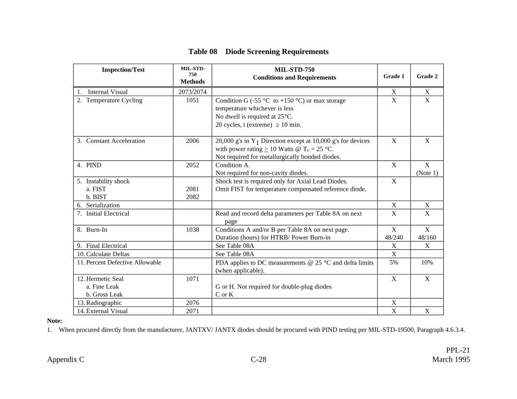
PPL-21Appendix C C-28 March 1995
Table 08 Diode Screening Requirements
Inspection/Test MIL-STD-750
Methods
MIL-STD-750Conditions and Requirements Grade 1 Grade 2
1. Internal Visual 2073/2074 X X2. Temperature Cycling 1051 Condition G (-55 °C to +150 °C) or max storage
temperature whichever is lessNo dwell is required at 25°C.20 cycles, t (extreme) ≥ 10 min.
X X
3. Constant Acceleration 2006 20,000 g's in Y1 Direction except at 10,000 g's for deviceswith power rating > 10 Watts @ TC = 25 °C.Not required for metallurgically bonded diodes.
X X
4. PIND 2052 Condition A.Not required for non-cavity diodes.
X X(Note 1)
5. Instability shocka. FISTb. BIST
20812082
Shock test is required only for Axial Lead Diodes.Omit FIST for temperature compensated reference diode.
X
6. Serialization X X7. Initial Electrical Read and record delta parameters per Table 8A on next
pageX X
8. Burn-In 1038 Conditions A and/or B per Table 8A on next page.Duration (hours) for HTRB/ Power Burn-in
X48/240
X48/160
9. Final Electrical See Table 08A X X10. Calculate Deltas See Table 08A X11. Percent Defective Allowable PDA applies to DC measurements @ 25 °C and delta limits
(when applicable).5% 10%
12. Hermetic Seala. Fine Leakb. Gross Leak
1071G or H. Not required for double-plug diodesC or K
X X
13. Radiographic 2076 X14. External Visual 2071 X X
Note:1. When procured directly from the manufacturer, JANTXV/ JANTX diodes should be procured with PIND testing per MIL-STD-19500, Paragraph 4.6.3.4.

PPL-21Appendix C C-29 March 1995
Table 08A Burn-In And Electrical Measurement Requirements For Diodes
Required Burn-In Electrical
Diode Types HTRB(Condition A)
Power(Condition B)
DeltaParameters
Measurements(Notes 1, 2, and 3)
Rectifier(Power, Fast Recovery,High Voltage)
80% rated VRM
(Note 4)125°C<TA<150°C
60 Hz SinewaveRated VRWM and IO
TA = 25 °C
∆VF
∆IR
VF, IR, VR, VBR, IFSM
trr, Cj.
Switching(General purpose,Schottky, RF, PIN)
80% rated VRM
125°C<TA<150°C60 Hz Sinewave
Rated VRWM and IO
TA = 25 °C
∆VF
∆IR
VF, VR, VBR, IR,trr, τ, Cj, Po/Pi
Zener(Voltage Reference)
Not Applicable Specify IZ to meet rated Pd
TA = 125 °C∆VZ VF, Vz, Iz
,ZZ, αVz
Current RegulatorDiode
Not required Rated VPOV
TA = 25 °C∆Is VL, ZS, ZK, Vs, Is, αIs.
Transient SuppressorDiode
80% rated VRWM
125°C<TA<150°CSpecify Ip, Tp, number of pulses
TA = 25 °C (Note 5)∆VBR
∆IR
VBR, VCM, ISM, IR.
Light Emitting Diode Not Applicable Rated IF
TA = 25 °C∆VF
∆IV
IV, IR, VF
CT
Tunnel diode(Microwave)
Rated VR
125°C<TA<150°CSpecify IF & VF to meet max. Pd
TA = 25 °C∆VP
∆VR
IP, IV, VR, VF, VV
CT
Varactor(Tuning)
80% rated VRM
125°C<TA<150°CNot Required ∆IR
∆CT
IR, VBR
CC, CT, Q, Ct1, LS, Ctz
Thyristor(SCRs)
80% rated VRM
80% rated VDM
125°C<TA<150°C
Rated VDWM & VRWM.
Specify VGT & VGQ. (Note 6)TA = 25 °C
∆IDM
∆IRM
IDM, IGM, IGT, IL, IRM, VBR, VGT,dV/dt, ton, toff
Notes:1. See MIL-S-19500, Appendix B for symbol definitions.2. Minimum required parameters are specified. When necessary, application critical parameters not listed in the table shall also be measured.3. All DC parameters shall be tested at 25°C, at minimum and at maximum operating temperatures. All AC parametric measurements shall be performed at
the required 25°C.4. Case mounted rectifiers with IO rated > 10 A @Tc= 100°C do not require HTRB.5. Refer to slash sheets (e.g. /516) for the unique power burn-in sequence of transient suppressor diodes.6. Power burn-in is applied only to SCR specifically designed with gate turn-off control; otherwise, use method 1040, condition A or B.

PPL-21Appendix C C-30 March 1995
Table 09 Transistor Screening Requirements
Inspection/Test MIL-STD-750Methods
MIL-STD-750Conditions and Requirements Grade 1 Grade 2
1. Internal Visual 207220702069
General - purpose transistorsRF transistorsPower FETs
X X
2. Temperature Cycling 1051 Condition G (-55 °C to +150 °C) or max storage temperaturewhichever is less.No dwell is required at 25°C.20 cycles, t (extreme) ≥ 10 minutes.
X X
4. Constant Acceleration 2006 20,000 g's in Y1 Direction except at 10,000 g's for devices withpower rating > 10 Watts @ Tc= 25 °C.Not required for metallurgically bonded diodes.
X X
5. PIND 2052 Condition A.Not required for optical coupled isolators.
X X(Note 1)
8. Serialization X X9. Initial Electrical Read and record delta parameters per Table 09A on next page X X10. Burn-In 1039 Conditions A and B per Table 09A on next page.
Duration (hours) for HTRB/ Power Burn-inX
48/240X
48/16011. Final Electrical See Table 09A X X12. Calculate Delta See Table 09A X X13. Percent Defective Allowable PDA applies to the DC measurements @ 25 °C and delta limits
(when applicable).5% 10%
14. Hermetic Seala. Fine Leakb. Gross Leak
1071G or HC or K
X X
15. Radiographic 2076 X16. External Visual 2071 X X
Note:1. When procured directly from the manufacturer, JANTXV/JANTX transistors should be procured with PIND testing per MIL-STD-19500, Paragraph
4.6.3.4.

PPL-21Appendix C C-31 March 1995
Table 09A Burn-In and Electrical Measurement Requirements for Transistors
Required Burn-in DeltaParameters
Electrical Measurements(Notes 1,2, and 3)
Transistor Type HTRB(Condition A)
Power(Condition B)
Bipolar Transistors(Switching, Low/ HighPower, Dual, GeneralPurpose. )
80% rated VCBO
125°C<TA<150°C
Specify VCB or VCE to meet max PT
TA = 25 °C∆ICBO or ∆ICEO
∆hFE
ICB, ICEO, ICBO, IEBO,V(BR)CEO, V(BR)CBO, V(BR)EBO,V(BR)CES, VCE(SAT), V BE(SAT),
hFE, ton, toff, ts, tf, hfe, Cobo, Cibo
Bipolar Transistors(RF, High-Frequency)
80% rated VCBO
125°C<TA<150°CSpecify VCB to meet max PT
TA = 25 °C∆ICEO
∆hFE
ICEO, V(BR)CEO, V(BR)CBO, V(BR)EBO
VCE(SAT), hFE
GPE, NF, hfe, η, Cobo
Junction Field Effect(JFET)
80% rated VGS
VDS = 0125°C<TA<150°C
80% rated VGS
Specify VDS to meet max PT
TA = 25 °C
∆IDSS or ∆IGSS
∆yfs
VDS(ON), VGS(OFF), V(BR)GSS, IGSS,IDSS, Ciss, Crss, yfs, yos.
MOSFET 80% rated VDS
VGS= 0VTA= 125 °C
80% of rated VGS
VDS= 0VTA= 125 °C
∆IDSS or ∆IGSS
∆VGS(TH)
∆rds (on)
V(BR)DSS, VGS(TH), VDS(ON), VSD,rds(on),
ton, toff, trr, CT.
Darlington 80% rated VCBO
125°C<TA<150°CSpecify VCB or VCE to meet max PT
TA = 25 °C∆hFE
∆ICE
VCE(SAT), VBE(SAT), VBE(TH),V(BR)CEO, ICEO, IEBO, ICE
hFE, ton, toff, Cobo.Optocoupler IF = 0
80% Rated VCBO
TA = 125 °C
IF = rated maxSpecify VCE to meet max PT
TA = 25 °C
∆hFE
∆IC(OFF)
∆IC(ON)
VCE(SAT), V(BR)CEO, VF
IC(OFF), IC(ON), IR,hFE, tr, tf, Cobo.
Notes:1. See MIL-S-19500, Appendix B for symbol definitions.2. Recommended electrical parameters are specified. Since electrical parameters are device dependent, the conditions and limits pertaining to a device type
shall be specified in a detail specification.3. All DC parameters shall be tested at 25°C, at minimum operating temperature and at maximum operating temperature. All AC parametric measurements
shall be made at the required 25°C.

Notice 1PPL-21
Appendix C C-32 May 1996
Table 10 Monolithic Integrated Circuit Screening Requirements
Inspection/ Test MethodsMIL-STD-883
Conditions and Requirements Grade 1 Grade 2
1. Wafer Acceptance 5007 X2. Nondestructive Bond Pull 2023 X3. Internal Visual 2010 Condition A or B (Note 1). X X4. Temperature Cycling 1010 Condition C (-65 °C to + 150 °C) in N2 atmosphere.
20 cycles.X X
5. Constant Acceleration 2001 Condition E (Note 2).Y1 orientation only.
X X
6. PIND 2020 Condition A. X X7. Radiographic 2012 1 view for Quad Flat Pack and Leadless Chip Carrier.
2 views for other package styles.Can be performed at any time after PIND.
X
8. Serialization X9. Initial Electrical Measurements Read and record delta parameters per Table 10A. X X
10. Burn-In(Note 3)
1015 Condition C and/or D per Table 10A.Duration (hours) for Static/Dynamic burn-in asrequired in Table 10A.
X72/240
X160
11. Final Electrical Measurements Per Table 10A. X X12. Calculate Deltas See Table 10A. X13. Percent Defective Allowable PDA applies to delta, selected DC and functional tests
at test temperature of 25 °C.∆+DC ≤5%
Functional ≤ 3%DC ≤10%
14. Hermetic Seala. Fine Leakb. Gross Leak
1014Condition A or B.Condition C.
X X
15. External Visual 2009 3 X to 10X. X XNotes:1. Destructive Physical Analysis may be performed to the requirements of S311-M-70 in lieu of internal visual for devices used in Grades 2 applications.2. For packages having a cavity perimeter of 2 inches or more in total length, or having a mass greater than 5 grams, test condition D can be used.3. A dynamic burn-in or a static burn-in shall be performed in accordance with Table 10A. Static and dynamic burn-in is required for Grade 1 parts when so
indicated in Table 10A. A dynamic or static burn-in shall be performed in accordance with Table 10A for Grade 2 parts.

Notice 1PPL-21
Appendix C C-33 May 1996
Table 10A Burn-In and Electrical Measurement Requirements for Monolithic ICs (Page 1 of 4)
Required Burn-In (Note 4) ElectricalIC Type Static
(Condition C)Dynamic
(Condition D)Delta Measurements
(Notes 1, 2, 3)Digital Bipolar &Digital MOS/BiCMOS: (Note 6)LOGIC (Gates, Buffers,Flip-Flops,Multiplexers, Registersand Counters)RAMsFIFOsMicroprocessorsInterface PeripheralsASICsFPGA, PROM, PLA(Note 5)
Not required for Digital BipolarTechnology.
Required for Digital MOSTechnology.
TA ≥ 125 °C
Vin= VDD across one-half input pinsand VSS across the remaininginputs.
Vout= 0.5 VDD through RL
Required for both technologies.
TA ≥ 125 °C
Vin = Square wave, 50% Duty Cycle toinput pins and control pins.
Frequency= 100 Hz to 1 Mhz.
Vout = VCC /2 or VDD/2 through RL..
∆ICC
or∆IDD
DC: VIC, VOH, VOL, ICC(IEE), IIL,IIH, IDD, IOZL, IOZH, IOS
AC: TPLH, TPHL, TTLH, TTHL, TPZH,TPHZ, TPLZ, TPZL, TA, TS, TH
Functional Tests:a) for simple logic devices,verifytruth table
b) for complex logic devices suchas ASIC, FPGA, microprocessors,functional testing includes faultcoverage calculations required perMil-Std-883, Method 5012.
c) for PROMs, check fuse map;for RAMs, perform patternsensitive tests such as March,galpat, etc.
Linear MOS, Bipolar,and Bi-FET: (Note 7)Op-Amp, InstrumentAmplifiers, S/H, andComparator
TA ≥ 125 °CVout= Terminated to ground
through RL
TA ≥ 125 °CVin= Square wave or sinewaveF= 10Hz to 100 KHz, 50% duty cycleVout= Terminated to ground through RL
∆IIB
∆IIO
∆VIO
DC: ICC, IEE, IIO, VIO, VOPP, AV,CMRR, PSRR
AC: Slew rate
See notes on page C-35.

Notice 1PPL-21
Appendix C C-34 May 1996
Table 10A Burn-In and Electrical Measurement Requirements for Monolithic ICs (Page 2 of 4)
Required Burn-In (Note 4) ElectricalIC Type Static
(Condition C)Dynamic
(Condition D)Delta Measurement
(Notes 1, 2, 3)Linear MOS, Bipolarand JFET: (Note 7)Line Drivers andReceivers
TA ≥ 125 °CVin= VDD max across one-half input
pins and VSS across theremaining inputs.
TA ≥ 125 °CVin= Square wave at a specified Vdc
Vout= VCC through RL
∆ICC
∆IIH
DC: VOH, VOL, ICC, IIL, IIH,IOS
AC: TPLH, TPHL, TTLH, TTHL
Functional Test: verifytruth table
Linear MOS, Bi-FET,and Bipolar: (Note 6)Analog Switches andMultiplexers
TA ≥ 125 °CVin= VDD max across one-half of
inputs and VSS across theother remaining inputs.
Vout= ± VCC through RL
TA ≥ 125 °CVin= Square waveF= 100 Khz and 50% duty cycleVout= ± VCC through RL
ICC
ID(OFF)
IS(OFF)
R(ON)
DC: ICC, ID(ON), R(ON),ID(OFF), IS(ON), IS(OFF)
AC: T(ON) , T(OFF)
break- before- make- timeLinear Bipolar:Voltage Regulators
TA ≥ 125 °CVout= Terminated to groundthrough RL
Not required ∆ISCD
∆VOUT
DC: ICC, VOUT, IOS,line/load regulation
Linear Bipolar:Pulse-width-modulator
Not required TA ≥ 125 °CVout= Terminated to ground through
RL
Rext, Cext connected if applicable.
∆IIO
∆VREF
DC: VREF, IIB, IIO, IOS, VIO,VOL, VOH, AV, CMRR,PSRR
AC: TR , TF, fOSC
Darlington TransistorArray
TA ≥ 125 °CVout= 15 Vdc through RL
Not required ∆ICEX
∆hFE
DC: V CE(SAT) , VF, ICEX, IF
AC: hFE, tPHL, tPLH
Linear CMOSTimers
TA ≥ 125 °C
Vout= VCC through RL
Not required ∆ICEX
∆VOH
∆VOL
DC: VTRIG, VTH, VR, VOL,VOH, VSAT, ICC, ITRIG, ITH, IR,ICEX
AC: TTLH, TTHL
See notes on page C-35.

Notice 1PPL-21
Appendix C C-35 May 1996
Table 10A Burn-In and Electrical Measurement Requirements for Monolithic ICs (Page 3 of 4)
Required Burn-In (Note 4) ElectricalIC Type Static
(Condition C)Dynamic
(Condition D)Delta Measurement
(Notes 1, 2, 3)Linear MOS andBipolar:Active Filters
Not required TA ≥ 125 °CVin= Sine wave at Frequency < fO
Vout= Terminated to ground through RL
∆ICC
∆VOS
DC: ICC, ISS, VOS
AC: fO, Q, input frequencyrange
Mixed Signal MOS,Bi-CMOS andBipolar: (Note 7)Analog to Digital(A/D) Converters.
TA ≥ 125 °CVin = Max analog dc inputVout = VCC/2 through RL
TA ≥ 125 °CVin= Analog input to generate maximum
digital codes.Vout = VCC/2 through RL
∆ICC
∆IEE
∆VIO
DC: VREF, VOH, VOL, VIO, ICC,IEE, IIL, IIH, IOZL, IOZH, IOS, ZeroError, Gain Error, LinearityError.AC: TC, TS, TH
Functional Test: Verify codesMixed Signal MOS,Bi-CMOS and Bipolar(Note 7)Digital to Analog(D/A) Converters.
TA ≥ 125 °CVin= VDD on one-half data inputs
and VSS on remaining inputs.Vout= Terminated to ground thru RL
TA ≥ 125 °CVin = Apply appropriate digital codes for
all inputs and for control signals.Vout = Terminated to ground through RL.
∆ICC
∆IEE
DC: ICC, IEE, IIL, IIH, IOZL, IOZH,IOS, Zero Error, Gain Error,Linearity Error, PSRRAC: TC, TS, TH
Functional Test: Verify codesNotes:1. See MIL-S-1331 for symbol definitions.2. These are typically recommended electrical parameters. Since electrical parameters are device dependent, refer to detail specifications for actual DC and
AC parametric test conditions and limits.3. For digital devices, all DC parameters, functional tests, and switching tests shall be tested at 25°C, at minimum operating temperature and at maximum
operating temperature. AC tests (e.g CIN) are tested initially and after any design or process changes.For linear devices, all DC parameters shall be tested at 25°C, at minimum operating temperature and at maximum operating temperature. All AC andswitching tests shall be performed at 25°C.
4. Static and Dynamic burn-in shall be performed at maximum recommended operating supply voltage with V in and RL selected to assure that the junctiontemparature shall not exceed Tjmax specified for the device type.
5. For one-time programmable devices, (e.g. PROMs, PALs and FPGAs) dynamic burn-in shall be performed on programmed devices with user applicationspecific burn-in circuit. The post burn-in should include DC, AC, and functional tests for user's program verification.
6. Dynamic burn-in required for Grade 2 parts.7. Static or dynamic burn-in acceptable for Grade 2 parts.
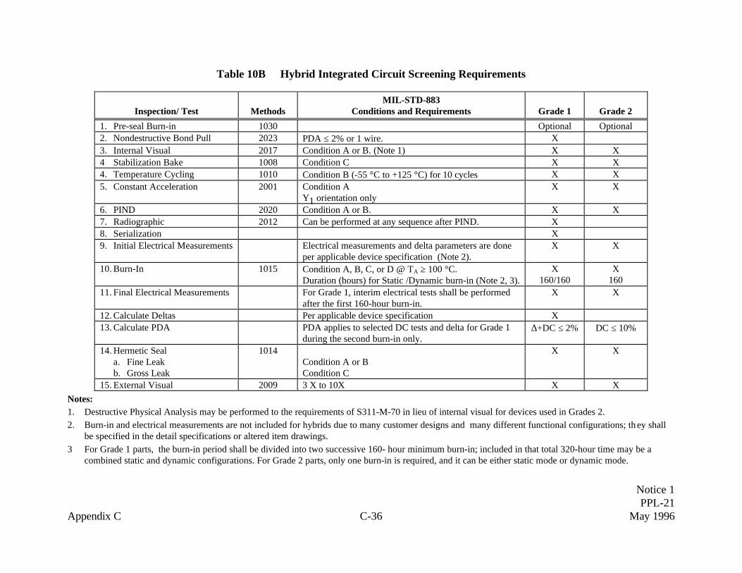
Notice 1PPL-21
Appendix C C-36 May 1996
Table 10B Hybrid Integrated Circuit Screening Requirements
Inspection/ Test MethodsMIL-STD-883
Conditions and Requirements Grade 1 Grade 2
1. Pre-seal Burn-in 1030 Optional Optional2. Nondestructive Bond Pull 2023 PDA ≤ 2% or 1 wire. X3. Internal Visual 2017 Condition A or B. (Note 1) X X4 Stabilization Bake 1008 Condition C X X4. Temperature Cycling 1010 Condition B (-55 °C to +125 °C) for 10 cycles X X5. Constant Acceleration 2001 Condition A
Y1 orientation onlyX X
6. PIND 2020 Condition A or B. X X7. Radiographic 2012 Can be performed at any sequence after PIND. X8. Serialization X9. Initial Electrical Measurements Electrical measurements and delta parameters are done
per applicable device specification (Note 2).X X
10. Burn-In 1015 Condition A, B, C, or D @ TA ≥ 100 °C.Duration (hours) for Static /Dynamic burn-in (Note 2, 3).
X160/160
X160
11. Final Electrical Measurements For Grade 1, interim electrical tests shall be performedafter the first 160-hour burn-in.
X X
12. Calculate Deltas Per applicable device specification X13. Calculate PDA PDA applies to selected DC tests and delta for Grade 1
during the second burn-in only.∆+DC ≤ 2% DC ≤ 10%
14. Hermetic Seala. Fine Leakb. Gross Leak
1014Condition A or BCondition C
X X
15. External Visual 2009 3 X to 10X X XNotes:1. Destructive Physical Analysis may be performed to the requirements of S311-M-70 in lieu of internal visual for devices used in Grades 2.2. Burn-in and electrical measurements are not included for hybrids due to many customer designs and many different functional configurations; they shall
be specified in the detail specifications or altered item drawings.3 For Grade 1 parts, the burn-in period shall be divided into two successive 160- hour minimum burn-in; included in that total 320-hour time may be a
combined static and dynamic configurations. For Grade 2 parts, only one burn-in is required, and it can be either static mode or dynamic mode.

PPL-21Appendix C C-37 March 1995
Table 14 Thermistor Screening Requirements (Page 1 of 3)
Part Type/Grade Level
Inspection/Test Test Methods, Conditions and Requirements (Note 1) Notes Positive TemperatureCoefficient
Negative TemperatureCoefficient
1 2 1 2
Visual Inspections Materials, design, construction, marking, and workmanship X X X XMechanical Inspections Body and lead dimensions to specification 2 X X X XZero-Power Resistance MIL-STD-202, Method 203
Zero-power resistance at specified reference temperatureZero-power resistance at +125°CZero-power resistance at specified reference temperature∆R (zero-power) to specification
3, 4, 5 X X X X
Thermal Shock MIL-STD-202, Method 107Grade 1 - 25 cyclesGrade 2 - 10 cyclesHigh temperature - +125°CLow temperature - min. rated operating
4, 5, 6 X X X X
High Temperature Storage +125°C, 100 hours, no load 4, 5, 6 X X X X
Zero Power Resistance MIL-STD-202, Method 203Zero-power resistance at specified reference temperature∆R (zero-power) to specification
3, 4, 5 X X X X
Insulation Resistance MIL-STD-202, Method 302Between leads and conductive material surrounding bodySpecified minimum resistance
X X X X
See notes on page C-38.

PPL-21Appendix C C-38 March 1995
Table 14 Thermistor Screening Requirements (Page 2 of 3)
Part Type/Grade Level
Inspection/Test Test Methods, Conditions and Requirements (Note 1) Notes Positive TemperatureCoefficient
Negative TemperatureCoefficient
1 2 1 2
Resistance TemperatureCharacteristic
Specified temperature pointsStabilization time ≥ 10 times the thermal time constantZero-power resistance at each temperature pointResistance curve to specification within tolerance limits at
each temperature pointTemperature points:Grade 1- reference temperature, each temperature extreme,and a minimum of 5 points between reference temperatureand each temperature extremeGrade 2- reference temperature, each temperature extreme,and a minimum of 3 points between reference temperatureand each temperature extreme
3, 4, 5 X X X X
Percent DefectiveAllowable (PDA)
Grade 1- 5%Grade 2 -10% 7 X X X X
Notes:1. It is the responsibility of the user to define minimum and/or maximum values for each parameter (pass/fail criteria). These values should be based on the
nearest equivalent military specification, manufacturer specification, or the application, whichever is most stringent.2. A minimum of three thermistors shall be measured.3. Zero-power resistance shall be measured in a controlled uniform medium capable of maintaining an accuracy of ±0.05°C for beads (any mounting
construction) and ±0.05°C for all other types. The resistance shall be measured using a wheatstone bridge (or equivalent), accuracy to ±0.05% or better,with time response less than the thermal time constant of the thermistor under test.
4. The specified reference temperature is usually ambient +25°C. However, since the resistance curve tolerance varies on either side of this referenceambient, for particular applications, it may be advantageous to specify the reference temperature at some other point, up to and including the temperatureextremes. If a temperature extreme is used as the reference temperature, the complementary temperature for zero-power resistance and resistance ratioshall be the midpoint temperature between the temperature extremes. If the high temperature extreme is < +125°C, this temperature shall be used forthermal shock and high temperature storage testing.

PPL-21Appendix C C-39 March 1995
Table 14 Thermistor Screening Requirements (Page 3 of 3)
Notes (Continued):5. Never expose a thermistor to an ambient temperature greater than its maximum operating temperature during testing under no load conditions. Such
exposure, even for brief periods, can permanently destabilize the thermistor if the Curie temperature is exceeded. The maximum operating temperature,which can be determined from the power rating, is the maximum body temperature at which the thermistor will continue to operate with acceptablestability of its characteristics. The temperature at which the power has been linearly derated to 0% corresponds to the maximum ambient temperatureunder no load conditions.
6. External visual examination required after testing to verify no evidence of mechanical damage.7. Marking defects shall not be counted for purposes of establishing the failure rate.

PPL-21Appendix C C-40 March 1995
Table 15 Transformer Screening Requirements (Page 1 of 2)
Inspection/Test Part Types Test Methods and Conditions Grade 1 Grade 2
Thermal Shock25 cycles10 cycles
All Continually monitor during final cycle toverify no intermittent conditions.Monitoring current shall be < 3 microamps.Open exceeding 100 microseconds shall bedetectable. (Note 1)
XX
Burn-InPower, No Load
Power, with maximum rated load
< 0.8 Watts Output
> 0.8 Watts Output
Duration at maximum rated temperature,rated input voltage, and current atminimum rated frequency.
96 hrs. 96 hrs.
Seal If applicable, Grade 4 of MIL-T-27 MIL-STD-202, Method 112, andMIL-T-27, Paragraph 4.8.7
X X
Dielectric Withstanding Voltage MIL-STD-202, Method 301 and Method105. Shall be measured at atmosphericpressure and at altitude in accordance withMIL-T-27, paragraph 4.8.8
X X
Induced Voltage Transformers with greater than 25volts RMS for any winding
2 times rated voltage in accordance withMIL-T-27, paragraph 4.8.9. Inspect forevidence of arcing, insulation breakdown,abrupt input current changes.
X X
Insulation Resistance All MIL-STD-202, Method 303 and MIL-T-27,paragraph 4.8.10
X X
See notes on page C-41.

PPL-21Appendix C C-41 March 1995
Table 15 Transformer Screening Requirements (Page 2 of 2)
Inspection/Test Part Types Test Methods and Conditions Grade 1 Grade 2
Electric characteristicsNo LoadRated LoadDC Resistance andResistive UnbalanceHarmonic DistortionFrequency ResponseInsertion LossSelf-Resonant FrequencyElectrostatic ShieldingMagnetic shieldingPolarityStorage Factor (Q)Wave ShapeTurns RatioPhase Shift
As Applicable As specified and in accordance withMIL-T-27, paragraph 4.8.11
X X
RadiographInspection
All MIL-STD-981, Appendix C X
Visual and MechanicalExamination
All MIL-T-27, Paragraph 4.8.1 X X
Notes:1. For Grade 1 parts with magnet wire small than 30 AWG, measure DC resistance before and after each cycle.

Notice 1PPL-21
Appendix C C-42 March 1995
Table 16 Wire and Cable Screening Requirements (Note 1) (Page 1 of 3)Wire or Cable Type/Grade Level
Inspection/ Test Methods Conditions and Insulated Magnet Coaxial MulticonductorTest Requirements 1 2 1 2 1 2 1 2
Visual Inspect for proper marking, insulation, andcolor. Check workmanship for insulationcracks, splits. For magnet wire only, checkfor blisters or runs. Use 3x magnificationand high intensity lighting.
X X X X X X X X
Mechanical (Note 2) Verify finished wire or cable diameter perreference specification. Verify propernumber of wire strands and AWG ofstrands in conductor(s) and shield (ifapplicable). Verify weight as necessary.Inspect for discoloration or corrosion of thestrands. Wire plating finish or coatingshall not flake off from normal flexing.
X X X X X X X X
Impulse Dielectric Test(Insulation/Jacket flawsTest) Not Applicable tocopper-clad Semi-RigidCable (Note 3)
FED-STD-228 Method 6211.1 or MIL-STD-2223 method 3002. Finished wire orcable shall be passed through a bead chainelectrode head which will give intimatemetallic contact with the wire insulationsurface or cable jacket. Voltage potentialas specified in detail specification shall beapplied between the electrode and wireconductor or cable shield. Wire lengthswith failed insulation shall be removed.
X X X X X X
Wrap Test(Extruded Insulations)(Note 4)
MIL-W-22759, paragraph 4.6.3.3. Sampleshall be baked for 2 hours at thetemperature specified in the detailspecification. After cooling, the sampleshall be examined for cracked insulation.
X X
Lamination Sealing Test(Tape SinteredInsulations)
MIL-W-81381, paragraph 4.7.4.10.Sample shall be baked at the temperaturespecified in the detail specification for 48hours. After cooling, visually examine fordelamination of the insulation.
X X
See notes on page C-44.

Notice 1PPL-21
Appendix C C-43 March 1995
Table 16 Wire and Cable Screening Requirements (Note 1) (Page 2 of 3)
Wire or Cable Type/Grade LevelInspection/ Test Methods Conditions and Insulated Magnet Coaxial Multiconductor
Test Requirements 1 2 1 2 1 2 1 2DC Resistance FED-STD-228, Method 6021.
Measurements shall conform to MIL-W-22759, Table II. Wire shall be tested drywithout immersion.
X X
Adherence and Flexibility(Note 5)
a. Clamp 10 inches apart, elongate asspecified and examine for insulationseparation from the wire as specified.(Note 6)
b. Wind around mandrel and examinefor cracks or separation as specified.(Note 6)
X X
Heat Shock (Note 5) Bake at maximum rated temperature for 30minutes. Examine for cracks at specifiedmagnification. (Note 6)
X X
Dielectric WithstandingVoltage (Note 7)
FED-STD-228, Method 6111, except cableshall be tested dry without immersion. Forcoaxial cable, apply voltage (potential asspecified) between inner conductor andshield with the shield grounded. Formulticonductor cable, each conductor shallbe tested against all others tied to theshield.
X(Note 8)
X(Note 8)
X X X X
Continuity(Note 7)
Apply 25 V DC max to both ends ofconductor(s), followed by both ends ofshield through an indicator (meter, light, orbuzzer).
X X X X
See notes on page C-44.

Notice 1PPL-21
Appendix C C-44 March 1995
Table 16 Wire and Cable Screening Requirements (Page 3 of 3)
Notes:1. Visual and mechanical inspection, wrap test, lamination sealing test, adherence and flexibility, and heat shock shall be performed on a 1 foot sample per
spool. Impulse dielectric test shall be performed on entire length of wire or cable. DC resistance, dielectric withstanding voltage and continuity test shallbe performed on each spool. For commercial multiconductor cable, individual wires shall have been tested in accordance with insulated wire requirementsspecified herein prior to application of shield or jacket.
2. A certificate of compliance from the manufacturer shall be required to certify that the proper conductor material and finish were used in the manufacture ofthe wire.
3. Test is used as a 100% screening test of finished wire during final winding of the wire on spools or reels by the manufacturer. Military QPL wire andcable already meet this requirement. For non-QPL wire, a certificate of compliance from the manufacturer, stating that all wire delivered to the userpassed the impulse dielectric test, is sufficient to meet this requirement. Otherwise, wire shall be screened by the user. The MIL-STD-2223 highfrequency spark test (Method 3008) is an acceptable alternative to the impulse dielectric test.
4. Test is used to determine if wire insulation is over sintered resulting in degraded properties. For Teflon insulated wire, Differential Scanning Calorimetry(DSC) per ASTM-E794 may also be performed to determine if wire is undersintered from incomplete processing. Either condition can lead to crackedinsulation during use.
5. Required for non-military, non-NEMA magnet wire only. A certificate of compliance shall be required for military, NEMA wire. Heat shock test mustfollow adherence and flexibility test.
6. Examination and Elongation Requirements for Copper Magnet Wire
AWG Size Elongation Rate MinimumElongation
Mandrel Diameter Examined With
4-9 12 ± 1 in/min (300 ± 25 mm/min) 30% none 3X - 10X magnification10-13 12 ± 1 in/min (300 ± 25 mm/min) 25% 5X 6X - 20X magnification14-30 12 ± 1 in/min (300 ± 25 mm/min) 20% 3X 10X - 30X magnification31-44 12 ± 1 in/min (300 ± 25 mm/min) 20% or breakage 3X or 0.0156 (1/64 inch drill
bit), whichever is greater30X - 70X magnification
7. Test is used as a 100% screening test of finished cable on spools or reels by the manufacturer. MIL-C-17 QPL coaxial cable and MIL-C-27500multiconductor cable already meet this requirement. For non-QPL cable, a certificate of compliance from the manufacturer, stating that all cable deliveredto the user passed the dielectric withstanding voltage and continuity tests, is sufficient to meet requirements. Otherwise, cable shall be screened by theuser.
8. For non-military, non-NEMA specified magnet wire the Dielectric Strength test of NEMA specification, MW 1000, Part 3, paragraph 3.8, or the DielectricBreakdown Voltage test of ASTM Standard D1676, paragraphs 69 and 74, shall be performed.
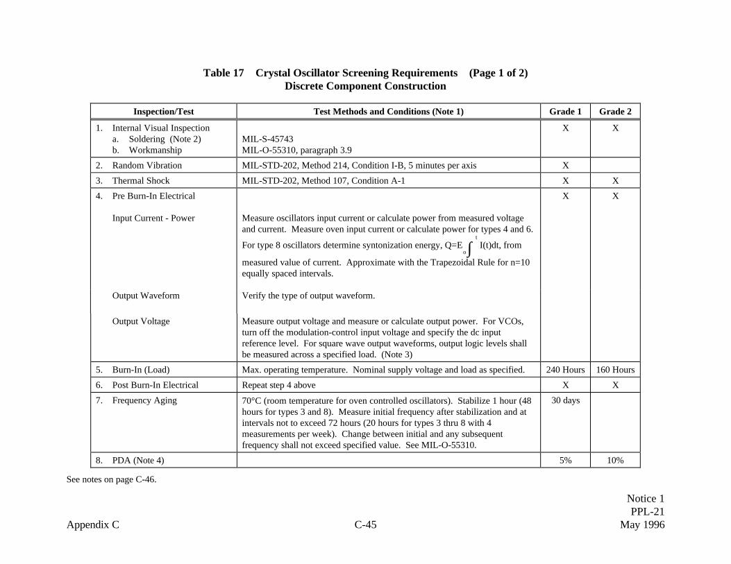
Notice 1PPL-21
Appendix C C-45 May 1996
Table 17 Crystal Oscillator Screening Requirements (Page 1 of 2)Discrete Component Construction
Inspection/Test Test Methods and Conditions (Note 1) Grade 1 Grade 2
1. Internal Visual Inspectiona. Soldering (Note 2)b. Workmanship
MIL-S-45743MIL-O-55310, paragraph 3.9
X X
2. Random Vibration MIL-STD-202, Method 214, Condition I-B, 5 minutes per axis X
3. Thermal Shock MIL-STD-202, Method 107, Condition A-1 X X
4. Pre Burn-In Electrical
Input Current - Power Measure oscillators input current or calculate power from measured voltageand current. Measure oven input current or calculate power for types 4 and 6.
For type 8 oscillators determine syntonization energy, Q=Eo∫
t I(t)dt, from
measured value of current. Approximate with the Trapezoidal Rule for n=10equally spaced intervals.
X X
Output Waveform Verify the type of output waveform.
Output Voltage Measure output voltage and measure or calculate output power. For VCOs,turn off the modulation-control input voltage and specify the dc inputreference level. For square wave output waveforms, output logic levels shallbe measured across a specified load. (Note 3)
5. Burn-In (Load) Max. operating temperature. Nominal supply voltage and load as specified. 240 Hours 160 Hours
6. Post Burn-In Electrical Repeat step 4 above X X
7. Frequency Aging 70°C (room temperature for oven controlled oscillators). Stabilize 1 hour (48hours for types 3 and 8). Measure initial frequency after stabilization and atintervals not to exceed 72 hours (20 hours for types 3 thru 8 with 4measurements per week). Change between initial and any subsequentfrequency shall not exceed specified value. See MIL-O-55310.
30 days
8. PDA (Note 4) 5% 10%
See notes on page C-46.
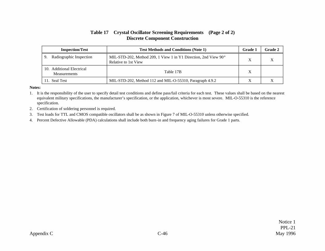
Notice 1PPL-21
Appendix C C-46 May 1996
Table 17 Crystal Oscillator Screening Requirements (Page 2 of 2)Discrete Component Construction
Inspection/Test Test Methods and Conditions (Note 1) Grade 1 Grade 2
9. Radiographic Inspection MIL-STD-202, Method 209, 1 View 1 in Y1 Direction, 2nd View 90°Relative to 1st View X X
10. Additional ElectricalMeasurements Table 17B X
11. Seal Test MIL-STD-202, Method 112 and MIL-O-55310, Paragraph 4.9.2 X X
Notes:1. It is the responsibility of the user to specify detail test conditions and define pass/fail criteria for each test. These values shall be based on the nearest
equivalent military specifications, the manufacturer’s specification, or the application, whichever is most severe. MIL-O-55310 is the referencespecification.
2. Certification of soldering personnel is required.3. Test loads for TTL and CMOS compatible oscillators shall be as shown in Figure 7 of MIL-O-55310 unless otherwise specified.4. Percent Defective Allowable (PDA) calculations shall include both burn-in and frequency aging failures for Grade 1 parts.

Notice 1PPL-21
Appendix C C-47 May 1996
Table 17A Crystal Oscillator Screening Requirements (Page 1 of 2)Hybrid Microcircuit Construction
MIL-STD-883 Test Methods and Condition (Note 1)
Inspection/Test Method Conditions Grade 1 Grade 2
1. Non Destructive Bond Pull 2023 X
2. Internal Visual 2017 C, 150°C, X X
3. Stabilization Bake (Prior toSeal)
1008 Duration (Hours) X48
X24
4. Thermal Shock 1011 A X
5. Temperature Cycling 1010 X X
6. Constant Acceleration 2001 A, Y1 only, 5000G's X X
7. PIND 2020 B X X
8. Pre Burn-In Electrical
Input Current - Power
Output Waveform
Measure oscillators input current or calculate power from measured voltageand current. Measure oven input current or calculate power for types 4 and6. For type 8 oscillators determine syntonization energy,
Q=Eo∫
t I(t)dt, from measured value of current. Approximate with the
Trapezoidal Rule for n=10 equally spaced intervals.
Verify the type of output waveform.
X X
Output Voltage Measure output voltage and measure or calculate output power. For VCOs,turn off the modulation-control input voltage and specify the dc inputreference level. For square wave output waveforms, output logic levels shallbe measure across a specified load. (Note 2)
9. 9. Burn-In (Load) 125°C, Nominal Supply Voltage and Burn-In Loads 240 Hours 160 Hours
10. Post Burn-In Electrical Repeat Step 8 Above X X
See notes on page C-48.

Notice 1PPL-21
Appendix C C-48 May 1996
Table 17A Crystal Oscillator Screening Requirements (Page 2 of 2)Hybrid Microcircuit Construction
MIL-STD-883 Test Methods and Conditions (Note 1)
Inspection/Test Method Conditions Grade 1 Grade 2
11. Frequency Aging 70°C (room temperature for oven controlled oscillators). Stabilize 1 hour(48 hours for types 3 and 8). Measure initial frequency after stabilizationand at intervals not to exceed 72 hours (20 hours for types 3 thru 8 with 4measurements per week). Change between initial and any subsequentfrequency shall not exceed specified value. See MIL-O-55310.
30 days
12. 12. PDA (Note 3) 5% 10%13. Additional Electrical
Measurements Table 17B X
14. Radiographic Inspection 2012 X X15. Seal Test
a. Fine Leakb. Gross Leak
1014A or B
C
X X
Notes:1. It is the responsibility of the user to specify detail test conditions and define pass/fail criteria for each test. These values shall be based on the nearest
equivalent military specifications, the manufacturer’s specification, or the application, whichever is most severe. MIL-O-55310 is the referencespecification.
2. Test loads for TTL and CMOS compatible oscillators shall be as shown in Figure 7 of MIL-O-55310 unless otherwise specified.3. Percent Defective Allowable (PDA) calculations shall include both burn-in and frequency aging failures for Grade 1 parts.

Notice 1PPL-21
Appendix C C-49 May 1996
Table 17B Additional Electrical Measurements (Page 1 of 2)
Test Test Methods, Conditions and Requirements (Note 1) Type (Note 2)
1. Oscillator Supply Voltage Measure voltage magnitude, tolerance, polarity, regulation, peak to peak ripple,ripple frequency and noise across oscillator input terminals with specified load.
All
2. Modulation - Control Input Voltage Same as 1 above, but also measure modulation magnitude and dc level limits or dccontrol magnitude
2, 5, 6
3. Oven Supply Voltage Same as 1 above, but measure oven voltage etc. across input terminals of oven. 4, 64. Overvoltage Survivability Apply overvoltage 20% above maximum specified supply voltage for 1 minute, with
no performance degradation. Do not exceed 16.5 volts for oscillators employingCMOS parts.
All
5. Frequency Adjustment Stabilize at reference temperature and determine by frequency measurements thatoutput signal can be set to either nominal frequency, or marked frequency offset,with specified resolution, and adjusted oven specified range.
Adjustable
6. Initial Frequency - Temperature Accuracy Stabilize at lowest specified temperature and measure frequency. Increasetemperature in specified steps (allowing stabilization), and record frequency untilhighest specified temperature is reached. Calculate frequency-temperature accuracyin accordance with paragraph 4.9.10.1.
All
7. Frequency-Voltage Tolerance Set oscillator supply voltage (oven supply voltage, if applicable) to nominal,minimum, and maximum values and measure output frequency. Determinefrequency-voltage tolerance in accordance with paragraph 4.9.14.
All
8. Rise and Fall Times Measure between specified voltage levels. For TTL and CMOS compatibleoscillators, the lower measurement level shall be 0.8 volts and 10% of signal levelrespectively. The upper measurement level shall be 2.0 volts and 90% of signallevel respectively.
Square Wave
9. Duty Cycle Measure at 50% voltage level, referenced to ground, and express as percent of waveform period. The measurement level for TTL and CMOS compatible oscillatorsshall be 1.4 volts and 50% VDD respectively.
Square Wave
10. Modulation-Control Input Impedance Apply modulation-control input voltage to input terminals through series resistance.Measure voltage across series resistor and input terminals and calculate inputimpedance in accordance with paragraph 4.9.29.
2, 5, 6
11. Frequency Deviation Assemble test equipment in accordance with Figure 13 of MIL-O-55310, andmeasure (calculate) total deviation, deviation slope polarity, and deviation linearityin accordance with paragraph 4.9.30.
2, 5, 6
See notes on page C-50.

Notice 1PPL-21
Appendix C C-50 May 1996
Table 17B Additional Electrical Measurements (Page 2 of 2)
Notes:1. It is the responsibility of the user to specify detail test conditions and define pass/fail criteria for each test. These values shall be based on the nearest
equivalent military specifications, the manufacturer’s specification, or the application, whichever is most severe. MIL-O-55310 is the referencespecification.
2. TYPESType 1 - Crystal Oscillators (XO)Type 2 - Voltage Controller Crystal Oscillators (VCXO)Type 3 - Temperature Compensated Crystal Oscillators (TCXO)Type 4 - Oven Control Crystal Oscillators (OXCO)Type 5 - Temperature Compensated-Voltage Controlled Crystal Oscillators (TCVCXO)Type 6 - Oven Controlled Voltage Controlled Crystal Oscillators (OCVCXO)Type 7 - Microcomputer Compensated Crystal Oscillators (MCXO)Type 8 - Rubidium - Crystal Oscillators (RUXO)

PPL-21Appendix C C-51 March 1995
Section 51 Recommended Screening Guidelines for Optoelectronic Parts
Table 51-01 Screening Guidelines for Detectors and Emitters
Inspection/Test MethodsMIL-STD-750
Conditions and Requirements Grade 1 Grade 2
1. Internal Visual 2073 X X(Note 1)
2. Temperature Cycling 1051 Condition G (-55 °C to +150 °C) or max storagetemperature whichever is lessNo dwell is required at 25°C.20 cycles, t (extreme) ≥ 10 min.
X X
3. Constant Acceleration 2006 20,000 g's in Y1 X X
4. PIND 2052 Condition A.Not required for non-cavity devices.
X X
5. Serialization X6. Initial Electrical and Optical
MeasurementsRead and record delta parameters per Table 51-01A onnext page
X X
7. Burn-In 1038 Per Table 51-01A.Duration (Hours)
X240
X160
8. Final Electrical See Table 51-01A X X9. Calculate Deltas See Table 51-01A X10. Percent Defective Allowable PDA applies to the combined delta calculations and DC
measurements @ 25°C.5% 10%
11. Hermetic Seala. Fine Leakb. Gross Leak
1071G or H.C or K
X X
12. Radiographic 2076 X13. External Visual 2071 X X
Note:1. DPA may be performed on 5 samples to S-311-M-70 in lieu of internal visual for sealed devices.
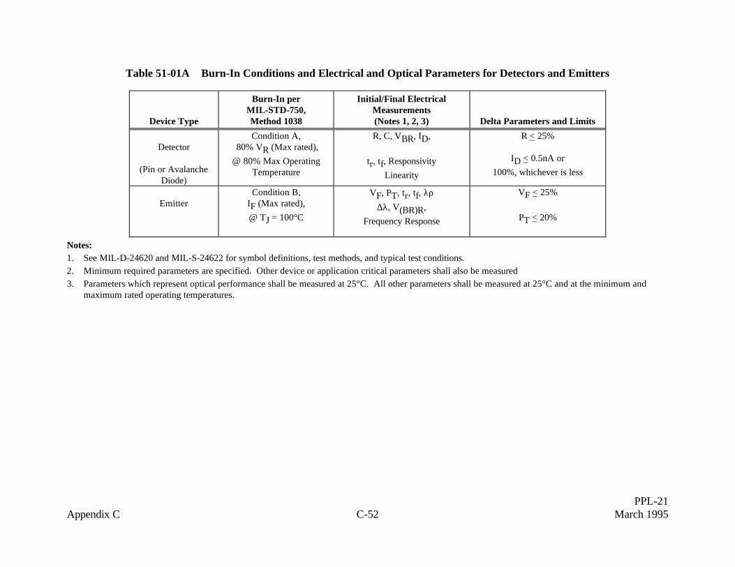
PPL-21Appendix C C-52 March 1995
Table 51-01A Burn-In Conditions and Electrical and Optical Parameters for Detectors and Emitters
Device Type
Burn-In perMIL-STD-750,Method 1038
Initial/Final ElectricalMeasurements(Notes 1, 2, 3) Delta Parameters and Limits
Detector
(Pin or AvalancheDiode)
Condition A, 80% VR (Max rated),@ 80% Max Operating
Temperature
R, C, VBR, ID,
tr, tf, ResponsivityLinearity
R < 25%
ID < 0.5nA or100%, whichever is less
EmitterCondition B,
IF (Max rated),@ TJ = 100°C
VF, PT, tr, tf, λρ∆λ, V(BR)R,
Frequency Response
VF < 25%
PT < 20%
Notes:1. See MIL-D-24620 and MIL-S-24622 for symbol definitions, test methods, and typical test conditions.2. Minimum required parameters are specified. Other device or application critical parameters shall also be measured3. Parameters which represent optical performance shall be measured at 25°C. All other parameters shall be measured at 25°C and at the minimum and
maximum rated operating temperatures.

PPL-21Appendix C C-53 March 1995
Table 51-02 Screening Guidelines for Transmitters and Receivers
The screening requirements for Hybrid Electronic Devices, given in Table 10B, are applicable for fiber optictransmitters, receivers and transceivers. In addition to the requirements for hybrid devices, these parts should be
subjected to additional connection tests if they are supplied with optical cable pigtails.
Table 51-02A Electrical and Optical Parameter Measurements for Optical Transmitters and Receivers (Note 1)
Part Type
Measurement Test Method Transmitters Receivers
Analog Digital Analog Digital
Output Short Circuit Protection MIL-STD-883, Method 3011 X X X XPower Supply Voltage andCurrent
MIL-STD-883, Method 3005 X X X X
Pulse Width Distortion and Delay(Note 1)
MIL-R-24720, Para. 4.6.4.4 X X
Jitter MIL-R-24720, Para. 4.6.4.5 XOptical Power Spectrum (Note 2) MIL-T-24721, Para. 4.6.4.2 X XOptical Power Levels (Note 2) MIL-T-24721, Para. 4.6.4.3 X XSpectral Responsivity MIL-R-24737, Para. 4.6.3.2.1 XSignal to Noise Ratio MIL-R-24737, Para. 4.6.3.3.1 X XFrequency Range MIL-R-24737, Para. 4.6.3.3.2 X XAmplitude Modulation Distoration MIL-R-24737, Para. 4.6.3.3.5 X XGroup Delay MIL-T-24735, Para. 4.6.3.3.6 X
Notes:1. For Transmitters, use MIL-T-24721, Paragraph. 4.6.4.4, 4.6.4.5 and MIL-STD-883, Method 30042. The extinction ratio measurement is not required. For Analog transmitters, a suitable analog input signal shall be used.

PPL-21Appendix C C-54 March 1995
Table 51-03 Screening Guidelines for Optical Connectors (Note 1)
Test/Inspection Test Method Conditions
MIL-STD-1344
Visual and Mechanical See Table 51-03A
Contact Engage and Separate Force(removable contacts only)
2014 Use standard mating termini orapplicable alignment sleeve.Measure axial force for compliencewith part ratings.
Hermeticity (if applicable) 1008
Notes:1. Including optical termini.
Table 51-03A Visual and Mechanical Inspections for Optical Connectors
DIMENSIONSWEIGHTKEYING
MARKING (SHELL and INSERT)WORKMANSHIP
PLATING QUALITYFERRULE QUALITY
FERRULE HOLE CIRCULARITY ANDCONCENTRICITY
INSERT QUALITY AND ORIENTATIONCONSTRUCTION AND ASSEMBLY

PPL-21Appendix C C-55 March 1995
Table 51-04 Screening Guidelines for Optical Cable
Test/Inspection Test Method Conditions
EIA/TIA-455
Visual and Mechanical See Table 51-04A
Attenuation Rate 46
Table 51-04A Visual and Mechanical Inspections for Optical Cable
QUALITY AND WORKMANSHIP OF EACH CABLECOMPONENT
EVEN DISTRIBUTION OF STRENGTH MEMBERS
DIAMETERS
MARKING
FIBER COATING ADHESION
FIBER CIRCULARITY AND CONCENTRICITY
CABLE WEIGHT

PPL-21Appendix C C-56 March 1995
THIS PAGE INTENTIONALLY LEFT BLANK

Notice 1PPL-21
Appendix D D-1 May 1996
APPENDIX D
RADIATION EFFECTS
INTRODUCTION
The space radiation environment poses a risk to all earth orbiting satellites and missions to otherplanets. Charged particles in this environment consist primarily of high energy electrons, protons,alpha particles and heavy ions (cosmic rays). The radiation effects of these charged particles aredominated by ionization (generation of electron-hole pairs) in electronic devices and materials.Energy deposited in a material by ionizing radiation is expressed in "rads", with one rad equal to100 ergs/gram (material specified). The energy loss per unit mass differs from one material toanother because of the atomic differences in various materials. For semiconductor devices, theunits of absorbed dose are rads(Si).
Radiation Effects
There are two types of radiation damage induced by charged particle ionization in the naturalspace environment. These are total dose effects and Single Event Effects (SEE). The total doseeffects are cumulative ionization damage caused by the charged particles passing through asemiconductor device. For MOS devices, this ionization traps positive charges in the gate oxideand produces interface states in silicon at the silicon-silicon dioxide interfaces. These effectscause threshold voltage shifts and decrease channel carrier mobility, resulting in increased leakagecurrent, power supply current, and possible loss of device functionality. For bipolar devices,ionization adversely affects current gain and junction leakage currents, causing significantdegradation in device performance. This performance degradation can lead to increased offsetvoltage and input bias current in op amps, and loss of accuracy and functionality in analog-to-digital converters (ADCs) or digital-to-analog converters (DACs).
Single Event Effects (SEE) are caused by a high energy single ion (heavy ion or energetic proton)passing through a device. SEE include Single Event Upsets (SEU), Single Event Latchup (SEL),Single Event Snapback, Single Event-Induced Burnout (SEB) and Single Event Gate Rupture(SEGR). While SEU are non-destructive, and do not cause permanent damage to the device, theother single event effects can be destructive under certain conditions. A brief description of theseeffects is provided below:
1. SEU or soft errors occur due to either the deposition or depletion of charge by a single ionat a circuit node, causing a change of state in the memory cell (bit upset). In very sensitivedevices, a single ion hit can also cause multiple-bit upsets (MBUs) in adjacent memorycells. However, these SEUs and MBUs cause no permanent damage and the device canbe reprogrammed for correct functioning.

Notice 1PPL-21
Appendix D D-2 May 1996
2. SEL can occur in any semiconductor device which has a parasitic n-p-n-p path. A singleheavy ion or high energy proton passing through either the base emitter junction of theparasitic n-p-n transistor, or the emitter-base junction of the p-n-p transistor can initiateregenerative action. This leads to excessive power supply current and loss of devicefunctionality. Device burnout may also occur unless the current is limited or the power tothe device is reset. SEL is of most concern in bulk CMOS devices.
3. Single Event Snapback, like SEL, is also a regenerative current mechanism, but does notrequire a n-p-n-p structure. It can be triggered in n-channel MOS transistors with largecurrents, such as IC output driver devices, by a single event hit-induced avalanchemultiplication near the drain junction of the device.
4. SEB may occur in power MOSFETs when the passage of s single heavy ion forward-biases the thin body region under the source. If the drain-to-source voltage (VDS) of thedevice exceeds the local breakdown voltage of the parasitic bipolar, the device can burnout due to large currents and high local power dissipation. If VDS is appropriately derated,it is possible to avoid SEB in power MOSFETs.
5. SEGR has been observed due to heavy ion hits in power MOSFETS when a large bias isapplied to the gate, leading to thermal breakdown and destruction of the gate oxide. Itcan also occur in nonvolatile memories such as EEPROMs during write or eraseoperations, when high voltage is applied to the gate.
A radiation risk assessment for any electronic device includes the determination of total dosedamage and SEE susceptibility of the device caused by the projected radiation environment of thespacecraft. Most total dose damage is caused by high energy protons and electrons and bysecondary radiation, such as bremsstrahlung. The major contributors to SEE are heavy ions. Thevery high fluences of high-energy protons seen during heavy solar flares and during the excursionof the satellite through the South Atlantic Anomaly (SAA) can also contribute significantly toSEE.
It should be noted that, while the total dose radiation on a device can vary significantly with theamount of shielding interposed between the device and the outside environment, the heavy ionand high-energy proton fluences (and hence the SEE susceptibility) do not change significantlywith shielding.
EVALUATION OF TOTAL DOSE SENSITIVITY OF PARTS
Total dose testing is generally performed by exposing devices to gamma rays from a Cobalt-60source (MIL-STD-883, Method 1019 for Total Dose Test Procedure). The dose rates in thenatural space radiation environment are very low (0.0001 - 0.01 rads(Si)/sec). It is not feasible tosimulate the low dose rate space environment during ground testing, because excessive timeswould be required to complete the tests. Ground test dose rates usually vary from 0.01 - 300rads(Si)/sec. For space applications, the recommended dose rates should be kept as low aspossible, preferably 0.01 - 2 rads(Si)/sec. The dose rates used depend on the predicted device

Notice 1PPL-21
Appendix D D-3 May 1996
radiation sensitivity and the projected mission total dose. Some device types and technologiesshow more variation of radiation sensitivity with dose rate than others. Most device types andtechnologies show higher total dose tolerance at low dose rates; however, some device types andtechnologies have shown increased degradation at low dose rate testing.
Available total dose test data have shown that passive devices, e.g., resistors and capacitors, showno significant degradation up to 1000 krads. Discrete semiconductor devices, such as diodes, arenot significantly affected by radiation; only small changes in reverse leakage current are observedfor total doses up to 100 krads. Most discrete bipolar transistors, e.g., 2N2222A, 2N2219 and2N2484, are not significantly affected when they are operated at high currents. However, in lowcurrent operation, gain degrades significantly after 20 to 100 krads irradiation. The radiationthreshold at which these gain degradations become significant varies with transistor type and withcollector current. However, high-power MOSFETs (such as 2N6786, 2N6788, etc.) can be verysensitive to total dose; electrical parametric degradation may occur at 2 to 5 krads and devicesmay fail catastrophically between 20 and 50 krads.
For microcircuits, the total dose tolerance varies over a wide range, from less than 1 krad to morethan 1000 krads, depending on the device's technology and manufacturing process. While bipolardigital ICs are relatively hard (resistant) to total dose effects, digital ICs with MOS or mixedBiMOS technologies can be quite susceptible to total dose. Analog devices using MOS andBiMOS technologies have shown significant degradation in the range of 2 - 20 krads.Furthermore, recent test data have shown that bipolar linear devices, such as op amps andcomparators, when tested at low dose rates (0.001 - 10 rads(Si)/sec), show significantdegradation in the range of 5-50 krads. In earlier work, when testing was done at higher doserates, bipolar linear devices were found to be radiation-tolerant to exposures ranging from 50 to100 krads.
Microcircuit radiation hardness varies not only with the device type and technology, but also withsubtle process variations within a manufacturing line over different wafer lots. Radiation testresults strongly depend on test details, such as the nature of the irradiating source, bias conditionand dose rates. All these factors make it difficult to specify a hardness level for a particulartechnology and part type. When using non-radiation-hard devices, it is recommended thatsamples from flight lots be tested for radiation tolerance.
Another device category which may be affected significantly by radiation is optoelectronicdevices, such as those used in fiber optics communication systems. These systems include opticalfibers, light sources (emitters), light detectors, connectors and couplers. A number of emitters,detectors, connectors and couplers are not adversely affected by ionizing radiation up to 100krads; however, non-radiation hardened optical fibers may exhibit attenuations several timesgreater than their intrinsic losses during low level (a few krads) total dose irradiation. Radiationinduced losses in fibers vary significantly with fiber composition and with total dose magnitudeand rate, wavelength of measurement, ambient temperature, time after exposure, length of fiberexposed and light injection conditions.

Notice 1PPL-21
Appendix D D-4 May 1996
EVALUATION OF SEE SENSITIVITY OF PARTS
Evaluation of SEE sensitivity varies with the device type. For example, for a digital device, suchas a shift register or memory, it includes evaluation of SEU and SEL sensitivity. For bipolaranalog devices, such as op amps, ADCs and DACs, the same two effects are evaluated; however,SEL is of more significant concern. For power MOSFETs, SEGR and SEB are more significantdegradation and failure mechanisms.
SEE rates for predicted space radiation environments are estimated using heavy ion and protontest data taken at an accelerator or a cyclotron facility. These data include the Linear EnergyTransfer (LET) threshold and the device error crossection. To predict upset rates, the LETspectra for each mission are determined using orbital parameters, shielding estimates and theappropriate solar activity levels. The LET spectra, LET threshold and device error cross sectionare analytically modeled to calculate the upset rate. The error rate calculations involve complexcomputations and several approximations regarding device geometry, sensitive volume anduncertainties in the heavy ion and high energy proton fluence. Two frequently used analyticalmodels for upset rate calculation are CREME (Cosmic Ray Effects on Microelectronics) andIntegral Error Rate Prediction Technique.
In order to assure system hardness, each project should perform an application analysis for all ofits electronic parts which may be susceptible to SEE. The analysis should account not only forthe number of SEE occurrences anticipated during the mission-lifetime, but also for the worst-case SEE rates resulting from transient peaks in the radiation environment, such as high protonfluences from solar flares and the SAA. This analysis is performed based on available SEE data,but may often require specific testing of parts for evaluation of their SEE sensitivity. To mitigatethe effect of SEE in sensitive parts, hardware and software techniques such as error detection andcorrection, redundancy and fault tolerance schemes, and current limiting resistors in power supplycircuits can be used.
SELECTION OF RADIATION-HARD PARTS
In recent years, a number of vendors have qualified some of their part technologies to thefollowing standard total dose radiation levels: 3 K, 10 K, 50 K, 100 K, 300 K, 600 K and 1 Mrad. Parts qualified to these levels are identified in MIL-I-38535 and MIL-S-19500 by thesymbols M, D, L, R, F, G and H respectively, substituted as a replacement symbol for the slashmark (denoting non-radiation-hardened) in the part markings. Most of these radiation-hard partsare digital part types; very few linear part types are available as rad-hard.
Parts which are hardened to various total-dose radiation levels are not necessarily less sensitive toSEE. For radiation-hardening to SEE, some manufacturers are using cross- coupled resistors inmemory cells to achieve SEU hardness for space applications. Also, some manufacturers arefabricating parts using Silicon-On-Insulator (SOI) technology, which guarantees SEL hardness.
While designing systems for space applications, use of available radiation hardened parts isrecommended. However, cost and performance requirements and schedule constraints can often
Notice 1PPL-21
Appendix D D-5 May 1996
restrict the use of available radiation-hard parts and lead the designers to use non-radiation-hardparts. The use of parts in RAD-PAK which incorporates radiation shielding in the microcircuitpackage, can enable non-radiation-hardened chips to be used in a number of space applications. Itshould be noted that, while the RAD-PAK can improve the total dose radiation tolerance of thedevices up to 100 krads, the device sensitivity to SEE is not reduced. The Parts Branch RadiationSpecialist can provide additional guidance and information concerning the selection of partssuitable for mission-radiation requirements.
In evaluating the suitability of electronic devices in their intended application, it is of extremeimportance to determine the radiation environment to which these parts will be subjected. Theradiation environment varies significantly with orbital parameters and solar activity level. Also,the radiation environment experienced by a device inside the spacecraft is affected by the shieldingprovided by the spacecraft walls and other materials interposed between the device and theoutside environment. Therefore, the radiation environment must be characterized for each projectbefore assessing the total dose and SEE sensitivity of the devices selected for system design.
RADIATION TEST DATA
The JPL RADATA Data Bank provides a significant amount of SEE and total dose testinformation. This data bank is sponsored by the NASA Office of Safety, Reliability,Maintainability and Quality Assurance (Code Q) and is carried out by the JPL Electronic PartsReliability Section 514. It is accessible via a user’s personal computer using either a modem orinternet. The procedure to access this data bank is provided below.
Procedure to Access JPL RADATA Bank
Via MODEM Via INTERNETBBS#: (818) 393-1725 FTP: radata.jpl.nasa.govFull Duplex (up to 14.4 Kbaud) (137.79.11.2)8 bits USERID: radata1 stop PASSWORD: guestno parity
For questions regarding RADATA BBS, please contact Keyvan Eslami at (818) 354-1715.
Test results from a number of radiation labs, manufacturers, etc., can also be found in"Proceedings of IEEE Annual Conference on Nuclear and Space radiation Effects", publishedfrom l977 through 1994 in the December issue of IEEE Transaction on Nuclear Science, Vols.24-41. Radiation characterization data may also be available form the part manufacturer. Thesedata should be used only as guidelines, because the radiation response of the project flight partscan vary significantly from the reported test data.

Notice 1PPL-21
Appendix D D-6 May 1996
Goddard Test Data
A significant amount of radiation testing has been performed recently on a variety of device typesbeing used in Goddard projects. Table I lists parts which were tested for total dose radiationtolerance between January 1991 and the present. Testing was performed at low dose ratesvarying from 50 - 5,000 rads(Si)/hour (0.01 - ~1.4 rads(Si)/sec), depending on the project's totaldose radiation requirements. Typical radiation test ranges were from 2.5-5 krads to 100-300krads. Typical radiation test levels were 2.5,5,7.5,10, 15, 20, 30, 50, 75, 100, 200 and 300 krads,depending upon the project’s radiation environment and the predicted radiation tolerance of theparts. Most of the parts tested were not guaranteed by the manufacturer for radiation hardness.Some parts showed significant degradation at the first radiation level, while others passedthroughout all irradiation and annealing steps. For information related to radiation-induceddegradation or failure in the test level range, Lot Date Code of the parts tested and other details,refer to the report number cited in Table I.
Table II lists the parts that have been tested for SEE for GSFC projects from 1990 to the present.These tests were performed on microcircuits and optoelectronic devices, and included both SingleEvent Upset (SEU) and Single Event Latchup (SEL) tests. Testing was performed using high-energy protons and heavy ions at the following laboratories:
i) Brookhaven National Laboratories (BNL)ii) Harvard University (HU)iii) Indiana University (IU)iv) University of California at Davis (UCD)
Qualified users may obtain a copy of Goddard radiation test data on any part type listed in Table Iand Table II by submitting a request through their project office to the Office of Flight Assurance(OFA) Information Center. Please cite the PPM report number in your request.

Notice 1PPL-21
Appendix D D-7 May 1996
Table I: Total Dose Radiation Testing for Goddard Projects (Page 1 of 8)
It should be noted that radiation results vary significantly with the Lot Date Code and anyvariation in the process technology by the manufacturer, as well as with details of the radiationtesting, such as dose rate, bias conditions, electrical parameters and functional characteristicsmeasured. The information in these reports is for general guidance only and is subject tochange at any time.
S/N Part Number Part Type Manufacturer Project Report
1 HS2-3530RH-Q Op Amp Harris ISTP/CB PPM-91-003
2 54HSC161CSO 4 bit counter Marconi ISTP/CB PPM-91-008
3 HCS4538KMSR Multivibrator Harris ISTP/CB PPM-91-004
4 MAR7001CB2 512x9 FIFO Marconi ISTP/CB PPM-91-039
5 HS5212B 12 bit ADC Sipex SMEX/CB PPM-91-048
6 IDT7203L650DB 2kx9 FIFO IDT ISTP/NC PPM-91-061
7 MR8251A/B USART Intel SMEX/CB PPM-91-053
8 HM1-6617-883 2kx8 PROM Harris ISTP/CB PPM-91-065
9 82C59A INTR Controller Harris SMEX/CB PPM-91-075
10 AD96687TQ/883B Dual Comparator Analog Devices ISTP/NC PPM-91-097
11 PM-1012AZ/883 OP AMP PMI SMEX/CB PPM-91-120
12 MC35181U OP AMP Motorola ISTP/NC PPM-91-109
13 JTXV1N759A-1 Zener Diode BKC Intnl ISTP/NC PPM-91-123
14 SI9110AK Switch Cntrl Siliconix SMEX/CB PPM-91-124
15 54AC08 2-Input NAND NSC SMEX/CB PPM-91-136
16 JTXV1N3600 Diode NSC ISTP/NC PPM-91-154
17 SQXO-2-100 KHz Crystal Osc. Statek Hydra rad-91-2
18 LP2951H/883 Adj. Volt Reg. NSC ISTP/NC PPM-91-156
19 HA1-5320-8 S/H Amp Harris ISTP/NC PPM-91-163
20 FRL130R3 N-MOSFET Harris SMEX/CB PPM-91-168
21 54ACT245 Transceiver NSC SMEX/CB PPM-91-191
22 SG1524B PWM Silicon Gen. SMEX/CB PPM-91-228
23 PALCE22V10H PLA AMD Modis-T rad-91-4
24 JTXV1N3595 Diode NSC ISTP/NC PPM-91-246
25 54AC161 Counter NSC SMEX/CB PPM-91-252
26 MC35184L Quad OP AMP Motorola ISTP/NC PPM-91-255
27 54AC138DMQB DEMUX NSC SMEX/CB PPM-91-267
28 LM160 Volt Comparator NSC ISTP/NC PPM-91-268
29 HI1-506A 16-Analog MUX Harris TIROS/BASG rad-91-6
30 JTXV2N6798 N-MOSFET GE Waves rad-91-10
31 JTXV2N6849 P-MOSFET IRC Waves rad-91-9
32 2N4117A-1 N-JFET Siliconix ISTP/NC PPM-91-335
33 NCS4538KMSR Multivibrator Harris ISTP-CB PPM-91-337

Notice 1PPL-21
Appendix D D-8 May 1996
Table I: Total Dose Radiation Testing for Goddard Projects (Page 2 of 8)
S/N Part Number Part Type Manufacturer Project Report
34 OP43AJ/883 OP AMP PMI ISTP/NC PPM-91-363
35 SQXO-2-200 KHz Crystal Osc. Statek Hydra rad-91-8
36 54AC04 Hex Inverter NSC SMEX/CB PPM-91-376
37 ADC0808MJB 8 bit ADC TI ISTP/NC PPM-91-330
38 OPA2107SM OP AMP Burr-Brown ISTP/NC PPM-91-375
39 MP5010NT Volt Reference Micro Power ISTP/NC PPM-91-383
40 MCM1609-21.86 KHz Crystal Osc. Q-Tech. Corp ISTP/NC PPM-91-382
41 CS7820-UD 8 bit ADC Crystal Semi ISTP/NC PPM-91-384
42 AD571SD 10 bit ADC Analog Devices ISTP/NC PPM-91-364
43 MC1350 OP AMP Austin Semi ISTP/NC PPM-91-391
44 LM108A OP AMP Linear Tech ISTP/NC PPM-91-392
45 DIH-149 Sol St Relay Dionics GPEP rad-91-12
46 SNJ54HC85 4 bit Compar TI ISTP/NC PPM-91-412
47 AD7224UQ/883 8 bit DAC Analog Devices ISTP/NC PPM-91-390
48 CA3127F NPN Array Harris ISTP/NC PPM-91-406
49 M54HC08YBF AND Gate SGS Thomson ISTP/NC PPM-91-407
50 CMP01 Comparator PMI ISTP/NC PPM-91-393
51 JAN2N2608 JFET XSTR Motorola ISTP/NC PPM-91-424
52 2N3946 NPN XSTR Motorola ISTP/NC PPM-91-422
53 82C59A-5 INTR Cntrllr Harris ISTP/GEO PPM-91-439
54 MT2815T/ES DC/DC Conv Interpoint SMEX/CB PPM-91-438
55 54AC245 8-Transceiver NSC SMEX/CB PPM-91-442
56 54AC00 2-Input NAND NSC SMEX/CB PPM-91-440
57 54AC86 OR Gate NSC SMEX/CB PPM-91-441
58 54AC14 Hex Inverter NSC SMEX/CB PPM-91-443
59 54AC109 JK Flip-Flop NSC SMEX/CB PPM-91-437
60 54CA11 AND Gate NSC SMEX/CB PPM-91-425
61 AD847 OP AMP Analog Devices ISTP/NC PPM-91-394
62 AD549SH/883 OP AMP Analog Devices ISTP/NC PPM-91-455
63 JTXV4N49 Opto-Coupler TI ISTP/NC PPM-91-459
64 HA1-5134 Quad OP AMP Harris ISTP/NC PPM-91-478
65 MC708-149 Crystal Osc McCoy Elec MODIS-T PPM-91-483
66 LF111H-MIL Volt Comparator NSC ISTP/NC PPM-91-481
67 CA3080A Transcon Amp Harris ISTP/NC PPM-91-484
68 54ACO2DMQB NOR Gate NSC SMEX/CB PPM-91-508
69 TSC426MJA MOSFET Driver Teledyne MODIS/T PPM-91-509
70 HA7-5170-8 OP AMP Harris ISTP/CB PPM-91-533
71 FRL913OR3 P-Power MOSFET Harris ISTP/WAVES PPM-91-534

Notice 1PPL-21
Appendix D D-9 May 1996
Table I: Total Dose Radiation Testing for Goddard Projects (Page 3 of 7)
S/N Part Number Part Type Manufacturer Project Report
72 MN91204 12 Bit DAC Micro Networks SMEX/CB PPM-91-522
73 IRHF7230 N-Power MOSFET IRC ISTP/WAVES PPM-91-587
74 2299000-1, -2 1M Bit SRAMs Teledyne GPEP/PPL PP<-91-587
75 DM28C256-300/B EEPROM SEEQ Tech. ISTP/L3 PPM-91-610
76 UDS2983 Voltage Driver Sprague Elec SMEX/CB PPM-91-551
77 54AC139DMQB 2 to 4 Decoder NSC SMEX/CB PPM-91-628
78 SMJ320C30 32-Bit DSP TI ISTP/NC PPM-91-612
79 54AC191 4 Bit Cntr NSC SMEX/CB PPM-91-614
80 SMEX 5955-03/8 Crystal Osc. Q-Tech Corp SMEX/CB PPM-91-645
81 54AC32 Quad 2-In. OR NSC SMEX/CB PPM-91-645
82 TSC43OMJA MOSFET Driver Teledyne MODIS-T PPM-91-637
83 2n5087 PNP Amp XSTR Motorola ISTP/NC PPM-91-654
84 DPAD1-3 pA Dual Diodes Interfet Corp ISTP/NC PPM-91-655
85 LF441 OP AMP NSC ISTP/NC PPM-91-656
86 ZQO4031 32k x 8 SRAM Elmo/Hitachi GPEP/PPL PPM-91-702
87 S128K8L-55MC 128k x 8 SRAM Inova GPEP/PPL PPM-91-696
88 54ACT244LMQB Octal Buffer NSC SMEX/CB PPM-91-693
89 54AC20LMQB 4-Input NAND NSC SMEX/CB PPM-91-692
90 OP232TX LED Optak Tech ISTP-711 PPM-91-703
91 2N6453 N-JFET Interfet ISTP/NC PPM-91-707
92 2298855-2 DC/DC Converter Teledyne SMEX/CB PPM-91-709
93 54AC157DMQB Quad 2-Inp MUX NSC SMEX/CB PPM-91-706
94 54ACTQ373 Octal Letch NSC GPEP PPM-91-713
95 54ACTQ08 2-Input AND NSC GPEP PPM-91-712
96 54ACTQ374 Flip-Flop NSC GPEP PPM-91-744
97 54AC74DMQB D Flip-Flop NSC SMEX/CB PPM-91-746
98 54ACT240 Octal Buffer NSC SMEX/CB PPM-91-747
99 54AC151LMQB 8 Input MUX NSC SMEX/CB PPM-91-755
100 U401-2 Dual N-JFET Siliconix ISTP/NC PPM-91-757
101 JTXV2N3868 PNP XSTR N. England Semi SMEX/CB PPM-91-759
102 54AC521DMQB 8 Bit Comp NSC SMEX/CB PPM-91-754
103 54ACT74LMQB Dual D Flip-Flop NSC SMEX/CB PPM-91-760
104 AD7541ATQ 12-Bit DAC Analog Devices GPEP PPM-91-710
105 54AC153LMQB 4-Input MUX NSC SMEX/CB PPM-91-762
106 54ACT138LMQB 1 to 8 Decoder NSC SMEX/CB PPM-92-010
107 AD574AT 12 Bit ADC Analog Devices GPEP PPM-92-011
108 HA2620 OP AMP Harris GPEP PPM-92-023
109 54ACT374LMQB Octal Flip-Flop NSC SMEX/CB PPM-92-003

Notice 1PPL-21
Appendix D D-10 May 1996
Table I: Total Dose Radiation Testing for Goddard Projects (Page 4 of 8)
S/N Part Number Part Type Manufacturer Project Report
110 AD524 Instr. Amp. Analog Devices GPEP PPM-92-029
111 54ACT157DMQB Quad 2-Inp. MUX NSC SMEX/CB PPM-92-001
112 54AC374DMQB Oct. Flip-Flop NSC SMEX/CB PPM-92-004
113 54AC04DMQB hex Inverter NSC SMEX/CB PPM-92-009
114 2N5096 PNP Transistor SSDI ISTP/EPACT PPM-92-036
115 2N5097 NPN Transistor SSDI ISTP/EPACT PPM-92-037
116 54ACT373LMQB Octal Latch NSC SMEX/CB PPM-92-044
117 54AC373DMQB Octal Latch NSC SMEX/CB PPM-92-032
118 54AC244DMQB Octal Buffer NSC SMEX/CB PPM-92-039
119 54AC646LMQB Octal Trans. NSC SMEX PPM-92-054
120 AD544SH/883B Op Amp Analog Devices ISTP/711 PPM-92-055
121 54AC20DMQB 4-Input NAND NSC SMEX PPM-92-057
122 PA07M/883 Op Amp Ampex GGS PPM-92-058
123 54AC299LMQB Shift Register NSC SMEX PPM-92-060
124 54AC540LMQB Octal Buffer NSC SMEX PPM-92-062
125 AD524 Instr. Amp Analog Devices SMEX PPM-92-069
126 CD54HC74F3 D Flip-Flop RCA GGS/WIND PPM-92-075
127 ICL766MJA/883B Dual FET Driver Harris ISTP/PA PPM-92-080
128 AD713TQ/883B Op Amp Analog Devices ISTP/PA PPM-92-079
129 AD829SQ/883B Video Op Amp Analog Devices GGS/WIND PPM-92-092
130 NC4011BM2RB 2-Input NAND SGS Thomson GGS/WIND PPM-92-101
131 M54NC373YBF Octal Latch SGS Thomson GGS/WIND PPM-92-099
132 M54HC4020YBF Binary Counter SGS Thomson GGS/WIND PPM-92-094
133 JTXV2N6788 Power MOSFET Siliconix GGS/WIND PPM-92-103
134 JM38510/11108 SPDT Switches Intersil EP/MMS/PA PPM-92-110
135 CD54HC40103F3A 8-Bit Down Ctr. RCA GGS/WIND PPM-92-115
136 CD54HC4053F3A Mux/Dmux RCA GGS/WIND PPM-92-116
137 JTXV4N49 Opto-Coupler TI CDS/CS2 PPM-92-114
138 HCC4053BM3RB Mux/Dmux SGS Thomson GGS/WIND PPM-92-122
139 AD674AT 12-Bit ADC Analog Devices POLAR-UVI PPM-92-131
140 AD565ASH 12-Bit DAC Analog Devices ISTP/HYDRA PPM-92-132
141 AG1562B PWM Silicon Gen. CDS/CS2 PPM-92-152
142 AD744TQ/883B Op Amp Analog Devices GGS/WIND PPM-92-159
143 AD711TQ/883B Op Amp Analog Devices GGS/WIND PPM-92-160
144 AD712TQ/883B Dual Op Amp Analog Devices GGS/WIND PPM-92-163
145 MP7623TD/883B D/A Conv Micro Power GGS/WIND PPM-92-170
146 AD7541ATQ/883B D/A Conv Analog Devices GGS/WIND PPM-92-171
147 SNJ54HC4075J OR-Gate TI GGS/WIND PPM-92-177
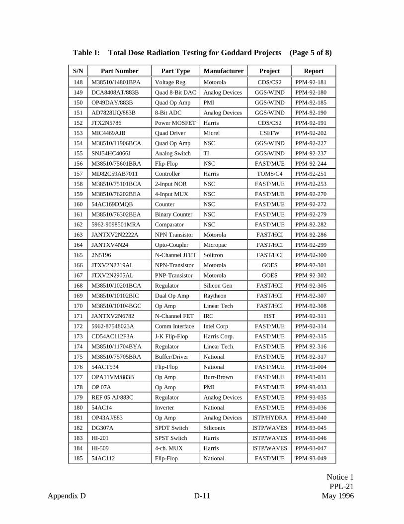
Notice 1PPL-21
Appendix D D-11 May 1996
Table I: Total Dose Radiation Testing for Goddard Projects (Page 5 of 8)
S/N Part Number Part Type Manufacturer Project Report
148 M38510/14801BPA Voltage Reg. Motorola CDS/CS2 PPM-92-181
149 DCA8408AT/883B Quad 8-Bit DAC Analog Devices GGS/WIND PPM-92-180
150 OP49DAY/883B Quad Op Amp PMI GGS/WIND PPM-92-185
151 AD7828UQ/883B 8-Bit ADC Analog Devices GGS/WIND PPM-92-190
152 JTX2N5786 Power MOSFET Harris CDS/CS2 PPM-92-191
153 MIC4469AJB Quad Driver Micrel CSEFW PPM-92-202
154 M38510/11906BCA Quad Op Amp NSC GGS/WIND PPM-92-227
155 SNJ54HC4066J Analog Switch TI GGS/WIND PPM-92-237
156 M38510/75601BRA Flip-Flop NSC FAST/MUE PPM-92-244
157 MD82C59AB7011 Controller Harris TOMS/C4 PPM-92-251
158 M38510/75101BCA 2-Input NOR NSC FAST/MUE PPM-92-253
159 M38510/76202BEA 4-Input MUX NSC FAST/MUE PPM-92-270
160 54AC169DMQB Counter NSC FAST/MUE PPM-92-272
161 M38510/76302BEA Binary Counter NSC FAST/MUE PPM-92-279
162 5962-9098501MRA Comparator NSC FAST/MUE PPM-92-282
163 JANTXV2N2222A NPN Transistor Motorola FAST/HCI PPM-92-286
164 JANTXV4N24 Opto-Coupler Micropac FAST/HCI PPM-92-299
165 2N5196 N-Channel JFET Solitron FAST/HCI PPM-92-300
166 JTXV2N2219AL NPN-Transistor Motorola GOES PPM-92-301
167 JTXV2N2905AL PNP-Transistor Motorola GOES PPM-92-302
168 M38510/10201BCA Regulator Silicon Gen FAST/HCI PPM-92-305
169 M38510/10102BIC Dual Op Amp Raytheon FAST/HCI PPM-92-307
170 M38510/10104BGC Op Amp Linear Tech FAST/HCI PPM-92-308
171 JANTXV2N6782 N-Channel FET IRC HST PPM-92-311
172 5962-87548023A Comm Interface Intel Corp FAST/MUE PPM-92-314
173 CD54AC112F3A J-K Flip-Flop Harris Corp. FAST/MUE PPM-92-315
174 M38510/11704BYA Regulator Linear Tech. FAST/MUE PPM-92-316
175 M38510/75705BRA Buffer/Driver National FAST/MUE PPM-92-317
176 54ACT534 Flip-Flop National FAST/MUE PPM-93-004
177 OPA11VM/883B Op Amp Burr-Brown FAST/MUE PPM-93-031
178 OP 07A Op Amp PMI FAST/MUE PPM-93-033
179 REF 05 AJ/883C Regulator Analog Devices FAST/MUE PPM-93-035
180 54AC14 Inverter National FAST/MUE PPM-93-036
181 OP43AJ/883 Op Amp Analog Devices ISTP/HYDRA PPM-93-040
182 DG307A SPDT Switch Siliconix ISTP/WAVES PPM-93-045
183 HI-201 SPST Switch Harris ISTP/WAVES PPM-93-046
184 HI-509 4-ch. MUX Harris ISTP/WAVES PPM-93-047
185 54AC112 Flip-Flop National FAST/MUE PPM-93-049

Notice 1PPL-21
Appendix D D-12 May 1996
Table I: Total Dose Radiation Testing for Goddard Projects (Page 6 of 8)
S/N Part Number Part Type Manufacturer Project Report
186 54AC240 Buffer/Driver National FAST/MUE PPM-93-050
187 54AC193 Binary Counter Harris FAST/MUE PPM-93-051
188 CJ28C256 32Kx8EEPROM SEEQ BCMS/GCMS PPM-93-052
189 UC1845J/883 PWM Unitrode FAST/MU3 PPM-93-059
190 MQ80386-20 µP Intel SMEX/FAST PPM-93-062
191 OW628128CD 12Kx8 RAM Hitachi FAST/MU3 PPM-93-063
192 HM628128LP-10 12Kx8 RAM Harris SMEX/FAST PPM-93-065
193 HX6464 64Kx1 SRAM Honeywell GPEP/PPL PPM-93-064
194 54AC Annealing 54AC parts GPEP PPM-93-061
195 OMH3075S Hall Eff. Sensor Optek SWAS/MUE PPM-93-070
196 8002300 5-tap Delay Line Hytek HST/COP PPM-93-078
197 G311P759-4M19430 Oscillator Monitor FAST/MUE PPM-93-101
198 G311P759/01-18M Oscillator Monitor FAST/MUE PPM-93-102
199 54HC4051 MUX/DMUX Harris ISTP/SOHO PPM-93-104
200 54HC123 Multivibrator Hrris GGS/WIND PPM-93-105
201 LP2951 Regulator National ISTP/SOHO PPM-93-106
202 MP7628 D/A Converter Micro Power ISTP/SOHO PPM-93-108
203 54HC165 Shift Register Motorola ISTP/SOHO PPM-93-107
204 LM108A Op Amp National ISTP/SOHO PPM-94-001
205 54ACQT08 AND Gate National SMEX/FAST PPM-94-003
206 AD7672 A/D Converter Analog Devices ISTP/SOHO PPM-94-004
207 A1020B Gate Array Actel GPEP/PPL PPM-94-005
208 LM139 Comparator National CASSINI PPM-94-008
209 LM139 Comparator PMI GOES/SXI PPM-94-010
210 5406 Inverting Buffer TI GOES/SXI PPM-94-011
211 1280A Gate Array Actel GPEP/PPL PPM-94-012
212 LM139 Comparator National CASINI/INMS PPM-94-013
213 54HC4053 MUX/DEMUX Harris ISTP/SOHO PPM-94-014
214 PA10A Power Op Amp Apex Microtech CASSINI PPM-94-015
215 OP177A Op Amp Analog Devices FUSE PPM-94-016
216 AD7545 D/A Converter Analog Devices FUSE PPM-94-017
217 EL2243 Dual Op Amp Elantec FUSE PPM-94-018
218 LF411 Op Amp National FUSE PPM-94-019
219 OP 07A Op Amp Linear Tech. EOS/AM PPM-94-020
220 LM108A Op Amp Linear Tech. EOS/AM PPM-94-022
221 26C31 Quad Op Amp National FUSE PPM-94-023
222 ADC0816 8-bit ADC/MUX National FUSE PPM-94-025
223 54AC299 Shift Register National EOS/AM PPM-94-026

Notice 1PPL-21
Appendix D D-13 May 1996
Table I: Total Dose Radiation Testing for Goddard Projects (Page 7 of 8)
S/N Part Number Part Type Manufacturer Project Report
224 54AC374 D-type Flip-Flop National EOS/AM PPM-94-027
225 LM108 Op Amp National CASSINI PPM-94-028
226 TC4420 MOSFET Buffer Teledyne GOES/SXI PPM-94-035
227 82C54 Interval Timer Intel HST/BASE PPM-94-036
228 OP400AY Quad Op Amp Analog Devices HST/ADD PPM-94-037
229 LM139 Comparator National CASSINI PPM-94-038
230 DAC08A D/A Converter Analog Devices CASSINI PPM-95-103
231 F100324 Translator National EOS/AM PPM-94-040
232 7204 FIFO IDT HST/BASE PPM-95-101
233 F100325 Translator National EOS/AM PPM-95-102
234 LM10 Op Amp Linear Tech. HST/CAL PPM-95-105
235 RP7820 A/D Converter Space Elec., Inc. CASSINI PPM-95-107
236 AD565 D/A Converter Analog Devices CASSINI PPM-95-108
237 TL074 Quad Op Amp TI HST/CAL PPM-95-109
238 TSC4429 MOSFET Driver TI CASSINI PPM-95-110
239 HCPL-5631 Optocoupler HP HST/STIS PPM-95-113
240 LM10 Op Amp National HST/CAL PPM-95-115
241 SDM3304 NPN Transistor Solitron HST/CAL PPM-95-118
242 IDT49C460 Error Detector IDT HST/BASE PPM-95-119
243 MD82C59A Controller Harris HST/BASE PPM-95-123
244 AD677 A/D Converter Analog Devices HST/BASE PPM-95-124
245 MFL2805S DC/DC Conv. Interpoint HST/PCP PPM-95-126
246 MFL2815S DC/DC Conv. Interpoint HST/PCP PPM-95-127
247 MFL2812S DC/DC Conv. Interpoint HST/PCP PPM-95-128
248 OP27A Op Amp LTC CASSINI PPM-95-129
249 MC1717 Motor Driver Unitrode HST/ADD PPM-95-134
250 MFL2815 DC/DC Conv. Interpoint HST/PCP PPM-95-135
251 SSP21110-25 Power Conv. ILC FUSE PPM-95-136
252 6N134 Optocoupler ILC CASSINI PPM-95-137
253 MIC4420 MOSFET Driver Micrel CASSINI PPM-95-139
254 28C256 EEPROM SEEQ AXAF PPM-95-141
255 MIC4429 MOSFET Driver Micrel CASSINI PPM-95-142
256 LT1021-10 Voltagr Ref. Linear Tech. CASSINI PPM-95-145
257 LT1021-5 Voltagr Ref. Linear Tech. CASSINI PPM-95-144
258 28C256 EEPROM SEEQ TOMS PPM-95-147
259 OP 07A Op Amp PMI CASSINI PPM-95-149
260 AD645 Op Amp Analog Devices NOAA/KLM PPM-95-150

Notice 1PPL-21
Appendix D D-14 May 1996
Table I: Total Dose Radiation Testing for Goddard Projects (Page 8 of 8)
261 DAC8408 D-A Converter PMI HST/ADD PPM-95-151
262 LM136 Voltagr Reg. LTC CASSINI PPM-95-152
263 IBM0116400AJ3 4Mx4 DRAM IBM LANDSAT PPM-95-153
264 TLE2142 Dual Op Amp TI HST/STIS PPM-95-156
265 28C256 EEPROM SEEQ TOMS PPM-95-169
266 LP2951 Prog. V. Reg. NSI CASSINI PPM-95-158
267 LM158 Dual Op Amp NSI CASSINI PPM-95-160
268 PA10 Power Op Amp Apex Microtech CASSINI PPM-95-165
269 SE5521 Signal Cond. Signetics CASSINI PPM-95-162
270 SMP11 S/H Amplifier PMI CASSINI PPM-95-163
271 1020B Gate Array Actel GPEP/PPL PPM-95-130
272 1280A Gate Array Actel GPEP/PPL PPM-95-131
273 1020B Gate Array Actel GPEP/PPL PPM-95-167
274 1280A Gate Array Actel GPEP/PPL PPM-95-168
275 HCPL5401 Optocoupler H-P HST/STIS PPM-95-166
276 IBM0116400AJ3 4Mx4 DRAM IBM LANDSAT PPM-95-170
277 LP2951 Prog. V. Reg. NSI CASSINI PPM-95-173
278 HA7-5127 Op Amp Harris HST PPM-95-171
279 LM119 Dual Op Amp LTC CASSINI PPM-95-174
280 PA51M Op Amp Apex Microtech FUSE PPM-95-172
281 28C256 EEPROM SEEQ AXAF/Gulton PPM-95-175
282 AD829 Op Amp Analog Devices HST/STIS PPM-95-178
283 AD620 Op Amp Analog Devices HST/NICMOS PPM-95-178
284 DAC8408 DAC Analog Devices HST/ADD PPM-95-176
285 28C010 EEPROM SEI/Hitachi AXAF/Gulton PPM-95-182
286 SP9380 DAC, 18-bit Sipex XDS/ACHE PPM-95-175
287 DAC08 DAC, 8-bit PMI/Analog CASSINI PPM-95-185
288 NT5C1008 CMSO SRAM Micron Tech. AXAF/Gulton PPM-95-186
289 28C256 EEPROM SEI AXAF/Gulton PPM-95-187

PPL-21Appendix D D-15 March 1995
Table II Proton and Heavy Ion Testing for Single Event Effects (Page 1 of 3)
It should be noted that radiation results can vary significantly with changes in themanufacturer’s process technology and design changes, as well as with details of the SEE testsetup, supply voltage, test temperatures and the functional characteristics measured. Theinformation in these reports is for general guidance only, and is subject to change at any time.
S/N Report Title Test Date Report #
1 Heavy Ion Tests at BNL on DQ28C256 and 82HS641A 11/09/90 SEP-1
2 Proton Tests at HU on HFE4811 and HFD3801 11/30/90 SEP-2
3 Heavy Ion Tests at BNL on HFE4811 and HFD3801 12/15/90 SEP-3
4 Heavy Ion Tests at BNL on HFE4811 and HFD3801 04/24/91 SEP-4
5 Proton Tests at IU on HFE4811 and HFD3801 05/20/91 SEP-5
6 Transient SEUs in a Fiber Optic System for Space Applications 07/16/91 SEP-6
7 A Spacecraft Fiber Optic Data System - radiation Effects 09/09/91 SEP-7
8 Proton Tests at HU on SEDS MIL-STD-1773 Optical Terminal 09/28/91 SEP-8
9 SEEQ EEPROM Heavy Ion Tests at BNL on DQ28C256 10/28/91 SEP-9
10 Single Event Latchup Test Report for Two Matra ASICs 10/28/91 SEP-10
11 Single Event Latchup Test Report for Intel 80386, 80387 10/28/91 SEP-11
12 DRAFT Effects and Analysis of SEP Test Results on Intel's 80386 11/14/91 SEP-12
13 RS Encoder Test Structure Heavy Ion Exper. at BNL on HP-fab DualRS Encoder
12/18/91 SEP-13
14 RPP ETU Heavy Ion Exper. at BNL on SEDS SC Computer (80386and others)
12/18/91 SEP-14
15 SEL Testing of AMD TAXI Chipset at BNL (AM7968 TAXI Chipset) 02/09/92 SEP-15
16 RS Encoder/Test Structure Heavy Ion Exper. at BNL on HP-Tab DualRS Encoder
02/09/92 SEP-16
17 Proton Testing at UCD on SEDS MIL-STD-1773 Optical Terminal,Honeywell Integrated Optoelectronics
05/18/92 SEP-17
18 Heavy Ion Test Report for Hitachi 4Mbit SRAM and Ball EMXOOscillator
06/24/92 SEP-18
19 Heavy Ion Test Report for NASA VLSI Design Center Test Structure 06/24/92 SEP-19
20 Heavy Ion Test Report for Hitachi 4Mbit SRAM 09/02/92 SEP-20
21 Heavy Ion Test Report for IDT 7202RE FIFO 09/02/92 SEP-21
22 Heavy Ion Test Report for Tests Performed at BNL on 12/3/92 onUTMC 32Kx8 SRAM, RS Encoder, Cypress 22V10 PALs.
12/03/92 SEP-22

PPL-21Appendix D D-16 March 1995
Table II Proton and Heavy Ion Testing for Single Event Effects (Page 2 of 3)
S/N Report Title Test Date Report #
23 Heavy Ion Test Report for Tests Performed at BNL on 4/7/93 onMongoose R3000 Microprocessor
04/07/93 SEP-23
24 Heavy Ion Test Report for Tests Performed at BNL on AD1671 ADC 04/19/93 SEP-24
25 Heavy Ion Test Report for Tests Performed at BNL on 5/3/93 onHS26C31, HS26C32 and HS2420
05/03/93 SEP-25
26 Heavy Ion Test Report for Tests Performed at BNL on 12/3/92, 5/19/93and 6/18/93 on Hitachi 1 Mb 68128 SRAM, Gazelle Hot Rod andElantec EL2243
06/18/93 SEP-26
27 Heavy Ion Test Report for Tests Performed on 8/3-4/93 at BNL on1553B Transceivers and Other Devices
08/04/93 SEP-27
28 Heavy Ion Test Report for Tests Performed on 6/18/93 at BNL onUT63M125, HS508RH and AD676
06/18/93 SEP-28
29 Heavy Ion Test Report for Tests Performed on 2/24-25/94 at BNL onA1280A, HS5212, ILC SSP-21110-025, LM139 and LM108
02/25/94 SEP-29
30 Heavy Ion Test Report for Tests Performed on 6/30-7/1/94 at BNL on7203L40DB, LM139A, OP07AJ, AD524, LM108AH and LM124
07/01/94 SEP-30
31 Single Event Effect Test Report for GSFC Test Trip to BNL July 29 -Aug 1, 1994 (Part types tested: LM139, REF-02-373J, SE5521F,AHE2815DF/CH-SLV, LM158, PA10, SMP11, LM119, OP97,DAC08AQ, 7820RP/372, LM136AH, AD565, LM117H, LM120H-12/883C, KM44C4000AJ-7, TC5117400J-6, 70V25)
10/06/94 SEP-31
32 Single Event Effect Test Report for GSFC Test Trip to BNL Nov. 8 -Nov. 11, 1994 (Part types tested: HR2340, AHE2815DF/CH-SLV,AHE2815D/HB, 2690R-D15F, MFL2815D, MFL2815S, MFL2812S,MFL2805S, 7204, 7203ERPDE, MIC4427, 49C460DGB, LP2951,HN58C1001, 28C256ERPDB, AD565A)
11/22/94 SEP-32
33 Single Event Effect Test Report for EEPROMs at GSFC Test Trip toBNL Jan. 24-25, 1995 (Part types tested: HN58C1001,SA28C256ERPDB, SA28C256ARP)
01/25/95 SEP-33
34 Test Report for Proton SEU Results of 16 Mbit DRAMs at ACDCyclotron Facility 3/24-25/95 (Part types tested: TP0116400AJ3B-70,43G9240, HM5116400AJ7, 4216400-70)
03/25/95 SEP-34
35 Test Report for Proton SEU Results of 16 Mbit DRAMs at UCDCyclotron Facility 5/5-6/95 (Part types tested: 0116400J1C-70,0116400OPT1C-70, D4216400G3-70)
05/06/95 SEP-35
36 Preliminary Test Synapsis for IBM Luna-ES Page Mode SEUExperiment (Aug. 18, 1995) (Part types tested: IBM Luna-ES 16 MbitDRAM (4Mx4) 5V DD3 version)
08/18/95 SEP-36

PPL-21Appendix D D-17 March 1995
Table II Proton and Heavy Ion Testing for Single Event Effects (Page 3 of 3)
37 Single Event Effect Test Report for FLASH EEPROMs at GSFC TestTrip to BNL Aug. 16-18, 1995 (Part types tested: E28F016SB)
08/18/95 SEP-37
38 Test Report for Proton SEU Results of ISC Stack DRAMs at IUCyclotron Facility 9/5-8/95 (Part types tested: 20 Mbyte stack 16 Mbit(4Mx4) DRAM, IBM Luna ES DD3 die)
09/08/95 SEP-38
39 Heavy Ion Single Event Measurements and Predictions on the MDI2680M-SO5F and the MDI 2690-RD15 (Part types tested: MDI2680M-SO5F, MDI 2690-RD15)
10/17/95 SEP-39
40 Single Event Effect Test Report on the Intel 80386 Microprocessor,80387 Coprocessor, and 82380 Integrated Peripheral tested 2/20-21/96(Part types tested: 80386, 80387, 82380)
02/21/96 SEP-40

PPL-21Appendix D D-18 March 1995
THIS PAGE INTENTIONALLY LEFT BLANK

Notice 1PPL-21
Appendix E E-1 May 1996
APPENDIX E
GSFC Procurement Specifications
This appendix contains a list of part procurement specifications maintained by Goddard SpaceFlight Center. The user is advised to consult Appendix E whenever a preferred part is notavailable. The recommended order of precedence for selecting nonpreferred parts for use inGoddard projects is as follows:
1. Appendix E to PPL 21
2. MIL specifications
3. Source Control Drawings
The user is cautioned to consult GSFC-311-QPLD-004 (GSFC Qualified Parts List Directory) toverify the current qualification status for parts procured to the specifications listed in thisappendix. Reference the PPL preface section for parts information and assistance.

Notice 1PPL-21
Appendix E E-2 May 1996
GSFC Procurement Specifications (Page 1 of 3)
GSFCDrawing No. Description Rev
RevDate
Capacitors
S-311-P-15 Capacitor, Ceramic Monolayer, High Voltage, for Space Flight Use F 05/11/92S-311-P-15/1 Capacitor, Ceramic Monolayer, High Voltage, for Space Flight Use D 02/21/92S-311-P-17 Capacitor, Fixed Electrolytic, Tantalum Solid Electrolyte B 04/19/91S-311-P-17/1 Capacitor, Fixed Electrolytic, Tantalum Solid Electrolyte B 04/19/91S-311-P-17/2 Capacitor, Fixed Electrolytic, Tantalum Solid Electrolyte B 04/19/91S-311-P-17/3 Capacitor, Fixed Electrolytic, Tantalum Solid Electrolyte B 04/19/91
Connectors
S-311-P-626 Connector, Electrical, Rack And Panel Pin EMI Solder Type 12/03/90S-311-P-768 Connector, Electrical, Miniature, Circular, Low Outgassing
[Amphenol (453)Suffix], General Specification for 02/25/94
Crystals
S-311-P-8 (17) Crystal Unit, Quartz, For Space Flight Use 04/06/73S-311-P-8/1 (17) Crystal Unit, (0.100 To 0.299 MHZ Range) 04/06/73S-311-P-8/2 (17) Crystal Unit, (0.300 To 0.0799 MHZ Range) 04/06/73S-311-P-8/3 (17) Crystal Unit, (0.800 To 2.99 MHZ Range) 04/06/73S-311-P-8/4 (17) Crystal Unit, (3.0 To 19.9 MHZ Range) 04/06/73S-311-P-8/5 (17) Crystal Unit, (20.0 To 89.9 MHZ Range) 04/06/73S-311-P-8/6 (17) Crystal Unit, (90.0 To 200.0 MHZ Range) 04/06/73
Diodes
S-311-531 Semiconductor, Device, Diode, Silicon, Type GSD421 10/22/86S-311-532 Semiconductor, Device, Diode, Silicon, Type GSD41 10/31/86S-311-P-670 Diode, High Voltage, Fast Recovery HRF30 02/07/91S-311-P-713 Diode, Zener, Low Current Type LVA450RHA Level “R” 09/26/91S-311-P-714 Diode, Zener, Low Current Type LVA462RHA Level “R” 09/26/91S-311-P-715 Diode, High Performance, Zener Type LVA3100RHA Level “R” 09/26/91S-311-P-763 850 Manometer Fiber Optic Receiver Devices with PIN Photodiode Input
and TTL Output 07/21/92
S-311-P-786 Dual Beam, Single Quantum Well, GaAlAs, Laser Diode.(SDL5601-V1)
A 11/08/94
S-311-P-787 Diode, Temperature Sensing, XDT-5070 09/07/94S-311-P-790 Diode, Light Emitting, Infrared, LPE GaAlAs (OD-880WJ) 01/05/95S-311-P-791 Diode, Light Emitting, Infrared, GaAlAs 01/23/95
Filters
S-311-P-5 Filter, EMI, General Specification B 07/22/91S-311-P-5/1 Filter, EMI Suppression, Detailed Specification B 07/22/91S-311-P-5/2 Filter, EMI Suppression, Detailed Specification B 07/22/91S-311-P-5/3 Filter, EMI Suppression, Detailed Specification B 07/22/91S-311-P-5/4 Filter, EMI Suppression, Detailed Specification C 07/22/91S-311-P-5/5 Filter, EMI Suppression, Detailed Specification A 07/22/91
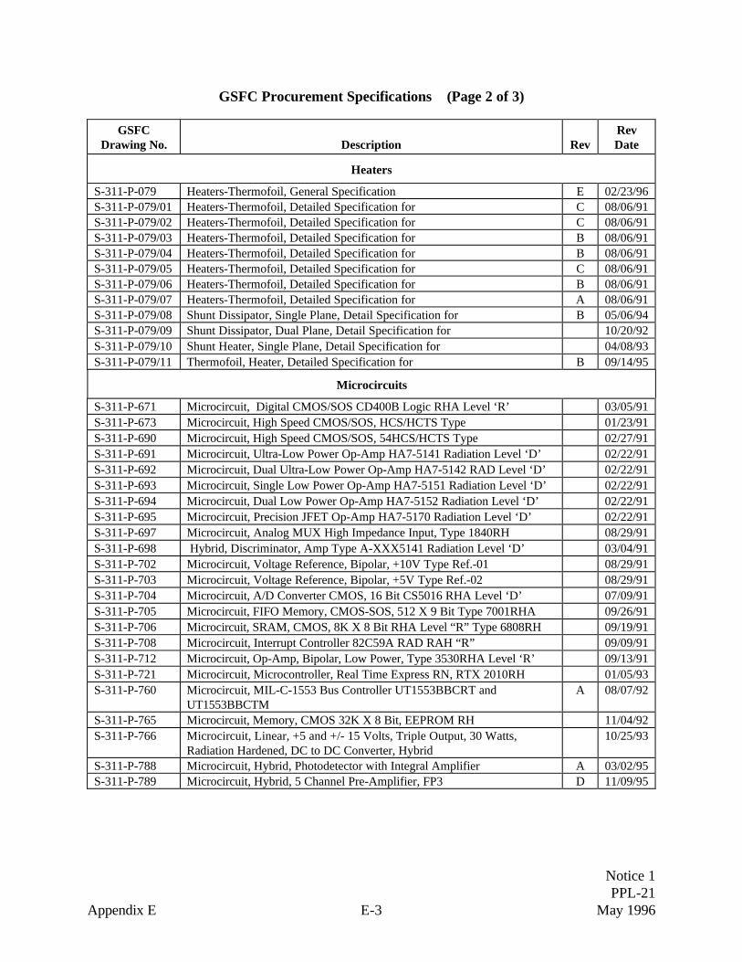
Notice 1PPL-21
Appendix E E-3 May 1996
GSFC Procurement Specifications (Page 2 of 3)
GSFCDrawing No. Description Rev
RevDate
Heaters
S-311-P-079 Heaters-Thermofoil, General Specification E 02/23/96S-311-P-079/01 Heaters-Thermofoil, Detailed Specification for C 08/06/91S-311-P-079/02 Heaters-Thermofoil, Detailed Specification for C 08/06/91S-311-P-079/03 Heaters-Thermofoil, Detailed Specification for B 08/06/91S-311-P-079/04 Heaters-Thermofoil, Detailed Specification for B 08/06/91S-311-P-079/05 Heaters-Thermofoil, Detailed Specification for C 08/06/91S-311-P-079/06 Heaters-Thermofoil, Detailed Specification for B 08/06/91S-311-P-079/07 Heaters-Thermofoil, Detailed Specification for A 08/06/91S-311-P-079/08 Shunt Dissipator, Single Plane, Detail Specification for B 05/06/94S-311-P-079/09 Shunt Dissipator, Dual Plane, Detail Specification for 10/20/92S-311-P-079/10 Shunt Heater, Single Plane, Detail Specification for 04/08/93S-311-P-079/11 Thermofoil, Heater, Detailed Specification for B 09/14/95
Microcircuits
S-311-P-671 Microcircuit, Digital CMOS/SOS CD400B Logic RHA Level ‘R’ 03/05/91S-311-P-673 Microcircuit, High Speed CMOS/SOS, HCS/HCTS Type 01/23/91S-311-P-690 Microcircuit, High Speed CMOS/SOS, 54HCS/HCTS Type 02/27/91S-311-P-691 Microcircuit, Ultra-Low Power Op-Amp HA7-5141 Radiation Level ‘D’ 02/22/91S-311-P-692 Microcircuit, Dual Ultra-Low Power Op-Amp HA7-5142 RAD Level ‘D’ 02/22/91S-311-P-693 Microcircuit, Single Low Power Op-Amp HA7-5151 Radiation Level ‘D’ 02/22/91S-311-P-694 Microcircuit, Dual Low Power Op-Amp HA7-5152 Radiation Level ‘D’ 02/22/91S-311-P-695 Microcircuit, Precision JFET Op-Amp HA7-5170 Radiation Level ‘D’ 02/22/91S-311-P-697 Microcircuit, Analog MUX High Impedance Input, Type 1840RH 08/29/91S-311-P-698 Hybrid, Discriminator, Amp Type A-XXX5141 Radiation Level ‘D’ 03/04/91S-311-P-702 Microcircuit, Voltage Reference, Bipolar, +10V Type Ref.-01 08/29/91S-311-P-703 Microcircuit, Voltage Reference, Bipolar, +5V Type Ref.-02 08/29/91S-311-P-704 Microcircuit, A/D Converter CMOS, 16 Bit CS5016 RHA Level ‘D’ 07/09/91S-311-P-705 Microcircuit, FIFO Memory, CMOS-SOS, 512 X 9 Bit Type 7001RHA 09/26/91S-311-P-706 Microcircuit, SRAM, CMOS, 8K X 8 Bit RHA Level “R” Type 6808RH 09/19/91S-311-P-708 Microcircuit, Interrupt Controller 82C59A RAD RAH “R” 09/09/91S-311-P-712 Microcircuit, Op-Amp, Bipolar, Low Power, Type 3530RHA Level ‘R’ 09/13/91S-311-P-721 Microcircuit, Microcontroller, Real Time Express RN, RTX 2010RH 01/05/93S-311-P-760 Microcircuit, MIL-C-1553 Bus Controller UT1553BBCRT and
UT1553BBCTMA 08/07/92
S-311-P-765 Microcircuit, Memory, CMOS 32K X 8 Bit, EEPROM RH 11/04/92S-311-P-766 Microcircuit, Linear, +5 and +/- 15 Volts, Triple Output, 30 Watts,
Radiation Hardened, DC to DC Converter, Hybrid 10/25/93
S-311-P-788 Microcircuit, Hybrid, Photodetector with Integral Amplifier A 03/02/95S-311-P-789 Microcircuit, Hybrid, 5 Channel Pre-Amplifier, FP3 D 11/09/95

Notice 1PPL-21
Appendix E E-4 May 1996
GSFC Procurement Specifications (Page 3 of 3)
GSFCDrawing No. Description Rev
RevDate
Resistors
S-311-P-741 Resistor, Fixed, Low TC, Precision, High Voltage 05/10/91S-311-P-794 Resistor, Fixed, Low TC, Precision, High Stability A 11/02/95S-311-P-795 Resistor, Fixed, Foil, Precision, Power, Current Sensing, Hermetic A 10/10/95S-311-P-796 Resistor, “Matched-Pair”, Low TC, Precision, Radial-Lead A 1/19/96S-311-P-798 Potentiometer, Precision Trimming, Vishay 128G 08/15/95
Thermistors
S-311-424 Thermistor, Thermally Sensitive, Negative TC, Super Stable,Encapsulated
B 03/21/88
S-311-P-767 Thermistor, Hermetically Sealed, Cryogenic, Negative Temperature,Coefficient, Specification for
A 10/12/93
Transistors
S-311-112 Transistor, Photo Detector, NPN 01/25/83S-311-315 Transistor, JFET, Low Noise ( GMP843) 02/06/84S-311-P-781 Dual N-Channel JFET, Matched Pair. (NJ3600) B 03/02/95
Switches
S-311-641 Switches, Thermostatic, General Specification 09/20/90S-311-641/01 Switches, Thermostatic (Bimetallic), Subminiature, Sealed A 03/23/94
Wire/Cable
S-311-P-71 Wire/Cable, Special Purpose, Twin Conductor Shielded and Jacketed A 10/29/90