Precursor Chemistry for Semiconducting Materials
30
Precursor Chemistry for Main Group Elements in Semiconducting Materials Mohammad Azad Malik, Mohammad Afzaal, and Paul O’Brien* School of Chemistry and Manchester Materials Science Centre, The University of Manchester, Oxford Road, Manchester, M13 9PL, United Kingdom Received December 17, 2009 Contents 1. Introduction 4417 2. Precursor Requirements 4418 3. Precursors for II-VI Materials 4418 3.1. Precursors for II-VI Thin Films 4418 3.1.1. Alternate Chalcogenide Precursors 4419 3.1.2. Adducts of Metal Alkyls 4419 3.1.3. Single-Molecule Precursors 4419 3.2. Precursors for II-VI Nanoparticles 4425 4. Precursors for III-V Materials 4428 4.1. Precursors for III-V Thin Films 4428 4.1.1. Alternative Group V Sources 4428 4.1.2. III-V Adducts 4429 4.1.3. III Nitrides 4429 4.1.4. III Phosphides and Arsenides 4430 4.1.5. III Antimonides 4431 4.2. Precursors for III-V Nanoparticles 4431 5. Precursors for III-VI Materials 4432 5.1. Precursors for III-VI Thin Films 4432 5.1.1. Thiolato Complexes 4432 5.1.2. Thiocarbamato Complexes 4433 5.1.3. Xanthato and Monothiocarbamato Complexes 4433 5.1.4. Dichalcogenoimidodiphosphinato Complexes 4433 5.2. Precursors for III-VI Nanoparticles 4434 6. Precursors for IV-VI Materials 4434 6.1. Precursors for IV-VI Thin Films 4434 6.2. Precursors for IV-VI Nanoparticles 4437 7. Precursors for V-VI Materials 4437 7.1. Precursors for V-VI Thin Films 4437 7.2. Precursors for V-VI Nanoparticles 4440 8. Conclusions 4441 9. Acknowledgments 4442 10. References 4442 1. Introduction The birth of the modern electronics industry can be traced to the invention of the first transistor by Shockley, Brattain, and Bardeen at Bell Laboratories in 1948. This transistor was based on a semiconducting layer of germanium on quartz, and they received the Nobel Prize in Physics in 1956. The integrated monolithic silicon chip (the integrated circuit, IC) was probably the next major breakthrough, for which Jack Kilby of Texas Instruments was awarded a Nobel Prize in 2000. Indeed, silicon continues to dominate the micro- electronics industry. However, compound semiconductors such as gallium arsenide (GaAs) have some electronic properties which are superior to those of silicon. GaAs has a higher saturated electron velocity and higher electron mobility, allowing transistors made from it to function at frequencies in excess of 25 GHz. Also, GaAs devices generate less noise than do those of silicon devices when operated at high frequencies. They operate at higher power levels than the equivalent silicon devices because they have higher breakdown voltages. Another advantage is a direct band gap, a common advantage of compound semiconducting materials, which leads to more efficient optoeclectronic behavior, especially the emission and absorption of photons. Compound semiconductors based on combinations of elements from Groups II and VI, III and V, III and VI, and IV and VI have had a significant impact on our everyday lives. Materials such as GaAs, aluminum gallium arsenide (AlGaAs), gallium nitride (GaN), indium phosphide (InP), zinc selenide (ZnSe), cadmium telluride (CdTe), and copper indium gallium selenide CuInGaSe (CIGS) have a wide variety of applications in satellite TV receivers, optical fiber communications, compact disk players, barcode readers, full color advertising displays, and solar cells. These semicon- ductors are at present generally useful in the form of thin films, but nanoparticles and solids are important with a great future predicted for nanoparticles and perhaps most especially quantum dots. The most common chemistry-based method to thin films is chemical vapor deposition (CVD). Manasevit was the first to grow such thin films (GaAs) in 1968 by the molecular organic (MO) CVD method. 1 These techniques now employ metal-organic compounds of high purity. As the complexity of electronic devices increases, the suit of materials on which diversity is written increases; the demand for elegant precursors decomposing cleanly at lower tem- perature often to deliver complex phases is ever increasing. The most important factor which effects the composition and structure of the deposited material is the nature and purity of the precursors. In CVD processes, molecular precursors must shed the ligands that contributed to their volatility in order to produce a film of a solid-state material. Thermal decomposition of a precursor is the key step which produces a thin film, and ideally the ligands associated with the precursor are cleanly lost into the gas phase. However, that is not often the case, and when complex ligands are involved (heteroleptic compounds), more complex fragmentation takes place. A rational development of precursors for a specific application is thus only possible on the basis of some insights into the molecular decomposition pathways. Study on the precursor decomposition mechanism, in principle, needs to be carried out in the gas phase of the molecules directly, * To whom correspondence should be addressed. Phone: 0161 275 4652. Fax: 0161 275 4616. E-mail: [email protected]. Chem. Rev. 2010, 110, 4417–4446 4417 10.1021/cr900406f 2010 American Chemical Society Published on Web 05/19/2010
-
Upload
sathieshwar -
Category
Documents
-
view
350 -
download
2
Transcript of Precursor Chemistry for Semiconducting Materials

Precursor Chemistry for Main Group Elements in Semiconducting Materials
Mohammad Azad Malik, Mohammad Afzaal, and Paul O’Brien*
School of Chemistry and Manchester Materials Science Centre, The University of Manchester, Oxford Road, Manchester, M13 9PL, United Kingdom
Received December 17, 2009
Contents
1. Introduction 44172. Precursor Requirements 44183. Precursors for II-VI Materials 4418
3.1. Precursors for II-VI Thin Films 44183.1.1. Alternate Chalcogenide Precursors 44193.1.2. Adducts of Metal Alkyls 44193.1.3. Single-Molecule Precursors 4419
3.2. Precursors for II-VI Nanoparticles 44254. Precursors for III-V Materials 4428
4.1. Precursors for III-V Thin Films 44284.1.1. Alternative Group V Sources 44284.1.2. III-V Adducts 44294.1.3. III Nitrides 44294.1.4. III Phosphides and Arsenides 44304.1.5. III Antimonides 4431
4.2. Precursors for III-V Nanoparticles 44315. Precursors for III-VI Materials 4432
5.1. Precursors for III-VI Thin Films 44325.1.1. Thiolato Complexes 44325.1.2. Thiocarbamato Complexes 44335.1.3. Xanthato and Monothiocarbamato
Complexes4433
5.1.4. DichalcogenoimidodiphosphinatoComplexes
4433
5.2. Precursors for III-VI Nanoparticles 44346. Precursors for IV-VI Materials 4434
6.1. Precursors for IV-VI Thin Films 44346.2. Precursors for IV-VI Nanoparticles 4437
7. Precursors for V-VI Materials 44377.1. Precursors for V-VI Thin Films 44377.2. Precursors for V-VI Nanoparticles 4440
8. Conclusions 44419. Acknowledgments 4442
10. References 4442
1. IntroductionThe birth of the modern electronics industry can be traced
to the invention of the first transistor by Shockley, Brattain,and Bardeen at Bell Laboratories in 1948. This transistorwas based on a semiconducting layer of germanium onquartz, and they received the Nobel Prize in Physics in 1956.The integrated monolithic silicon chip (the integrated circuit,IC) was probably the next major breakthrough, for whichJack Kilby of Texas Instruments was awarded a Nobel Prize
in 2000. Indeed, silicon continues to dominate the micro-electronics industry.
However, compound semiconductors such as galliumarsenide (GaAs) have some electronic properties which aresuperior to those of silicon. GaAs has a higher saturatedelectron velocity and higher electron mobility, allowingtransistors made from it to function at frequencies in excessof 25 GHz. Also, GaAs devices generate less noise than dothose of silicon devices when operated at high frequencies.They operate at higher power levels than the equivalentsilicon devices because they have higher breakdown voltages.Another advantage is a direct band gap, a common advantageof compound semiconducting materials, which leads to moreefficient optoeclectronic behavior, especially the emissionand absorption of photons.
Compound semiconductors based on combinations ofelements from Groups II and VI, III and V, III and VI, andIV and VI have had a significant impact on our everydaylives. Materials such as GaAs, aluminum gallium arsenide(AlGaAs), gallium nitride (GaN), indium phosphide (InP),zinc selenide (ZnSe), cadmium telluride (CdTe), and copperindium gallium selenide CuInGaSe (CIGS) have a widevariety of applications in satellite TV receivers, optical fibercommunications, compact disk players, barcode readers, fullcolor advertising displays, and solar cells. These semicon-ductors are at present generally useful in the form of thinfilms, but nanoparticles and solids are important with a greatfuture predicted for nanoparticles and perhaps most especiallyquantum dots. The most common chemistry-based methodto thin films is chemical vapor deposition (CVD). Manasevitwas the first to grow such thin films (GaAs) in 1968 by themolecular organic (MO) CVD method.1 These techniquesnow employ metal-organic compounds of high purity. Asthe complexity of electronic devices increases, the suit ofmaterials on which diversity is written increases; the demandfor elegant precursors decomposing cleanly at lower tem-perature often to deliver complex phases is ever increasing.
The most important factor which effects the compositionand structure of the deposited material is the nature and purityof the precursors. In CVD processes, molecular precursorsmust shed the ligands that contributed to their volatility inorder to produce a film of a solid-state material. Thermaldecomposition of a precursor is the key step which producesa thin film, and ideally the ligands associated with theprecursor are cleanly lost into the gas phase. However, thatis not often the case, and when complex ligands are involved(heteroleptic compounds), more complex fragmentation takesplace. A rational development of precursors for a specificapplication is thus only possible on the basis of some insightsinto the molecular decomposition pathways. Study on theprecursor decomposition mechanism, in principle, needs tobe carried out in the gas phase of the molecules directly,
* To whom correspondence should be addressed. Phone: 0161 275 4652.Fax: 0161 275 4616. E-mail: [email protected].
Chem. Rev. 2010, 110, 4417–4446 4417
10.1021/cr900406f 2010 American Chemical SocietyPublished on Web 05/19/2010
and subsequently surface reactions of the precursors orrelevant fragments have to be investigated. It is interestingto know how a metal complex decomposes by applicationof thermal energy. Detailed gas-phase/surface studies are verycomplex and can only be carried out online.
We have, for several years, been developing single-sourceprecursors (SSPs) for thin films and nanocrystals. The useof SSPs can potentially provide several key advantages overother routes. For example, the existence of preformed bondscan lead to a material with fewer defects and/or betterstoichiometry. In the case of thin film deposition by CVD,conditions of flow and temperature become simpler. It is alsopossible to carry out deposition with relatively simpleinstallations. Several of the SSP are also air stable andtherefore easier to handle and characterize. Systematic studiescomparing the performance of precursors in similar condi-tions remain scarce. This review will highlight some relevantexamples of relationships between precursors and materialsdeposited and discuss the advances made in the design andpreparation of precursors involving main group elements and
their use for synthesis of semiconducting materials in theform of thin films and nanoparticles.
2. Precursor RequirementsThe most important requirement for a precursor is its purity
to prevent contamination of the deposited material and otherundesirable side products. Purification techniques and meth-ods during precursor preparation or possible alternativeprecursor preparation methods are therefore very important.A precursor is also required to decompose at elevatedtemperatures on the substrate surface to give the desired thinfilm. For low-pressure (LP) CVD volatility is a requirement.It is desirable for a precursor to be readily volatile at atemperature well below that of its decomposition. However,due to developments in CVD systems, e.g., aerosol-assisted(AA) CVD and liquid-injection (LI) CVD, this is no longercrucial. The precursor is also required to be stable and havea low degree of toxicity for easy use and storage. Ultimatly,precursor must be able to be synthesized in quantities of atleast several grams with as few synthetic steps as possible.The synthesis must be adaptable to larger scale productionwithout major problems including cost and environmentalimpact.
3. Precursors for II-VI Materials
3.1. Precursors for II-VI Thin FilmsThe growth of II-VI thin films by a chemical method
became practical with Manasevit’s use of volatile metalalkyls such as dimethylcadmium (Me2Cd) or dimethylzinc(Me2Zn) in a combination with H2S, H2Se, or Me2Tedelivered in dihydrogen1 as a carrier gas, effectively inventingand defining the process of MOCVD. Many films weregrown including ZnS, ZnSe, CdS, CdSe, and CdTe.1
Mohammad Azad Malik completed his Ph.D. degree at the University ofLondon in 1990 and since then has been working with Professor PaulO’Brien initially at Queen Mary University of London (1990-1995), thenImperial College (1995-2000), and currently The University of Manchester(2000 to current). He has been involved in various projects and has awide range of experience including single-source molecular precursorsfor II/VI, III/V, III/VI, and IV/VI semiconductors, MOCVD, AACVD, CBD,and the colloidal synthesis of nanoparticles.
Mohammad Afzaal graduated from Aston University, Birmingham, in 2000and moved to the University of Manchester to carry out his Ph.D. studieswith Professor Paul O’Brien, studying growth of semiconductor thin filmsusing single-source precursors. After completing his Ph.D. degree in 2003,he remained with Professor Paul O’Brien and took his current postdoctoralposition, studying nanoparticles and thin film deposition for variousapplications.
Paul O’Brien is Professor of Inorganic Materials Chemistry in the Schoolof Chemistry and the School of Materials at the University of Manchester.He was Head of the School of Chemistry from 2002 to 2009 and ResearchDean from 2000 to 2002. He graduated from Liverpool University in 1975,obtained his Ph.D. degree from the University of Wales, Cardiff, in 1978,and was immediately appointed as a lecturer at Chelsea College of Scienceand Technology, University of London. He moved to Queen Mary andWestfield College in 1984 and was promoted to a chair in 1994. In 1995,he moved to Imperial College and became the Sumitomo/STS Professorof Materials Chemistry (1997-2003). He was Regents appointed VisitingProfessor at the Georgia Institute of Technology (1996-1999). He is aFellow of the Institute of Materials, Minerals, and Mining (FIMMM) and aChartered Engineer (C. Eng). He received the 2007 Kroll Medal from theIOMMM and the first Peter Day Award for Materials Chemistry from theRSC in 2009. In 2006 he was awarded the first ever honorary D.Sc.degree of the University of Zululand, South Africa.
4418 Chemical Reviews, 2010, Vol. 110, No. 7 Malik et al.
The method involves the delivery of both a metal alkyland a chalcogenide source in the vapor phase to a mixingchamber and onward to a deposition zone; particulatematerial can form before the vapors reach the heatedsubstrate, sometimes termed ‘prereaction’. To overcomesome of these problems, new precursors were developed tocontrol volatility, reduce toxic hazard, improve the qualityof the grown layers, and reduce the temperature requiredfor growth. These precursors include alternate chalcogenideprecursors, metal alkyls adducts, and single-source precursors.
3.1.1. Alternate Chalcogenide Precursors
Alkyl chacogenides can be used as alternative chalcogensources to the hydrides. MeSeH,2 Et2Se,3,4 tBuSeH,5 andtBu2Se6 have been used but require higher depositiontemperatures due to their thermal stability. Similarly, di-alkyltellurides, alkylally1tellurides, and diallyltellurides havebeen used7 but cannot be stored longer than a few days dueto their lack of stability.8 A detailed investigation of thedecomposition mechanism of tellurium precursors has un-derlined the importance of homolytic Te-C bond scissionand the role of surface-bound alkyl or ally1 radicals duringfilm growth.9 The formation of radicals in R2Te/CdMe2
mixtures has been shown to lead to alkyl group scrambling,e.g., iPr2Te can be partly converted to thermally more stable(and hence less suitable) derivatives such as Me2Te2 andMeTeiPr. The detailed chemistry of alkyl chalcogenideprecursors has been described in several reviews.10-14
3.1.2. Adducts of Metal Alkyls
Suppression of the homogeneous reaction in the systemMe2Zn/H2Se/pyridine at pyridine to Zn ratios as low as 0.05:115 suggests that the Lewis base does not directly protectthe metal dialkyls but may do so via intermediates such as[MeM(SH)]n. The alkyls of group 12 are weak Lewis acidswith Lewis acidity decreasing in the sequence Zn > Cd >Hg. Replacement of alkyl groups with sulfur, which is a moreelectronegative element, increases the Lewis acidity at themetal and hence its tendency to bind additional ligands orform aggregates of higher nuclearity.
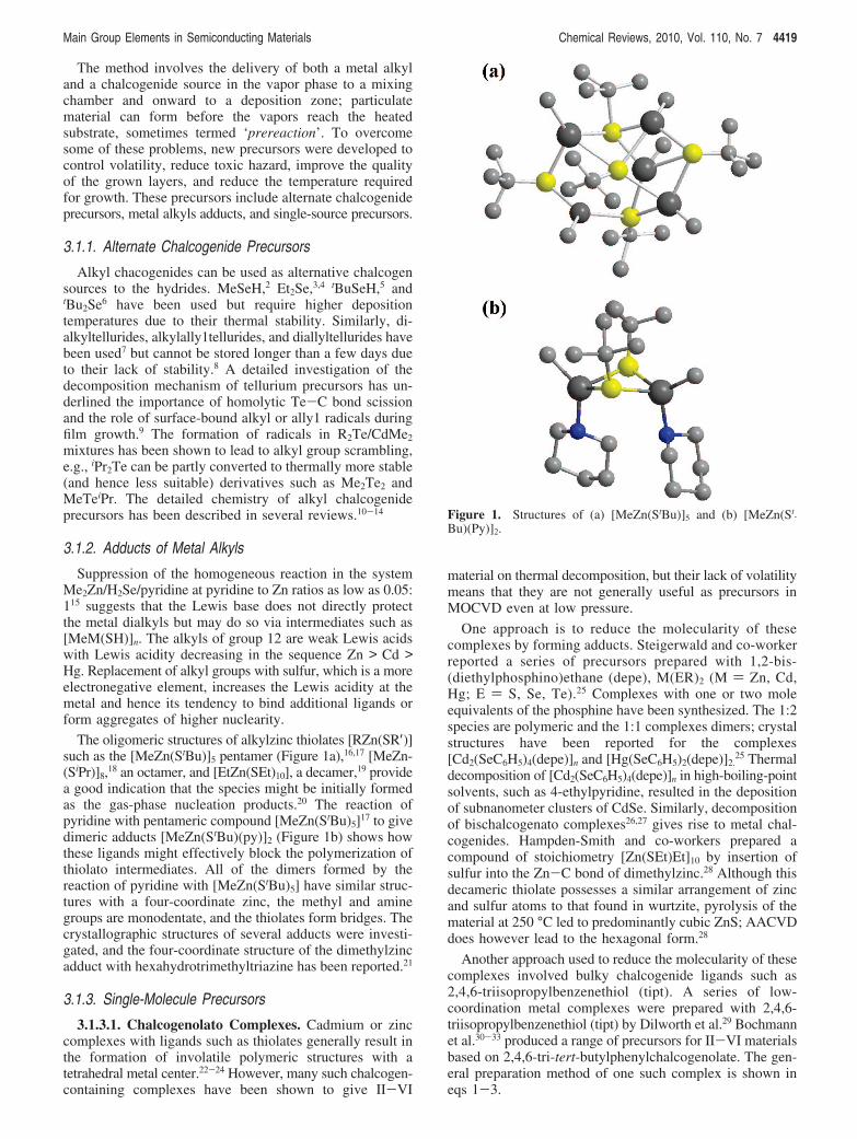
The oligomeric structures of alkylzinc thiolates [RZn(SR′)]such as the [MeZn(StBu)]5 pentamer (Figure 1a),16,17 [MeZn-(SiPr)]8,18 an octamer, and [EtZn(SEt)10], a decamer,19 providea good indication that the species might be initially formedas the gas-phase nucleation products.20 The reaction ofpyridine with pentameric compound [MeZn(StBu)5]17 to givedimeric adducts [MeZn(StBu)(py)]2 (Figure 1b) shows howthese ligands might effectively block the polymerization ofthiolato intermediates. All of the dimers formed by thereaction of pyridine with [MeZn(StBu)5] have similar struc-tures with a four-coordinate zinc, the methyl and aminegroups are monodentate, and the thiolates form bridges. Thecrystallographic structures of several adducts were investi-gated, and the four-coordinate structure of the dimethylzincadduct with hexahydrotrimethyltriazine has been reported.21
3.1.3. Single-Molecule Precursors
3.1.3.1. Chalcogenolato Complexes. Cadmium or zinccomplexes with ligands such as thiolates generally result inthe formation of involatile polymeric structures with atetrahedral metal center.22-24 However, many such chalcogen-containing complexes have been shown to give II-VI
material on thermal decomposition, but their lack of volatilitymeans that they are not generally useful as precursors inMOCVD even at low pressure.
One approach is to reduce the molecularity of thesecomplexes by forming adducts. Steigerwald and co-workerreported a series of precursors prepared with 1,2-bis-(diethylphosphino)ethane (depe), M(ER)2 (M ) Zn, Cd,Hg; E ) S, Se, Te).25 Complexes with one or two moleequivalents of the phosphine have been synthesized. The 1:2species are polymeric and the 1:1 complexes dimers; crystalstructures have been reported for the complexes[Cd2(SeC6H5)4(depe)]n and [Hg(SeC6H5)2(depe)]2.
25 Thermaldecomposition of [Cd2(SeC6H5)4(depe)]n in high-boiling-pointsolvents, such as 4-ethylpyridine, resulted in the depositionof subnanometer clusters of CdSe. Similarly, decompositionof bischalcogenato complexes26,27 gives rise to metal chal-cogenides. Hampden-Smith and co-workers prepared acompound of stoichiometry [Zn(SEt)Et]10 by insertion ofsulfur into the Zn-C bond of dimethylzinc.28 Although thisdecameric thiolate possesses a similar arrangement of zincand sulfur atoms to that found in wurtzite, pyrolysis of thematerial at 250 °C led to predominantly cubic ZnS; AACVDdoes however lead to the hexagonal form.28
Another approach used to reduce the molecularity of thesecomplexes involved bulky chalcogenide ligands such as2,4,6-triisopropylbenzenethiol (tipt). A series of low-coordination metal complexes were prepared with 2,4,6-triisopropylbenzenethiol (tipt) by Dilworth et al.29 Bochmannet al.30-33 produced a range of precursors for II-VI materialsbased on 2,4,6-tri-tert-butylphenylchalcogenolate. The gen-eral preparation method of one such complex is shown ineqs 1-3.
Figure 1. Structures of (a) [MeZn(StBu)]5 and (b) [MeZn(St-
Bu)(Py)]2.
Main Group Elements in Semiconducting Materials Chemical Reviews, 2010, Vol. 110, No. 7 4419

The compounds are dimeric, even in the vapor phase, andcan be used in LP-MOCVD for the deposition of II-VImaterials.34,35 For example, [Cd(SC6H2
tBu3-2,4,6)]2 gavepolycrystalline CdS thin films at a substrate temperature of450 °C (10-2 Torr). The mercury analogues readily decom-posed via a reductive elimination path to form atomic Hgand diary1dichalcogenides, which may indicate that thesecompounds are more suitable for the photoassisted ratherthan the thermal MOCVD method.32 Organometallic chal-cogenates36 with aryl chalcogenates RMSeR′ (R′ ) C6H2
iPr3-2,4,6; M ) Zn, R ) Me, Et, Pr, iPr; M ) Cd, R ) Me)have also been prepared but have not to date been evaluatedfor thin film studies.
A series of related precursors are silicon-based systemsof stoichiometry M[ESi(SiMe)3]2 (M ) Zn, Cd, Hg; E ) S,Se, or Te) as devised by Arnold and co-workers to deposita range of chalcogenides.37,38 The most detailed work wasreported on the tellurides: thin films of the tellurides havebeen deposited by LP-MOCVD.39 The tellurium-containingligand HTeSi(SiMe3)3 is termed HSitel, and this reagent ispotentially useful in the preparation of metal tellurolates.40-42
Metal complexes of Site1 are generally prepared as illustratedbelow, eq 4.
ZnTe was deposited at temperatures between 250 and 350°C onto quartz, Si, InAs, and GaSb substrates. The cadmiumprecursor gave hexagonal material with a better stoichiometrythan those of ZnTe.
3.1.3.2. Dithio-/Diselenophosphinato Complexes. Inearly work, Takahashi43 deposited CdS using dimethylthio-phosphinates [M(S2PMe2)2] (M ) Cd or Zn) and Evans andWilliams reported44 that highly orientated CdS films couldbe grown using the diethyldithiophosphinates as precursors.
CdS and ZnS films have been deposited from[Cd(S2PiBu2)2]2 and [Zn(S2PiBu2)2]2, respectively, using ahomemade cold-wall low-pressure reactor.45 The cadmiumcomplex has a classic Ci-symmetric two-step ladder (or“chair”) structure (Figure 2) of type 23 for the central eight-membered Cd2S4P2 ring.46 This geometry contrasts with theC2-symmetric “boat” conformation observed for the closelyrelated isopropoxide complex Cd2[(i-C3H7O)2PS2]4.47 X-rayanalysis of the zinc complex shows it to adopt a geometryfor the Zn2S8P4 core that is virtually identical with that seenin the cadmium and zinc complexes with O,O-diisopropy-lphosphordithioate.47
A series of metal complexes of bis(dialkylselenophosphi-nyl)selenide [(R2PSe2)Se] (R ) Ph, iPr) with the generalformula [M(R2PSe2)n] (M ) Zn, Cd, Pb, In, Ga, Cu, Bi, Ni;R ) iPr, Ph) and [Mo2O2Se2(Se2PiPr2)2] have been synthe-sized and used for the growth of metal selenide thin filmsby CVD.48,49 The ligands [(R2PSe2)2Se] (R ) iPr, Ph) wereprepared from the reaction of NEt3 with Ph2PCl oriPr2PCland HSiCl3 in cold toluene (eqs 5 and 6).
Reaction with different metal salts was then carried outin methanolic solutions and gave the metal complexes asprecipitates, which were subsequently recrystallized fromdichloromethane or toluene. Indium forms (Figure 3a), asexpected, the [In(iPr2PSe2)3] complex. All three diseleno-phosphinate ligands are chelating to form four-memberedrings (Se-P-Se-In) with In-Se bond distances that rangefrom 2.729(6) to 2.768(6) Å. The geometry at indium istrigonally-distorted octahedral due to the restricted bite angleof the chelating diselenophosphinate ligand.
The structure of [Ga(iPr2PSe2)3] (Figure 3b) has a four-coordinate gallium center, in contrast to the six-coordinateindium. Until recently,50 all reports on structurally character-ized pairs of analogues In/Ga tris (chelates) with (O, O′) or(S, S′) ligands have been shown to be isostructural.51,52 Thefirst such four-coordinate structure for a gallium complexwas tris(diisobutyldithiophophinato)gallium([Ga(Ph2PS2)3]53
with one chelating and two pendant diisopropyldiseleno-phosphinate ligands in a distorted tetragonal geometry. Thephenyl analogue [Ga(Ph2PSe2)3]48 showed a similar coordi-nation pattern.
3.1.3.3. Bis(dialkydithio/selenocarbamato)metal Spe-cies. Dialkyldithio/diselenocarbamato metal complexeswith the general formula [(M(E2CNR2)2] (symmetrical)or [M(E2CNRR′)2] (unsymmetrical) (R, R′ ) alkyl, E ) S,Se; M ) Zn, Cd) are precursors that have been used for thedeposition of II-VI thin films. All of these compounds are
M[N(SiMe3)2]2 + 2HTeSi(SiMe3)3 f
[MTeSi(SiMe3)32]2(s) + 2HN(SiMe3)2
M ) Zn, Cd, Hg(4)
Figure 2. Molecular structure of [Cd(S2PiBu2)2]2 showing its“chair” conformation.
R2PCl + HSiCl3 + NEt398toluene
6h, rtR2PSiCl3 + (HNEt3)Cl
(5)
R2PSiCl3 + 3Se98toluene
20h, reflux(R2PSe2)2Se + Si2Cl6
(6)
4420 Chemical Reviews, 2010, Vol. 110, No. 7 Malik et al.

stable crystalline solids with some volatility. Their solid-state structures have been determined by X-ray crystal-lography. Most of them, including [Zn(S2CNR2)2] (R ) Me,Et, or iPr),54-56 [Cd(S2CNEt2)2] (Figure 4), [Zn(Se2CNEt2)2],[Cd(Se2CNEt2)2], and [Zn(S2CNMeR)2] (R ) Et, nPr, iPr,or nBu), have dimeric structures.57-60 Saunders et al.61 werethe first to use diethyldithiocarbamates [M(S2CNEt2)2] (M) Cd, Zn) for the deposition of ZnS, CdS, and ZnxCd1-xSthin films by the LP-MOCVD method. The same precursorswere used to grow heterostructures by organometallic vapor-
phase epitaxy (OMVPE).62,63 Frigo et al. deposited good-quality CdS or ZnxCd1-xS films prepared from an equimolarmixture of the precursors [Zn(S2CNEt2)2] and [Cd(S2CNEt2)2]on (100)-oriented GaAs or InP substrates64 by LP-MOCVD.The quality of ZnS films deposited from [Zn(S2CNEt2)2] waspoor.
Deposition by MOCVD of ZnS usually gives the hexago-nal, R-ZnS, wurtzite, but Nomura et al. deposited the cubic,-ZnS, zinc blende epitaxially on (111)-Si by OMVPE using[Zn(S2CNEt2)2] in a cold-wall horizontal reactor.65 It wasobserved that the deposition conducted at low pressure (10-2
Torr) produced hexagonal R-ZnS of poor crystallinity andmorphology, whereas depositions with introduction of acarrier gas (N2) gave good-quality (111)-oriented -ZnS.Fainer et al. used [Cd(S2CNEt2)2] with He or H2 as a carriergas in LP-MOCVD66 and plasma-enhanced MOCVD (PE-MOCVD)67 to grow CdS on SiO2, Al2O3 (sapphire), (111)-Si, and (111)-InP.66
Bis(dialkyldithio/selenocarbamato)cadmium/zinc compoundshave had the advantage of stability for years, but the volatilityof the precursors can be a limiting factor. In addition, forselenides the quality of the films was often poor with elementalselenium contamination. However, air-stable unsymmetricalprecursors based on [M(S2CNRR′)2] (M ) Cd or Zn; RR′ )alkyl groups) decompose cleanly in MOCVD to selenides orsulfides.68-70 Volatilization experiments shown that the unsym-metrically substituted [Zn(S2CNMeEt)]2, [Zn(S2CNMenPr)]2,and [Zn(S2CNMenBu)]2 volatilize well above their meltingpoints, whereas [Zn(S2CNEt2)2]2 sublimes as a solid.60 ZnS filmwas grown on glass from [Zn(S2CNMenBu)]2 by LP-MOCVD at 450 °C in a cold-wall reactor.60 Depositionstudies on [Cd(S2CNEt2)2] and [Cd(S2CNMenBu)2] showedthat the methyl butyl derivative was more volatile71 and thatthe films grown on InP at 500 °C were of polycrystallineCdS.
A series of other unsymmetrical dithio- and diselenocar-bamates has also been synthesized and used as SSPs fordeposition of thin films. Bis(n-hexyl(methyl)dithio/seleno-carbamato)cadmium/zinc (Figure 5) proved to be the bestof the unsymmetrical derivatives for growth of chalo-genides.72
Since dithio- and diselenocarbamates and their derivativeshave been used widely in the deposition of thin films andnanoparticles, a mechanistic study of their decompositionbehavior was carried out by O’Brien et al.70 Wold73 studiedthe decomposition products of [Zn(S2CNEt2)2] using GC-MS, and their reported deposition path shows the clean
Figure 3. Structures of (a) [In(iPr2PSe2)3] and (b) [Ga(iPr2PSe2)3].
Figure 4. Structure of Cd(S2CNEt2)2.
Figure 5. Structure of [Cd(Se2CNMenHex)2]2.
Main Group Elements in Semiconducting Materials Chemical Reviews, 2010, Vol. 110, No. 7 4421

elimination of ZnS from the precursor (eqs 7 and 8 below).However, the proposed decomposition route is somewhatdifferent from the step-by-step fragmentation observed in theEI-MS of the compound (eq 9). This difference can beattributed to inherent differences between the two techniques.
In contrast, the analogous diethyl-diselenocarbamates havebeen shown to be poor sources for deposition of ZnSe orCdSe films. Under similar reaction conditions (10-3-10-4
Torr, 370-420 °C), the diethyl-diselenocarbamates precur-sors give films of the metal selenide heavily contaminatedwith selenium.59 However, the mixed alkyl diselenocarbam-ates complex have been used successfully to deposit thinfilms of CdSe or ZnSe.74,75
ZnSe films were deposited from [Zn(Se2CNMenHex)2],which has two different alkyl substituents at the nitrogen.This complex is monomeric in the solid phase68 (Figure 6),in contrast to the analogous diethyl-diselenocarbamates andthe mixed alkyl-diselenocarbamates complexes, which areboth dimers. All of the dithiocarbamates prepared can beused to deposit CdS or ZnS by MOCVD, but the diseleno-carbamates show a different pattern of behavior;[M(Se2CNEt2)2] (M ) Zn, Cd) deposit films heavily con-taminated with selenium, whereas [M(Se2CNRR′)2] (M )Zn, Cd) and [EtZnSe2CNEt2]2 deposit the metal selenide. Itwas of interest to study the decomposition of the compoundsby GC-MS and EI-MS to determine why the latter aresuccessful precursors and also plausible decompositionpathways for comparison with the dithiocarbamato com-plexes. Plausible schemes for decomposition of the precursorhave been proposed (Scheme 1).
Among several limiting factors in the deposition ofchalcogenides from these compounds is the volatility of thecomplexes which can particularly influence the results of thedeposition. Some attempts to obtain more volatile dithio-
carbamato complexes have been made. The dithiocarbamatocomplexes derived from trimethylpropylenediamine weresynthesized76,77 by a comproportionation reaction. Thiscomplex showed a different structure from the dimers andis a weakly bonded polymer, as shown in Figure 7. Thecompound is apparently more volatile than the simplerdithiocarbamates and has successfully been used in deposi-tion experiments to deposit CdS thin film on glass or GaAssubstrates at 350 °C.76
3.1.3.4. N-Alkyldithiocarbamato Complexes. Anotherrelated class of compounds N-alkyldithiocarbamato[M(S2CNHR)2] has potential as precursors. These complexeshave received scant attraction78 because of a perceived lackof stability and expectation of low volatility. Recently,O’Brien et al.79 synthesized a series of complexes ofcadmium or zinc with varying alkyl chain lengths[M(S2CNHR)2] (M ) Cd, Zn; R ) ethyl, nbutyl, nhexyl,ndodecyl).
Condensation of the primary amines with carbon disulfidein the presence of metal salts produced [M(S2CNHR)2] (M) Cd or Zn) in reasonable purity and with a good yield.Most of these complexes were only sparingly soluble inorganic solvents. The zinc complexes were comparativelystable and more soluble. The compound [Zn(S2CNHHex)2]was recrystallized from dichloromethane to give good-qualitycrystals used for X-ray study (Figure 8).79
The cadmium complexes decomposed to a cadmiumsulfate complex with pyridine and water, which crystallizedfrom pyridine. Stable bis(N-alkyldithiocarbamato) cadmiumcomplexes have been prepared by metathesis between lithiumN-alkyldithiocarbamato salts and cadmium chloride in neutralaqueous solution.80 The N-alkyldithiocarbamato complexesare less stable than their corresponding N,N-dialkyldithio-carbamato complexes due to the presence of the acidichydrogen at the nitrogen.
Thermogravimetric analysis (TGA) was conducted toevaluate the decompositional behavior of the N-alkyldithio-carbamato complexes of cadmium and zinc.79 The cadmiumcompounds decompose in an unresolved two-step mecha-
Figure 6. Structure of [Zn(Se2CNMenHex)2].
Zn(S2CNEt2)2 f ZnS + EtNCS + Et2NCS2Et (7)
Et2NCS2Et f Et2NH + CS2 + C2H4 (8)
Zn(S2CNEt2)298-S2CNEt2
Zn(S2CNEt2)298-SCNEt2
ZnS (9)
Scheme 1. Decomposition Mechanism of Bis(hexyl(methyl)-diselenocarbamato)zinc
Figure 7. Structure of [MeCd(MeN(CH2)3NMe2)]n.
Figure 8. Structure of [Zn(S2CNHHex)2]2.
4422 Chemical Reviews, 2010, Vol. 110, No. 7 Malik et al.
nism. In contrast, the zinc compounds decomposed in a singlestep. It was surprising to note that the decomposition behaviorof the compounds changed as the chain length was increased,indicated by the final residue of compounds. The remainingresidues from [M(S2CNHR)2] (M ) Zn, Cd; R ) nHex,ndodecyl) were very close to the values calculated for bulkmetal sulfide, whereas shorter substituted alkyl chain com-pounds such as ethyl or butyl gave a significantly largerresidue than expected from the stoichiometric ratio, indicatingincomplete decomposition or inclusion of impurities afterdecomposition of precursor.
3.1.3.5. Mixed Alkyl/Dithio- or DiselenocarbamatoComplexes. These compounds were first prepared by Nolt-es81 using an insertion reaction82 (eq 10).
Comproportionation (eq 11) can provide a more convenientroute to these compounds.83-85
The compounds are dimers82 in the solid state, and the parentdimeric structure has been confirmed for a wide range ofcompounds where R ) Me, Et, tBu, or Me3CCH2, M ) Znor Cd, E ) S or Se, R′ ) Me or Et.86,87 X-ray single-crystalstructures of neopentylcadmium and diethyldiselenocarbam-ate are shown in Figure 9a and 9b.88
An interesting application of the comproportionationreaction is the preparation of a mixed species such asmethylcadmium/methylzinc diethyldiselenocarbamate, whichis useful for the deposition of thin films of the ternary solid
solutions of Cd0.5Zn0.5Se. Thus, reaction of Me2Zn with[Cd(Se2CNEt2)2] gave [Me2CdZn(Se2CNEt2)2] as shown ineq 12.
A polycrystalline Cd0.5Zn0.5Se layer with a band gap of 2.1eV, was deposited on a glass substrate by LP-MOCVD (450°C, 0.2 Torr). The mixed compound showed similar dimericmolecular units [RM(Se2CNEt2)]2 to other alkylmetal dithio-and diselenocarbamates. In the solid-state structures, thecadmium and zinc atoms were modeled as randomly oc-cupying the metal sites.75 Many of these mixed alkyldiseleno- and dithiocarbamato compounds have been usedto deposit thin films of metal chalcogenides by LP-MOCVD(10-2-10-3 Torr).
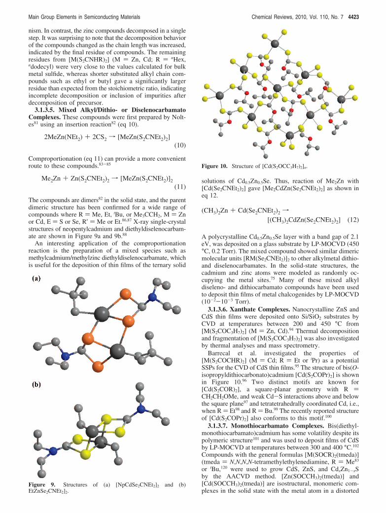
3.1.3.6. Xanthate Complexes. Nanocrystalline ZnS andCdS thin films were deposited onto Si/SiO2 substrates byCVD at temperatures between 200 and 450 °C from[M(S2COC3H7)2] (M ) Zn, Cd).94 Thermal decompositionand fragmentation of [M(S2COC3H7)2] was also investigatedby thermal analyses and mass spectrometry.
Barrecal et al. investigated the properties of[M(S2COCHR)2] (M ) Cd; R ) Et or iPr) as a potentialSSPs for the CVD of CdS thin films.95 The structure of bis(O-isopropyldithiocarbonato)cadmium [Cd(S2COPr)2] is shownin Figure 10.96 Two distinct motifs are known for[Cd(S2COR)2], a square-planar geometry with R )CH2CH2OMe, and weak Cd-S interactions above and belowthe square plane97 and tetratetrahedrally coordinated Cd, i.e.,when R ) Et98 and R ) Bu.99 The recently reported structureof [Cd(S2COPr)2] also conforms to this motif.100
3.1.3.7. Monothiocarbamato Complexes. Bis(diethyl-monothiocarbamato)cadmium has some volatility despite itspolymeric structure101 and was used to deposit films of CdSby LP-MOCVD at temperatures between 300 and 400 °C.102
Compounds with the general formulas [M(SOCR)2(tmeda)](tmeda ) N,N,N,N-tetramethylethylenediamine, R ) Me83
or tBu,120 were used to grow CdS, ZnS, and CdxZn1-xSby the AACVD method. [Zn(SOCCH3)2(tmeda)] and[Cd(SOCCH3)2(tmeda)] are isostructural, monomeric com-plexes in the solid state with the metal atom in a distorted
2MeZn(NEt2) + 2CS2 f [MeZn(S2CNEt2)2](10)
Me2Zn + Zn(S2CNEt2)2 f [MeZn(S2CNEt2)]2
(11)
Figure 9. Structures of (a) [NpCdSe2CNEt2]2 and (b)EtZnSe2CNEt2]2.
Figure 10. Structure of [Cd(S2OCC3H7)2]n.
(CH3)2Zn + Cd(Se2CNEt2)2 f
[(CH3)2CdZn(Se2CNEt2)2] (12)
Main Group Elements in Semiconducting Materials Chemical Reviews, 2010, Vol. 110, No. 7 4423
tetrahedral coordination environment comprising two nitro-gens and two sulfurs.83
3.1.3.8. Dichalcogenoimidodiphosphinato Complexes.The dichalcogenoimidodiphosphinate anions (Figure 11)were first synthesized by Schmidpeter et al. in the 1960s.85
In 1995, Woollins and co-workers initiated the chemistryof the selenium analogue.103 Much of the early developmentof the coordination chemistry of these ligands with both maingroup104 and transition metals104,105 was carried out on thephenyl derivatives. In 2004 it was demonstrated that metalcomplexes incorporating the more volatile isopropyl ligandsare excellent precursors for the production of a variety ofbinary metal selenides.106-108
Imino-diisopropylphosphine selenides are prepared byoxidative insertion of elemental selenium into NH(PiPr2)2.109
The cadmium compound Cd[(SePiPr2)2N]2 (Figure 12) wasfirst synthesized by Woollins et al.109 from diisopropylchlo-rophosphine via a two-step strategy. Improved yields forCd[(SePiPr2)2N]2 above those reported can be afforded byutilizing CdCl2/NaOMe conditions rather than CdCO3 (eqs13-15).
Imino-bis(dialkylphosphine selenide) complexes have beenused in CVD.110,111 The [NH(SePiPr2)2] ligand is morethermally stable than bulky selenolate ligands, such as[SeSi(SiMe3)3]-, and thermolysis of its complexes producescleaner products with reduced contamination caused by undesir-
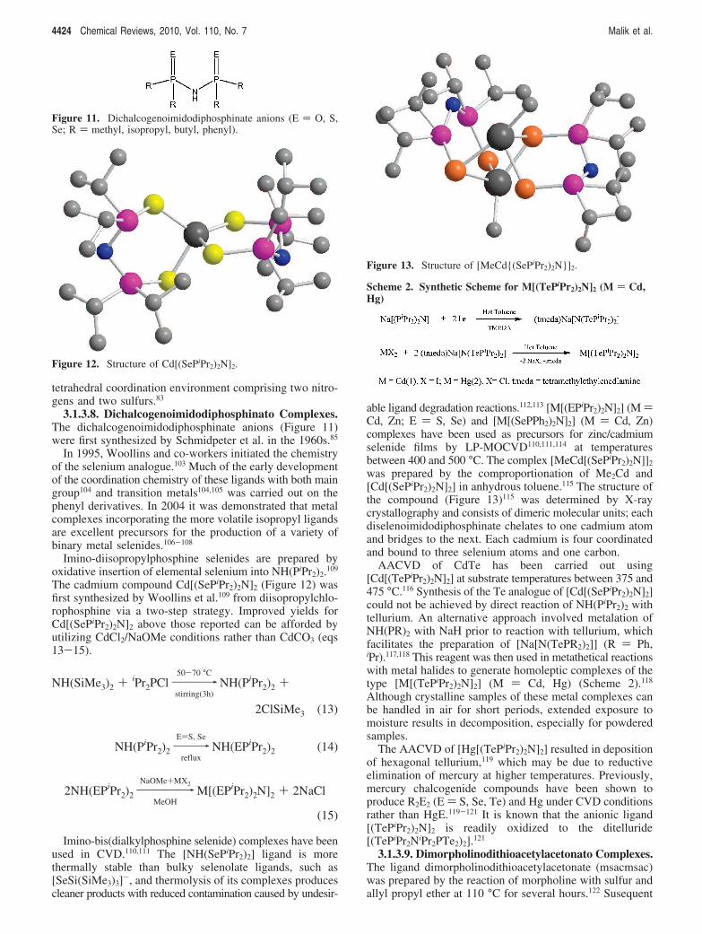
able ligand degradation reactions.112,113 [M[(EPiPr2)2N]2] (M )Cd, Zn; E ) S, Se) and [M[(SePPh2)2N]2] (M ) Cd, Zn)complexes have been used as precursors for zinc/cadmiumselenide films by LP-MOCVD110,111,114 at temperaturesbetween 400 and 500 °C. The complex [MeCd[(SePiPr2)2N]]2
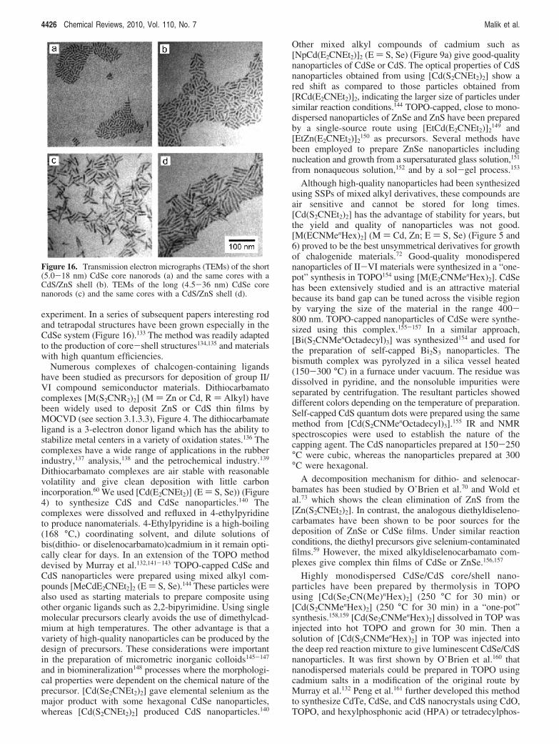
was prepared by the comproportionation of Me2Cd and[Cd[(SePiPr2)2N]2] in anhydrous toluene.115 The structure ofthe compound (Figure 13)115 was determined by X-raycrystallography and consists of dimeric molecular units; eachdiselenoimidodiphosphinate chelates to one cadmium atomand bridges to the next. Each cadmium is four coordinatedand bound to three selenium atoms and one carbon.
AACVD of CdTe has been carried out using[Cd[(TePiPr2)2N]2] at substrate temperatures between 375 and475 °C.116 Synthesis of the Te analogue of [Cd[(SePiPr2)2N]2]could not be achieved by direct reaction of NH(PiPr2)2 withtellurium. An alternative approach involved metalation ofNH(PR)2 with NaH prior to reaction with tellurium, whichfacilitates the preparation of [Na[N(TePR2)2]] (R ) Ph,iPr).117,118 This reagent was then used in metathetical reactionswith metal halides to generate homoleptic complexes of thetype [M[(TePiPr2)2N]2] (M ) Cd, Hg) (Scheme 2).118
Although crystalline samples of these metal complexes canbe handled in air for short periods, extended exposure tomoisture results in decomposition, especially for powderedsamples.
The AACVD of [Hg[(TePiPr2)2N]2] resulted in depositionof hexagonal tellurium,119 which may be due to reductiveelimination of mercury at higher temperatures. Previously,mercury chalcogenide compounds have been shown toproduce R2E2 (E ) S, Se, Te) and Hg under CVD conditionsrather than HgE.119-121 It is known that the anionic ligand[(TePiPr2)2N]2 is readily oxidized to the ditelluride[(TePiPr2NiPr2PTe2)2].121
3.1.3.9. Dimorpholinodithioacetylacetonato Complexes.The ligand dimorpholinodithioacetylacetonate (msacmsac)was prepared by the reaction of morpholine with sulfur andallyl propyl ether at 110 °C for several hours.122 Susequent
Figure 11. Dichalcogenoimidodiphosphinate anions (E ) O, S,Se; R ) methyl, isopropyl, butyl, phenyl).
Figure 12. Structure of Cd[(SePiPr2)2N]2.
NH(SiMe3)2 + iPr2PCl9850-70 °C
stirring(3h)NH(PiPr2)2 +
2ClSiMe3 (13)
NH(PiPr2)298E)S, Se
refluxNH(EPiPr2)2 (14)
2NH(EPiPr2)298NaOMe+MX2
MeOHM[(EPiPr2)2N]2 + 2NaCl
(15)
Figure 13. Structure of [MeCd(SePiPr2)2N]2.
Scheme 2. Synthetic Scheme for M[(TePiPr2)2N]2 (M ) Cd,Hg)
4424 Chemical Reviews, 2010, Vol. 110, No. 7 Malik et al.
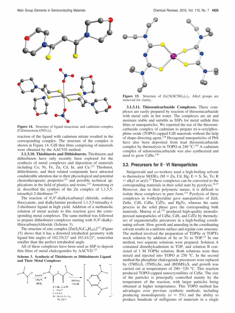
reaction of the ligand with cadmium nitrate resulted in thecorresponding complex. The structure of the complex isshown in Figure 14. CdS thin films comprising of nanorodswere obtained by the AACVD method.
3.1.3.10. Thiobiurets and Dithioburets. Thiobiurets anddithioburets have only recently been explored for thesynthesis of metal complexes and deposition of materialsincluding Co, Ni, Fe, Zn, Cd, In, and Cu.123 Thioburet,dithiobiurets, and their related compounds have attractedcondiderable attention due to their physiological and potentialchemotherapeutic properties124 and possible technical ap-plications in the field of plastics and resins.125 Armstrong etal. described the synthsis of the Zn complex of 1,1,5,5-tetraethyl-2-thiobiuret.126
The reaction of N,N′-dialkylcarbamyl chloride, sodiumthiocyanate, and dialkylamine produced 1,1,5,5-tetraalky-l-2-thiobiuret ligand in high yield. Addition of a methanolicsolution of metal acetate to this reaction gave the corre-sponding metal complexes. The same method was followedto prepare dithiobiuret complexes starting with N,N′-dialky-lthiocarbamylchloride (Scheme 3).
The structure of zinc complex [Zn(S2N3C10H20)2]127 (Figure15) shows that it has a distorted tetrahedral geometry withligand bite angles of 102.55(2)° and 103.41(2)°, somewhatsmaller than the perfect tetrahedral angle.
All of these complexes have been used as SSP to depositthin films of metal chalcogenides by AACVD.127
3.1.3.11. Thiosemicarbazide Complexes. These com-plexes are easily prepared by reaction of thiosemicarbazidewith metal salts in hot water. The complexes are air andmoisture stable and suitable as SSPs for metal sulfide thinfilms or nanoparticles. We reported the use of the thiosemi-carbazide complex of cadmium to prepare tri-n-octylphos-phine oxide (TOPO) capped CdS nanorods without the helpof shape-directing agent.128 Hexagonal nanoparticles of PbShave also been deposited from lead thiosemicarbazidecomplex by thermolysis in TOPO at 240 °C.129 A cadmiumcomplex of selenosemicarbazide was also synthesized andused to grow CdSe.130
3.2. Precursors for II-VI NanoparticlesSteigerwald and co-workers used a high-boiling solvent
to thermolyze M(ER)2 (M ) Zn, Cd, Hg; E ) S, Se, Te; R) alkyl or aryl).25 These complexes can be converted to thecorresponding materials in their solid state by pyrolysis.26,27
However, due to their polymeric nature, it is difficult toisolate these complexes in pure form.131 Pyrolysis of thesecomplexes in 4-ethylpyridine gave nanoparticles of ZnS,ZnSe, CdS, CdSe, CdTe, and HgTe, whereas the sameprocess in the solid phase gave the corresponding bulkmaterials. Murray et al.132 produced high-quality monodis-peresed nanoparticles of CdSe, CdS, and CdTe by thermoly-ses of organometallic precursors in a high-boiling coordi-nating solvent. Slow growth and annealing in the coordinatingsolvent results in a uniform surface and regular core structure.The method involved the preparation of TOPSe or TOPTestock solution by addition of Se or Te to TOP.25 In onemethod, two separate solutions were prepared. Solution Acontained dimethylcadmium in TOP, and solution B con-sisted of 1 M TOPSe solution. Both solutions were thenmixed and injected into TOPO at 250 °C. In the secondmethod the phosphine chalcogenide precursors were replacedby (TMS)2S, (TMS)2Se, and (BDMS)2S, and growth wascarried out at temperatures of 290-320 °C. This reactionproduced TOPO-capped nanocrystallites of CdSe. The sizeof the particles is principally controlled mainly by thetemperature of the reaction, with larger particles beingobtained at higher temperatures. This TOPO method hasadvantages over previous synthetic methods, includingproducing monodispersity (σ ≈ 5%) and the ability toproduce hundreds of milligrams of materials in a single
Figure 14. Structure of ligand msacmsac and cadmium complex[Cd(msacmsac)(NO3)2].
Scheme 3. Synthesis of Thiobiurets or Dithiobiurets Ligandand Their Metal Complexes
Figure 15. Structure of ZnN(SCNEt2)22. Alkyl groups areremoved for clarity.
Main Group Elements in Semiconducting Materials Chemical Reviews, 2010, Vol. 110, No. 7 4425
experiment. In a series of subsequent papers interesting rodand tetrapodal structures have been grown especially in theCdSe system (Figure 16).133 The method was readily adaptedto the production of core-shell structures134,135 and materialswith high quantum efficiencies.
Numerous complexes of chalcogen-containing ligandshave been studied as precursors for deposition of group II/VI compound semiconductor materials. Dithiocarbamatocomplexes [M(S2CNR2)2] (M ) Zn or Cd, R ) Alkyl) havebeen widely used to deposit ZnS or CdS thin films byMOCVD (see section 3.1.3.3), Figure 4. The dithiocarbamateligand is a 3-electron donor ligand which has the ability tostabilize metal centers in a variety of oxidation states.136 Thecomplexes have a wide range of applications in the rubberindustry,137 analysis,138 and the petrochemical industry.139
Dithiocarbamato complexes are air stable with reasonablevolatility and give clean deposition with little carbonincorporation.60 We used [Cd(E2CNEt2)] (E ) S, Se)) (Figure4) to synthesize CdS and CdSe nanoparticles.140 Thecomplexes were dissolved and refluxed in 4-ethylpyridineto produce nanomaterials. 4-Ethylpyridine is a high-boiling(168 °C,) coordinating solvent, and dilute solutions ofbis(dithio- or diselenocarbamato)cadmium in it remain opti-cally clear for days. In an extension of the TOPO methoddevised by Murray et al.132,141-143 TOPO-capped CdSe andCdS nanoparticles were prepared using mixed alkyl com-pounds [MeCdE2CNEt2]2 (E ) S, Se).144 These particles werealso used as starting materials to prepare composite usingother organic ligands such as 2,2-bipyrimidine. Using singlemolecular precursors clearly avoids the use of dimethylcad-mium at high temperatures. The other advantage is that avariety of high-quality nanoparticles can be produced by thedesign of precursors. These considerations were importantin the preparation of micrometric inorganic colloids145-147
and in biomineralization148 processes where the morphologi-cal properties were dependent on the chemical nature of theprecursor. [Cd(Se2CNEt2)2] gave elemental selenium as themajor product with some hexagonal CdSe nanoparticles,whereas [Cd(S2CNEt2)2] produced CdS nanoparticles.140
Other mixed alkyl compounds of cadmium such as[NpCd(E2CNEt2)]2 (E ) S, Se) (Figure 9a) give good-qualitynanoparticles of CdSe or CdS. The optical properties of CdSnanoparticles obtained from using [Cd(S2CNEt2)2] show ared shift as compared to those particles obtained from[RCd(E2CNEt2)]2, indicating the larger size of particles undersimilar reaction conditions.144 TOPO-capped, close to mono-dispersed nanoparticles of ZnSe and ZnS have been preparedby a single-source route using [EtCd(E2CNEt2)]2
149 and[EtZn(E2CNEt2)]2
150 as precursors. Several methods havebeen employed to prepare ZnSe nanoparticles includingnucleation and growth from a supersaturated glass solution,151
from nonaqueous solution,152 and by a sol-gel process.153
Although high-quality nanoparticles had been synthesizedusing SSPs of mixed alkyl derivatives, these compounds areair sensitive and cannot be stored for long times.[Cd(S2CNEt2)2] has the advantage of stability for years, butthe yield and quality of nanoparticles was not good.[M(ECNMenHex)2] (M ) Cd, Zn; E ) S, Se) (Figure 5 and6) proved to be the best unsymmetrical derivatives for growthof chalogenide materials.72 Good-quality monodisperednanoparticles of II-VI materials were synthesized in a “one-pot” synthesis in TOPO154 using [M(E2CNMenHex)2]. CdSehas been extensively studied and is an attractive materialbecause its band gap can be tuned across the visible regionby varying the size of the material in the range 400-800 nm. TOPO-capped nanoparticles of CdSe were synthe-sized using this complex.155-157 In a similar approach,[Bi(S2CNMenOctadecyl)3] was synthesized154 and used forthe preparation of self-capped Bi2S3 nanoparticles. Thebismuth complex was pyrolyzed in a silica vessel heated(150-300 °C) in a furnace under vacuum. The residue wasdissolved in pyridine, and the nonsoluble impurities wereseparated by centrifugation. The resultant particles showeddifferent colors depending on the temperature of preparation.Self-capped CdS quantum dots were prepared using the samemethod from [Cd(S2CNMenOctadecyl)3].155 IR and NMRspectroscopies were used to establish the nature of thecapping agent. The CdS nanoparticles prepared at 150-250°C were cubic, whereas the nanoparticles prepared at 300°C were hexagonal.
A decomposition mechanism for dithio- and selenocar-bamates has been studied by O’Brien et al.70 and Wold etal.73 which shows the clean elimination of ZnS from the[Zn(S2CNEt2)2]. In contrast, the analogous diethyldiseleno-carbamates have been shown to be poor sources for thedeposition of ZnSe or CdSe films. Under similar reactionconditions, the diethyl precursors give selenium-contaminatedfilms.59 However, the mixed alkyldiselenocarbamato com-plexes give complex thin films of CdSe or ZnSe.156,157
Highly monodispersed CdSe/CdS core/shell nano-particles have been prepared by thermolysis in TOPOusing [Cd(Se2CN(Me)nHex)2] (250 °C for 30 min) or[Cd(S2CNMenHex)2] (250 °C for 30 min) in a “one-pot”synthesis.158,159 [Cd(Se2CNMenHex)2] dissolved in TOP wasinjected into hot TOPO and grown for 30 min. Then asolution of [Cd(S2CNMenHex)2] in TOP was injected intothe deep red reaction mixture to give luminescent CdSe/CdSnanoparticles. It was first shown by O’Brien et al.160 thatnanodispersed materials could be prepared in TOPO usingcadmium salts in a modification of the original route byMurray et al.132 Peng et al.161 further developed this methodto synthesize CdTe, CdSe, and CdS nanocrystals using CdO,TOPO, and hexylphosphonic acid (HPA) or tetradecylphos-
Figure 16. Transmission electron micrographs (TEMs) of the short(5.0-18 nm) CdSe core nanorods (a) and the same cores with aCdS/ZnS shell (b). TEMs of the long (4.5-36 nm) CdSe corenanorods (c) and the same cores with a CdS/ZnS shell (d).
4426 Chemical Reviews, 2010, Vol. 110, No. 7 Malik et al.

phonic acid (TDPA) at 300 °C. Addition of tellurium,selenium, and sulfur stock solutions yielded the correspond-ing nanoparticles.
Air-stable inorganic molecular clusters such as[M10E4(EPh)16]4+ (where M ) Cd or Zn; E ) S, Se) and[M8E(EPh)16]2- have been prepared162,163 and used for highlymonodispersed nanoparticles (Figure 17).164 One-step size-controlled synthesis of QDs was also carried out by thethermolysis of Cd[(SePiPr2)2N]2.107 The sizes of QDs derivedfrom Cd[(SePiPr2)2N]2 can be varied quite accurately bychanging the reaction time. The dots luminesce in the visibleregion of the electromagnetic spectrum, and the emissionwavelength varies over a wide range (up to 650 nm)depending on the particle size.
The cadmium complexes of thiourea and N-alkylthioureas(with alkyl groups methyl or ethyl) have been used asprecursors for the preparation of TOPO-capped CdS nano-particles (Figure 18). The precursors are air stable, easy toprepare, and inexpensive. These compounds decompose
cleanly to give good-quality crystalline materials.167 Poly-crystalline ZnSe nanoparticles were synthesized from Me2Zn:NEt3 and H2Se gas diluted in H2
165 using a vapor-phasetechnique166 in a counter flow jet reactor (CJR). This methodprovides a direct vapor-phase route for nanoparticlespreparation.
Doped semiconductor nanocrystals have the potential tobecome mainstream emissive materials. Mn- and Cu-dopedZnSe dots can cover an emission window similar to that ofCdSe nanocrystals. In the doped dots cadmium is replacedby less toxic zinc, and these dots can overcome some intrinsicdisadvantages of undoped quantum dot emitters, that is,strong self-quenching caused by their small ensemble Stokesshift (energy difference between absorption spectrum andemission band)168,169 and sensitivity to thermal, chemical, andphotochemical disturbances.170-172 These properties of un-doped dots may make them less than ideal for potentialapplications LEDs,173 lasers,174 solid-state lighting,175 beads-based barcoding,176 and others requiring significant powerand/or high density of nanocrystals. Mn-doped ZnS or CdSnanoparticles were synthesized by using [Zn(S2CNEt2)2] or[Cd(S2CNMenHex)2] with MnCl2 for ZnS:Mn and CdS:Mnparticles.177 The doping of manganese into II/VI semicon-ductor nanoparticles potentially gives a new class of materi-als.178 Mn-doped ZnS and CdS quantum dots both haveorange luminescence attributed to the spin forbidden 4T1-6A1
electronic transition of the manganese in a tetrahedralsite.178-184 These properties are due to the strong exchangecoupling between the localized moments of the paramagneticdopant and the band electrons of the semiconductor. Mostreports on Mn-doped ZnS and CdS nanoparticles use acolloidal route based on the simultaneous precipitation ofboth CdS (or ZnS) and MnS.178-183 Cd1-xMnxS has also beensynthesized by a coprecipitation reaction in reverse mi-celles.183 Bawendi and co-workers184 synthesized TOPO-capped Mn-doped CdSe using two different manganeseprecursors. They found that almost all of the manganeseresides near the surface in the doped sample obtained byusing manganese salts, whereas by use of an organometallic
Figure 17. Proposed reaction mechanism for formation of CdSe nanocrystals from cluster precursors. The thiol and amine ligands for theclusters and nanomaterials have been minimized for clarity.
Figure 18. Molecular structure of CdCl2(CS(NH2)NHCH2CH3)2.
Main Group Elements in Semiconducting Materials Chemical Reviews, 2010, Vol. 110, No. 7 4427
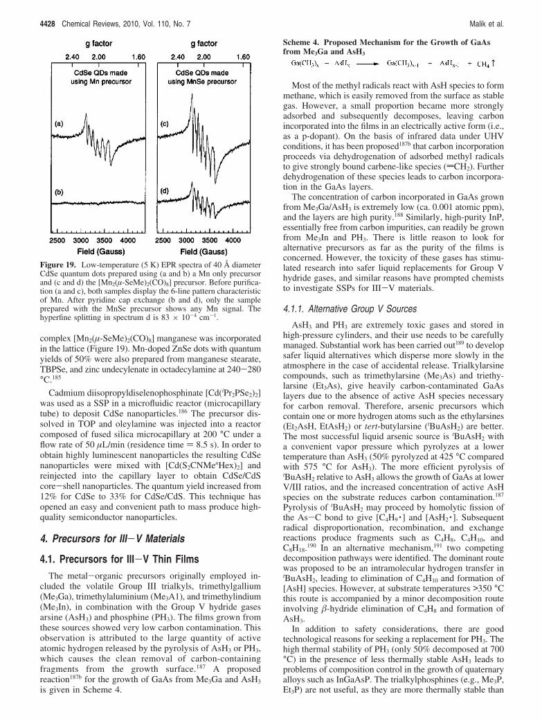
complex [Mn2(µ-SeMe)2(CO)8] manganese was incorporatedin the lattice (Figure 19). Mn-doped ZnSe dots with quantumyields of 50% were also prepared from manganese stearate,TBPSe, and zinc undecylenate in octadecylamine at 240-280°C.185
Cadmium diisopropyldiselenophosphinate [Cd(iPr2PSe2)2]was used as a SSP in a microfluidic reactor (microcapillarytube) to deposit CdSe nanoparticles.186 The precursor dis-solved in TOP and oleylamine was injected into a reactorcomposed of fused silica microcapillary at 200 °C under aflow rate of 50 µL/min (residence time ) 8.5 s). In order toobtain highly luminescent nanoparticles the resulting CdSenanoparticles were mixed with [Cd(S2CNMenHex)2] andreinjected into the capillary layer to obtain CdSe/CdScore-shell nanoparticles. The quantum yield increased from12% for CdSe to 33% for CdSe/CdS. This technique hasopened an easy and convenient path to mass produce high-quality semiconductor nanoparticles.
4. Precursors for III-V Materials
4.1. Precursors for III-V Thin FilmsThe metal-organic precursors originally employed in-
cluded the volatile Group III trialkyls, trimethylgallium(Me3Ga), trimethylaluminium (Me3A1), and trimethylindium(Me3In), in combination with the Group V hydride gasesarsine (AsH3) and phosphine (PH3). The films grown fromthese sources showed very low carbon contamination. Thisobservation is attributed to the large quantity of activeatomic hydrogen released by the pyrolysis of AsH3 or PH3,which causes the clean removal of carbon-containingfragments from the growth surface.187 A proposedreaction187b for the growth of GaAs from Me3Ga and AsH3
is given in Scheme 4.
Most of the methyl radicals react with AsH species to formmethane, which is easily removed from the surface as stablegas. However, a small proportion became more stronglyadsorbed and subsequently decomposes, leaving carbonincorporated into the films in an electrically active form (i.e.,as a p-dopant). On the basis of infrared data under UHVconditions, it has been proposed187b that carbon incorporationproceeds via dehydrogenation of adsorbed methyl radicalsto give strongly bound carbene-like species (dCH2). Furtherdehydrogenation of these species leads to carbon incorpora-tion in the GaAs layers.
The concentration of carbon incorporated in GaAs grownfrom Me3Ga/AsH3 is extremely low (ca. 0.001 atomic ppm),and the layers are high purity.188 Similarly, high-purity InP,essentially free from carbon impurities, can readily be grownfrom Me3In and PH3. There is little reason to look foralternative precursors as far as the purity of the films isconcerned. However, the toxicity of these gases has stimu-lated research into safer liquid replacements for Group Vhydride gases, and similar reasons have prompted chemiststo investigate SSPs for III-V materials.
4.1.1. Alternative Group V Sources
AsH3 and PH3 are extremely toxic gases and stored inhigh-pressure cylinders, and their use needs to be carefullymanaged. Substantial work has been carried out189 to developsafer liquid alternatives which disperse more slowly in theatmosphere in the case of accidental release. Trialkylarsinecompounds, such as trimethylarsine (Me3As) and triethy-larsine (Et3As), give heavily carbon-contaminated GaAslayers due to the absence of active AsH species necessaryfor carbon removal. Therefore, arsenic precursors whichcontain one or more hydrogen atoms such as the ethylarsines(Et2AsH, EtAsH2) or tert-butylarsine (tBuAsH2) are better.The most successful liquid arsenic source is tBuAsH2 witha convenient vapor pressure which pyrolyzes at a lowertemperature than AsH3 (50% pyrolyzed at 425 °C comparedwith 575 °C for AsH3). The more efficient pyrolysis oftBuAsH2 relative to AsH3 allows the growth of GaAs at lowerV/III ratios, and the increased concentration of active AsHspecies on the substrate reduces carbon contamination.187
Pyrolysis of tBuAsH2 may proceed by homolytic fission ofthe As-C bond to give [C4H9 · ] and [AsH2 · ]. Subsequentradical disproportionation, recombination, and exchangereactions produce fragments such as C4H8, C4H10, andC8H18.190 In an alternative mechanism,191 two competingdecomposition pathways were identified. The dominant routewas proposed to be an intramolecular hydrogen transfer intBuAsH2, leading to elimination of C4H10 and formation of[AsH] species. However, at substrate temperatures >350 °Cthis route is accompanied by a minor decomposition routeinvolving -hydride elimination of C4H8 and formation ofAsH3.
In addition to safety considerations, there are goodtechnological reasons for seeking a replacement for PH3. Thehigh thermal stability of PH3 (only 50% decomposed at 700°C) in the presence of less thermally stable AsH3 leads toproblems of composition control in the growth of quaternaryalloys such as InGaAsP. The trialkylphosphines (e.g., Me3P,Et3P) are not useful, as they are more thermally stable than
Figure 19. Low-temperature (5 K) EPR spectra of 40 Å diameterCdSe quantum dots prepared using (a and b) a Mn only precursorand (c and d) the [Mn2(µ-SeMe)2(CO)8] precursor. Before purifica-tion (a and c), both samples display the 6-line pattern characteristicof Mn. After pyridine cap exchange (b and d), only the sampleprepared with the MnSe precursor shows any Mn signal. Thehyperfine splitting in spectrum d is 83 × 10-4 cm-1.
Scheme 4. Proposed Mechanism for the Growth of GaAsfrom Me3Ga and AsH3
4428 Chemical Reviews, 2010, Vol. 110, No. 7 Malik et al.
PH3 and would in any case lead to increased carboncontamination.
The most successful alternative phosphorus source is, todate, tert-butylphosphine (tBuPH2),169 which is a liquid witha convenient vapor pressure (184.9 mbar at 10 °C) suitablefor a wide range of MOVPE applications. The intrinsictoxicity of tBuPH2 is lower than that of PH3 and pyrolyzesat a significantly lower temperature (50% pyrolyzed at 450°C), probably by homolytic phosphorus carbon bond fission.The reduced thermal stability of tBuPH2 relative to PH3
allows the growth of InP at lower V-III ratios and leads tosubstantial improvements in the uniformity of the InGaAsPdeposited. In addition to these advantages, tBuPH2 has morefavorable gas-phase chemistry than other RPH2 precursors,which can prereact with Me3In, even at room temperature,to liberate methane and deposit a white solid (probably an(MeInPR)n polymer). In contrast, tBuPH2 undergoes little orno homogeneous reaction, and this effect may be due to thelarge steric hindrance of the bulky tert-butyl group, inhibitingformation of gas-phase intermediates such as [Me3InPH2
tBu],likely precursors to the polymeric (MeInPR)n deposit.187
4.1.2. III-V Adducts
Several reviews have been published on the adduct-relatedcomplexes for III-V material deposition.192-194 Benz et al.used III-V adducts as substitutes for highly reactive groupIII trialkyls,195 and Moss and Evans used adducts asprecursors but synthesized them from the componentsdirectly in the reactor in order to avoid side reactions.196
Constant et al. proposed the use of Lewis acid-base adductsof general formula R2GaCl ·ER′3 (E ) As, P; R and R′ )Me, Et) to overcome the problem of the high reactivity andtoxicity of conventional dual sources.197 Films of GaP198,199
and InP199 have been grown from the corresponding[Et2M-PEt2]3 complexes (M ) Ga, In), two cyclic trimericmolecules with covalent metal-phosphorus bonds.200 Epi-taxial growth of GaAs has been achieved usingR2GaCl ·AsEt3 (R ) Me, Et).201 On the same kinds ofsubstrate, MOVPE of GaAs from (C6F5)Me2Ga ·AsEt3 and(Et2GaCl ·AsEt2)2CH2 was attempted. The former gaveepilayers on (111)-GaAs in the 600-700 °C temperaturerange, while with the latter epitaxial growth was observedon both types of substrate in the lower temperature range500-625 °C.202 These precursors belong to two series ofcompounds of general formula (C6F5)3-xMexGa ·AsEt3 (x )0 or 2) and (ClR2Ga ·AsEt2)2CH2 (R ) Me, Et),203 whosethermal decompositions have been systematically investi-gated by in-situ mass spectrometric analysis of the vapor ina cold-wall CVD reactor, with He and H2 as carriergases.204,205 In these studies, the role of the relative stabilitiesof the central M-E bond with respect to the peripheralM-ligand and E-ligand bonds was investigated through twodifferent approaches.192,206 The first approach involves theuse of rather fragile Lewis acid-base dative bonds, whosestrength can be tuned by means of the more or less electron-donating nature of alkyl groups and varied admixture ofhalogen (Cl) or pseudohalogen groups (C6F5). There areseveral drawbacks to this approach, such as loss in volatilityand surface mobility. The second approach uses complexeswith covalent M-E bonds as developed by Cowley andJones.207
4.1.3. III Nitrides
The precursors for metal nitride thin films need to be asnitrogen rich as possible in order to deliver as much activenitrogen to the surface as possible to engender stoichiometricgrowth. A number of alkylaluminum compounds including[Al(NR2)3]2, [HAl(NR2)2]2 (R ) Me, Et),208(Et2AlN3)3,209
(Me2AlNH2)3,210 and (Me2AlNiPr2)2211 have been used for
deposition of AlN films by CVD methods. NH3 has also beenused as a nitrogen source, but the high thermal stability ofammonia necessitates the use of high substrate temperature(>900 °C). This property leads to the loss of nitrogen in thedeposited AlN thin films. The films also retain a large amountof residual carbon, which has a direct consequence on thethermal conductivity and electrical resistivity of the films.212-214
In order to deposit stoichiometric AlN films, trimethylalumi-num–ammonia adduct, Me3AlNH3, has been used.215 How-ever, films are contaminated by carbon and oxygen. Incontrast to the trimeric amide (Me2AlNH2)3, the Me3AlNH3
species is monomeric and can be expected to have a highervolatility and more appropriate vapor pressure for MOCVDapplications. Pyrolysis studies have indicated that Me3AlNH3
decomposes with the evolution of methane to form alkyla-luminum amides or imides which contain a strong (Al-N)bond, and the following reaction sequence (Scheme 5) wasproposed.216
To deposit carbon-free AlN films at even lower temper-ature (200-250 °C), Al2(NMe2)6 has been used in CVDexperiments. Other types of compounds used for AlN filmsinclude hydrazidoalane dimers, [R2Al-µ-N(H)NMe2]2 (R )Me, Et).217 All of the above-mentioned compounds requirethe use of NH3 and Me3Al. A new type of air-stableprecursor, AlCl3:tBuNH2, a 1:1 adduct of aluminum trichlo-ride (AlCl3) and tert-butyl amine (tBuNH2), has been usedin MOCVD experiments.218 The resulting AlN films havenot only low carbon contamination but also a good N/Alatomic ratio. However, Cl contamination from AlCl3 isanother concern.
The decreasing bond strength of M-N in the series Al-N> Ga-N > In-N means the related gallium and, in particular,indium species are too unstable and dissociate in the hot zone,resulting in nonstoichiometric, poor-quality films. The amide[Ga(NMe2)3]2 only yielded GaN films in the presence ofammonia at substrate temperatures as low as 200 °C.219 Thefilms are amorphous, but this result indicates that theactivation energy of deposition may be lowered significantlywhen amide precursors are used. In particular, organometallicand inorganic azide compounds, e.g., [R2Ga(N3)]3 (R ) Me,Et),220,221 [(µ-NMe2)Ga(N3)(NMe2)]2,222 and [HClGaN3]4,223
have been shown to be useful precursors for nitride layers.The azide unit appears to be a very good choice to introducethe nitrogen component. A major drawback of azide deriva-tives is their potential for exothermic decomposition. Nitrogen-rich compounds such as (H2GaN3)224,225 and (N3)3Ga(R) (R) Me, Et)226 may even detonate under certain conditions.Hydrolysis of the M-N3 bond can take place to produceexplosive hydrazoic acid, which represents a major challengein view of the technical use of azide-type compounds. Inorder to overcome some of the technical difficulties, theintramolecularly Lewis base-stabilized compound[(N3)2Ga(CH2)3NMe2] has been synthesized.227 Transparent
Scheme 5. Proposed Mechanism for the Growth of AlNfrom Me3AlNH3
Main Group Elements in Semiconducting Materials Chemical Reviews, 2010, Vol. 110, No. 7 4429

GaN films have been grown from the compound in a cold-wall reactor with or without the use of ammonia. Filmsdeposited without using ammonia contained a smallamount of carbon, while the presence of ammoniaprevented the incorporation of carbon into the films. Inorder to obtain information on the decomposition pathwayof [(N3)2Ga(CH2)3NMe2], (Figure 20a) composition of thegas phase in the boundary layer above the substrate wasmonitored228 and species such as HGaN6, GaN6, HGaN2, andGaN2 were detected. The data gave clear evidence for theproduction of nitrogen-rich species in the boundary layer.
Kim et al. synthesized a Lewis acid-base adduct[Et2Ga(N3) ·MeHNNH2] of (H2GaN3) and deposited epitaxialh-GaN films on Si(111) substrate by MOCVD.229 It has beendemonstrated that the precursor undergoes protonation of theethyl ligands by methylhydrazine, and this occurs via lossof the stable N2, C2H6, and MeNNH, yielding good-qualityGaN films with little contamination. Other electron-donorligands such as hydrazine230 and methylamine231 have alsobeen employed to increase the volatility and stability ofcompounds followed by their subsequent use in MOCVDexperiments for GaN films (eqs 16 and 17).
Among the Group III nitrides, growth of InN is most difficultto achieve because of its low decomposition temperature,and hence, a low growth temperature is essential for InNfilms.232 Deposition of InN can be achieved at 300-400 °Cwith [(N3)In[(CH2)3NMe2]2 (Figure 20b).233 Due to theintermolecular Lewis base adduct stabilization, the compoundis not pyrophoric or explosive and even air stable (meltingpoint 340 K). At higher temperatures, the gas phase isdominated by In atoms. The In-N bond energy of indiumazides or indium amides as well as the dissociation energyof the diatomic species InN is significantly larger than forIn-C or weak donor-acceptor adducts. Therefore, conven-tional indium precursors preferentially produce indium atomsat the usual growth temperatures. Dimeric dimethylindiumazide, [Me2In(µ-N3)]2, prepared from reaction of Me3In withNH3 has been used in LP-MOCVD experiments to yieldhexagonal InN films on Si(111) substrates in the temperaturerange 350-450 °C.234
Boron nitride (BN) has also received considerable interestdue to its technological applications and excellent materialproperties: high hardness, chemical inertness, and dielectric
behavior. A number of physical and chemical techniqueshave been used to deposit cubic BN;235 however, thereremains a problem in controlling the boron and nitrogen ratio.To control the composition, Boo et al. synthesized a numberof compounds, namely, borane-triethylamine, tris(sec-butyl)borane,236 and isopropyl amine and tert-butylaminecomplexes of trietylborane. In the latter case, polycrystalline,crack-free hexagonal BN films have been deposited onSi(100) substrates at 850 °C, and importantly, films retainthe desired B:N ratio (1:1).237 A wide band gap (5.8 eV) isalso calculated from the optical transmittance data, andcarbon contamination in the films lowers the transmittance.The use of tris(dimethylamino)borane in the presence ofammonia and hydrogen gases has also been demonstratedin CVD to deposit hexagonal BN films and retain correctstoichiometry.238
4.1.4. III Phosphides and Arsenides
The chemistry involving a covalent M-E bond waspioneered by Beachly239,240 and extensively studied byCowley and Jones,241-243 Maury,244,245 and Wells.246-248 Thesecompounds were prepared to investigate their potential asprecursors for the CVD of III/V semiconducting materials.Many of the complexes prepared were used to grow thinfilms of materials such as GaAs.249 The structures for thesecomplexes are shown in Figure 21.
Cowley and Jones focused on the design and synthesis oforganometallics that feature σ-bonding between Group IIIand group V elements.207 Their work on GaAs was reviewedin 1994 as an illustration of the concept of a SSP.193 Theysuccessively tested three tetranuclear precursors:[Me2Ga(µ-AstBu2)]2,207,241,250-252 [Et2Ga(µ -AstBu2)]2,193 and[Ga(AstBu2)3].252 Both [Me2Ga(µ-AstBu2)]2 and [Et2Ga(µ-AstBu2)]2 have a (M2E2) ring in their solid-state structures.
Preparation of these dimeric precursors243 involved reactionof di-tert-butylarsine and trimethylgallium or triethylindium.This method involves preparation of Grignard, its reactionwith arsenic trichloride to obtain tBu2AsCl, which is thenhydrogenated by LiAlH4 to give di-tert-butylarsine.253 Aslightly modified method was reported by O’Brien et al.,254,255
where instead of reacting trimethylgallium and di-tert-butylarsine at 57 °C for 4 days as reported by Cowley etal.243 the reactants were dissolved in diethyl ether and
Figure 20. Molecular structures of (a) [(N3)2Ga(CH2)3NMe2] and(b) (N3)In[(CH2)3NMe2]2.
Et3Ga + MeHNNH2 · HCl98Et2O
0 °CEt2GaCl · MeHNNH2 +
C2H6 (16)
Et3GaCl · MeHNNH2 · HCl + NaN398THF
Et2GaN3 · MeHNNH2 + NaCl (17)
Figure 21. Structure of single-source precursors for III-Vmaterials.
4430 Chemical Reviews, 2010, Vol. 110, No. 7 Malik et al.

refluxed at 40 °C for 3 days. X-ray single-crystal structuresof [tBu2AsGaMe2]2
254 and [tBu2AsInEt2]2255 are shown in
Figure 22.[Me2Ga(µ-AstBu2)]2 was used to deposit GaAs thin films
by LP-CVD at a precursor delivery temperature of 145 °Cand deposition temperature of 450-700 °C using H2 or Heas the carrier gas. The films deposited were arsenic defi-cient.250 Substitution of ethyl groups for methyl is known tolower carbon contamination. Epitaxial films were obtainedfrom [Et2Ga(µ-AstBu2)]2 over the temperature range 400-500°C but showed low Hall mobilities due to the presence ofGa islands caused by highly reactive ethylgallium species.193
The use of Ga(AstBu2)3, which contains an excess of arsenicand no gallium-carbon bonds, produced films with carbonlevels about two orders of magnitude lower than from themethyl derivative ([Me2Ga(µ-AstBu2)]2). The excess ofarsenic in the precursors gave rise to n-type films, while theywere p-type with [Me2Ga(µ-AstBu2)]2 or [Et2Ga(µ-Ast-
Bu2)]2).252 Pyrolysis251,256 and temperature-programmed de-sorption252 studies suggest two modes of decomposition forthese precursors: As-C bond hydrogenesis to form tBuradicals and -H elimination from tBuAs moieties followedby CH3 · · ·H coupling at Ga to form isobutene and methane.
Trimeric hexanuclear complexes such as [Me2Ga(µ-AsMe2)]3 and [Me2Ga(µ-AsiPr2)]3 failed to give GaAs filmsbecause of the facile loss of tetraalkyldiarsine, as shown bypyrolysis studies.256,257 [nBu2Ga(µ-AstBu2)]2 has been usedto grow epitaxial GaAs either by ultrahigh vacuumMOCVD258 or by spray pyrolysis.259 Films of InP have beenprepared by Cowley et al.207,241 and Bradley and co-workers,260 independently, from the same tetranuclear mol-ecule, [Me2In-PtBu2]2. Cowley et al.207,241 carried out thedeposition studies at temperatures between 450 and 700 °Cin a cold-wall reactor with H2 or He as the carrier gas.Bradley et al.260 used an MBE reactor and found thatstoichiometric growth was only possible at 480 °C with asimultaneous flux of dissociated phosphine. Indium-rich filmswere obtained at lower temperature.
4.1.5. III Antimonides
Cowley et al. deposited GaSb and InSb films on Si(100)wafers at 450 °C from six-membered heterocycles of the type[Me2MSbtBu2]3 (M ) Ga, In) in a horizontal hot-wallMOCVD reactor under high-vacuum conditions (10-3
mbar).261 AlSb films on Si(100) and polycrystalline Al2O3
substrates have been reported in a cold-wall MOCVD reactorbetween 300 and 550 °C using [Et2AlSb(SiMe3)2]2 or[iBu2AlSb(SiMe3)2]2.262 A large amount of Si contaminationhas been observed, which is likely to originate from afragmentation reaction of the SiMe3. Schulz and his groupreported alkyl-substituted heterocycles of the type[R2MSbR′2]x (M ) Ga, In; x ) 2, 3) by a novel reactionpathway termed a distibine cleavage reaction. DistibinesSb2R4 (R ) Me, Et, iPr, nPr) were found to react withtrialkylgallanes and indanes MR′3 (M ) Ga, In) withformation of the corresponding Lewis acid-base adduct[R′3M]x[Sb2R4], which then consequently undergoes a Sb-Sbbond cleavage reaction with formation of the four- or six-membered heterocycle [R2MSbR′2]x.263-265 Crystalline GaSbfilms were deposited from [tBuGaSbEt2] in a cold-wallMOCVD reactor without the need for any carrier gas, andthe best results were obtained at substrate temperaturesbetween 400 and 500 °C (Figure 23).266
4.2. Precursors for III-V NanoparticlesColloidal methods have been used for the preparation of
AlN, GaN, and InN nanoparticles. GaN nanocrystals have beenprepared by thermal decomposition of compounds includingpolymeric gallium imide, Ga(NH)3/2n, and gallium azides,[Et2GaN3]3, (N3)2Ga[(CH2)3NMe2], or (Et3N)Ga(N3)3.267-269
The amount of azide precursors used affects the size of the
Figure 22. Structures of [tBu2AsGaMe2]2.
Figure 23. SEM images displaying the surface morphology ofGaSb films grown from [tBu2GaSbEt2]2 at 400 (a and b), 450 (cand d), 500 (e and f), and 550 °C (g and h).
Main Group Elements in Semiconducting Materials Chemical Reviews, 2010, Vol. 110, No. 7 4431

particles, which are usually 20-200 nm agglomerates withnanocrystalline domains of ∼4 nm. The use of poly(imi-dogallane) precursor for production of GaN requires difficultand hazardous manipulation of pure ammonia.267 Thecomplex has poor solubility, which is detrimental to particlesize control. At high temperature in coordinating solvent onlya small percentage of nanosized material is obtained.Pyrolysis of this compound gave GaN.270 The new methodnot only significantly improved the yield of colloidal GaNnanocrystals but also eliminated the need for ammonia. Thiseffect is probably due to the good solubility of the dimericcompound and the ability of the coordinating ligands to capthe particle surfaces as soon as GaN nuclei are formed. Thepyrolysis reaction appears to involve transamination byhexadecylamine (HDA). In the absence of HDA in thereaction mixture, no GaN is produced.270 Adducts of metalchlorides and urea such as [M(H2NCONH2)6]Cl3 (M ) Al,Ga) and In(H2NCONH2)3Cl3 have been used to form wurtzic(hexagonal) nanocrystals of AlN, GaN, and InN by refluxingthe precursors in n-trioctylamine.271 GaN nanocrystals with2-3 nm in diameter exhibited two emissions bands centeredat ca. 380 and 340 nm. In the case of indium precursor, asmall proportion of indium oxide is also grown. Similar to(N3)2Ga[(CH2)3NMe2], the indium analogue decomposes inTOPO to yield cubic InN nanoparticles in the 2-10 nm sizerange (Figure 24).272 Fractionated particles with an averagediameter of 4.5 nm exhibited luminescence at 690 nm (1.82eV), consistent with the band gap of the bulk material beingnear 0.7 eV. These are the first InN particles in which nearband-gap emission was observed.
Solvothermal synthesis of wurtzite InN nanocrystals fromInBr3 and NaN3 is reported in superheated toluene andrefluxing in hexadecane at 280 °C.273 InN from hexadecaneand lower temperature toluene reactions produced lesscrystalline nanoparticles with a zinc blende (cubic) compo-nent. Mixed indium and gallium azide precursors in tolueneproduced mixed metal nitrides, Ga1-xInxN, where x is 0.5and 0.75. Both InN and Ga-In-N systems showed red- andgreen-filtered visible fluorescence emission. A mixture ofcubic and hexagonal (InGa)N particles has also been reportedby ammonolysis of the precursor ammonium hexafluoroin-dategallate [(NH4)3In1-xGaxF6].274 The ratio of cubic tohexagonal material is ∼9:1. The material exhibited photo-
luminescence in the visible region around 735 nm (1.69 eV)at room temperature.
InP and GaP nanocrystals were synthesized from diorga-nophosphides [M(PtBu2)3] (M ) Ga, In).275,276 Thermolysisin dry alkylpyridine results in formation of capped nano-particles which exhibited distinct optical quantum size effects.The decomposition mechanism of precursors involved acomplicated mix of reductive and -hydrogen elimination,resulting in metal phosphide and metallic impurities. Wellset al. reported GaP nanoparticulates by thermolysis of[X2GaP(SiMe3)2]2 (X ) Br, I) or (Cl3Ga2P)n, both de-composing at relatively low temperatures under vacuumto yield crystalline monodispersed GaP.277 Thermolysis of[H2GaE(SiMe3)2]3 (E ) P, As) at 450 °C in xylene also gavenanoparticles of GaP or GaAs approximately 5 nm indiameter.278 HDA-capped InAs and GaAs nanoparticles canbe efficiently synthesized from dimeric compounds[tBu2AsInEt2]2 and [tBu2AsGaMe2]2, respectively.279,280 Inboth cases, nanoparticles show a considerable blue shift intheir optical spectra as compared to parent bulk materials.
5. Precursors for III-VI Materials
5.1. Precursors for III-VI Thin FilmsThe Group III and VI elements form compounds with
several stoichiometries and in a number of phases: M2E3 (M) Ga, In; E ) S, Se, Te), a zinc-blende type (M ) Ga) anda defect spinel (M ) In) and ME (with the same layeredstructure as in M2E3).281 The III-VI materials are alternativesto those in the II-VI series, especially in photovoltaicapplications. However, their polytypism and the variety ofstoichiometries accessible are a problem as compared to theII-VI materials, and the availability of some of the elements,notably indium, is somewhat limited.
5.1.1. Thiolato Complexes
Preparation of III-VI thin films started with the use of asingle-source system282,283 unlike the II-VI or III-V materi-als for which growth of the films was initially carried outusing two sources. Indium and gallium thiolato complexesare typically involatile polymeric aggregates similar to thoseformed by Group 12 thiolates.284 Nomura et al. successfullyprepared dimeric volatile alkylindium alkyl thiolates byintroducing steric bulk at both the alkyl and the thiolate.285
These compounds are typically liquids at room temperatureand can be distilled under reduced pressure (>10-3 Torr).Deposition of the two different types of indium sulfide wascontrolled by the number of thiolate ligands bound to theindium atom; dialkylindium monothiolates give InS, andmonoalkylindium dithiolates produce -In2S3 at 300 °C understatic pyrolysis conditions. Nomura’s group used nBu2In(SiPr)as a source for indium sulfide deposition, and highlyorientated films of -In2S3 with a strongly preferred (103)growth direction were deposited on Si(111) or quartzsubstrates at temperatures in the range 300-400 °C.286
Orthorhombic InS films could be deposited at lower tem-peratures using Bu2In(SPr) as a source, but the presence oftrace amounts of oxygen in the carrier gas caused partialoxidation of the InS layers, leading to highly conductive filmsof indium oxide doped with sulfur at 275 °C.287
Barron and co-workers deposited a novel metastable cubicGaS phase from the [tBuGaS]4 cube at temperatures in theregion of 400 °C; in this case it is tempting to draw a
Figure 24. HR-TEM image of InN nanoparticles. The principalzone axes of the cubic unit cell are indicated for the top particle.(Inset) Fourier transform electron diffraction pattern of the particlein the top of the image.
4432 Chemical Reviews, 2010, Vol. 110, No. 7 Malik et al.

correlation between the cubic phase observed and the cubanestructure of the precursor as shown in Figure 25.288,289
Another interpretation of this observation is that the filmsdeposited are extremely sulfur deficient as deposition alsoled to an amorphous gallium containing ca. 20% sulfur andthat the phase deposited is driven by the ratio of pnictide tometal delivered to the substrate.
In related work the dimeric indium thiolate [tBuIn(µ-StBu)]2was used to deposit a polycrystalline, tetragonal high-pressure form of -In2S3.288,289 The authors believe that thecubic GaS films might be useful as a passivation layer onGaAs wafers. The gallium sulfide cubane can be preparedby reaction of GatBu3 with H2S followed by static pyrolysisat 45 °C.289 Gysling et al. deposited thin films of a novelcubic InSe (300-250 °C) and the known hexagonal In2Se3
(470-530 °C) on GaAs(100) by a modified MOCVD methodusing a sonicated spray evaporator from Me2InSePh andIn(SePh)3 as precursors. The structures of the precursors areunknown, and the spray MOCVD process was developed todeal with the relatively low volatility of the precursors.290
5.1.2. Thiocarbamato Complexes
Films of indium sulfide have been grown from dimethyl-,diethyl-, or dineopentyl-indium diethyldithiocarbamates([R2InS2CNEt2] with R ) Me, Et, or Np), which are air-sensitive compounds.291,292 The films were grown on (100)-GaAs substrates using a cold-wall, low-pressure reactor. Themethyl complex deposits orthorhombic InS and monoclinicIn6S7 phases between 425 and 400 °C, whereas growth at325 °C results in cubic -In2S3. In contrast, the ethylcompound deposits monophasic, crystalline -In2S3 over therange 350-400 °C. These results show the role played bythe change of alkyl groups. They suggest that the amount ofcarbon incorporation, which relates to the -H eliminationprocess, may well influence the film’s composition. Experi-ments with related gallium precursors were less conclusive.
Tris complexes of indium [In(E2CNMeR)3] have been usedin experiments where E ) S with R ) nbutyl or nhexyl andE ) Se with R ) nhexyl.292 In2S3 films were grown from[In(S2CNMenBu]3] or [In(S2CNMenHex)3] at 450-500 °Conto glass, GaAs, or InP by LP-MOCVD.293 Cubic R-In2Se3
was the predominant phase, sometimes mixed with somehexagonal -In2Se3 phase when the n-butyl derivative wasused. Deposition of predominately R-In2Se3 regardless ofgrowth conditions shows a clean gas-phase decompositionprocess. In2S3 nanorods with an average diameter of 20 nmand 400-500 nm length were prepared for the first time onglass substrates from a single-source precursor,[Et2InS2CNMenBu], by AACVD at 375 °C without eithertemplate or catalyst.294
5.1.3. Xanthato and Monothiocarbamato Complexes
[In(S2COiPr)3] is a volatile complex from which thin filmsof cubic R-In2S3 could be grown at temperatures as low as
210 °C. Films deposited on glass were (111)-orientated.295
These results are interesting with regard to the depositionof the related ternary CuInS2 and CuInSe2 using complexesof the type [M[E2CNMeR]n], where R ) nBu and nHex, M) Cu (n ) 2) and In (n ) 3).296 Thin films of In2S3 havebeen produced from [In(SOCNEt2)3]297 and [In(SOCNi-
Pr2)3]298 on glass substrates by LP-MOCVD. [In(SOCNiPr2)3]proved to be both more volatile and more efficient for filmdelivery than [In(SOCNEt2)3]. The former led to the tet-ragonal -phase at temperatures as low as 350 °C and thelatter to the cubic -phase at 400 °C and above (Figure 26).Hampden-Smith and co-workers used the facile eliminationof thioacetic anhydride from polyether adducts of group 2metal thioacetates to deposit high-purity, stoichiometric metalsulfides299 and applied it to adducts of gallium and indiumthioacetates.300 Two gallium complexes, MeGa(SCOMe)2-(dmp) and Ga(SCOMe)3(dmp) (dmp ) 3,5-dimethylpyri-dine), and an indium complex, [Hdmp]+[In(SCOCH3)4]- 301
have been used by the AACVD method to prepare thin filmsof the metal sesquisulfides. The respective proposed decom-position pathways for the gallium and indium complexes areshown in eqs 18-20.
5.1.4. Dichalcogenoimidodiphosphinato Complexes
The compounds [M(µ-Te)N(iPr2PTe)2]3 (M ) In, Ga) havebeen employed to deposit M2E3 films onto glass and Si(100)substrates at deposition temperatures between 325 and 475°C.302 The indium precursor gave cubic In2Te3 exclusively,whereas the gallium complex generated a mixture of cubicGa2Te3, monoclinic GaTe, and hexagonal Te. Mass spec-trometric studies indicate that fragmentation of the indiumprecursor to give In2Te3 is accompanied by formation of[In[N(iPr2PTe)2]2]+ and [N(iPr2PTe)2]-2. These complexes are
Figure 25. Cubic structure of [tBuGaS]4.
Figure 26. SEM images of -In2S3 films deposited from [In(SOC-NiPr2)3] at (a) 300, (b) 350, (c) 400, and (d) 450 °C on glasssubstrates (note, amorphous at 300 °C).
2Ga(SCOMe)2(CH3)(dmp) f 2dmpy +[MeC(O)SC(O)Me] + 2(Me2CO) + Ga2S3 (18)
2Ga(SCOMe)2(dmp) f 2dmpy +3[MeC(O)SC(O)Me] + Ga2S3 (19)
2(Hdmp)+[In(SCOMe)4] f 2HSOCMe +2(dmp)In(SOMe)3 f 2(dmpy) +
3[MeC(O)SC(O)Me] + Ga2S3 (20)
Main Group Elements in Semiconducting Materials Chemical Reviews, 2010, Vol. 110, No. 7 4433

structurally different from the earlier homoleptic Cd precur-sors of the [N(iPr2PTe)2]2, which contain a central preformedM3Te3 (M ) In, Ga) ring, with each tetrahedral metal centerfurther coordinated by a [N(iPr2PTe)2]2 ligand (Figure 27).303
The general method of synthesis is shown in Scheme 6.The TGA of these complexes showed them to decompose
in a single step between 300 and 375 °C for indium complexand 280 and 360 °C for gallium complex. Both precursorsafford a significantly large residue (59% for indium complex,58% for gallium complex), indicating incomplete decom-position or the presence of impurities after decompositionof precursor. The structures of most common ligands usedfor the preparation of different metal complexes are givenFigure 28.
5.2. Precursors for III-VI NanoparticlesDimitirjevic and Kamat prepared colloids of In2Se3
stabilized with either poly(vinyl alcohol) (PVA) or sodiummetaphosphate (SMP).304 They reported particles with di-ameters of approximately 2-3 (SMP stabilized) and 30 nm(PVA stabilized) with absorption maxima at 375 and 250nm (SMP stabilized) and an onset of absorption at ap-proximately 550 nm (PVA stabilized). The same authorsreported the synthesis of In2S3 colloids in acetonitrile, withparticle diameters ranging between 100 and 200 nm.305
Barron et al.306 reported the preparation of nanoparticles ofGaSe and InSe by MOCVD using the cubane precursors[(tBu)GaSe]4 and [(EtMe2C)InSe]4. The GaSe particles hada mean diameter of 42 nm with a standard deviation of 13nm, whereas the spherical InSe particles were 88 nm in
diameter with a standard deviation of 30 nm. The particlesize was determined by TEM, and no optical data wasreported. O’Brien et al.307 reported the synthesis of InS andInSe nanoparticles capped with TOPO and nanoparticles ofInSe capped with 4-ethylpyridine (Figure 29) from[In(E2CNEt2)3] (E ) S, Se).
GaSe nanoparticles (2-6 nm) were prepared from Me3Gaand TOPSe in a high-boiling solution of TOP and TOPO.308
GaSe has a hexagonal layered structure309 consisting ofSe-Ga-Ga-Se sheets which are only weakly attracted byvan der Waals interactions. GaSe can be either , γ, or εphase depending upon the arrangement of layers. GaSenanoparticles (88 nm) were also synthesized from (RGaSe)4
cubanes by the MOCVD method.310 TEM images showednanowire-type structures.
Dutta et al. reported the preparation of In2S3 nanopar-ticles from SSPs such as indium xanthates.311 The sameauthors previously used methylindium thiolate complexesbut produced indium sulfide nanoparticles of poor qua-lity.312 Recently, they used polymeric indium and galliumprecursors synthesized by reaction of trimethyl gallium/indium ether adduct (Me3Ga/InOEt2) with 1,2-ethanedithiol(HSCH2CH2SH) in 1:1 stoichiometry. Ga2S3 and In2S3
nanoparticles were prepared by pyrolysis of these precursors[MeM(SCH2CH2S)]n (M ) In, Ga) in a tube furnace between300 and 500 °C.313
6. Precursors for IV-VI Materials
6.1. Precursors for IV-VI Thin FilmsTin and lead chalcogenates are narrow band-gap semi-
conductor materials and have attracted considerable inter-est recently due to their many potential applications. CubicPbS has been deposited from several lead dithiocarba-mato complexes. PbS films have been deposited from[Pb(S2CNEt2)2] in the temperature range 425-500 °C witha source temperature of 210 °C and in the temperature range230-300 °C by remote plasma-enhanced MOCVD.314 Dueto its volatility, [Pb(S2CNnBu2)2] was used from among
Figure 27. Molecular structures of Cd[(SePiPr2)2N]2,Sb[(TePiPr2)2N]3, and [M(µ-Te)[N(iPr2PTe)2]3 (M ) In, Ga).
Scheme 6. General Synthesis of Tellurium DerivativesFigure 28. Some common ligands used for metal complexation.
4434 Chemical Reviews, 2010, Vol. 110, No. 7 Malik et al.

several dithiocarbamato complexes to deposit PbS films ontoglass and Si(100) in the temperature range 400-600 °C.315
Asymmetric derivatives of lead dithiocarbamates[Pb(S2CNRR′)2] (R ) Me, Et; R′ ) iPr, nBu) also proved tobe useful in LP-MOCVD and AACVD experiments todeposit cubic PbS films.316 A degree of control over themorphology of the deposited material can be exerted by ajudicious choice of growth technique, precursor, and substrate/precursor temperatures. Dichalcogenoimidodiphosphinatocomplexes (Scheme 7) of [Pb[(EPiPr2)2N]2] (E ) S, Se, Te)proved to be useful SSPs for lead chalcogenide thin films(Figure 30).316,317 All compounds are air stable except[Pb[(TePiPr2)2N]2], which is highly unstable. Depositionexperiments conducted at 475 °C produced pure PbTe films.Deposition at lower growth temperatures lead to formationof both PbTe and Te phases.
Deposition of PbSe thin films from diselenophosphinatoand imidodiselenodiphosphinato lead complexes316 alwaysresults in significant contamination with phosphorus. In orderto overcome this problem, we synthesized (4-nitro-N,N-diisobutyl-N-benzoylselenoureato)Pb(II) and N,N-diethyl-N-benzoylselenoureato)Pb(II) complexes to be used as SSPsfor deposition of PbSe thin films.318
Dahmen and co-workers tested bis[bis(trimethylsilyl)m-ethyl]tin chalcogenides, [SnCH(SiMe3)22(µ-E)]2 (E ) Se,Te), for the MOCVD of SnSe and SnTe thin films.319,320 Theyare dimers in solution as well as in the solid state. Thecompounds are air stable and volatile.321 MOCVD experi-
ments indicated that both compounds show strong selectivityin the decomposition reaction toward the metallic substrates,thus demonstrating the need for a seeding metallic layer toinitiate growth. In the case of nonmetallic substrates, no filmdeposition was obtained under all experimental conditions.
A number of metal alkoxide precursors have been synthesizedand utilized for deposition by CVD production of SnOx thinfilms: [Sn(OCH(CF3)2)4(HNMe2)2]322 and Sn(OCMe3)4.323324
The fluorinated species yield halide-doped films, which areof interest in high-conductivity applications but may beproblematic for other applications. The OCMe3 speciesproved to be useful for production of SnO2 films withoutthe use of an oxidant. Boyle et al. prepared a family of oxo-alkoxyl precursors which include [Sn(µ-ONep)2]∞ (ONep )OCH2CMe3) and its hydrolysis products [Sn5(µ3-O)2(µ-ONep)6] and [Sn6(µ-O)4(µ-ONep)4] for MOCVD applica-tions.325,326 All compounds possess relatively low meltingpoints (>190 °C) and volatility for direct vaporization. Atlow temperatures the oxides are favored, but at highertemperature metallic tin spheres are generated. The in-situ-generated metal droplets act as a catalyst for the growth ofSnO2 wires and ribbons as opposed to uniform thin films.
Tin oxide (SnO2) films composed of different grain sizesand morphologies particles are obtained by the CVD of[Sn(OtBu)4] in the temperature range 500-700 °C.327 Thesensitivity of SnO2 surfaces toward CO gas significantlydepends on the microstructure and specific surface area. Thebetter sensing performance of films deposited at highertemperature (700 °C) is due to the porous structure whichincreases the amount of oxygen-dangling bonds in themicrostructure and overall specific surface area responsiblefor the improved gas sensitivity.328 A new volatile precursor[SnCl4OC(H)OC2H52] provides high growth rates (up to100 Å s-1 at 560 °C) in APCVD reactor.329 Fluorine-dopedtin oxide (SnO2:F) films were deposited from 2,2,2,-trifluo-roethyl trifluoroacetate as a fluoride source. Resistivities aslow as 5.9 × 10⁻⁴ Ω cm and mobilities as high as 27.3 cm2
Figure 29. 4-Ethylpyridine-capped InSe nanoparticles from [In(Se2CNEt2)3]: (a) TEM micrograph and (b) size distribution histogram.
Scheme 7. Synthetic Scheme for Pb[(TePiPr2)2N]2
Figure 30. SEM micrographs of PbSe deposited from Pb[(SePiPr2)2N]2 by LP-MOCVD at (Tprec/Tsubs) (a) 250/425 and (b) 250/450 °C.
Main Group Elements in Semiconducting Materials Chemical Reviews, 2010, Vol. 110, No. 7 4435

V-1 s-1 are routinely observed. No significant variation ingrowth rate and film thickness is observed for the SnO2
compared to the SnO2:F films. Molloy and co-workersdeveloped several organotin fluorocarboxylate compoundsfor APCVD of fluorine-doped SnO2 films.330 Et3SnO2CC2F5,
in particular, gives high-quality films with fast depositionrates despite adopting a polymeric, carboxylate-bridgedstructure. Films grown from Me2Sn(O2CCF3)2 contained highlevels of fluorine dopant but exhibited diminished physicalproperties. The gas-phase structure of Me3SnO2CC2F5 indi-cated that accessible conformations do not allow contactbetween tin and fluorine, and therefore, direct transfer isunlikely to be part of the mechanism for fluorine incorpora-tion into SnO2 films. A mechanism that involved the loss ofCO2 to generate R3SnR′ in situ is much likely.
Deposition of tin sulfide (SnS) films from precursors suchas [Sn(SCH2CF3)4] or [Sn(SPh)4] requires hydrogen sulfide(H2S) as an additional sulfur source.331,332 These precursorson their own do not result in SnS. This was attributed tofacile disulfide (RS-SR) elimination, which is due to thepresence of noncovalently bonded S · · ·S interactions and cis-annular interactions in the molecules like [M(SR)4], whereM is a Group IV element.333 Thermogravimetric analysis andmass spectrometry data showed that [Sn(SR)4] results inRS-SR in the gas phase, supporting formation of disulfideduring the CVD process.333 However, in the presence ofminimal flow of H2S it was possible to deposit SnS films. Itis predicted that the sulfur in tin sulfide may be from H2Sgas and not from the thiolate precursors.334 Even unsym-metric tin dithiocarbamates334 and tin complexes containingchelating ligands333 possessing a direct Sn-S bond may ormay not form SnS in the absence of H2S gas. It wasestablished that chelating thiolate ligands could hinderdisulfide elimination.333 Thus, Parkin et al. reported the useof chelating dithiolato ligand complex [Sn(SCH2CH2S)2] fortin sulfide coatings on glass using AACVD.333 Recently, wehave shown simple tin thiosemicarbazone complexes for theSnS films on glass by AACVD.335 In such compounds,disulfide elimination is hindered due to the absence of anyRS ligand and also the absence of more than one S-containing ligand of any sort. Both molecules contain only
Figure 31. SEM images of SnS2 (top) and SnS (bottom) depositedfrom [SnCl4o-C6H4(CH2SMe)2] at 650 °C.
Figure 32. (a and b) Dark field TEM images of ultranarrow PbS rods. (c) HRTEM image of ultranarrow PbS rods showing a diameter of1.7 nm with well-resolved lattice planes. (Inset) HRTEM showing the interplanar distances of the lattice planes; the arrow indicates thegrowth direction. (d) SAED pattern from the ultranarrow rods.
4436 Chemical Reviews, 2010, Vol. 110, No. 7 Malik et al.

one thio ligand, and hence no S · · ·S interaction is possible,i.e., disulfide elimination is not feasible and SnS films aredeposited without H2S gas. New complexes derived fromSnCl4 with the o-xylyl dichalcogenoethers o-C6H4(CH2EMe)2
(E ) S, Se) and Et2Se have been reported.336 LPCVD ofcomplex [SnCl4o-C6H4(CH2SMe)2] leads to depositionof hexagonal SnS2 at lower temperature and orthorhombicSnS at high temperatures (Figure 31), while [SnCl4o-C6H4(CH2SeMe)2] deposits poor-quality SnSe2 films at 600°C. The Et2Se derivative [SnCl4(Et2Se)2] leads to uniformdeposition of SnSe2 with growth perpendicular to thesubstrate.336 Depositions of SnS and SnS2 are rare examplesof metal sulfide deposition from C-S bond fission within athioether complex.
Reports on the deposition of germanium chacogenides areextremely rare. Only recently, germanium telluride thin filmswere reported from a single-source route.337 Insertion reactionbetween a germylene and dialkyl telluride leads to a stablealkyl tellurolato compound which has been used to depositGeTe films in MOCVD studies.
6.2. Precursors for IV-VI NanoparticlesOne of the earliest reports of the deposition of PbS
involved the use of the diethyldithiocarbamate to producewell-defined cubes.338,339 It was subsequently shown thatshape control was possible with changes in the reactionconditions.340 Many precursors have been used to depositPbS or PbSe.338-345 Decomposition of lead hexadecylxanthatein trioctylamine has been reported to yield ultranarrow rodswith a diameter of ∼1.7 nm and lengths of 12-15 nm (Figure32).345 Strong quantum confinement is observed in theabsorption and photoluminescence spectra. The absorptionband is strongly blue shifted and has a sharp excitonic bandat 278 nm and a shoulder at 365 nm.
These bands are of excitonic origin corresponding to the1Pe to 1Ph, 1Se to 1Ph, and 1Se to 1Sh transitions.346-348
The PL spectra show strong and sharp band-edge emissionat 410 and 434 nm along with a shoulder at 465 nm and aweak band at 500 nm. Recently, Alivisatos and co-workersreported the conversion of Cu2S rods to PbS simply bycation-exchange reactions.349 This reaction proved to be muchmore favorable than converting CdS rods to PbS. This effectis possibly due to fact that the soft base, tri-n-butylphosphine,binds strongly to the Cu+ cation as compared to Cd2+ orPb2+ and provides more control.
Vittal et al. synthesized PbS particles by employing aLewis-base-catalyzed approach to decompose metal alkylxanthates by using alkyl amines as a solvent to promotedecomposition as well as capping ligand for the particlesformed.343 Spherical PbS nanoparticles of diameter 5-10 nmwere obtained when long-chain alkylamines were used. Whenethylenediamine was used instead, PbS dendrites wereisolated from the same precursor at room temperature.Uniform six- and four-armed dendrites were observed, withregular branches of ∼20 nm in diameter growing in a parallelorder. These kinds of precursors were stable for periods ofmonths, easy to synthesize, and decomposed with high yields.Cheon and co-workers provided some insight into factorsunderlying the ripening observed with the PbS nanoparticlesfrom a single-source precursor.342 By varying the ratioinjection temperature, the shape of the resulting particlesevolved from rods to multipods to cubes.
Single-source precursors have been used by a hydrothermalprocess to grow a range of PbS nanocrystals.350 More
recently, Bi nanoparticles have been used to catalyzesolution-liquid-soild (SLS) growth of PbS nanowires from[Pb(S2CNEt2)2] (Figure 33).351 The minimum controllednanowire diameters that can be typically achieved from Bicatalysts is ca. 5 nm, because the small Bi nanoparticles (d< 5 nm) required to produce smaller nanowire diameters arevery unstable with respect to agglomeration.
The use of tin dithiocarbamate [Sn(S2CNEt2)2] in oley-lamine has been reported to yield SnS nanocrystals, andreaction conditions do not require the use of hazardousmaterials such as the use of phosphines and volatile orga-nometallic compounds.352 The crystalline SnS nanocrystalsdisplay strong optical absorption in the visible and NIRspectral regions.
7. Precursors for V-VI Materials
7.1. Precursors for V-VI Thin FilmsOnly a handful of reports exist concerning the deposition
of Group V-VI thin films using a single molecular precursorapproach. Thin films of antimony oxide have been depositedby atmospheric-pressure (AP) MOCVD in the temperaturerange 400-600 °C using the antimony alkoxides tris(n-
Figure 33. Representative TEM images of PbS nanowires ofvarious diameters (d): d ) (a) 8.7 ( 2.4 ((28%), (b) 11.2 ( 2.3((21%), (c) 16.1 ( 2.9 ((18%), and (d) 31.2 ( 3.9 nm ((13%).(e) Lattice-resolved HRTEM image of a 15 nm diameter PbSnanowire. (Inset) Indexed fast-Fourier-transform (FFT) pattern ofthe image, indicating that the nanowire grows along the 200direction.
Main Group Elements in Semiconducting Materials Chemical Reviews, 2010, Vol. 110, No. 7 4437

butoxyantimony) with [Sb(OnBu)3] and trisethoxyantimony[Sb(OEt)3] as precursors.353,354 Both precursors have beenused to deposit the senarmontite form of Sb2O3 with apreferred orientation along the (111) direction, and additionof oxygen gas to the precursor stream leads to formation ofthe mixed valence oxide, Sb6O13. Subsequent work has madeuse of tris(N,N-dimethylcarbamato)antimony [Sb(O2CNMe2)3] inLP-MOCVD to deposit the senarmonite form of Sb2O3.355 Inanother article, the same group described the influence ofcarefully controlled process parameters on the deposition of
SbOx.356 A range of antimony(III) and antimony(III/V) oxidescan be produced from the precursors antimony(III) ethoxide,butoxide, neopentoxide, and carbamate. At low temperatures,single-phase senarmontite is produced in a hot-wall reactorat atmospheric pressure, and variation of growth parameters,such as growth temperature and choice of precursor, allowscontrol of the films microstructure and texture. Depositionin a cold wall under low pressure leads to formation ofgranular rather than continuous senarmontite films. Additionof oxygen to the precursor or use of the carbamate precursorallows formation of the higher oxidation state phase.
A series of unsymmetrical antimony dithiocarbamates[Sb(S2CNMeR)3] (R ) nBu, nHex, Bz) has been used inAACVD to deposit Sb2S3 films; the film purity was depend-ent on substrate temperature.357 Despite their relatively lowmelting points, none of the compounds proved to be a viableprecursor for LPCVD. Transport of the precursors, even atrelatively elevated temperatures (90 °C < T < 300 °C), leadsto poor substrate coverage and extensive decomposition ofthe precursor. It is plausible that the dimeric nature of thesecompounds is responsible for the lack of volatility. Filmsgrown by AACVD at temperatures in excess of ca. 300 °Cbecome susceptible to oxidation, and deposition of oxidesand mixed oxide/sulfides becomes more prevalent. The originof oxygen within the film is uncertain as it is due to tracesof oxygen either in the N2 carrier gas and/or from the solvent.Sb2S3 seems especially susceptible to oxidation, even atmodest temperatures in CVD; LPCVD as a depositiontechnique would appear to be more attractive than AACVDin this case. Other monomeric compounds such as antimonythiolates Sb(SR)3 (R ) tBu, CH2CF3) have been investigatedfor deposition of antimony sulfide thin films by LPCVD.358
In both cases, only orthorhombic Sb2S3 are deposited attemperatures of 300 and 450 °C. The morphologies of thefilms show a strong dependence on both precursor andsubstrate. The film deposited from the tert-butyl derivativeon conducting glass has a measured band gap of 1.6 eV andis photoactive (Figure 34).
Figure 34. Photocurrent spectra of Sb2S3 film deposited onfluorine-doped tin oxide (FTO) in 0.1 M Na2SO3(aq), measured at+0.2 V vs Ag|AgCl. Dashed line indicates extrapolation of bandedge.
Figure 35. AACVD of SbTe from Cd[(TePiPr2)2N]3.
Figure 36. Bi2S3 nanorods obtained using [Bi(S2COEt)3] as the single-source precursor: (a) TEM image, (b) electron diffraction pattern,and (c) and (d) HTREM images.
4438 Chemical Reviews, 2010, Vol. 110, No. 7 Malik et al.
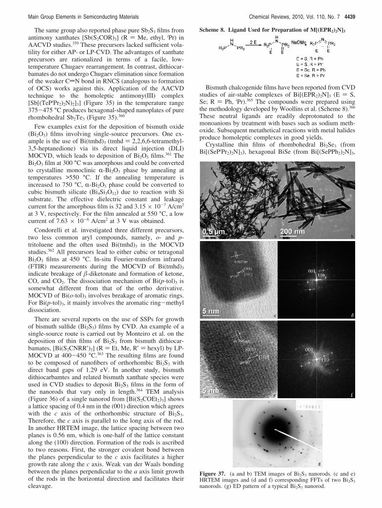
The same group also reported phase pure Sb2S3 films fromantimony xanthates [Sb(S2COR)3] (R ) Me, ethyl, iPr) inAACVD studies.359 These precursors lacked sufficient vola-tility for either AP- or LP-CVD. The advantages of xanthateprecursors are rationalized in terms of a facile, low-temperature Chugaev rearrangement. In contrast, dithiocar-bamates do not undergo Chugaev elimination since formationof the weaker CdN bond in RNCS (analogous to formationof OCS) works against this. Application of the AACVDtechnique to the homoleptic antimony(III) complex[Sb[(TePiPr2)2N)2]3] (Figure 35) in the temperature range375-475 °C produces hexagonal-shaped nanoplates of purerhombohedral Sb2Te3 (Figure 35).360
Few examples exist for the deposition of bismuth oxide(Bi2O3) films involving single-source precursors. One ex-ample is the use of Bi(tmhd)3 (tmhd ) 2,2,6,6-tetramethyl-3,5-heptanedione) via its direct liquid injection (DLI)MOCVD, which leads to deposition of Bi2O3 films.361 TheBi2O3 film at 300 °C was amorphous and could be convertedto crystalline monoclinic R-Bi2O3 phase by annealing attemperatures >550 °C. If the annealing temperature isincreased to 750 °C, R-Bi2O3 phase could be converted tocubic bismuth silicate (Bi4Si3O12) due to reaction with Sisubstrate. The effective dielectric constant and leakagecurrent for the amorphous film is 32 and 3.15 × 10⁻⁷ A/cm2
at 3 V, respectively. For the film annealed at 550 °C, a lowcurrent of 7.63 × 10⁻⁶ A/cm2 at 3 V was obtained.
Condorelli et al. investigated three different precursors,two less common aryl compounds, namely, o- and p-tritoluene and the often used Bi(tmhd)3 in the MOCVDstudies.362 All precursors lead to either cubic or tetragonalBi2O3 films at 450 °C. In-situ Fourier-transform infrared(FTIR) measurements during the MOCVD of Bi(tmhd)3
indicate breakage of -diketonate and formation of ketone,CO, and CO2. The dissociation mechanism of Bi(p-tol)3 issomewhat different from that of the ortho derivative.MOCVD of Bi(o-tol)3 involves breakage of aromatic rings.For Bi(p-tol)3, it mainly involves the aromatic ring-methyldissociation.
There are several reports on the use of SSPs for growthof bismuth sulfide (Bi2S3) films by CVD. An example of asingle-source route is carried out by Monteiro et al. on thedeposition of thin films of Bi2S3 from bismuth dithiocar-bamates, [Bi(S2CNRR′)3] (R ) Et, Me, R′ ) hexyl) by LP-MOCVD at 400-450 °C.363 The resulting films are foundto be composed of nanofibers of orthorhombic Bi2S3 withdirect band gaps of 1.29 eV. In another study, bismuthdithiocarbamtes and related bismuth xanthate species wereused in CVD studies to deposit Bi2S3 films in the form ofthe nanorods that vary only in length.364 TEM analysis(Figure 36) of a single nanorod from [Bi(S2COEt2)3] showsa lattice spacing of 0.4 nm in the (001) direction which agreeswith the c axis of the orthorhombic structure of Bi2S3.Therefore, the c axis is parallel to the long axis of the rod.In another HRTEM image, the lattice spacing between twoplanes is 0.56 nm, which is one-half of the lattice constantalong the (100) direction. Formation of the rods is ascribedto two reasons. First, the stronger covalent bond betweenthe planes perpendicular to the c axis facilitates a highergrowth rate along the c axis. Weak van der Waals bondingbetween the planes perpendicular to the a axis limit growthof the rods in the horizontal direction and facilitates theircleavage.
Bismuth chalcogenide films have been reported from CVDstudies of air-stable complexes of Bi[(EPR2)2N]3 (E ) S,Se; R ) Ph, iPr).365 The compounds were prepared usingthe methodology developed by Woollins et al. (Scheme 8).366
These neutral ligands are readily deprotonated to themonoanions by treatment with bases such as sodium meth-oxide. Subsequent metathetical reactions with metal halidesproduce homoleptic complexes in good yields.
Crystalline thin films of rhombohedral Bi2Se3 (fromBi[(SePiPr2)2N]3), hexagonal BiSe (from Bi[(SePPh2)2N]3,
Figure 37. (a and b) TEM images of Bi2S3 nanorods. (c and e)HRTEM images and (d and f) corresponding FFTs of two Bi2S3
nanorods. (g) ED pattern of a typical Bi2S3 nanorod.
Scheme 8. Ligand Used for Preparation of M[(EPR2)2N]3
Main Group Elements in Semiconducting Materials Chemical Reviews, 2010, Vol. 110, No. 7 4439

and orthorhombic Bi2S3 (from Bi[(SPR2)2N]3) have beendeposited on glass substrates.365 The suggested reason fordeposition of monophasic Bi2Se3 and BiSe from isopropyl-and phenyl-substituted precursors, respectively, is highlyspeculative. It may be that the difference in the electron-donating character of the alkyl group on the P atoms affectsthe relative bond strengths within the structures and hencethe decomposition profiles of the parent molecules. Thisaffect could potentially have a significant impact on therelative amounts of bismuth and selenium reaching, or beingretained at, the surface. Thin films composed of hexagonalBi2Se3 nanoplates have also been deposited from MOCVD
of bismuth diselenophosphato complex, [Bi(Se2POiPr)23],on modified and unmodified Si substrates.367 The depositedBi2Se3 nanoplates have a superior thermoelectric propertyover bulk Bi2Se3.
7.2. Precursors for V-VI NanoparticlesSeveral morphologies such as nanorods, nanocrystals, and
nanotapes of Bi2S3 are obtained from solvent thermolysis ofbismuth trisxanthates or bismuth dithiocarbamates in ethyleneglycol.364 The morphology of the Bi2S3 crystals dependedon the solvent used, the thermolysis temperature, and the
Table 1. Precursors Used for CVD of Thin Filmsa
precursor material technique substrate/growth temp (oC) ref
[Cd(SC6H2tBu3)2] CdS LP-MOCVD GaAs(111)/460 35
Zn[TeSi(SiMe3)3]2 ZnTe LP-MOCVD Si, InAs, GaAs/250-350 39[Cd(S2PMe2)2] CdS LP-MOCVD copper-, silver-, gold-coated glass/<500 43[Cd(S2PEt2)2] CdS LP-MOCVD glass, InP(111)/400 44[M(S2PiBu2)2]2 (M ) Cd, Zn) CdS, ZnS LP-MOCVD glass/400-450 45[M(S2CNEt2)2] (M ) Cd, Zn) CdS, ZnS LP-MOCVD glass, InP(100), GaAs(100)/350-400 64[Cd(S2CNEt2)2]/[Zn(S2CNEt2)2] ZnxCd1-xS LP-MOCVD glass, InP(100), GaAs(100)/400-420 64[Zn(Se2PMenHex)2]2 ZnSe LP-MOCVD glass/400-450 68[Cd(S2CNMenBu)2]2 CdS LP-MOCVD glass/450-500 71[Me2CdZn(Se2CNEt2)2] Cd0.5Zn0.5Se LP-MOCVD glass/450 75[M(SOCMe)2(tmeda)] (M ) Cd, Zn) CdS, ZnS, Cdl-xZnxS AACVD Si(100)/100-250 83[Cd(SOCNEt2)2] CdS LP-MOCVD glass, GaAs(100)/350-450 102[M(EPR2)2N2] (M ) Cd, Zn;E ) S, Se; R ) Ph, iPr)
CdS, CdSe, ZnS, ZnSe LP-MOCVD glass/400-525 110, 114
[MeCd(SePiPr2)2N]2 CdSe LP-MOCVD glass/425-450 115Cd[(TePiPr2)2N]2 CdTe AACVD glass/375-475 116
[Cd(msacmsac)2(NO3)2] CdS AACVD glass/450-500 122[Me2Ga(µ-AstBu2)]2 GaAs LP-MOCVD GaAs(100), GaAs(111),
R-Al2O3 (0001)/525250
[nBu2Ga(µ-AstBu2)]2 GaAs spray MOCVD GaAs(100)/520-540 259[Me2In-PtBu2]2 InP modified MBE InP(100)/480 260[Me2MSb(tBu)2]3 (M ) Ga, In) GaSb, InSb LP-MOCVD Si(100)/450 261[R2AlSb(SiMe3)2]2 (R ) Et, iBu) AlSb HV-CVD Si(100), Al2O3/325-550 262[tBuGaSbEt2] GaSb HV-CVD Si(100)/350-550 266nBuIn(SiPr) In2S3 MOCVD 250-400 287[tBuIn(µ-StBu)]2 InS AP-MOCVD Si(100), KBr/300-400 289Me2In(SePh) InSe spray MOCVD GaAs(100)/408-477 290In(SePh)3 In2Se3 spray MOCVD GaAs(100)/473-530 290[Me2InS2CNEt2] InS, In6S7, In2S3 LP-MOCVD GaAs(100)/350-425 291[In(S2CNMeR)3] (R ) nBu, nHex) In2S3 LP-MOCVD glass, GaAs(100),
InP(111)/450-500293
[In(S2COiPr)3] In2S3 295Ga(SCOMe)3(dmp) Ga2S3 AACVD 275-310 301b[In(µ-Te)[N(iPr2PTe)2]3 In2Te3 AACVD glass, Si(100)/325-475 302[Pb(S2CNRR′)2] (R ) Me, Et;R′ ) iPr, nBu)
PbS AACVD, LP-MOCVD glass/400-450 316
[Pb(EPiPr2)2N]2] (E ) Se, Te) PbSe, PbTe AACVD, LP-MOCVD glass/375-475 316, 317[SnCH(µ-SiMe3)22(-E)2 SnSe, SnTe LP-MOCVD Cu/Si, 300, 400 319, 320[Sn(OCH(CF3)2)4(NHMe2)2] SnOx LP-MOCVD glass, Si, quartz, 200-450 322Sn(OtBu)4 SnO2 LP-MOCVD quartz/500-700 327[SnCl4OC(H)OC2H52] SnO2 AP-CVD glass/360-560 329[Sn(SCH2CH2S)2] SnS AACVD glass/400-500 333[SnCl4o-C6H4(CH2SMe)2] SnS, SnS2 LP-CVD Si/600-650 336[SnCl4(Et2Se)2] SnSe2 LP-CVD Si/500-550 336Sb(OR)3 (R ) Et, nBu) Sb2O3 AP-CVD Si(111)/400-600 353, 354[Sb(O2CNMe2)3] Sb2O3 LP-CVD glass/380 355[Sb(S2CNMeR)3] (R ) Bu, Hex, Bz) Sb2S3 LP-MOCVD and
AACVDglass/<300 and g395,respectively
357
Sb(SR)3 (R ) tBu, CH2CF3) Sb2S3 LP-MOCVD glass, Si/300-450 358[Sb(S2COR)3] (R ) Me, Ethyl, iPr) Sb2S3 AACVD glass, Si/200-240 359Sb[N(PiPr2Te)2]3 Sb2Te3 AACVD glass/325-475 360Bi(tmhd)3 Bi2O3 DLI-MOCVD Si/225-425 361[Bi(S2CNRR′)3] (R,R′ ) ethyl,R ) methyl, R′ ) hexyl)
Bi2S3 LP-MOCVD glass/400-450 363
[Bi(S2COEt2)3] Bi2S3 LP-MOCVD Si(100)/400 364Bi(EPR2)2N3] (E ) S, Se; R ) Ph, iPr) BiSe, Bi2Se3, AACVD, LP-MOCVD glass/350-475 365[Bi(Se2POiPr)23] Bi2Se3 LP-MOCVD Si/350, 450 367
a TMEDA ) N,N,N,N-tetramethylethylenediamine; msacmsac ) dimorpholinodithioacetylacetonate; dmp ) 3,5-dimethylpyridine; tmhd ) 2,2,6,6-tetramethyl-3,5-hepatnedione; MBE ) molecular beam epitaxy; DLI ) direct liquid injection.
4440 Chemical Reviews, 2010, Vol. 110, No. 7 Malik et al.

nature of the precursor. The bismuth xanthates exhibited alower decomposition temperature (<150 °C) than the dithio-carbamate analogues (>200 °C). Precursors adopting thepolymeric structures in solution decompose at a highertemperature than those with dimeric structures. The outcomeis that polymeric [Bi(S2COiPr)3] give long Bi2S3 nanofibers,whereas dimeric [Bi(S2COR)3] (R ) alkyl) produce nano-crystals. Bi2S3 has the tendency to form nanorods relativelyeasily due to the inherent Bi-S chain-type structure. It isknown that Bi2S3 crystallizes with a lamellar structure withlinked Bi2S3 units forming infinite chains, which, in turn,are connected via van der Waals interactions.368 Formationof Bi2S3 nanorods originates from the preferential directionalgrowth of Bi2S3 crystallites along its c axis. Nanorods ofBi2S3 and Sb2S3 are also reported from hydrothermaldecomposition of [M(S2CNEt2)3] (M ) Bi, Sb).369 Waterexerts an influence on formation of M2S3 nanocrystals. Aproton and hydroxide anion from H2O may promote cleavageof one of the C-S bonds and S-M coordination bonds inthe precursors to form M2S3. Adducts of Bi(S2COsbutyl)3
with pyridine and 1,10-phenanthroline have also beenhydrothermally treated to deposit rods with diameters in therange of 20-35 nm and lengths up to several hundreds ofnanometers (Figure 37).370 When PVP is used instead ofneutral ligands, highly uniform Bi2S3 nanorods with anaverage diameter of 20 nm are produced. The optical bandedge of Bi2S3 nanorods from 1,10-phenanthroline derivativeis blue shifted with a band gap of ∼1.67 eV. High-qualityM2S3 nanorods are also reported by solvothermal treatmentof metal dithiophosphates [M(S2PnOctyl2)3] in the presenceof oleylamine.371
The conditions such as reaction time, temperature, andconcentration of precursors all play an important role indetermining the size and aspect ratio of the product. Vittaland co-workers reported various morphologies of Bi2S3
nanomaterials including nanorods, nanoleaves, nanoflowers,and dandelion-like structures through colloidal solution of[Bi(SCOPh)3].372 In the presence of both dodecanethiol andTOPO, Bi2S3 nanorods with an average diameter of 21.3 nm
and a length of 300 nm are reported. When the surfactant ischanged to dodecanethiol and oleylamine, Bi2S3 nanorodswith grooves are deposited. The oleylamine might haveplayed a key role in making grooves on the surface of Bi2S3
nanorods due to its corrosive nature. Previously amines havealso been used solely for etching purposes.373 In the presenceof polyvinylpyrrolidone and ethylene glycol, dandelion-shaped Bi2S3 nanostructures are obtained. It is possible forPVP to adsorb onto the surface of Bi2S3 branches throughnitrogen and oxygen atoms in the pyrrolidone groups andprompt formation of dandelion-like structures from individualBi2S3 wires due to its cross-linking ability.374 Production ofSb2Se3 nanowires from [SbSe2P(OiPr)23] under solvother-mal conditions has been reported.375 In a later study theauthors studied the electrical and optical properties of a singleSb2Se3 nanorod with an average size of 70 nm in diameterand a length of ∼1-2 µm.376
8. ConclusionsThis overview shows the contribution of main group
element chemistry in evolving the available and potentiallyuseful compound semiconductors as summarized in Tables1 and 2. Chemists have played a major role in the designand development of precursors and methods for depositingsemiconductor materials. The single-source approach is achemist’s answer to the problems posed by the use ofseparate sources. This review summarizes the use of differentfamilies of main group metal complexes that have been usedfor the preparation of potentially functional materials as thinfilms or nanoparticles. Several research groups have suc-cessfully designed and/or prepared such complexes. Mostof the single-source molecules have low volatilities, butvolatilities can be enhanced by various chemical modifica-tions. Liquid delivery methods (aerosol, spray, injection) havebeen increasingly used during the past decade which do notrequire a volatile precursor. In addition, the most commonmethod used for preparation of nanoparticles involvesthermolysis of the precursor in a high-boiling solvent which
Table 2. Precursors Used for the Growth of Nanocrystalsa
precursor material capping ligand growth temp (°C) morphology ref
[Cd(NH2CSNHNH2)2Cl2] CdS TOPO 280 nanorods 128[Cd(E2CNEt2)2] (E ) S, Se) CdS, CdSe pyridine, 4-ethylpyridine 167 nanocrystals 140[MeCdSe2CNEt2]2 CdSe TOPO 250 nanocrystals 144[Cd(E2CNMenHex)2] (E ) S, Se) CdSe/CdS TOPO 250 nanocrystals 158Ga(NH)3/2n GaN trioctylamine 360 nanocrystals 267[M(H2NCONH2)6]Cl3 (M ) Al, Ga) AlN, GaN trioctylamine 360 nanocrystals 271[(NH4)3In1-xGaxF6] InGaN ammonolysis (500) nanocrystals 274M(PtBu2)3 (M ) Ga, In) InP, GaP 4-ethylpyridine 167 nanocrystals 275, 276[X2GaP(SiMe3)2]2 (X ) Be, I) GaP pyrolysis (300) nanocrystals 277[H2GaE(SiMe3)2]3 (E ) P, As) GaP, GaAs pyrolysis (450 and 600) nanocrystals 278[tBu2AsInEt2]2 InAs HDA 280 nanocrystals 279[tBu2AsGaMes2]2 GaAs HDA 120 nanocrystals 280[(tBu)GaSe]4 GaSe APCVD KBr, Si(100)/325-335 nanocrystals 306[(EtMe2C)InSe]4 InSe APCVD KBr, Si(100)/290 nanocrystals 306[In(E2CNEt2)3] (E ) S, Se) InS, InSe 4-ethylpyridine, TOPO 250, 167 nanocrystals 307[Pb(S2CNEt2)2] PbS TOPO 250 nanocrystals 338[Pb(SCOC6H5)2] PbS alkylamines room temperature nanocrystals 343[Sn(S2CNEt2)2] SnS oleylamine 170 nanocrystals 352[M(S2CNEt2)3] (M ) Bi, Sb) Sb2S3, Bi2S3 water, chlorodform,
acetonitrile115-170 nanocrystals 369
[Bi(S2COC4H9)3(L)2](L ) pyridine, 1,10-phenanthroline)
Bi2S3 PVP 130-180 nanorods 370
[Bi(SCOPh)3] Bi2S3 TOPO, DT, PVP, EG,cysteine, ethylenediamine
150 nanorods 372
[SbSe2P(OiPr)23] Sb2Se3 methanol 100, 150 nanowires, nanorods 375
a PVP ) poly(vinyl pyrrolidone), DT ) dodecanethiol, EG ) ethylene glycol.
Main Group Elements in Semiconducting Materials Chemical Reviews, 2010, Vol. 110, No. 7 4441

again has nothing to do with the volatility of the precursor.Thus, the important factors to consider for the design ofprecursors are purity, stability, toxicity, ease of synthesis,and cost involved for synthesis.
Given the potential importance of these chalcogenides, inapplications as diverse as hybrid solar cells, sensors, etc.,we anticipate further commercial exploitation of suchprocesses in future years. We envisage that chemists willcontinue their interests with important objectives led by ourneed for sustainable process and energy sources, a need tominimize environmental impact, and a need for cost-effectiveprocesses for materials based on common (cheaper) elements.These objectives will be mirrored by technological needssuch as low-temperature processing (deposition on plastics)and higher and more reproducible optical and electronicproperties. The area remains one that is ripe for furtherdevelopment and discovery.
9. AcknowledgmentsThe authors would thank EPSRC, UK for financial
assistance. P.O.B. wrote this review while a visiting fellowat Magdalen College, Oxford. He would like to thank theCollege for the Fellowship and the President and Fellowsfor being gracious hosts.
10. References(1) Manasevit, H. M. J. Cryst. Growth 1981, 55, 1.(2) Hirata, S. Y.; Fujita, S.; Isenuera, M. J. Cryst. Growth 1990, 104,
521.(3) (a) Giapis, K. P.; Jensen, K. F. J. Cryst. Growth 1990, 101, 11–1.
(b) Giapis, K. P.; Lu, D. C.; Fotiadis, D. I.; Jensen, K. F. J. Cryst.Growth 1990, 104, 629.
(4) Foster, D. F.; Patterson, I. J.; James, L. D.; Cole-Hamilton, D. J.;Annitage, D. N.; Yates, H. M.; Wright, A. C.; Williams, J. O. AdV.Mater. Opt. Electron. 1994, 3, 163.
(5) Nishimura, K.; Nagao, Y.; Sakai, K. J. Cryst. Growth 1993, 134,293.
(6) (a) Kuhn, W.; Naumov, A.; Stanzl, H.; Bauer, S.; Wolf, K.; Wagner,H. P.; Gebhardt, W.; Pohl, U. W.; Krost, A.; Richter, W.; Dumichen,U.; Thiele, K. H. J. Cryst. Growth 1992, 123, 605. (b) Sato, G.;Numai, T.; Hoshiyama, M.; Suernune, I.; Machida, H.; Shimoyama,N. J. Cryst. Growth 1995, 150, 734.
(7) Hails, J. E.; Irvine, S. J. C.; Mullin, J. B.; Shenai-Khatkhate, D. V.;Cole-Hamilton, D. J. Mater. Res. Soc. Symp. Proc. 1989, 131, 75.
(8) Hails, J. E.; Irvine, S. J. C.; Mullin, J. B. Mater. Res. Soc. Symp.Proc. 1990, 162, 343.
(9) (a) Bell, W.; Stevenson, J.; Cole-Hamilton, D. J.; Hails, J. E.Polyhedron 1994, 13, 1253. (b) Stevenson, J.; Bell, W.; Ferry, J.;Cole-Hamilton, D. J.; Hails, I. E. J. Organomet. Chem. 1993, 449,141. (c) Hails, J. E.; Cole-Hamilton, D. J.; Bell, W. J. Cryst. Growth1994, 145, 596.
(10) Stringfellow, G. B. Organometallic Vapour Phase Epitaxy: Theoryand Practice; Academic Press: New York, 1989.
(11) Cole-Hamilton, D. J. Chem. Br. 1990, 852.(12) Mullin, J. B.; Irvine, S. J. C. Prog. Cryst. Growth Charact. 1994,
29, 217.(13) (a) Smith, L. M.; Thompson, J. Chemtronics 1989, 4, 60. (b) Mullin,
J. B.; Cole-Hamilton, D. J.; Irvine, S. J. C.; Hails, J. E.; Giess, J.;Gough, J. S. J. Cryst. Growth 1990, 101, 1.
(14) (a) O’Brien, P. In Inorganic Materials; Bruce, D. W., O’Hare, D.,Eds.; Wiley: Chichester, U.K., 1992; p 491. (b) O’Brien, P.Chemtronics 1991, 5, 61. (c) Jones, A. C.; Wright, P. J.; Cockayne,B. Chemtronics 1988, 3, 35.
(15) Wright, P. J.; Cockayne, B.; Parbrook, P. J.; Oliver, E. P.; Jones,A. C. J. Cryst. Growth 1991, 108, 525.
(16) Coates, G. E.; Ridley, D. J. Chem. Soc. 1965, 1870. (a) Adamson,G. W. Acta Crystallogr., Sect. B 1982, 38, 462.
(17) Malik, M. A.; Motevaili, M.; Walsh, J. R.; O’Brien, P.; Jones, A. C.J. Mater. Chem. 1995, 5, 731.
(18) Adamson, G. W.; Shearer, H. M. M. J. Chem. Soc., Chem. Commun.1969, 897.
(19) Zeng, D. H.; Hampden-Smith, M. J.; Duesler, E. N. Inorg. Chem.1994, 33, 5376.
(20) Bochmann, M. Chem. Vap. Deposition 1996, 2, 85.
(21) Hursthouse, M. B.; Motevalli, M.; O’Brien, P.; Walsh, J. R.; Jones,A. C. Organometallics 1991, 10, 3196.
(22) Dance, I. G. Polyhedron 1986, 5, 1037.(23) Hursthouse, M. B.; Khan, O. F. Z.; Mazid, M.; Motevalli, M.;
O’Brien, P. Polyhedron. 1990, 9, 541.(24) Khan, O. F. Z.; O’Brien, P. Polyhedron. 1991, 10, 325.(25) (a) Brennan, J. G.; Segrist, T.; Carroll, P. J.; Stuczynski, S. M.;
Reynders, P.; Brus, L. E.; Steigerwald, M. L. J. Am. Chem. Soc.1989, 111, 4141. (b) Chem. Mater. 1990, 2, 403.
(26) Osakada, K.; Yamamoto, T. J. Chem. Soc., Chem. Commun. 1987,117.
(27) Steigerwald, M. L.; Sprinkle, C. R. J. Am. Chem. Soc. 1987, 109,7200.
(28) Zeng, D.; Hampden-Smith, M. J.; Densler, E. N. lnorg. Chem. 1994,33, 5376.
(29) Blower, P. J.; Dilworth, J. R.; Hutchinson, J. P.; Zubieta, J. A.J. Chem. Soc., Dalton Trans. 1985, 1533.
(30) Bochmann, M.; Webb, K.; Harman, M.; Hursthouse, M. B. Angew.Chem., Int. Ed. Engl. 1990, 29, 638.
(31) Bochmann, M.; Webb, K. J.; Hursthouse, M. B.; Mazid, M. J. Chem.Soc., Dalton Trans. 1991, 2317.
(32) Bochmann, M.; Webb, K. J. J. Chem. Soc., Dalton Trans. 1991, 2325.(33) Bochmann, M.; Bwembya, G. C.; Grinter, R.; Powell, A. K.; Webb,
K. J.; Hursthouse, M. B.; Abdel Malik, K. M.; Mazid, M. A. Inorg.Chem. 1994, 33, 2290.
(34) Bochmann, M.; Webb, K. J. Mater. Res. Soc. Symp. Proc. 1991,204, 149. Chem. Abstr. 1992, 116, 3 3194h.
(35) Bochmann, M.; Webb, K. J.; Hails, J.-E.; Wolverson, D. Eur. J. SolidState lnorg. Chem. 1992, 29, 155.
(36) Bochmann, M.; Coleman, A. P.; Powell, A. K. Polyhedron 1992,11, 507.
(37) Dabbousi, B. O.; Bonasia, P. J.; Arnold, J. J. Am. Chem. Soc. 1991,113, 3186.
(38) Bonasi, P. J.; Arnold, J. Znorg. Chem. 1992, 31, 2508.(39) Arnold, J.; Walker, J. M.; Yu, K. M.; Bonasia, P. J.; Seligson, A. L.;
Bourret, E. D. J. Cryst. Growth 1992, 124, 647.(40) Bonasia, P. J.; Gindelberger, D. E.; Dabbousi, B. O.; Arnold, J. J. Am.
Chem. Soc. 1992, 114, 5209.(41) Bonasia, P. J.; Mitchell, G. P.; Hollander, F. J.; Arnold, J. Inorg.
Chem. 1994, 33, 1797.(42) Arnold, J. Bonasia, P. J. U.S. Patent 5157136, Oct 20, 1992.(43) Takahashi, Y.; Yuki, R.; Sugiura, M.; Motojima, S.; Sugiyama, K.
J. Cryst. Growth 1980, 50, 491.(44) Evans, M. A. H.; Williams, J. D. Thin Solid Films 1982, 87, L1.(45) Byrom, C.; Malik, M. A.; O’Brien, P.; White, A. J. P. Polyhedron
2000, 19, 211.(46) Haiduc, I.; Bryan-Sowerby, D.; Shao-Fang, L. Polyhedron 1995, 4,
3389.(47) Lawton, S. L.; Kokotailo, G. T. Inorg. Chem. 1969, 8, 2410.(48) Adeogun, A.; Nguyen, C. Q.; Afzaal, M.; Malik, M. A.; O’Brien, P.
Chem. Commun. 2006, 2179.(49) Nguyen, C. Q.; Adeogun, A.; Afzaal, M.; Malik, M. A.; O’Brien, P.
Chem. Commun. 2006, 2182.(50) Park, J.-H.; O’Brien, P.; White, A. J. P.; Williams, D. J. Inorg. Chem.
2001, 40, 3629.(51) Garcia-Montalvo, V.; Cea-Olivares, R.; Williams, D. J.; Espinosa-
Perez, G. Inorg. Chem. 1996, 35, 3948. Zaitseva, E. G.; Baidina,I. A.; Stabnikov, P. A.; Borisov, S. V.; Igumenov, I. K. Zh. Strukt.Khim. 1990, 31, 184.
(52) Dymock, K.; Palenok, G. J.; Slezak, J.; Raston, C. L.; White, A. H.J. Chem. Soc., Dalton. Trans. 1976, 28. Bhattacharya, S.; Seth, N.;Srivastava, D. K.; Gupta, V. D.; Noth, H.; Thomann-Albach, M.J. Chem. Soc., Dalton. Trans. 1996, 2815.
(53) Park, J.-H.; O’Brien, P.; White, A. J. P.; Williams, D. J. Inorg. Chem.2001, 40, 3629.
(54) Klug, H. P. Acta Crystallogr. 1966, 21, 536.(55) Bonamico, M.; Mazzone, G.; Vaciago, A.; Zambonelli, L. Acta
Crystallogr. 1965, 19, 898.(56) Miyame, H.; Ito, M.; Iwasaki, H. Acta Crystallogr. 1979, B35, 1480.(57) Domenicano, A.; Torelli, L.; Vaciago, A.; Zambonelli, L. J. Chem.
Soc. A 1968, 1351.(58) Bonamico, M.; Dessy, G. J. Chem. Soc. A 1971, 264.(59) Hursthouse, M. B.; Malik, M. A.; Motevalli, M.; O’Brien, P.
Polyhedron 1992, 11, 45.(60) Motevalli, M.; O’Brien, P.; Walsh, J. R.; Watson, I. M. Polyhedron
1996, 15, 2801.(61) Saunders, A.; Vecht, A.; Tyrell, G. Chem. Abstr. 1988, 108, 66226h.(62) Druz, B. L.; Evtukhov, Y. N.; Rakhlin, M. Y. Metallorg. Khim. 1988,
1, 645.(63) Druz, B. L.; Dyadenko, A. I.; Evtukhov, Y. N.; Rakhlin, M. Y.;
Rodionov, V. E. IzV. Akad. Nauk. SSSR, Neorg. Mater. 1990, 26,34.
4442 Chemical Reviews, 2010, Vol. 110, No. 7 Malik et al.
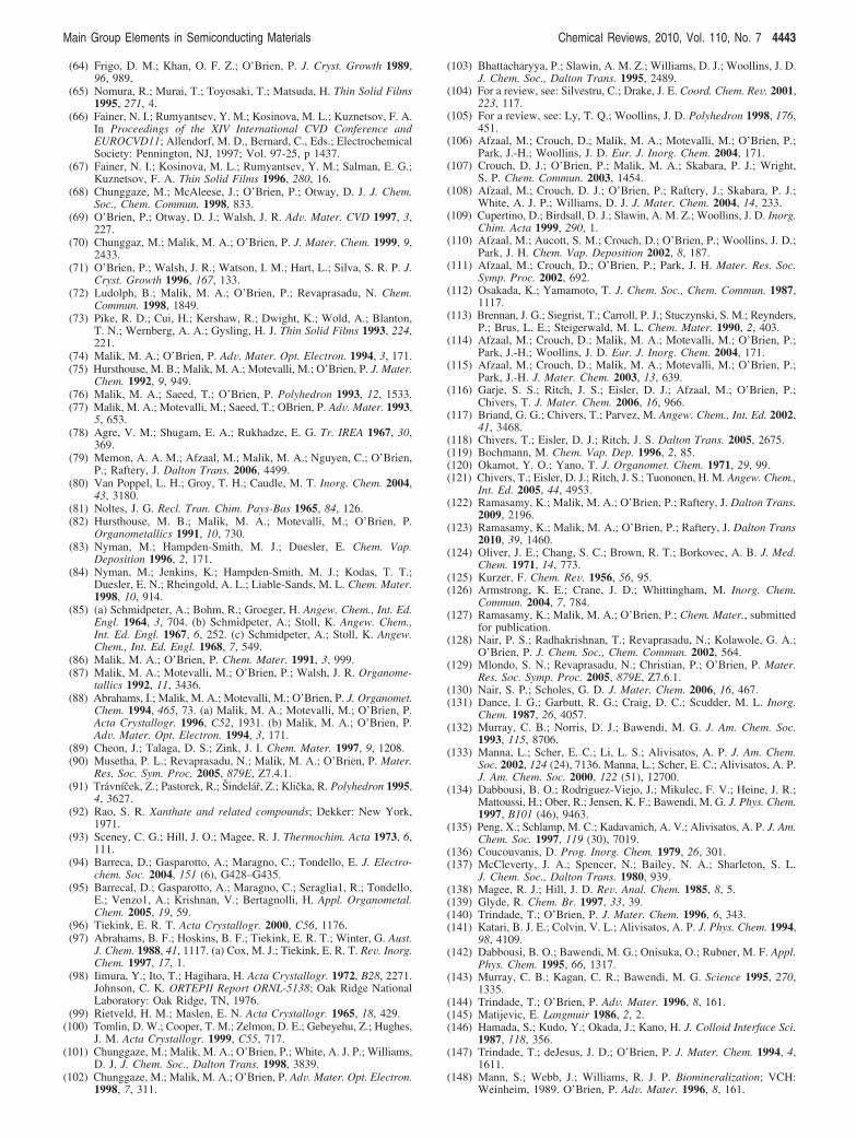
(64) Frigo, D. M.; Khan, O. F. Z.; O’Brien, P. J. Cryst. Growth 1989,96, 989.
(65) Nomura, R.; Murai, T.; Toyosaki, T.; Matsuda, H. Thin Solid Films1995, 271, 4.
(66) Fainer, N. I.; Rumyantsev, Y. M.; Kosinova, M. L.; Kuznetsov, F. A.In Proceedings of the XIV International CVD Conference andEUROCVD11; Allendorf, M. D., Bernard, C., Eds.; ElectrochemicalSociety: Pennington, NJ, 1997; Vol. 97-25, p 1437.
(67) Fainer, N. I.; Kosinova, M. L.; Rumyantsev, Y. M.; Salman, E. G.;Kuznetsov, F. A. Thin Solid Films 1996, 280, 16.
(68) Chunggaze, M.; McAleese, J.; O’Brien, P.; Otway, D. J. J. Chem.Soc., Chem. Commun. 1998, 833.
(69) O’Brien, P.; Otway, D. J.; Walsh, J. R. AdV. Mater. CVD 1997, 3,227.
(70) Chunggaz, M.; Malik, M. A.; O’Brien, P. J. Mater. Chem. 1999, 9,2433.
(71) O’Brien, P.; Walsh, J. R.; Watson, I. M.; Hart, L.; Silva, S. R. P. J.Cryst. Growth 1996, 167, 133.
(72) Ludolph, B.; Malik, M. A.; O’Brien, P.; Revaprasadu, N. Chem.Commun. 1998, 1849.
(73) Pike, R. D.; Cui, H.; Kershaw, R.; Dwight, K.; Wold, A.; Blanton,T. N.; Wernberg, A. A.; Gysling, H. J. Thin Solid Films 1993, 224,221.
(74) Malik, M. A.; O’Brien, P. AdV. Mater. Opt. Electron. 1994, 3, 171.(75) Hursthouse, M. B.; Malik, M. A.; Motevalli, M.; O’Brien, P. J. Mater.
Chem. 1992, 9, 949.(76) Malik, M. A.; Saeed, T.; O’Brien, P. Polyhedron 1993, 12, 1533.(77) Malik, M. A.; Motevalli, M.; Saeed, T.; OBrien, P. AdV. Mater. 1993,
5, 653.(78) Agre, V. M.; Shugam, E. A.; Rukhadze, E. G. Tr. IREA 1967, 30,
369.(79) Memon, A. A. M.; Afzaal, M.; Malik, M. A.; Nguyen, C.; O’Brien,
P.; Raftery, J. Dalton Trans. 2006, 4499.(80) Van Poppel, L. H.; Groy, T. H.; Caudle, M. T. Inorg. Chem. 2004,
43, 3180.(81) Noltes, J. G. Recl. Tran. Chim. Pays-Bas 1965, 84, 126.(82) Hursthouse, M. B.; Malik, M. A.; Motevalli, M.; O’Brien, P.
Organometallics 1991, 10, 730.(83) Nyman, M.; Hampden-Smith, M. J.; Duesler, E. Chem. Vap.
Deposition 1996, 2, 171.(84) Nyman, M.; Jenkins, K.; Hampden-Smith, M. J.; Kodas, T. T.;
Duesler, E. N.; Rheingold, A. L.; Liable-Sands, M. L. Chem. Mater.1998, 10, 914.
(85) (a) Schmidpeter, A.; Bohm, R.; Groeger, H. Angew. Chem., Int. Ed.Engl. 1964, 3, 704. (b) Schmidpeter, A.; Stoll, K. Angew. Chem.,Int. Ed. Engl. 1967, 6, 252. (c) Schmidpeter, A.; Stoll, K. Angew.Chem., Int. Ed. Engl. 1968, 7, 549.
(86) Malik, M. A.; O’Brien, P. Chem. Mater. 1991, 3, 999.(87) Malik, M. A.; Motevalli, M.; O’Brien, P.; Walsh, J. R. Organome-
tallics 1992, 11, 3436.(88) Abrahams, I.; Malik, M. A.; Motevalli, M.; O’Brien, P. J. Organomet.
Chem. 1994, 465, 73. (a) Malik, M. A.; Motevalli, M.; O’Brien, P.Acta Crystallogr. 1996, C52, 1931. (b) Malik, M. A.; O’Brien, P.AdV. Mater. Opt. Electron. 1994, 3, 171.
(89) Cheon, J.; Talaga, D. S.; Zink, J. I. Chem. Mater. 1997, 9, 1208.(90) Musetha, P. L.; Revaprasadu, N.; Malik, M. A.; O’Brien, P. Mater.
Res. Soc. Sym. Proc. 2005, 879E, Z7.4.1.(91) Travnıcek, Z.; Pastorek, R.; Sindelar, Z.; Klicka, R. Polyhedron 1995,
4, 3627.(92) Rao, S. R. Xanthate and related compounds; Dekker: New York,
1971.(93) Sceney, C. G.; Hill, J. O.; Magee, R. J. Thermochim. Acta 1973, 6,
111.(94) Barreca, D.; Gasparotto, A.; Maragno, C.; Tondello, E. J. Electro-
chem. Soc. 2004, 151 (6), G428–G435.(95) Barrecal, D.; Gasparotto, A.; Maragno, C.; Seraglia1, R.; Tondello,
E.; Venzo1, A.; Krishnan, V.; Bertagnolli, H. Appl. Organometal.Chem. 2005, 19, 59.
(96) Tiekink, E. R. T. Acta Crystallogr. 2000, C56, 1176.(97) Abrahams, B. F.; Hoskins, B. F.; Tiekink, E. R. T.; Winter, G. Aust.
J. Chem. 1988, 41, 1117. (a) Cox, M. J.; Tiekink, E. R. T. ReV. Inorg.Chem. 1997, 17, 1.
(98) Iimura, Y.; Ito, T.; Hagihara, H. Acta Crystallogr. 1972, B28, 2271.Johnson, C. K. ORTEPII Report ORNL-5138; Oak Ridge NationalLaboratory: Oak Ridge, TN, 1976.
(99) Rietveld, H. M.; Maslen, E. N. Acta Crystallogr. 1965, 18, 429.(100) Tomlin, D. W.; Cooper, T. M.; Zelmon, D. E.; Gebeyehu, Z.; Hughes,
J. M. Acta Crystallogr. 1999, C55, 717.(101) Chunggaze, M.; Malik, M. A.; O’Brien, P.; White, A. J. P.; Williams,
D. J. J. Chem. Soc., Dalton Trans. 1998, 3839.(102) Chunggaze, M.; Malik, M. A.; O’Brien, P. AdV. Mater. Opt. Electron.
1998, 7, 311.
(103) Bhattacharyya, P.; Slawin, A. M. Z.; Williams, D. J.; Woollins, J. D.J. Chem. Soc., Dalton Trans. 1995, 2489.
(104) For a review, see: Silvestru, C.; Drake, J. E. Coord. Chem. ReV. 2001,223, 117.
(105) For a review, see: Ly, T. Q.; Woollins, J. D. Polyhedron 1998, 176,451.
(106) Afzaal, M.; Crouch, D.; Malik, M. A.; Motevalli, M.; O’Brien, P.;Park, J.-H.; Woollins, J. D. Eur. J. Inorg. Chem. 2004, 171.
(107) Crouch, D. J.; O’Brien, P.; Malik, M. A.; Skabara, P. J.; Wright,S. P. Chem. Commun. 2003, 1454.
(108) Afzaal, M.; Crouch, D. J.; O’Brien, P.; Raftery, J.; Skabara, P. J.;White, A. J. P.; Williams, D. J. J. Mater. Chem. 2004, 14, 233.
(109) Cupertino, D.; Birdsall, D. J.; Slawin, A. M. Z.; Woollins, J. D. Inorg.Chim. Acta 1999, 290, 1.
(110) Afzaal, M.; Aucott, S. M.; Crouch, D.; O’Brien, P.; Woollins, J. D.;Park, J. H. Chem. Vap. Deposition 2002, 8, 187.
(111) Afzaal, M.; Crouch, D.; O’Brien, P.; Park, J. H. Mater. Res. Soc.Symp. Proc. 2002, 692.
(112) Osakada, K.; Yamamoto, T. J. Chem. Soc., Chem. Commun. 1987,1117.
(113) Brennan, J. G.; Siegrist, T.; Carroll, P. J.; Stuczynski, S. M.; Reynders,P.; Brus, L. E.; Steigerwald, M. L. Chem. Mater. 1990, 2, 403.
(114) Afzaal, M.; Crouch, D.; Malik, M. A.; Motevalli, M.; O’Brien, P.;Park, J.-H.; Woollins, J. D. Eur. J. Inorg. Chem. 2004, 171.
(115) Afzaal, M.; Crouch, D.; Malik, M. A.; Motevalli, M.; O’Brien, P.;Park, J.-H. J. Mater. Chem. 2003, 13, 639.
(116) Garje, S. S.; Ritch, J. S.; Eisler, D. J.; Afzaal, M.; O’Brien, P.;Chivers, T. J. Mater. Chem. 2006, 16, 966.
(117) Briand, G. G.; Chivers, T.; Parvez, M. Angew. Chem., Int. Ed. 2002,41, 3468.
(118) Chivers, T.; Eisler, D. J.; Ritch, J. S. Dalton Trans. 2005, 2675.(119) Bochmann, M. Chem. Vap. Dep. 1996, 2, 85.(120) Okamot, Y. O.; Yano, T. J. Organomet. Chem. 1971, 29, 99.(121) Chivers, T.; Eisler, D. J.; Ritch, J. S.; Tuononen, H. M. Angew. Chem.,
Int. Ed. 2005, 44, 4953.(122) Ramasamy, K.; Malik, M. A.; O’Brien, P.; Raftery, J. Dalton Trans.
2009, 2196.(123) Ramasamy, K.; Malik, M. A.; O’Brien, P.; Raftery, J. Dalton Trans
2010, 39, 1460.(124) Oliver, J. E.; Chang, S. C.; Brown, R. T.; Borkovec, A. B. J. Med.
Chem. 1971, 14, 773.(125) Kurzer, F. Chem. ReV. 1956, 56, 95.(126) Armstrong, K. E.; Crane, J. D.; Whittingham, M. Inorg. Chem.
Commun. 2004, 7, 784.(127) Ramasamy, K.; Malik, M. A.; O’Brien, P.; Chem. Mater., submitted
for publication.(128) Nair, P. S.; Radhakrishnan, T.; Revaprasadu, N.; Kolawole, G. A.;
O’Brien, P. J. Chem. Soc., Chem. Commun. 2002, 564.(129) Mlondo, S. N.; Revaprasadu, N.; Christian, P.; O’Brien, P. Mater.
Res. Soc. Symp. Proc. 2005, 879E, Z7.6.1.(130) Nair, S. P.; Scholes, G. D. J. Mater. Chem. 2006, 16, 467.(131) Dance, I. G.; Garbutt, R. G.; Craig, D. C.; Scudder, M. L. Inorg.
Chem. 1987, 26, 4057.(132) Murray, C. B.; Norris, D. J.; Bawendi, M. G. J. Am. Chem. Soc.
1993, 115, 8706.(133) Manna, L.; Scher, E. C.; Li, L. S.; Alivisatos, A. P. J. Am. Chem.
Soc. 2002, 124 (24), 7136. Manna, L.; Scher, E. C.; Alivisatos, A. P.J. Am. Chem. Soc. 2000, 122 (51), 12700.
(134) Dabbousi, B. O.; Rodriguez-Viejo, J.; Mikulec, F. V.; Heine, J. R.;Mattoussi, H.; Ober, R.; Jensen, K. F.; Bawendi, M. G. J. Phys. Chem.1997, B101 (46), 9463.
(135) Peng, X.; Schlamp, M. C.; Kadavanich, A. V.; Alivisatos, A. P. J. Am.Chem. Soc. 1997, 119 (30), 7019.
(136) Coucouvanis, D. Prog. Inorg. Chem. 1979, 26, 301.(137) McCleverty, J. A.; Spencer, N.; Bailey, N. A.; Sharleton, S. L.
J. Chem. Soc., Dalton Trans. 1980, 939.(138) Magee, R. J.; Hill, J. D. ReV. Anal. Chem. 1985, 8, 5.(139) Glyde, R. Chem. Br. 1997, 33, 39.(140) Trindade, T.; O’Brien, P. J. Mater. Chem. 1996, 6, 343.(141) Katari, B. J. E.; Colvin, V. L.; Alivisatos, A. P. J. Phys. Chem. 1994,
98, 4109.(142) Dabbousi, B. O.; Bawendi, M. G.; Onisuka, O.; Rubner, M. F. Appl.
Phys. Chem. 1995, 66, 1317.(143) Murray, C. B.; Kagan, C. R.; Bawendi, M. G. Science 1995, 270,
1335.(144) Trindade, T.; O’Brien, P. AdV. Mater. 1996, 8, 161.(145) Matijevic, E. Langmuir 1986, 2, 2.(146) Hamada, S.; Kudo, Y.; Okada, J.; Kano, H. J. Colloid Interface Sci.
1987, 118, 356.(147) Trindade, T.; deJesus, J. D.; O’Brien, P. J. Mater. Chem. 1994, 4,
1611.(148) Mann, S.; Webb, J.; Williams, R. J. P. Biomineralization; VCH:
Weinheim, 1989. O’Brien, P. AdV. Mater. 1996, 8, 161.
Main Group Elements in Semiconducting Materials Chemical Reviews, 2010, Vol. 110, No. 7 4443

(149) Revaprasadu, N.; Malik, M. A.; O’ Brien, P.; Zulu, M. M.; Wakefield,G. J. Mater. Chem. 1998, 8 (8), 1885.
(150) Malik, M. A.; Motevalli, M.; O’ Brien, P. Acta Crystallogr. 1996,C25, 1931.
(151) Leppert, V. L.; Risbud, S. H.; Fendorf, M. J. Philos. Mag. Lett. 1997,75, 29.
(152) Chestnoy, N.; Hull, R.; Brus, L. E. J. Chem. Phys. 1986, 85, 2237.(153) Li, G.; Nogami, M. J. Appl. Phys. 1994, 75, 4276.(154) Lazell, M.; Norager, S. J.; O’Brien, P.; Revaprasadu, N. Mater. Sci.
Eng. 2001, C16, 129.(155) Lazell, M.; O’Brien, P. Chem Commun. 1999, 2041.(156) Malik, M. A.; O’Brien, P. Ad. Mater. Opt. Electron. 1994, 3, 171.(157) Hursthouse, M. B.; Malik, M. A.; Motevalli, M.; O’Brien, P. J. Mater.
Chem. 1992, 9, 949.(158) Revaprasadu, N.; Malik, M. A.; O’Brien, P.; Wakefield, G. J. Chem.
Soc., Chem. Commun. 1999, 1573.(159) Malik, M. A.; Revaprasadu, N.; O’Brien, P. Chem. Mater. 2001, 13,
913.(160) Lazell, M. R.; O’Brien, P. J. Mater. Chem. 1999, 9, 1381.(161) Peng, Z. A.; Peng, X. G J. Am. Chem. Soc. 2001, 123, 183.(162) Dance, I. G.; Choy, A.; Scudder, M. L. J. Am. Chem. Soc. 1984,
106, 6285.(163) Lee, G. S. H.; Fisher, K. J.; Craig, D. C.; Scudder, M.; Dance, I. G.
J. Am. Chem. Soc. 1990, 112, 6435.(164) Cumberland, S. L.; Hanif, K. M.; Javier, A.; Khitrov, G. A.; Strouse,
G. F.; Woessner, S. M.; Yun, C. S. Chem. Mater. 2002, 14, 1576.(165) Sarigiannis, D.; Peck, J. D.; Kioseoglou, G.; Petrou, A.; Mountziaris,
T. J. Appl. Phys. Lett. 2002, 80 (21), 4024.(166) Moloto, M. J.; Malik, M. A.; O’Brien, P.; Motevalli, M.; Kolawoli,
G. A. Polyhedron 2003, 22, 595.(167) Sarigiannis, D.; Mountziaris, T. J.; Peck, J. D.; Kioseoglou, G.; Petrou,
A. Proceedings of the IEEE 27th International symposium oncompound semiconductors; IEEE: Piscataway, NJ, 2000; p 321.
(168) Kagan, C. R.; Murray, C. B.; Nirmal, M.; Bawendi, M. G. Phys.ReV. Lett. 1996, 76, 1517.
(169) Achermann, M.; Petruska, M. A.; Crooker, S. A.; Klimov, V. I. J.Phys. Chem. B 2003, 107, 13782.
(170) Pradhan, N.; Goorskey, D.; Thessing, J.; Peng, X. J. Am. Chem. Soc.2005, 127, 17586–17587.
(171) Empedocles, S. A.; Norris, D. J.; Bawendi, M. G. Phys. ReV. Lett.1996, 77, 3873.
(172) Li, J. J.; Wang, Y. A.; Guo, W.; Keay, J. C.; Mishima, T. D.; Johnson,M. B.; Peng, X. J. Am. Chem. Soc. 2003, 125, 12567.
(173) Colvin, V. L.; Schlamp, M. C.; Allvisatos, A. P. Nature 1994, 370,354.
(174) Klimov, V. I.; Mikhailovsky, A. A.; Xu, S.; Malko, A.; Hollingsworth,J. A.; Leatherdale, C. A.; Eisler, H.; Bawendi, M. G. Science 2000,290, 314.
(175) Lee, J.; Sundar, V. C.; Heine, J. R.; Bawendi, M. G. AdV. Mater.2000, 12, 1102–1105.
(176) Han, M.; Gao, X.; Su, J. Z.; Nie, S. Nat. Biotechnol. 2001, 19, 631–635.
(177) Revaprasadu, R.; Malik, M. A.; O’Brien, P. J. Mater. Res. 1999, 14,3237. Revaprasadu, R.; Malik, M. A.; O’Brien, P. Mater. Res. Soc.Symp. Proc. 1999, 536, 353.
(178) Bhargava, R. N.; Gallagher, D.; Nurmikko, A. Phys. ReV. Lett. 1994,72, 416.
(179) Gallagher, D.; Heady, W. E.; Racz, J. M.; Bhargava, R. N. J. Cryst.Growth 1994, 138, 970.
(180) Soo, Y. L.; Ming, Z. H.; Huang, S. W.; Kao, Y. H.; Bhargava, R. N.;Gallagher, D. Phys. ReV. 1994, B50, 7602.
(181) Sooklal, K.; Cullum, B. S.; Angel, S. M.; Murphy, C. J. J. Phys.Chem. 1994, 100, 4551.
(182) Wang, Y.; Herron, N.; Moller, K.; Bein, T. Solid State Commun.1991, 77, 33. Levy, L.; Feltin, N.; Ingert, D.; Pileni, M. P. J. Phys.Chem. 1997, B 101, 9153.
(183) Counio, G.; Gacoin, T.; Boilot, J. P. J. Phys. Chem. 1998, B 102,5237.
(184) Mikulec, F. V.; Kanu, M.; Bennati, M.; Hall, D. A.; Griffin, R. G.;Bawandi, M. G. J. Am. Chem. Soc. 2000, 122, 2532.
(185) Pradhan, N.; Peng, X. J. Am. Chem. Soc. 2007, 129, 3339.(186) Abdel-Hady, A.; Afzaal, M.; Malik, M. A.; O’Brien, P. Unpublished
work,(187) (a) Jones, A. C. Chem. Soc. ReV. 1997, 101. (b) Kuech, T. F.; Veuhoff,
E. J. Cryst. Growth 1984, 68, 148.(188) Thrush, E. J.; Cureton, C. G.; Trigg, J. M.; Stagg, J. P.; Butler, B. R.
Chemtronics 1987, 2, 62.(189) Stringfellow, G. B. J. Cryst. Growth 1990, 105, 260.(190) Lee, P. W.; Omstead, T. R.; McKennd, D. R.; Jensen, K. F. J. Cryst.
Growth 1988, 93, 134.(191) Larsen, C. A.; Buchan, N. I.; Li, S. H.; Stringfellow, G. B. J. Cryst.
Growth 1988, 93, 15.(192) Maury, F. AdV. Mater. 1991, 3, 542.
(193) Cowley, A. H.; Jones, R. A. Polyhedron 1994, 13, 1149.(194) O’Brien, P.; Haggata, S. AdV. Mater. Opt. Electron. 1995, 5, 117.(195) Benz, K. W.; Renz, H.; Weidlein, J.; Pilkuhn, M. H. J. Electron.
Mater. 1981, 10, 185.(196) Moss, R. H.; Evans, J. S. J. Cryst. Growth 1981, 55, 129.(197) Zaouk, A.; Salvetat, E.; Sakaya, J.; Maury, F.; Constant, G. J. Cryst.
Growth 1981, 55, 135.(198) Maury, F.; Combes, M.; Constant, G.; Carles, R.; Renucci, J. B. J.
Phys. (Paris) 1982, 1, 347.(199) Maury, F.; Combes, M.; Constant, G. Proceedings of the EU-
ROCVD4; Bloem, J., Verspui, G., Wolff, L. R., Eds.; Philips Centrefor Manufacturing Technology: Eindhoven, The Netherlands, 1983;p 257.
(200) Maury, F.; Constant, G. Polyhedron 1984, 3, 581.(201) Zaouk, A.; Constant, G. J. Phys. (Paris) 1982, C5, 43.(202) Maury, F.; Hammadi, A. E.; Constant, G. J. Cryst. Growth 1984,
68, 88.(203) Hammadi, A. E.; Maury, F.; Muller, G.; Bensoam, J.; Constant, G.
Acad. Sci. Paris, Ser. II 1984, 299, 1255.(204) Maury, F.; Hammadi, A. E. J. Cryst. Growth 1988, 91, 97.(205) Maury, F.; Hammadi, A. E. J. Cryst. Growth 1988, 91, 105.(206) Maury, F. In Transformation of Organometallics into Common and
Exotic Materials: Design and ActiVation; Laine, R. M., Ed.; NATOASI Series E; Martinus Nijhoff: The Netherlands 1988, 141, 195.
(207) Cowley, A. H.; Benac, B. L.; Ekerdt, J. G.; Jones, R. A.; Kidd, K. B.;Lee, J. Y.; Miller, J. E. J. Am. Chem. Soc. 1988, 110, 6248.
(208) Yoshida, S.; Misawa, S.; Fujii, Y.; Takada, S.; Hayakawa, H.; Gonda,S.; Itoch, A. J. Vac. Sci. Technol. 1979, 16, 990.
(209) Ho, K. L.; Jensen, K. F.; Hwang, J. W.; Gladfether, W. L.; Evans,J. F. J. Cryst. Growth 1991, 107, 376.
(210) Interrante, L. V.; Lee, W.; McConnell, M.; Lewis, N.; Hall, E. J.Electrochem. Soc. 1989, 136, 472.
(211) Bradely, D. C.; Frigo, D. M.; White, E. A. D. Eur. Pat. Appl. 1989;0 331 448Ep.
(212) Fischer, R. A.; Miehr, A.; Ambacher, O.; Metzger, T.; Born, E. J.Cryst. Growth 1997, 170, 139.
(213) Slack, G. A.; Tanzilli, R. A.; Pohl, R. O.; Vandersande, J. W. J.Phys. Chem. Solids 1987, 48, 641.
(214) Callahan, D. L.; Thomas, G. J. Am. Chem. Soc. 1990, 73, 2167.(215) Jones, A. C.; Rushworth, S. A.; Houlton, D. J.; Roberts, J. S.; Roberts,
V.; Whitehouse, C. R.; Critchlow, G. W. Chem. Vap. Deposition1996, 2, 5.
(216) Interrante, L. V.; Carpenter, L. E.; Whitmarsh, C.; Lee, W. Mater.Res. Soc. Symp. 1986, 73, 359.
(217) Kim, Y.; Kim, J.-H.; Park, J. E.; Bae, J. B.; Kim, B.; Park, J.-T.;Yu, K.-S.; Kim, Y. Thin Solid Films 1999, 339, 200.
(218) Joo, O.-S.; Jung, K.-D.; Cho, S.-H.; Kyoung, J.-H.; Ahn, C.-K.; Choi,C.-S.; Dong, Y.; Yun, H.; Han, S.-H. Chem. Vap. Deposition 2002,8, 273.
(219) Hoffman, D. M.; Rangarajan, S. P.; Athavale, S. D.; Economou, D. J.;Liu, J.-R.; Zheng, Z.; Chu, W.-K. J. Vac. Sci. Technol. A 1996, 14,306.
(220) Lakhotia, V.; Neumayer, D. A.; Cowley, A. H.; Jones, R. A.; Ekerdt,J. G. Chem. Mater. 1995, 7, 546.
(221) Kouvetakis, J.; Beach, D. Chem. Mater. 1989, 1, 476.(222) Neumayer, D. A.; Cowley, A. H.; Decken, A.; Jones, R. A.; Lakhotia,
V.; Ekerdt, J. G. J. Am. Chem. Soc. 1995, 117, 5893.(223) Fischer, R. A.; Miehr, A.; Herdtweck, E.; Mattner, M. R.; Ambacher,
O.; Metzger, T.; Born, E.; Weinkauf, S.; Pulham, C. R.; Parsons, S.Chem.sEur. J. 1996, 8, 1353.
(224) McMurran, J.; Kouvetakis, J.; Nesting, D. C.; Smith, D. J.; Nubbard,J. L. J. Am. Chem. Soc. 1998, 120, 5233.
(225) McMurran, J.; Kouvetakis, J.; Smith, D. J. Appl. Phys. Lett. 1999,74, 883.
(226) Frank, A. C.; Stowasser, F.; Stark, O.; Kwak, H.-T.; Sussek, H.; Rupp,A.; Pritzkow, H.; Ambacher, O.; Giersig, M.; Fischer, R. A. AdV.Mater. Opt. Electron. 1998, 8, 135.
(227) Devi, A.; Rogge, W.; Wohlfart, A.; Hipler, F.; Becker, H. W.; Fischer,R. A. Chem. Vap. Deposition 2000, 6, 245.
(228) Schafer, J.; Wolfrum, J.; Fischer, R. A.; Sussek, H. Chem. Phys.Lett. 1999, 300, 152.
(229) Sung, M. M.; Kim, C.; Yoo, S. H.; Kim, C. G.; Kim, Y. Chem. Vap.Deposition 2002, 8, 50.
(230) Lee, J. H.; Yoo, S. H.; Lee, Y. K.; Kim, C. G.; Yang, Y. S.; Kim,Y.; Jeon, H. J. Korean Phys. Soc. 2001, 39, S242.
(231) Song, S.; Lee, S. S.; Yu, S. H.; Chung, T.-M.; Kim, C. G.; Lee,S.-B.; Kim, Y. Bull. Korean Chem. Soc. 2003, 24, 953.
(232) Guo, Q.; Kato, O.; Yoshida, A. J. Appl. Phys. 1993, 1, 7969.(233) Schaefer, J.; Wolfrum, J.; Fischer, R. A.; Sussek, H. Chem. Vap.
Deposition 1999, 5, 205.(234) Bae, B.-J.; Park, J. E.; Kim, B.; Park, J. T. J. Orgamet. Chem. 2000,
616, 128.(235) Saitosh, H.; Yarbrough, W. A. Diamond Relat. Mater. 1992, 1, 137.
4444 Chemical Reviews, 2010, Vol. 110, No. 7 Malik et al.

(236) Boo, J. H.; Rohr, C.; Ho, W. Phys. Status Solidi 1999, 176, 705.(237) Boo, J. H.; Lee, S.-B.; Yu, K.-S.; Kim, Y.; Kim, Y.-S.; Park, J. T.
J. Korean Phys. Soc. 1999, 34, 532.(238) Lorrette, C.; Weisbecker, P.; Jacques, S.; Pailler, R.; Goyheneche,
J. M. J. Eur. Ceram. Soc. 2007, 27, 2737.(239) Beachley, O. T.; Coates, G. E. J. Chem. Soc. 1965, 3241.(240) Beachley, O. T.; Kopasz, J. P.; Zhang, H.; Hunter, W. E.; Atwood,
J. L. J. Organomet. Chem. 1987, 325, 69.(241) Cowley, A. H.; Jones, R. A. Angew. Chem., Int. Ed. Engl. 1989, 28,
1208.(242) Arif, A. M.; Benac, B. L.; Cowley, A. H.; Greets, R.; Jones, R. A.;
Kidd, K. B.; Power, J. M.; Schwab, S. T. J. Chem. Soc., Chem.Commun. 1986, 1543.
(243) Arif, A. M.; Benac, B. L.; Cowley, A. H.; Jones, R. A.; Kidd, K. B.;Nunn, C. M. New J. Chem. 1988, 12, 553.
(244) Maury, F.; Combes, M.; Constant, G.; Carles, R.; Renucci, J. B. J.Phys. (Paris) 1982, 45, C1–347.
(245) Maury, F.; Constant, G. Polyhedron 1984, 3, 581.(246) Pitt, C. G.; Higa, K. T.; McPhail, A. T.; Wells, R. L. Inorg. Chem.
1986, 25, 2483.(247) Wells, R. L.; Purdy, A. P.; Higa, K. T.; McPhail, A. T.; Pitt, C. G.
J. Organomet. Chem. 1987, 325, C7.(248) Purdy, A. P.; Wells, R. L.; McPhail, A. T.; Pitt, C. G. Organometallics
1987, 6, 2099.(249) Malik, M. A.; O’Brien, P.; Norigar, S.; Smith, J. J. Mater. Chem.
2003, 13, 2591.(250) Miller, J. E.; Kidd, K. B.; Cowley, A. H.; Jones, R. A.; Ekerdt, J. G.;
Gysling, H. J.; Wernberg, A. A.; Blanton, T. N. Chem. Mater. 1990,2, 589.
(251) Miller, J. E.; Ekerdt, J. G. Chem. Mater. 1992, 4, 7.(252) Ekerdt, J. G.; Sun, Y. M.; Jackson, M. S.; Lakhotia, V.; Pacheco,
K. A.; Koschmieder, S. U.; Cowley, A. H.; Jones, R. A. J. Cryst.Growth 1992, 124, 158.
(253) O’Conner, D.; Phillips, D. Time-Correlated Single Photon Counting;Academic: London, 1984.
(254) Malik, M. A.; Afzaal, M.; O’Brien, P.; Bangert, U.; Hamilton, B.Mater. Sci. Technol. 2004, 20, 959.
(255) Malik, M. A.; O’Brien, P.; Halliwell, M. J. Mater. Chem. 2005, 15,2.
(256) Miller, J. E.; Mardones, M. A.; Nail, J. W.; Cowley, A. H.; Jones,R. A.; Ekerdt, J. G. Chem. Mater. 1992, 4, 447.
(257) Cowley, A. H.; Jones, R. A.; Mardones, M. A.; Nunn, C. M.Organometallics 1991, 10, 1635.
(258) Lu, J.-P.; Raj, R.; Wernberg, A. Thin Solid Films 1991, 205, 236.(259) Wernberg, A. A.; Lawrence, D. J.; Gysling, H. J.; Filo, A. J.; Blanton,
T. N. J. Cryst. Growth 1993, 131, 176.(260) Andrews, D. A.; Davies, G. J.; Bradley, D. C.; Faktor, M. M.; Frigo,
D. M.; White, E. A. D. Semicond. Sci. Technol. 1988, 3, 1053.(261) Cowley, A. H.; Jones, R. A.; Nunn, C. M.; Westmorland, D. L. Chem.
Mater. 1990, 2, 221.(262) Park, H. S.; Schulz, S.; Wessel, H.; Roesky, H. W. Chem. Vap.
Deposition 1999, 5, 179.(263) Kuczkowski, A.; Schulz, S.; Nieger, M.; Saarenketo, P. Organome-
tallics 2001, 20, 2000.(264) Kuczkowski, A.; Fahrenholz, S.; Schulz, S.; Nieger, M. Organome-
tallics 2004, 23, 3615.(265) Schuchmann, D.; Kuczkowski, A.; Fahrenholz, S.; Schulz, S.; Florke,
U. Eur. J. Inorg. Chem. 2007, 7, 931.(266) Schulz, S.; Fahrenholz, S.; Kuczkowski, A.; Assenmacher, W.;
Seemayer, A.; Hommes, A.; Wandelt, K. Chem. Mater. 2005, 17,1982.
(267) Micic, O. I.; Ahrenkiel, S. P.; Bertram, D.; Nozik, A. J. Appl. Phys.Lett. 1999, 75, 478.
(268) Coffer, J. L.; Johnson, M. A.; Zhang, L.; Wells, R. L.; Janik, J. F.Chem. Mater. 1997, 9, 2671.
(269) Manz, A.; Birkner, A.; Kolbe, M.; Fischer, R. A. AdV. Mater. 2000,12, 569.
(270) Pan, G.; Kordesch, M. E.; Patten, P. G. V. Chem. Mater. 2006, 18,3915.
(271) Sardar, K.; dan, M.; Schwenzer, B.; Rap, C. N. R. J. Mater. Chem.2005, 15, 2175.
(272) Schofield, P. S.; Zhou, W.; Wood, P.; Samuel, I. D. W.; Cole-Hamilton, D. J. J. Mater. Chem. 2004, 14, 3124.
(273) Choi, J.; Gillan, E. G. J. Mater. Chem. 2006, 16, 3774.(274) Schwenzer, B.; Meier, C.; Masala, O.; Seshadri, R.; DenBaars, S. P.;
Mishra, U. K. J. Mater. Chem 2005, 15, 1891.(275) Green, M.; O’Brien, P. Chem. Commun. 1998, 2459.(276) Green, M.; O’Brien, P. J. Mater. Chem. 2004, 14, 629.(277) Well, R. L.; Self, M. F.; McPhail, A. T.; Aubuchon, S. R.;
Woudenberg, R. C.; Jasinski, J. P. Organommetallics 1993, 12, 2832.(278) Janik, J. F.; Wells, R. L.; Young, V. G.; Rheingold, A. L.; Guzei,
L. A. J. Am. Chem. Soc. 1998, 120, 532.
(279) Malik, M. A.; O’Brien, P.; Helliwell, M. J. Mater. Chem. 2005, 15,1463.
(280) Malik, M. A.; Afzaal, M.; Brien, P.; Bangert, U.; Hamilton, B. Mater.Sci. Technol. 2004, 20, 959.
(281) Maschke, K.; Levy, F. Physics of Non-tetrahedrally Bonded BinaryCompounds. In Landolt-Bornstein New Series; Madelung, O., vonder Ostem, W., Rossler, U. , Eds.; Springer: Verlag, Berlin, 1983;Vol. 17f, Chapter 9.7. MacKinnon. A. Physics of Non-tetrahedrallyBonded Ternary Compounds. In Landolt-Bornstein New Series;Madelung, O., von der Ostem, W., Rossler, U., Eds.; Springer Verlag:Berlin, 1985; Vol. 17h, Chapter 10.1; pp 12-23.
(282) Nomura, R.; Inazawa, S. J.; Kanaya, K.; Matsuda, H. Polyhedron1989, 8, 763.
(283) Nomura, R.; Fujii, S.; Kanaya, K.; Matsuda, H. Polyhedron 1990, 9,361.
(284) Tuck, D. G. In ComprehensiVe Organometallic Chemistry; Wilkinson,G., Stone, F. G. A.; Abel, E. W., Eds.; Pergamon: Oxford, 1995.
(285) Nomura, R.; Inazawa, S. J.; Kanaya, K.; Matsuda, H. Appl.Organomet. Chem. 1989, 3, 195.
(286) Nomura, R.; Konishi, K.; Matsuda, H. Thin Solid Films 1991, 198,339.
(287) Nomura, R.; Konishi, K.; Matsuda, H. J. Electrochem. Soc. 1991,138, 631.
(288) MacInnes, A. N.; Power, M. B.; Barron, A. R. Adu. Mater. Opt.Electron. 1992, 1, 229.
(289) MacInnes, A. N.; Power, M. B.; Hepp, A. F.; Barron, A. R. J.Organomet. Chem. 1993, 449, 95.
(290) Gysling, H. J.; Wernberg, A. A.; Blanton, T. N. Chem. Mater. 1992,4, 900.
(291) Haggata, S. W.; Malik, M. A.; Motevalli, M.; O’Brien, P.; Knowles,J. C. Chem. Mater. 1995, 7, 716.
(292) O’Brien, P.; Otway, D. J.; Walsh, J. R. Chem. Vap. Deposition 1997,3, 227.
(293) O’Brien, P.; Otway, D. J.; Walsh, J. R. Thin Solid Films 1998, 315,57.
(294) Afzaal, M.; Malik, M. A.; O’Brien, P. Chem. Commun. 2004, 334.(295) Bessergenev, V. G.; Ivanova, E. N.; Kovalevskaya, Y. A.; Gromilov,
S. A.; Kirichenko, V. N.; Larionov, S. V. Inorg. Mater. 1996, 32,592.
(296) McAleese, J.; O’Brien, P.; Otway, D. J. Chem. Vap. Deposition 1998,4, 94.
(297) Horley, G. A.; Chunggaze, M.; O’Brien, P.; White, A. J. P.; Williams,D. J. J. Chem. Soc., Dalton Trans. 1998, 4205.
(298) Horley, G. A.; O’Brien, P.; Park, J.-H.; White, A. J. P.; Williams,D. J. J. Mater. Chem. 1999, 9, 1289.
(299) Kunze, K.; Bihry, L.; Atanasova, P.; Hampden-Smith, M. J.; Duesler,E. N. Chem. Vap. Deposition 1996, 2, 105.
(300) Shang, G.; Hampden-Smith, M. J.; Duesler, E. N. Chem. Commun.1996, 1733.
(301) (a) Shang, G.; Kunze, K.; Hampden-Smith, M. J.; Duesler, E. Chem.Vap. Deposition 1996, 2, 242. (b) Shang, G.; Hampden-Smith, M. J.;Duesler, E. N. Chem. Commun 1996, 1733.
(302) Garje, S. S.; Copsey, M. C.; Afzaal, M.; O’Brien, P.; Chiversb, T. J.Mater. Chem. 2006, 16, 4542.
(303) Copsey, M. C.; Chivers, T. Chem. Commun. 2005, 4938.(304) Dimitrijevic, N. M.; Kamat, P. V. Langmuir 1987, 3, 1004.(305) Kamat, P. V.; Dimitrijevic, N. M.; Fessenden, R. W. J. Phys. Chem.
1988, 92, 2324.(306) Stoll, S. L.; Gillan, E. G.; Barron, A. G. Chem. Vap. Deposition 1996,
2, 182.(307) Revaprasadu, N.; Malik, M. A.; Carstens, J.; O’Brien, P. J. Mater.
Chem. 1999, 9, 2885.(308) Chikan, V.; Kelly, D. F. Nano Lett. 2002, 2, 141.(309) levy, F. Crystallography and Crystal Chemistry of Materials with
Layered Structures; Reidel: Holland, 1976.(310) Stoll, S. L.; Gillan, E. G.; Barron, A. Chem. Vap. Deposition 1996,
2, 182. Gillan, E. G.; Barron, A. R. Chem. Mater. 1997, 9, 3037.Gillan, E. G.; Bott, S. G.; Barron, A. Chem. Mater. 1997, 9, 796.
(311) Dutta, D. P.; Sharma, G.; Ghoshal, S.; Prasad, N.; Jain, V. K. J.Nanosci. Nanotechnol. 2006, 6, 1.
(312) Ghoshal, S.; Kushwah, N. P.; Dutta, D. P.; Jain, V. K. Appl.Organomet. Chem. 2005, 19, 257.
(313) Dutta, D. P.; Sharma, G.; Tyagi, A. K.; Kulshreshtha, S. K. Mat.Sci. Eng. 2007, B138, 60.
(314) Fainer, N. I.; Kosinova, M. L.; Rumyantsev, Y. M.; Salman, E. G.;Kuznetsnov, F. A. Thin Solid Films 1996, 280, 16.
(315) Trindade, T.; O’Brien, P. Chem. Vap. Deposition 1997, 3, 75.(316) Afzaal, M.; Ellwood, K.; Pickett, N. L.; O’Brien, P.; Raftery, J.;
Waters, J. J. Mater. Chem. 2004, 14, 1310.(317) Ritch, J. S.; Ahmad, K.; Afzaal, M.; Chivers, T.; O’Brien, P. Inorg.
Chem. 2010, 49, 1158.(318) Akhtar, J.; Bruce, J. C.; Malik, M. A.; Klaus, R. K.; Afzaal, M.;
O’Brien, P. Mater. Res. Soc. Symp. Proc. 2009, 1148-PP12-08.
Main Group Elements in Semiconducting Materials Chemical Reviews, 2010, Vol. 110, No. 7 4445
(319) Chuprakov, I. S.; Dahmen, K.-H.; Schneider, J. J.; Hagen, J. Chem.Mater. 1998, 10, 3467.
(320) Chuprakov, I. S.; Dahmen, K.-H. J. Phys. IV 1999, 9, 313.(321) Schneider, J. J.; Hagen, J.; Heinemann, O.; Bruckmann, J.; Kruger,
C. Thin Solid Films 1997, 304, 144.(322) Suh, S.; Hoffman, D. M.; Atagi, L. M.; Smith, D. C.; Liu, J.-R.;
Chu, W.-K. Chem. Mater. 1997, 9, 730.(323) Houlton, D. J.; Jones, A. C.; Hycock, P. W.; Williams, E. W.; Bull,
J.; Critchlow, G. W. Chem. Vap. Deposition 1995, 1, 26.(324) Brown, J. R.; Cheney, M. T.; Hycock, P.; Houlton, D. J.; Jones, A. C.;
Williams, E. W. J. Electrochem. Soc. 1997, 144, 295.(325) Boyle, T. J.; Alam, T. M.; Rodriguez, M. A.; Zechmann, C. A. Inorg.
Chem. 2002, 41, 25742.(326) Boyle, T. J.; Ward, T. L.; De’Angeli, S. M.; Xu, H.; Hammetter,
W. F. Chem. Mater. 2003, 15, 765.(327) Mathur, S.; Sivakov, V.; Shen, H.; Barth, S.; Cavelius, C.; Nilsson,
A.; Kuhn, P. Thin Solid Films 2006, 502, 88.(328) kai, G.; Baik, N. S.; Miura, N.; Yamazoe, N. Sens. Actuators B:
Chem. 2001, 77, 116.(329) Talaty, N. N.; Beck, K.; Citeau, H.; Kirschbaum, K.; Giolando,
D. M. Z. Anorg. Allg. Chem 2009, 635, 53.(330) Mahon, M. F.; Molloy, K. C.; Stanley, J. E.; Rankin, D. W. H.;
Robertson, H. E.; Johnston, B. F. Appl. Organomet. Chem. 2005,19, 658.
(331) Hibbert, T. G.; Mahon, M. F.; Molloy, K. C.; Price, L. S.; Parkin,I. P. J. Mater. Chem. 2001, 11, 469.
(332) Barone, G.; Hibbert, T. G.; Mahon, M. F.; Molloy, K. C.; Price,L. S.; Parkin, I. P.; Hardy, A. M. E.; Field, M. N. J. Mater. Chem.2001, 11, 464.
(333) Parkin, I. P.; Price, L. S.; Hibbert, T. G.; Molloy, K. C. J. Mater.Chem. 2001, 11, 1486.
(334) Kana, A. T.; Hibbert, T. G.; Mahon, M. F.; Molloy, K. C.; Parkin,I. P.; Price, L. S. Polyhedron 2001, 20, 2989.
(335) Bade, B. P.; Garje, S. S.; Niwate, Y. S.; Afzaal, M.; O’Brien, P.Chem. Vap. Deposition 2008, 14, 292.
(336) Reid, S. D.; Hector, A. L.; Levason, W.; Reid, G.; Waller, B. J.;Webster, M. Dalton Trans. 2007, 4769.
(337) Chen, T.; Hunks, W.; Chen., P. S.; Stauf, G. T.; Cameron, T. M.;Xu, C.; DiPasuale, A. G.; Rheingold, A. L. Eur. J. Inorg. Chem.2009, 2047.
(338) Trindade, T.; O’Brien, P.; Zhang, X.-M.; Motevalli, M. J. Mater.Chem. 1997, 7, 1011.
(339) Trindade, T.; Monteiro, O. C.; O’Brien, P.; Motevalli, M. Polyhedron1999, 18, 1171.
(340) Lee, S.-M.; Jun, Y.-W.; Cho, S.-N.; Cheon, J. J. Am. Chem. Soc.2002, 124, 11244.
(341) Duan, T.; Lou, W.; Wang, X.; Xue, Q. Colloid Surf. A: Physicochem.Eng. Asp. 2007, 310, 86.
(342) Lee, S. M.; Cho, S. N.; Cheon, J. AdV. Mater. 2003, 15, 441.(343) Zhihua, Z.; Lee, S. H.; Vittal, J. J.; Chin, W. S. J. Phys. Chem. B
2006, 110, 6649.(344) Pradhan, N.; Katz, B.; Efrima, S. J. Phys. Chem. B 2003, 107, 13843.(345) Acharya, S.; Gautam, U. J.; Sasaki, T.; Bando, Y.; Golan, Y.; Ariga,
K. J. Am. Chem. Soc. 2008, 10, 4594.(346) Machol, J. L.; Wise, F. W.; Patel, R. C.; Tanner, D. B. Phys. ReV. B
1993, 48, 2819.(347) Krauss, T. D.; Wise, F. W. Phys. ReV. B 1997, 55, 9860.
(348) Krauss, T. D.; Wise, F. W.; Tanner, D. B. Phys. ReV. Lett. 1996, 76,1376.
(349) Luther, J. M.; Zheng, H.; Sadtler, B.; Alivisatos, A. P. J. Am. Chem.Soc. 2009, 131, 16851.
(350) Berhanu, D.; Govender, K.; Smyth-Boyle, D.; Archbold, M.; Halliday,D. P.; O’Brien, P. Chem. Commun. 2006, 4709.
(351) Sun, J.; Buhro, W. E. Angew. Chem., Int. Ed. 2008, 47, 3215.(352) Koktysh, D. S.; McBride, J. R.; Rosenthal, S. J. Nanoscale Res. Lett.
2007, 2, 144.(353) Haycock, P. W.; Horley, G. A.; Molloy, K. C.; Myers, C. P.;
Rushworth, S. A.; Smith, L. M. J. Phys. IV 2001, 11, Pr-3–1045.(354) Haycock, P. W.; Horley, G. A.; Molloy, K. C.; Myers, C. P.;
Rushworth, S. A.; Smith, L. M. Chem. Vap. Deposition 2001, 7, 191.(355) Horley, G. A.; Mahon, M. F.; Molloy, K. C.; Haycock, P. W.; Myers,
C. P. Inorg. Chem. 2002, 41, 5052.(356) Myers, C. P.; Haycock, P. W.; Pichot, M.; Horley, G. A.; Molloy,
K. C.; Rushworth, S. A.; Smith, L. M. Chem. Vap. Deposition 2004,10, 35.
(357) Rodriguez-Castro, J.; Mahon, M. F.; Molloy, K. C. Chem. Vap.Deposition 2006, 12, 601.
(358) Rodriguez-Castro, J.; Dale, P.; Mahon, M. F.; Molloy, K. C.; Peter,L. M. Chem. Mater. 2007, 19, 3219.
(359) Rodriguez-Castro, J.; Molloy, K. C.; Liu, Y.; Lai, C. S.; Dong, Z.;White, T. J.; Tiekink, E. R. T. J. Mater. Chem. 2008, 18, 5399.
(360) Garje, S. S.; Eisler, D. J.; Ritch, J. S.; Afzaal, M.; O’Brien, P.;Chivers, T. J. Am. Chem. Soc. 2006, 128, 3120.
(361) Kang, S. W.; Rhee, S. W. Thin Solid Films 2004, 468, 79.(362) Bedoya, C.; Condorelli, G. G.; Finocchiaro, S. T.; Di Mauro, A.;
Fragala, I. L.; Cattaneo, L.; Carella, S. Chem. Vap. Deposition 2005,11, 261.
(363) Monteiro, O. C.; Trindade, T.; Park, J.-H.; O’Brien, P. Chem. Vap.Deposition 2000, 6, 230.
(364) Koh, Y. W.; Lai, C. S.; Du, A. Y.; Tiekink, E. R. T.; Loh, K. P.Chem. Mater. 2003, 15, 4544.
(365) Waters, J.; Crouch, D.; Raftery, J.; O’Brien, P. Chem. Mater. 2004,16, 3289.
(366) Cupertino, D.; Birdsall, D. J.; Slawin, A. M. Z.; Woollins, J. D. Inorg.Chem. Acta 1999, 290, 1.
(367) Lin, Y.-F.; Chang, H.-W.; Lu, S.-Y.; Liu, C. W. J. Phys. Chem. C2007, 111, 18538.
(368) Arivuoli, D.; Gnanam, F. D.; Ramasamy, P. J. Mater. Sci. Lett. 1988,7, 711.
(369) Xie, G.; Qiao, Z.-P.; Zeng, M.-H.; Chen, X.-M.; Gao, S.-L. Cryst.Growth Des. 2004, 4, 513.
(370) Han, Q.; Chen, J.; Yang, X.; Lu, L.; Wang, X. J. Phys. Chem. C2007, 111, 14072.
(371) Lou, W.; Chen, M.; Wang, X.; Liu, W. Chem. Mater. 2007, 19, 872.(372) Tian, L.; Tan, H. Y.; Vittal, J. J. Cryst. Growth Des 2008, 8, 734.(373) Li, R. F.; Lee, J.; Yang, B. C.; Horspool, D. N.; Aindow, M.;
Papadimitrakopoulos, F. J. Am. Chem. Soc. 2005, 127, 2524.(374) Spalla, O.; Nabavi, M.; Minter, J.; Cabane, B. Colloid Polym. Sci.
1996, 274, 555.(375) Chang, H.-W.; Sarkar, B.; Liu, C. W. Cryst. Growth. Des. 2007, 7,
2691.(376) Ko, T. Y.; Yang, C. H.; Sun, K. W.; Chang, H. W.; Sarker, B.; Liu,
C. W. Cent. Eur. J. Chem. 2009, 7, 197.
CR900406F
4446 Chemical Reviews, 2010, Vol. 110, No. 7 Malik et al.