
Precision, Dual-Channel Instrumentation Amplifier AD8222 · The AD8222 is a dual-channel, high...
24
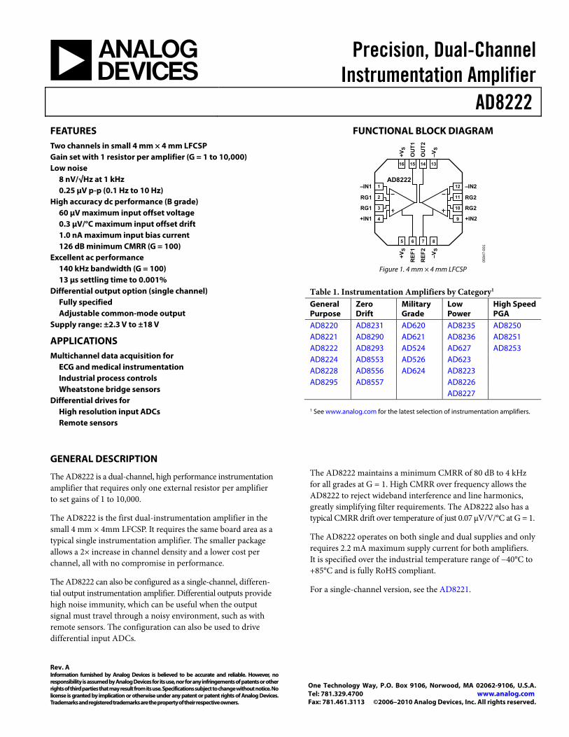
Precision, Dual-Channel Instrumentation Amplifier AD8222 Rev. A Information furnished by Analog Devices is believed to be accurate and reliable. However, no responsibility is assumed by Analog Devices for its use, nor for any infringements of patents or other rights of third parties that may result from its use. Specifications subject to change without notice. No license is granted by implication or otherwise under any patent or patent rights of Analog Devices. Trademarks and registered trademarks are the property of their respective owners. One Technology Way, P.O. Box 9106, Norwood, MA 02062-9106, U.S.A. Tel: 781.329.4700 www.analog.com Fax: 781.461.3113 ©2006–2010 Analog Devices, Inc. All rights reserved. FEATURES Two channels in small 4 mm × 4 mm LFCSP Gain set with 1 resistor per amplifier (G = 1 to 10,000) Low noise 8 nV/√Hz at 1 kHz 0.25 μV p-p (0.1 Hz to 10 Hz) High accuracy dc performance (B grade) 60 μV maximum input offset voltage 0.3 μV/°C maximum input offset drift 1.0 nA maximum input bias current 126 dB minimum CMRR (G = 100) Excellent ac performance 140 kHz bandwidth (G = 100) 13 μs settling time to 0.001% Differential output option (single channel) Fully specified Adjustable common-mode output Supply range: ±2.3 V to ±18 V APPLICATIONS Multichannel data acquisition for ECG and medical instrumentation Industrial process controls Wheatstone bridge sensors Differential drives for High resolution input ADCs Remote sensors FUNCTIONAL BLOCK DIAGRAM AD8222 1 2 3 4 12 11 10 9 5 6 7 8 13 14 15 16 –IN1 RG1 RG1 +IN1 –IN2 RG2 RG2 +IN2 +V S REF1 REF2 –V S +V S OUT1 OUT2 –V S 05947-001 Figure 1. 4 mm × 4 mm LFCSP Table 1. Instrumentation Amplifiers by Category 1 General Purpose Zero Drift Military Grade Low Power High Speed PGA AD8220 AD8231 AD620 AD8235 AD8250 AD8221 AD8290 AD621 AD8236 AD8251 AD8222 AD8293 AD524 AD627 AD8253 AD8224 AD8553 AD526 AD623 AD8228 AD8556 AD624 AD8223 AD8295 AD8557 AD8226 AD8227 1 See www.analog.com for the latest selection of instrumentation amplifiers. GENERAL DESCRIPTION The AD8222 is a dual-channel, high performance instrumentation amplifier that requires only one external resistor per amplifier to set gains of 1 to 10,000. The AD8222 is the first dual-instrumentation amplifier in the small 4 mm × 4mm LFCSP. It requires the same board area as a typical single instrumentation amplifier. The smaller package allows a 2× increase in channel density and a lower cost per channel, all with no compromise in performance. The AD8222 can also be configured as a single-channel, differen- tial output instrumentation amplifier. Differential outputs provide high noise immunity, which can be useful when the output signal must travel through a noisy environment, such as with remote sensors. The configuration can also be used to drive differential input ADCs. The AD8222 maintains a minimum CMRR of 80 dB to 4 kHz for all grades at G = 1. High CMRR over frequency allows the AD8222 to reject wideband interference and line harmonics, greatly simplifying filter requirements. The AD8222 also has a typical CMRR drift over temperature of just 0.07 μV/V/°C at G = 1. The AD8222 operates on both single and dual supplies and only requires 2.2 mA maximum supply current for both amplifiers. It is specified over the industrial temperature range of −40°C to +85°C and is fully RoHS compliant. For a single-channel version, see the AD8221.
Transcript of Precision, Dual-Channel Instrumentation Amplifier AD8222 · The AD8222 is a dual-channel, high...
Precision, Dual-ChannelInstrumentation Amplifier
AD8222
Rev. A Information furnished by Analog Devices is believed to be accurate and reliable. However, no responsibility is assumed by Analog Devices for its use, nor for any infringements of patents or other rights of third parties that may result from its use. Specifications subject to change without notice. No license is granted by implication or otherwise under any patent or patent rights of Analog Devices. Trademarks and registered trademarks are the property of their respective owners.
One Technology Way, P.O. Box 9106, Norwood, MA 02062-9106, U.S.A.Tel: 781.329.4700 www.analog.com Fax: 781.461.3113 ©2006–2010 Analog Devices, Inc. All rights reserved.
FEATURES Two channels in small 4 mm × 4 mm LFCSP Gain set with 1 resistor per amplifier (G = 1 to 10,000) Low noise
8 nV/√Hz at 1 kHz 0.25 μV p-p (0.1 Hz to 10 Hz)
High accuracy dc performance (B grade) 60 μV maximum input offset voltage 0.3 μV/°C maximum input offset drift 1.0 nA maximum input bias current 126 dB minimum CMRR (G = 100)
Excellent ac performance 140 kHz bandwidth (G = 100) 13 μs settling time to 0.001%
Differential output option (single channel) Fully specified Adjustable common-mode output
Supply range: ±2.3 V to ±18 V
APPLICATIONS Multichannel data acquisition for
ECG and medical instrumentation Industrial process controls Wheatstone bridge sensors
Differential drives for High resolution input ADCs Remote sensors
FUNCTIONAL BLOCK DIAGRAM
AD82221
2
3
4
12
11
10
9
5 6 7 8
13141516
–IN1
RG1
RG1
+IN1
–IN2
RG2
RG2
+IN2
+V
S
RE
F1
RE
F2
–VS
+V
S
OU
T1
OU
T2
–VS
059
47-0
01
Figure 1. 4 mm × 4 mm LFCSP
Table 1. Instrumentation Amplifiers by Category1 General Purpose
Zero Drift
Military Grade
Low Power
High SpeedPGA
AD8220 AD8231 AD620 AD8235 AD8250 AD8221 AD8290 AD621 AD8236 AD8251 AD8222 AD8293 AD524 AD627 AD8253 AD8224 AD8553 AD526 AD623 AD8228 AD8556 AD624 AD8223 AD8295 AD8557 AD8226 AD8227
1 See www.analog.com for the latest selection of instrumentation amplifiers.
GENERAL DESCRIPTION
The AD8222 is a dual-channel, high performance instrumentation amplifier that requires only one external resistor per amplifier to set gains of 1 to 10,000.
The AD8222 is the first dual-instrumentation amplifier in the small 4 mm × 4mm LFCSP. It requires the same board area as a typical single instrumentation amplifier. The smaller package allows a 2× increase in channel density and a lower cost per channel, all with no compromise in performance.
The AD8222 can also be configured as a single-channel, differen-tial output instrumentation amplifier. Differential outputs provide high noise immunity, which can be useful when the output signal must travel through a noisy environment, such as with remote sensors. The configuration can also be used to drive differential input ADCs.
The AD8222 maintains a minimum CMRR of 80 dB to 4 kHz for all grades at G = 1. High CMRR over frequency allows the AD8222 to reject wideband interference and line harmonics, greatly simplifying filter requirements. The AD8222 also has a typical CMRR drift over temperature of just 0.07 μV/V/°C at G = 1.
The AD8222 operates on both single and dual supplies and only requires 2.2 mA maximum supply current for both amplifiers. It is specified over the industrial temperature range of −40°C to +85°C and is fully RoHS compliant.
For a single-channel version, see the AD8221.
AD8222
Rev. A | Page 2 of 24
TABLE OF CONTENTS Features .............................................................................................. 1
Applications ....................................................................................... 1
Functional Block Diagram .............................................................. 1
General Description ......................................................................... 1
Revision History ............................................................................... 2
Specifications ..................................................................................... 3
Absolute Maximum Ratings ............................................................ 6
Thermal Resistance ...................................................................... 6
ESD Caution .................................................................................. 6
Pin Configuration and Function Descriptions ............................. 7
Typical Performance Characteristics ............................................. 8
Theory of Operation ...................................................................... 15
Amplifier Architecture .............................................................. 15
Gain Selection ............................................................................. 15
Reference Terminal .................................................................... 16
Package Considerations ............................................................. 16
Layout .......................................................................................... 16
Input Bias Current Return Path ............................................... 17
Input Protection ......................................................................... 18
RF Interference ........................................................................... 18
Common-Mode Input Voltage Range ..................................... 18
Applications Information .............................................................. 19
Differential Output .................................................................... 19
Driving a Differential Input ADC ............................................ 20
Precision Strain Gage ................................................................. 20
Driving Cabling .......................................................................... 21
Outline Dimensions ....................................................................... 22
Ordering Guide .......................................................................... 23
REVISION HISTORY 2/10—Rev. 0 to Rev. A Added LFCSP_VQ, CP-16-13 Package ............................ Universal Changes to Features Section and Table 1 ...................................... 1 Changed VIN+ to V+IN, VIN− to V−IN, and T to TA Throughout ..... 3 Change to Reference Input Parameter, Table 2 ............................. 4 Changed Output Short-Circuit Current to Output Short-Circuit Duration, Table 5 .............................................................................. 6 Changes to Thermal Resistance Section and Table 6 ................... 6 Changes to Figure 2 .......................................................................... 7 Changes to Figure 19 ...................................................................... 10 Changes to Figure 43 ...................................................................... 14
Changes to Reference Terminal Section, Figure 45, and Package Considerations Section .................................................................. 16 Deleted Thermal Pad Section ....................................................... 16 Added Package Without Thermal Pad and Package with Thermal Pad Sections .................................................................... 16 Changes to Figure 46 ...................................................................... 17 Deleted Solder Wash Section ........................................................ 17 Changes to RFI and Antialising Filter Section ........................... 20 Updated Outline Dimensions ....................................................... 22 Changes to Ordering Guide .......................................................... 23 7/06—Revision 0: Initial Version
AD8222
Rev. A | Page 3 of 24
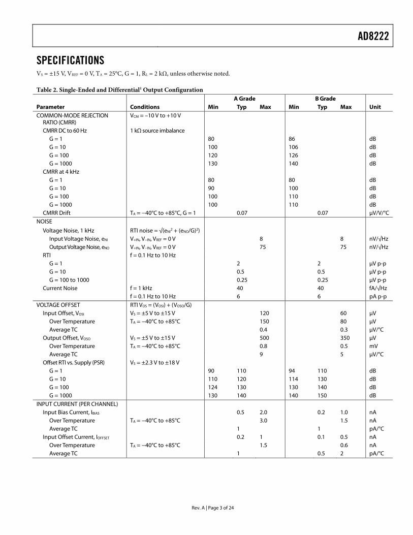
SPECIFICATIONS VS = ±15 V, VREF = 0 V, TA = 25°C, G = 1, RL = 2 kΩ, unless otherwise noted.
Table 2. Single-Ended and Differential1 Output Configuration A Grade B Grade Parameter Conditions Min Typ Max Min Typ Max Unit COMMON-MODE REJECTION
RATIO (CMRR) VCM = –10 V to +10 V
CMRR DC to 60 Hz 1 kΩ source imbalance G = 1 80 86 dB G = 10 100 106 dB G = 100 120 126 dB G = 1000 130 140 dB
CMRR at 4 kHz G = 1 80 80 dB G = 10 90 100 dB G = 100 100 110 dB G = 1000 100 110 dB
CMRR Drift TA = −40°C to +85°C, G = 1 0.07 0.07 μV/V/°C NOISE
Voltage Noise, 1 kHz RTI noise = √(eNI2 + (eNO/G)2)
Input Voltage Noise, eNI V+IN, V−IN, VREF = 0 V 8 8 nV/√Hz Output Voltage Noise, eNO V+IN, V−IN, VREF = 0 V 75 75 nV/√Hz
RTI f = 0.1 Hz to 10 Hz G = 1 2 2 μV p-p G = 10 0.5 0.5 μV p-p G = 100 to 1000 0.25 0.25 μV p-p
Current Noise f = 1 kHz 40 40 fA/√Hz f = 0.1 Hz to 10 Hz 6 6 pA p-p
VOLTAGE OFFSET RTI VOS = (VOSI) + (VOSO/G) Input Offset, VOSI VS = ±5 V to ±15 V 120 60 μV
Over Temperature TA = −40°C to +85°C 150 80 μV Average TC 0.4 0.3 μV/°C
Output Offset, VOSO VS = ±5 V to ±15 V 500 350 μV Over Temperature TA = −40°C to +85°C 0.8 0.5 mV Average TC 9 5 μV/°C
Offset RTI vs. Supply (PSR) VS = ±2.3 V to ±18 V G = 1 90 110 94 110 dB G = 10 110 120 114 130 dB G = 100 124 130 130 140 dB G = 1000 130 140 140 150 dB
INPUT CURRENT (PER CHANNEL) Input Bias Current, IBIAS 0.5 2.0 0.2 1.0 nA
Over Temperature TA = −40°C to +85°C 3.0 1.5 nA Average TC 1 1 pA/°C
Input Offset Current, IOFFSET 0.2 1 0.1 0.5 nA Over Temperature TA = −40°C to +85°C 1.5 0.6 nA Average TC 1 0.5 2 pA/°C
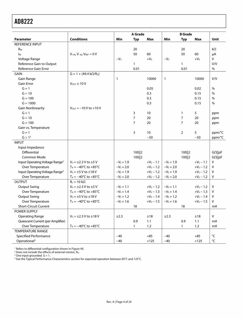
AD8222
Rev. A | Page 4 of 24
A Grade B Grade Parameter Conditions Min Typ Max Min Typ Max Unit REFERENCE INPUT
RIN 20 20 kΩ IIN V+IN, V−IN, VREF = 0 V 50 60 50 60 μA Voltage Range −VS +VS −VS +VS V Reference Gain to Output 1 1 V/V Reference Gain Error 0.01 0.01 %
GAIN G = 1 + (49.4 kΩ/RG) Gain Range 1 10000 1 10000 V/V Gain Error VOUT ± 10 V
G = 1 0.05 0.02 % G = 10 0.3 0.15 % G = 100 0.3 0.15 % G = 1000 0.3 0.15 %
Gain Nonlinearity VOUT = –10 V to +10 V G = 1 3 10 1 5 ppm G = 10 7 20 7 20 ppm G = 100 7 20 7 20 ppm
Gain vs. Temperature G = 1 3 10 2 5 ppm/°C G > 12 −50 −50 ppm/°C
INPUT Input Impedance
Differential 100||2 100||2 GΩ||pF Common Mode 100||2 100||2 GΩ||pF
Input Operating Voltage Range3 VS = ±2.3 V to ±5 V −VS + 1.9 +VS − 1.1 −VS + 1.9 +VS − 1.1 V Over Temperature TA = −40°C to +85°C −VS + 2.0 +VS − 1.2 −VS + 2.0 +VS − 1.2 V
Input Operating Voltage Range3 VS = ±5 V to ±18 V −VS + 1.9 +VS − 1.2 −VS + 1.9 +VS − 1.2 V Over Temperature TA = −40°C to +85°C −VS + 2.0 +VS − 1.2 −VS + 2.0 +VS − 1.2 V
OUTPUT RL = 10 kΩ Output Swing VS = ±2.3 V to ±5 V −VS + 1.1 +VS − 1.2 −VS + 1.1 +VS − 1.2 V
Over Temperature TA = −40°C to +85°C −VS + 1.4 +VS − 1.3 −VS + 1.4 +VS − 1.3 V Output Swing VS = ±5 V to ±18 V −VS + 1.2 +VS − 1.4 −VS + 1.2 +VS − 1.4 V
Over Temperature TA = −40°C to +85°C −VS + 1.6 +VS − 1.5 −VS + 1.6 +VS − 1.5 V Short-Circuit Current 18 18 mA
POWER SUPPLY Operating Range VS = ±2.3 V to ±18 V ±2.3 ±18 ±2.3 ±18 V Quiescent Current (per Amplifier) 0.9 1.1 0.9 1.1 mA
Over Temperature TA = −40°C to +85°C 1 1.2 1 1.2 mA TEMPERATURE RANGE
Specified Performance −40 +85 −40 +85 °C Operational4 −40 +125 −40 +125 °C
1 Refers to differential configuration shown in Figure 49. 2 Does not include the effects of external resistor, RG. 3 One input grounded. G = 1. 4 See the Typical Performance Characteristics section for expected operation between 85°C and 125°C.
AD8222
Rev. A | Page 5 of 24
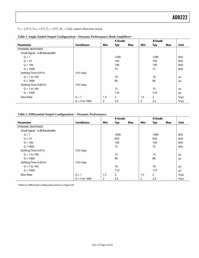
VS = ±15 V, VREF = 0 V, TA = 25°C, RL = 2 kΩ, unless otherwise noted.
Table 3. Single-Ended Output Configuration—Dynamic Performance (Both Amplifiers) A Grade B Grade Parameter Conditions Min Typ Max Min Typ Max Unit DYNAMIC RESPONSE
Small Signal −3 dB Bandwidth G = 1 1200 1200 kHz G = 10 750 750 kHz G = 100 140 140 kHz G = 1000 15 15 kHz
Settling Time 0.01% 10 V step G = 1 to 100 10 10 μs G = 1000 80 80 μs
Settling Time 0.001% 10 V step G = 1 to 100 13 13 μs G = 1000 110 110 μs
Slew Rate G = 1 1.5 2 1.5 2 V/μs G = 5 to 1000 2 2.5 2 2.5 V/μs
Table 4. Differential Output Configuration1—Dynamic Performance A Grade B Grade Parameter Conditions Min Typ Max Min Typ Max Unit DYNAMIC RESPONSE
Small Signal −3 dB Bandwidth G = 1 1000 1000 kHz G = 10 650 650 kHz G = 100 140 140 kHz G =1000 15 15 kHz
Settling Time 0.01% 10 V step G = 1 to 100 15 15 μs G = 1000 80 80 μs
Settling Time 0.001% 10 V step G = 1 to 100 18 18 μs G = 1000 110 110 μs
Slew Rate G = 1 1.5 2 1.5 2 V/μs G = 5 to 1000 2 2.5 2 2.5 V/μs
1 Refers to differential configuration shown in Figure 49.
AD8222
Rev. A | Page 6 of 24
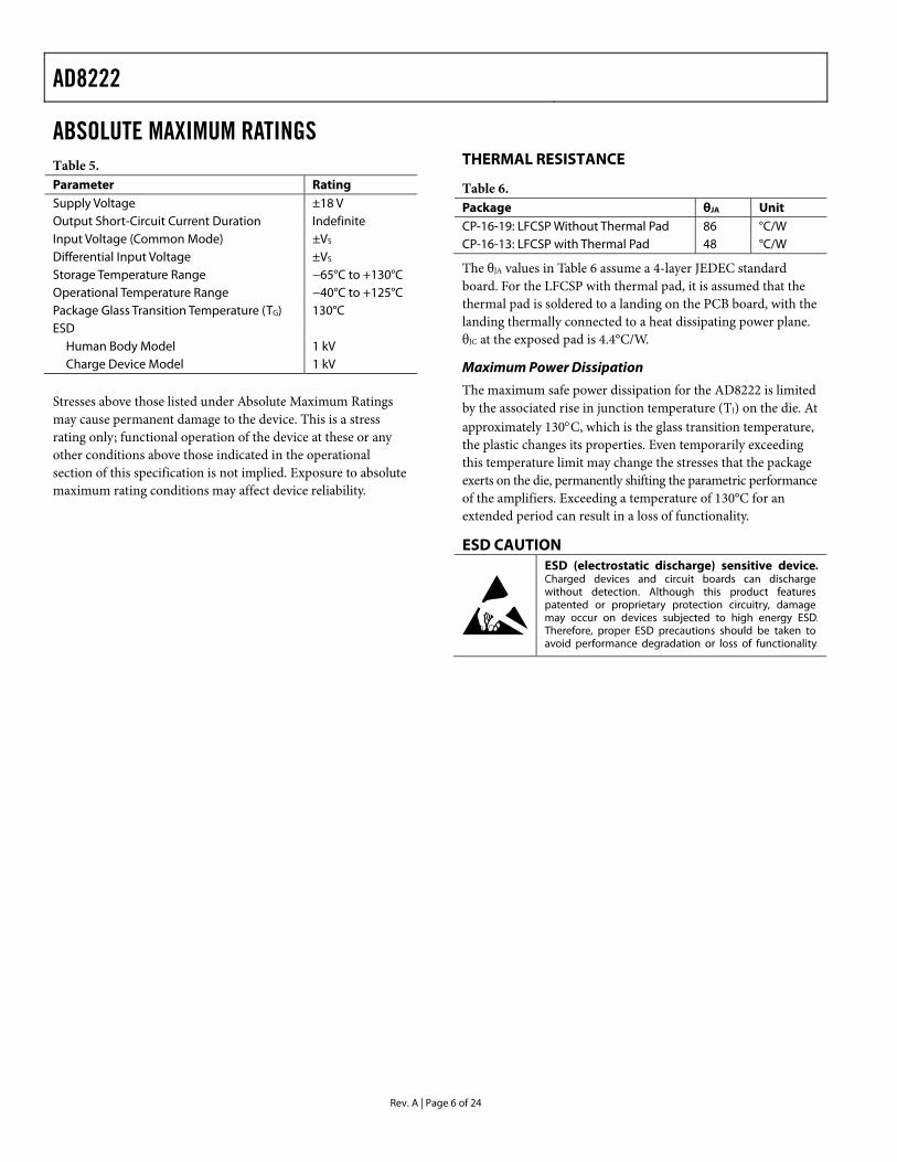
ABSOLUTE MAXIMUM RATINGS Table 5. Parameter Rating Supply Voltage ±18 V Output Short-Circuit Current Duration Indefinite Input Voltage (Common Mode) ±VS Differential Input Voltage ±VS Storage Temperature Range −65°C to +130°C Operational Temperature Range −40°C to +125°C Package Glass Transition Temperature (TG) 130°C ESD
Human Body Model 1 kV Charge Device Model 1 kV
Stresses above those listed under Absolute Maximum Ratings may cause permanent damage to the device. This is a stress rating only; functional operation of the device at these or any other conditions above those indicated in the operational section of this specification is not implied. Exposure to absolute maximum rating conditions may affect device reliability.
THERMAL RESISTANCE
Table 6. Package θJA Unit CP-16-19: LFCSP Without Thermal Pad 86 °C/W CP-16-13: LFCSP with Thermal Pad 48 °C/W
The θJA values in Table 6 assume a 4-layer JEDEC standard board. For the LFCSP with thermal pad, it is assumed that the thermal pad is soldered to a landing on the PCB board, with the landing thermally connected to a heat dissipating power plane. θJC at the exposed pad is 4.4°C/W.
Maximum Power Dissipation
The maximum safe power dissipation for the AD8222 is limited by the associated rise in junction temperature (TJ) on the die. At approximately 130C, which is the glass transition temperature, the plastic changes its properties. Even temporarily exceeding this temperature limit may change the stresses that the package exerts on the die, permanently shifting the parametric performance of the amplifiers. Exceeding a temperature of 130°C for an extended period can result in a loss of functionality.
ESD CAUTION
AD8222
Rev. A | Page 7 of 24
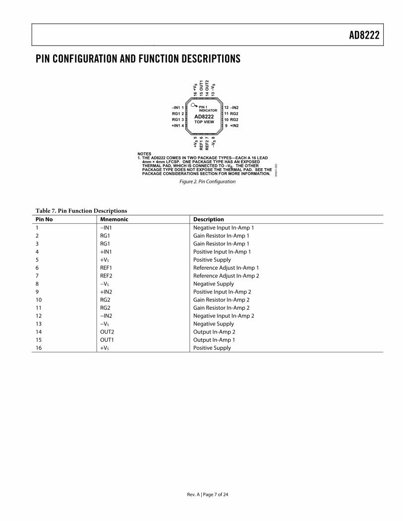
PIN CONFIGURATION AND FUNCTION DESCRIPTIONS
059
47-0
02
12
11
10
9
–IN1 1
RG1 2
RG1 3
+V
S5
RE
F1
6
RE
F2
7
–VS
8
+IN1 4
16 15 14 13
PIN 1INDICATOR
TOP VIEWAD8222
–IN2
RG2
RG2
+IN2
+V
S
OU
T1
OU
T2
–VS
NOTES1. THE AD8222 COMES IN TWO PACKAGE TYPES—EACH A 16 LEAD
4mm × 4mm LFCSP. ONE PACKAGE TYPE HAS AN EXPOSEDTHERMAL PAD, WHICH IS CONNECTED TO –VS. THE OTHERPACKAGE TYPE DOES NOT EXPOSE THE THERMAL PAD. SEE THEPACKAGE CONSIDERATIONS SECTION FOR MORE INFORMATION.
Figure 2. Pin Configuration
Table 7. Pin Function Descriptions Pin No Mnemonic Description 1 −IN1 Negative Input In-Amp 1 2 RG1 Gain Resistor In-Amp 1 3 RG1 Gain Resistor In-Amp 1 4 +IN1 Positive Input In-Amp 1 5 +VS Positive Supply 6 REF1 Reference Adjust In-Amp 1 7 REF2 Reference Adjust In-Amp 2 8 −VS Negative Supply 9 +IN2 Positive Input In-Amp 2 10 RG2 Gain Resistor In-Amp 2 11 RG2 Gain Resistor In-Amp 2 12 −IN2 Negative Input In-Amp 2 13 −VS Negative Supply 14 OUT2 Output In-Amp 2 15 OUT1 Output In-Amp 1 16 +VS Positive Supply
AD8222
Rev. A | Page 8 of 24
TYPICAL PERFORMANCE CHARACTERISTICS
500
400
300
200
100
0–50 50403020100–10–20–30–40
NU
MB
ER
OF
UN
ITS
CMRR (µV/V)0
5947
-003
N = 1713
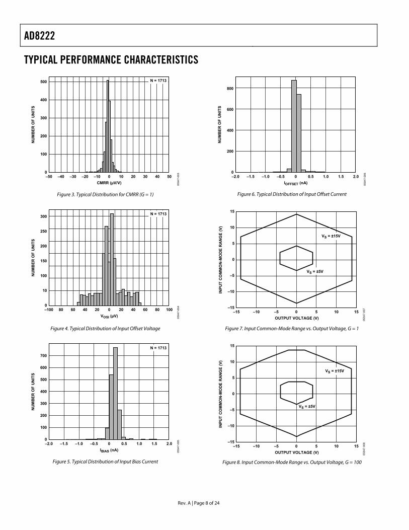
Figure 3. Typical Distribution for CMRR (G = 1)
300
250
200
150
100
10
0–100 10080604020020406080
NU
MB
ER
OF
UN
ITS
VOSI (µV)
059
47-0
04
N = 1713
Figure 4. Typical Distribution of Input Offset Voltage
700
600
500
400
300
200
100
0–2.0 2.01.51.00.50–0.5–1.0–1.5
NU
MB
ER
OF
UN
ITS
IBIAS (nA)
059
47-0
05
N = 1713
Figure 5. Typical Distribution of Input Bias Current
800
600
400
200
0–2.0 2.01.51.00.50–0.5–1.0–1.5
NU
MB
ER
OF
UN
ITS
IOFFSET (nA)
059
47-0
06
Figure 6. Typical Distribution of Input Offset Current
15
–15
–10
–5
0
5
10
–15 –10 –5 0 5 10 15
OUTPUT VOLTAGE (V)
059
47-0
07
INP
UT
CO
MM
ON
-MO
DE
RA
NG
E (
V)
VS = ±5V
VS = ±15V
Figure 7. Input Common-Mode Range vs. Output Voltage, G = 1
15
–15
–10
–5
0
5
10
–15 –10 –5 0 5 10 15
OUTPUT VOLTAGE (V)
059
47-0
08
INP
UT
CO
MM
ON
-MO
DE
RA
NG
E (
V)
VS = ±5V
VS = ±15V
Figure 8. Input Common-Mode Range vs. Output Voltage, G = 100
AD8222
Rev. A | Page 9 of 24
200
150
100
50
0
–50
–100
–150
–200–15 151050–5–10
INP
UT
BIA
S C
UR
RE
NT
(p
A)
COMMON-MODE VOLTAGE (V)
059
47-0
09
VS = ±15V
VS = ±5V
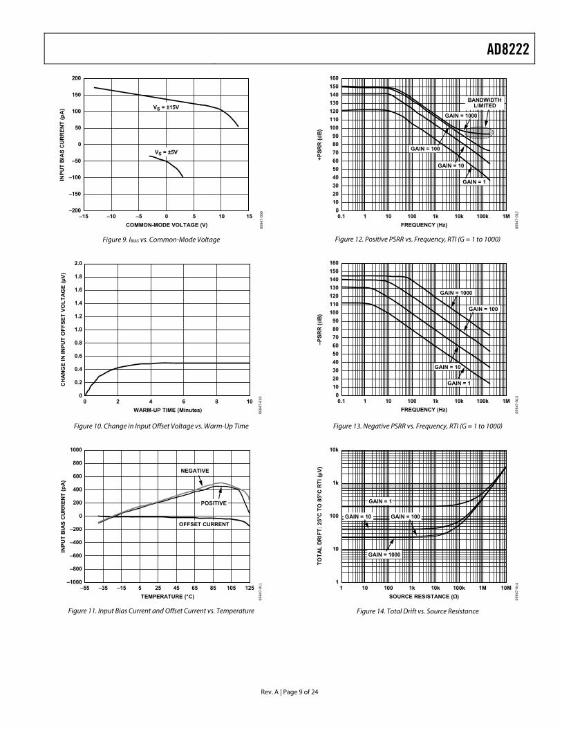
Figure 9. IBIAS vs. Common-Mode Voltage
2.0
0
0.2
0.4
0.6
0.8
1.0
1.2
1.4
1.6
1.8
0 2 4 6 8 10
WARM-UP TIME (Minutes)
059
47-0
10
CH
AN
GE
IN
IN
PU
T O
FF
SE
T V
OL
TA
GE
(µ
V)
Figure 10. Change in Input Offset Voltage vs. Warm-Up Time
1000
800
600
400
200
0
–200
–400
–600
–800
–1000–55 –35 –15 5 25 45 65 85 105 125
TEMPERATURE (°C)
059
47-0
11
INP
UT
BIA
S C
UR
RE
NT
(p
A)
POSITIVE
OFFSET CURRENT
NEGATIVE
Figure 11. Input Bias Current and Offset Current vs. Temperature
160
150
140
130
120
110
100
90
80
70
60
50
40
30
20
10
00.1 1M100k10k1k100101
FREQUENCY (Hz)
059
47-0
12
+P
SR
R (
dB
)
GAIN = 1
GAIN = 10
GAIN = 100
GAIN = 1000
BANDWIDTHLIMITED
Figure 12. Positive PSRR vs. Frequency, RTI (G = 1 to 1000)
160
150
140
130
120
110
100
90
80
70
60
50
40
30
20
10
00.1 1M100k10k1k100101
FREQUENCY (Hz)
059
47-0
13
–PS
RR
(d
B)
GAIN = 1
GAIN = 10
GAIN = 100
GAIN = 1000
Figure 13. Negative PSRR vs. Frequency, RTI (G = 1 to 1000)
10k
1k
100
10
11 10M1M100k10k1k10010
SOURCE RESISTANCE (Ω)
059
47-0
14
TO
TA
L D
RIF
T:
25°C
TO
85°
C R
TI
(µV
)
GAIN = 1
GAIN = 10 GAIN = 100
GAIN = 1000
Figure 14. Total Drift vs. Source Resistance
AD8222
Rev. A | Page 10 of 24
70
–40
–30
–20
–10
0
10
20
30
40
50
60
100 1k 10k 100k 1M 10M
GA
IN (
dB
)
FREQUENCY (Hz)
GAIN = 1
GAIN = 10
GAIN = 100
GAIN = 1000
059
47-0
15
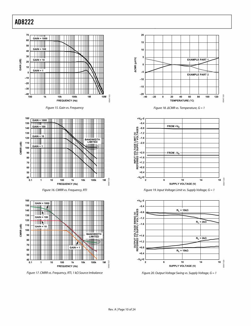
Figure 15. Gain vs. Frequency
160
150
140
130
120
110
100
90
80
70
60
50
400.1 1M100k10k1k100101
FREQUENCY (Hz)
059
47-0
16
CM
RR
(d
B)
GAIN = 1
GAIN = 10
GAIN = 100
GAIN = 1000
BANDWIDTHLIMITED
Figure 16. CMRR vs. Frequency, RTI
160
150
140
130
120
110
100
90
80
70
60
50
400.1 1M100k10k1k100101
FREQUENCY (Hz)
059
47-0
17
CM
RR
(d
B)
GAIN = 1000
GAIN = 100
GAIN = 10
GAIN = 1
BANDWIDTHLIMITED
Figure 17. CMRR vs. Frequency, RTI, 1 kΩ Source Imbalance
20
15
10
5
0
–5
–10
–15
–20–40 120100806040200–20
TEMPERATURE (°C)
059
47-0
18
ΔC
MR
(µ
V/V
)
EXAMPLE PART 1
EXAMPLE PART 2
Figure 18. ΔCMR vs. Temperature, G = 1
–VS+0
+0.4
+0.8
+1.2
+1.6
+2.0
FROM +VS
2 6 10 14 18
INP
UT
VO
LT
AG
E L
IMIT
(V
)R
EF
ER
RE
D T
O S
UP
PL
Y V
OL
TA
GE
S
SUPPLY VOLTAGE (V)
–2.0
–1.6
–1.2
–0.8
–0.4
+VS–0
FROM –VS
059
47-0
19
Figure 19. Input Voltage Limit vs. Supply Voltage, G = 1
OU
TP
UT
VO
LT
AG
E S
WIN
G (
V)
RE
FE
RR
ED
TO
SU
PP
LY
VO
LT
AG
ES
RL = 2kΩ
RL = 10kΩ
–1.6
–1.2
–0.4
+VS–0
–0.8
RL = 10kΩ
RL = 2kΩ
+0.4
–VS+0
+0.8
+1.2
+1.6
2 6 10 14 18
SUPPLY VOLTAGE (V)
059
47-0
20
Figure 20. Output Voltage Swing vs. Supply Voltage, G = 1
AD8222
Rev. A | Page 11 of 24
30
0
10
20
1 10 100 1k 10k
OU
TP
UT
VO
LT
AG
E S
WIN
G (
V p
-p)
LOAD RESISTANCE (Ω)
059
47-0
21
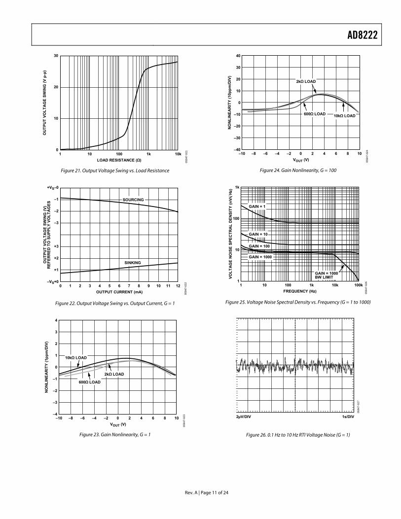
Figure 21. Output Voltage Swing vs. Load Resistance
OU
TP
UT
VO
LT
AG
E S
WIN
G (
V)
RE
FE
RR
ED
TO
SU
PP
LY
VO
LT
AG
ES
+VS–0
–1
–2
–3
+3
+2
+1
–VS+00 121110987654321
OUTPUT CURRENT (mA)
059
47-0
22
SINKING
SOURCING
Figure 22. Output Voltage Swing vs. Output Current, G = 1
–10 –8 –6 –4 –2 0 2 4 6 8 10
VOUT (V)
059
47-0
23
NO
NL
INE
AR
ITY
(1p
pm
/DIV
)
2kΩ LOAD
600Ω LOAD
10kΩ LOAD
4
3
2
1
0
–1
–2
–3
–4
Figure 23. Gain Nonlinearity, G = 1
–10 –8 –6 –4 –2 0 2 4 6 8 10
VOUT (V)
059
47-0
24
NO
NL
INE
AR
ITY
(10
pp
m/D
IV)
2kΩ LOAD
600Ω LOAD 10kΩ LOAD
40
30
20
10
0
–10
–20
–30
–40
Figure 24. Gain Nonlinearity, G = 100
1 101
10
100
1k
100 1k 10k 100k
FREQUENCY (Hz)
059
47-0
26
VO
LT
AG
E N
OIS
E S
PE
CT
RA
L D
EN
SIT
Y (
nV
/ H
z)
GAIN = 1
GAIN = 10
GAIN = 100
GAIN = 1000
GAIN = 1000BW LIMIT
Figure 25. Voltage Noise Spectral Density vs. Frequency (G = 1 to 1000)
059
47-0
27
2µV/DIV 1s/DIV
Figure 26. 0.1 Hz to 10 Hz RTI Voltage Noise (G = 1)

AD8222
Rev. A | Page 12 of 24
059
47-0
28
0.1µV/DIV 1s/DIV
Figure 27. 0.1 Hz to 10 Hz RTI Voltage Noise (G = 1000)
1 10 100 1k 10k 100k
FREQUENCY (Hz)
059
47-0
29
1k
100
10
CU
RR
EN
T N
OIS
E S
PE
CT
RA
L D
EN
SIT
Y (
fA/
Hz)
Figure 28. Current Noise Spectral Density vs. Frequency
059
47-0
30
5pA/DIV 1s/DIV
Figure 29. 0.1 Hz to 10 Hz Current Noise
1k 10k 100k 1M
FREQUENCY (Hz)
059
47-0
31
30
25
20
15
10
5
0
MA
X O
UT
PU
T V
OL
TA
GE
(V
p-p
)
GAIN = 1
GAIN = 10, 100, 1000
Figure 30. Large Signal Frequency Response
5V/DIV
0.002%/DIV
20µs/DIV
059
47-0
32
7.4µs TO 0.01%8.3µs TO 0.001%
Figure 31. Large Signal Pulse Response and Settling Time (G = 1)
5V/DIV
4.8µs TO 0.01%6.6µs TO 0.001%
0.002%/DIV
20µs/DIV
059
47-0
33
Figure 32. Large Signal Pulse Response and Settling (G = 10)

AD8222
Rev. A | Page 13 of 24
5V/DIV
20µs/DIV
0.002%/DIV
059
47-0
34
9.2µs TO 0.01%16.2µs TO 0.001%
Figure 33. Large Signal Pulse Response and Settling Time (G = 100)
059
47-0
35
5V/DIV
0.002%/DIV
83µs TO 0.01%112µs TO 0.001%
200µs/DIV
Figure 34. Large Signal Pulse Response and Settling Time (G = 1000)
059
47-
036
4µs/DIV20mV/DIV
Figure 35. Small Signal Response, G = 1, RL = 2 kΩ, CL = 100 pF
0594
7-0
37
4µs/DIV20mV/DIV
Figure 36. Small Signal Response, G = 10, RL = 2 kΩ, CL = 100 pF
0594
7-0
38
10µs/DIV20mV/DIV
Figure 37. Small Signal Response, G = 100, RL = 2 kΩ, CL = 100 pF
059
47-
039
100µs/DIV20mV/DIV
Figure 38. Small Signal Response, G = 1000, RL = 2 kΩ, CL = 100 pF
AD8222
Rev. A | Page 14 of 24
15
10
5
00 5 10 15 20
SE
TT
LIN
G T
IME
(µ
s)
OUTPUT VOLTAGE STEP SIZE (V)
059
47-0
40
SETTLED TO 0.01%
SETTLED TO 0.001%
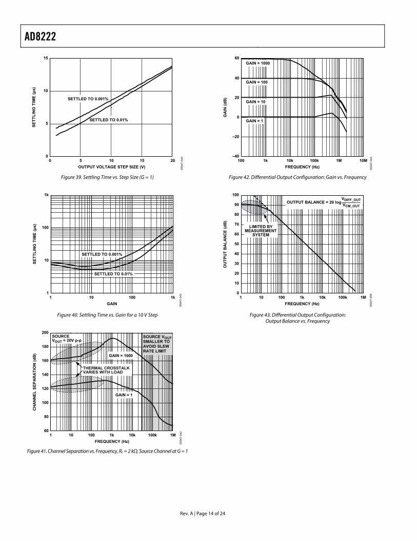
Figure 39. Settling Time vs. Step Size (G = 1)
1 10 100
SETTLED TO 0.01%
SETTLED TO 0.001%
1k
GAIN
059
47-0
41
1k
10
100
1
SE
TT
LIN
G T
IME
(µ
s)
Figure 40. Settling Time vs. Gain for a 10 V Step
200
180
160
140
120
100
80
601 1M100k10k1k10010
FREQUENCY (Hz)
059
47-0
42
CH
AN
NE
L S
EP
AR
AT
ION
(d
B)
GAIN = 1
GAIN = 1000
SOURCE VOUTSMALLER TOAVOID SLEWRATE LIMIT
SOURCEVOUT = 20V p-p
THERMAL CROSSTALKVARIES WITH LOAD
Figure 41. Channel Separation vs. Frequency, RL = 2 kΩ, Source Channel at G = 1
100 10k1k 100k 1M 10M
FREQUENCY (Hz)
059
47-0
43
60
–40
–20
0
20
40
GA
IN (
dB
)
GAIN = 1000
GAIN = 100
GAIN = 10
GAIN = 1
Figure 42. Differential Output Configuration: Gain vs. Frequency
1 10k1k10010 100k 1M
FREQUENCY (Hz)
059
47-0
56
100
90
80
70
60
50
40
30
20
10
0
OU
TP
UT
BA
LA
NC
E (
dB
)LIMITED BY
MEASUREMENTSYSTEM
OUTPUT BALANCE = 20 logVDIFF_OUT
VCM_OUT
Figure 43. Differential Output Configuration: Output Balance vs. Frequency
AD8222
Rev. A | Page 15 of 24
THEORY OF OPERATION
C1 C2
+VS
+IN–IN
–VS
–VS
10kΩ
10kΩ
10kΩ
400Ω 400Ω
10kΩ REF
OUTPUT
IB COMPENSATIONIB COMPENSATION
+VS
–VS
+VS
–VS
+VS
VBI I
R1 24.7kΩ 24.7kΩ
RG
Q1
R2
Q2
–VS
+VS
–VS
+VS
A2A1
A3
0594
7-0
45
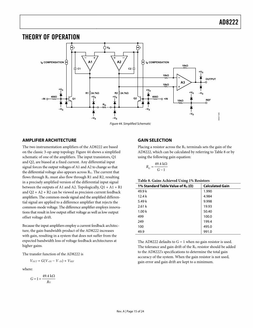
Figure 44. Simplified Schematic
AMPLIFIER ARCHITECTURE The two instrumentation amplifiers of the AD8222 are based on the classic 3-op-amp topology. Figure 44 shows a simplified schematic of one of the amplifiers. The input transistors, Q1 and Q2, are biased at a fixed current. Any differential input signal forces the output voltages of A1 and A2 to change so that the differential voltage also appears across RG. The current that flows through RG must also flow through R1 and R2, resulting in a precisely amplified version of the differential input signal between the outputs of A1 and A2. Topologically, Q1 + A1 + R1 and Q2 + A2 + R2 can be viewed as precision current feedback amplifiers. The common-mode signal and the amplified differen-tial signal are applied to a difference amplifier that rejects the common-mode voltage. The difference amplifier employs innova-tions that result in low output offset voltage as well as low output offset voltage drift.
Because the input amplifiers employ a current feedback architec-ture, the gain-bandwidth product of the AD8222 increases with gain, resulting in a system that does not suffer from the expected bandwidth loss of voltage feedback architectures at higher gains.
The transfer function of the AD8222 is
VOUT = G(V+IN − V−IN) + VREF
where:
GRG
kΩ49.41
GAIN SELECTION Placing a resistor across the RG terminals sets the gain of the AD8222, which can be calculated by referring to Table 8 or by using the following gain equation:
1kΩ49.4
G
RG
Table 8. Gains Achieved Using 1% Resistors 1% Standard Table Value of RG (Ω) Calculated Gain 49.9 k 1.990 12.4 k 4.984 5.49 k 9.998 2.61 k 19.93 1.00 k 50.40 499 100.0 249 199.4 100 495.0 49.9 991.0
The AD8222 defaults to G = 1 when no gain resistor is used. The tolerance and gain drift of the RG resistor should be added to the AD8222’s specifications to determine the total gain accuracy of the system. When the gain resistor is not used, gain error and gain drift are kept to a minimum.
AD8222
Rev. A | Page 16 of 24
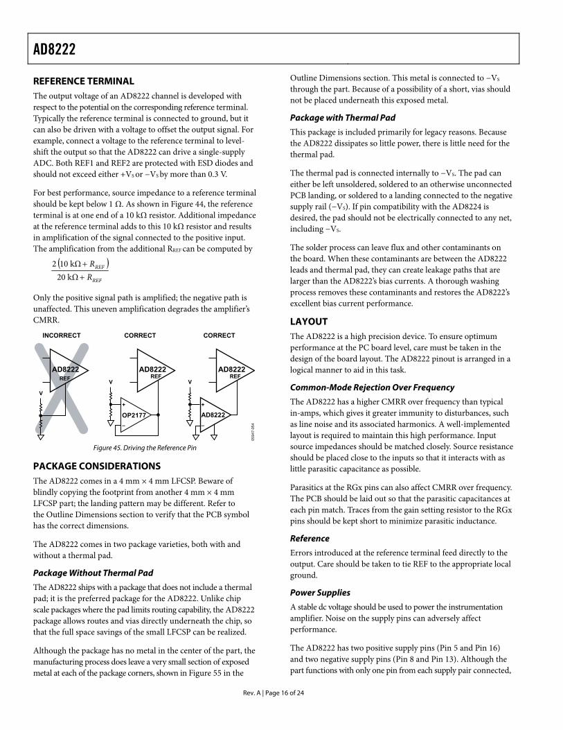
REFERENCE TERMINAL The output voltage of an AD8222 channel is developed with respect to the potential on the corresponding reference terminal. Typically the reference terminal is connected to ground, but it can also be driven with a voltage to offset the output signal. For example, connect a voltage to the reference terminal to level-shift the output so that the AD8222 can drive a single-supply ADC. Both REF1 and REF2 are protected with ESD diodes and should not exceed either +VS or −VS by more than 0.3 V.
For best performance, source impedance to a reference terminal should be kept below 1 Ω. As shown in Figure 44, the reference terminal is at one end of a 10 kΩ resistor. Additional impedance at the reference terminal adds to this 10 kΩ resistor and results in amplification of the signal connected to the positive input. The amplification from the additional RREF can be computed by
REF
REF
RR
kΩ20kΩ102
Only the positive signal path is amplified; the negative path is unaffected. This uneven amplification degrades the amplifier’s CMRR.
INCORRECT
AD8222
V
CORRECT
AD8222
OP2177
+
–
V
0594
7-05
4
CORRECT
AD8222
AD8222
+
–
VREF REF REF
Figure 45. Driving the Reference Pin
PACKAGE CONSIDERATIONS The AD8222 comes in a 4 mm × 4 mm LFCSP. Beware of blindly copying the footprint from another 4 mm × 4 mm LFCSP part; the landing pattern may be different. Refer to the Outline Dimensions section to verify that the PCB symbol has the correct dimensions.
The AD8222 comes in two package varieties, both with and without a thermal pad.
Package Without Thermal Pad
The AD8222 ships with a package that does not include a thermal pad; it is the preferred package for the AD8222. Unlike chip scale packages where the pad limits routing capability, the AD8222 package allows routes and vias directly underneath the chip, so that the full space savings of the small LFCSP can be realized.
Although the package has no metal in the center of the part, the manufacturing process does leave a very small section of exposed metal at each of the package corners, shown in Figure 55 in the
Outline Dimensions section. This metal is connected to −VS through the part. Because of a possibility of a short, vias should not be placed underneath this exposed metal.
Package with Thermal Pad
This package is included primarily for legacy reasons. Because the AD8222 dissipates so little power, there is little need for the thermal pad.
The thermal pad is connected internally to −VS. The pad can either be left unsoldered, soldered to an otherwise unconnected PCB landing, or soldered to a landing connected to the negative supply rail (−VS). If pin compatibility with the AD8224 is desired, the pad should not be electrically connected to any net, including −VS.
The solder process can leave flux and other contaminants on the board. When these contaminants are between the AD8222 leads and thermal pad, they can create leakage paths that are larger than the AD8222’s bias currents. A thorough washing process removes these contaminants and restores the AD8222’s excellent bias current performance.
LAYOUT The AD8222 is a high precision device. To ensure optimum performance at the PC board level, care must be taken in the design of the board layout. The AD8222 pinout is arranged in a logical manner to aid in this task.
Common-Mode Rejection Over Frequency
The AD8222 has a higher CMRR over frequency than typical in-amps, which gives it greater immunity to disturbances, such as line noise and its associated harmonics. A well-implemented layout is required to maintain this high performance. Input source impedances should be matched closely. Source resistance should be placed close to the inputs so that it interacts with as little parasitic capacitance as possible.
Parasitics at the RGx pins can also affect CMRR over frequency. The PCB should be laid out so that the parasitic capacitances at each pin match. Traces from the gain setting resistor to the RGx pins should be kept short to minimize parasitic inductance.
Reference
Errors introduced at the reference terminal feed directly to the output. Care should be taken to tie REF to the appropriate local ground.
Power Supplies
A stable dc voltage should be used to power the instrumentation amplifier. Noise on the supply pins can adversely affect performance.
The AD8222 has two positive supply pins (Pin 5 and Pin 16) and two negative supply pins (Pin 8 and Pin 13). Although the part functions with only one pin from each supply pair connected,
AD8222
Rev. A | Page 17 of 24
both pins should be connected for specified performance and optimum reliability.
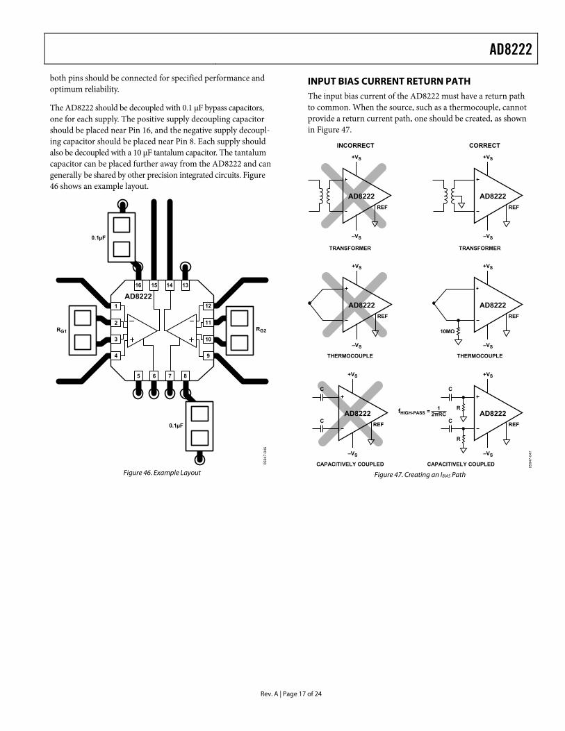
The AD8222 should be decoupled with 0.1 μF bypass capacitors, one for each supply. The positive supply decoupling capacitor should be placed near Pin 16, and the negative supply decoupl-ing capacitor should be placed near Pin 8. Each supply should also be decoupled with a 10 μF tantalum capacitor. The tantalum capacitor can be placed further away from the AD8222 and can generally be shared by other precision integrated circuits. Figure 46 shows an example layout.
059
47-0
46
AD82221
2
3
4
12
11
9
5 6 7 8
13141516
0.1µF
0.1µF
RG1 RG2
10
Figure 46. Example Layout
INPUT BIAS CURRENT RETURN PATH The input bias current of the AD8222 must have a return path to common. When the source, such as a thermocouple, cannot provide a return current path, one should be created, as shown in Figure 47.
THERMOCOUPLE
+VS
REF
–VS
AD8222
CAPACITIVELY COUPLED
+VS
REF
C
C
–VS
AD8222
TRANSFORMER
+VS
REF
–VS
AD8222
INCORRECT
CAPACITIVELY COUPLED
+VS
REF
C
R
R
C
–VS
AD82221fHIGH-PASS = 2πRC
THERMOCOUPLE
+VS
REF
–VS
10MΩ
AD8222
TRANSFORMER
+VS
REF
–VS
AD8222
CORRECT
0594
7-0
47
Figure 47. Creating an IBIAS Path
AD8222
Rev. A | Page 18 of 24
INPUT PROTECTION All terminals of the AD8222 are protected against ESD (1 kV, human body model). In addition, the input structure allows for dc overload conditions of about 2.5 V beyond the supplies.
Input Voltages Beyond the Rails
For larger input voltages, an external resistor should be used in series with each input to limit current during overload conditions. The AD8222 can safely handle a continuous 6 mA current. The limiting resistor can be computed from
Ω400mA6
SUPPLYINLIMIT
VVR
For applications in which the AD8222 encounters extreme over-load voltages, such as cardiac defibrillators, external series resistors and low leakage diode clamps, such as the BAV199L, the FJH1100, or the SP720, should be used.
Differential Input Voltages at High Gains
When operating at high gain, large differential input voltages can cause more than 6 mA of current to flow into the inputs. This condition occurs when the differential voltage exceeds the following critical voltage:
VCRITICAL = (400 + RG) × (6 mA)
This is true for differential voltages of either polarity.
The maximum allowed differential voltage can be increased by adding an input protection resistor in series with each input. The value of each protection resistor should be
RPROTECT = (VDIFF_MAX − VCRITICAL)/6 mA
RF INTERFERENCE RF rectification is often a problem when amplifiers are used in applications where there are strong RF signals. The disturbance can appear as a small dc offset voltage. High frequency signals can be filtered with a low-pass, RC network placed at the input of the instrumentation amplifier, as shown in Figure 48. The filter limits the input signal bandwidth according to the following relationship:
)(221
CDDiff
CCRFilterFreq
C
CMCR
FilterFreq
2
1
where CD ≥ 10CC.
R
R
AD8222
+15V
+IN
–IN
0.1µF 10µF
10µF0.1µF
REF
VOUT
–15V
R1499Ω
CD10nF
CC1nF
CC1nF
4.02kΩ
4.02kΩ
0594
7-04
8
Figure 48. RFI Suppression
Figure 48 shows an example where the differential filter fre-quency is approximately 2 kHz, and the common-mode filter frequency is approximately 40 kHz.
Values of R and CC should be chosen to minimize RFI. Mismatch between the R × CC at the positive input and the R × CC at negative input degrades the CMRR of the AD8222. By using a value of CD 10× larger than the value of CC, the effect of the mismatch is reduced and performance is improved.
COMMON-MODE INPUT VOLTAGE RANGE The 3-op-amp architecture of the AD8222 applies gain and then removes the common-mode voltage. Therefore, internal nodes in the AD8222 experience a combination of both the gained signal and the common-mode signal. This combined signal can be limited by the voltage supplies even when the individual input and output signals are not. Figure 7 and Figure 8 show the allowable common-mode input voltage ranges for various output voltages, supply voltages, and gains.

AD8222
Rev. A | Page 19 of 24
APPLICATIONS INFORMATION DIFFERENTIAL OUTPUT The differential configuration of the AD8222 has the same excellent dc precision specifications as the single-ended output configuration and is recommended for applications in the frequency range of dc to 100 kHz.
The circuit configuration is shown in Figure 49. The differential output specifications in Table 2 and Table 4 refer to this configura-tion only. The circuit includes an RC filter that maintains the stability of the loop.
The transfer function for the differential output is:
VDIFF_OUT = V+OUT − V−OUT = (V+IN − V−IN) × G
where GR
GkΩ49.4
1
+IN
–IN
+
–
+
–
AD8222
AD8222
+OUT
100pF
–OUT
+IN2
REF2
059
47-0
49
10kΩ
RG
Figure 49. Differential Circuit Schematic
Setting the Common-Mode Voltage
The output common-mode voltage is set by the average of +IN2 and REF2. The transfer function is
VCM_OUT = (V+OUT + V−OUT)/2 = (V+IN2 + VREF2)/2
+IN2 and REF2 have different properties that allow the reference voltage to be easily set for a wide variety of applications. +IN2 has high impedance but cannot swing to the supply rails of the part. REF2 must be driven with a low impedance but can go 300 mV beyond the supply rails.
A common application sets the common-mode output voltage to the midscale of a differential ADC. In this case, the ADC reference voltage is sent to the +IN2 terminal, and ground is connected to the REF2 terminal. This produces a common-mode output voltage of half the ADC reference voltage.
2-Channel Differential Output Using a Dual Op Amp
Another differential output topology is shown in Figure 50. Instead of a second in-amp, ½ of a dual OP2177 op amp creates the inverted output. Because the OP2177 is packaged in an MSOP, this configuration allows the creation of a dual channel, precision differential output in-amp with little board area.
Errors from the op amp are common to both outputs and are thus common mode. Errors from mismatched resistors also create a common-mode dc offset. Because these errors are common mode, they will likely be rejected by the next device in the signal chain.
+IN
–IN
REF
AD8222
VREF4.99kΩ
+–OP2177
+OUT
–OUT 0594
7-0
534.99kΩ
Figure 50. Differential Output Using Op Amp
AD8222
Rev. A | Page 20 of 24
AD8222(DIFF OUT)
100pFNPO
5%
100pFNPO
5%
1000pF
–IN
+IN
0.1µF10µF
0.1µF10µF
–12V
+12V
1kΩ
1kΩ
+
+
IN+VDD
GND REF
10µFX5R
AD7688IN–
0.1µF
+5V
ADR435GND
VINVOUT
0.1µF
+12V
0.1µF
+5V REF
059
47-0
51
+IN2REF2
+5V REF
+OUT
–OUT
1kΩ
2200pF 2200pF
1kΩ
Figure 51. Driving a Differential ADC
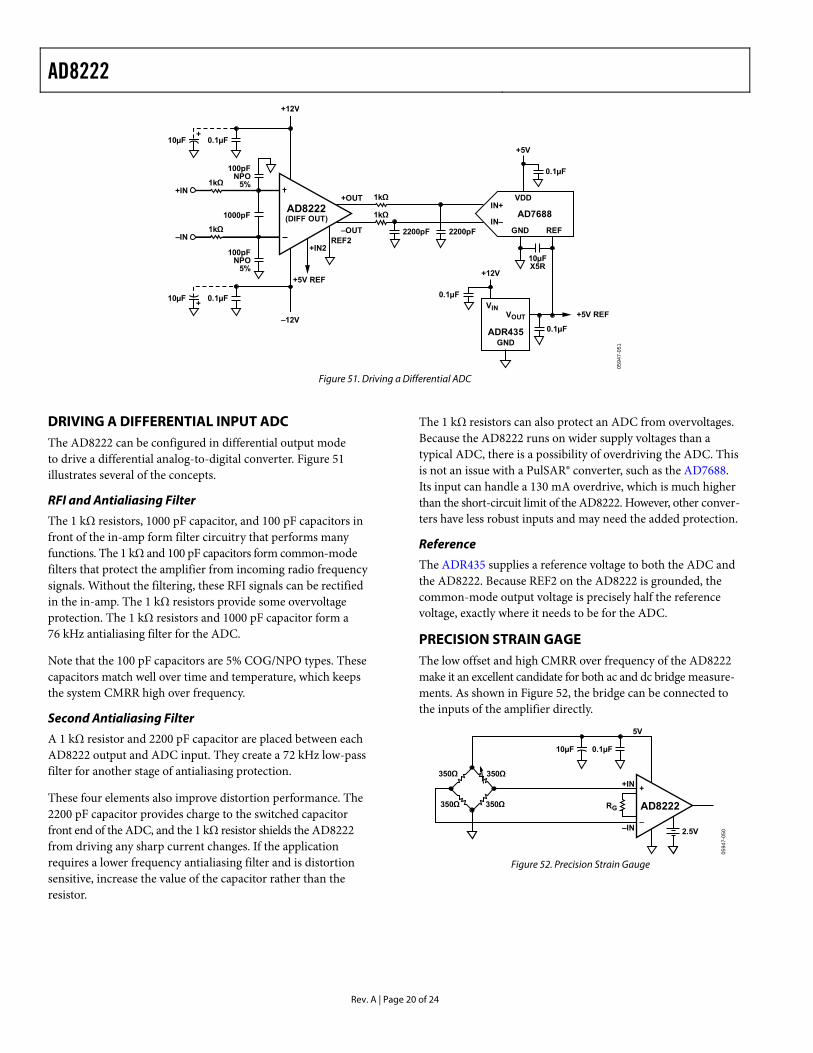
DRIVING A DIFFERENTIAL INPUT ADC The AD8222 can be configured in differential output mode to drive a differential analog-to-digital converter. Figure 51 illustrates several of the concepts.
RFI and Antialiasing Filter
The 1 kΩ resistors, 1000 pF capacitor, and 100 pF capacitors in front of the in-amp form filter circuitry that performs many functions. The 1 kΩ and 100 pF capacitors form common-mode filters that protect the amplifier from incoming radio frequency signals. Without the filtering, these RFI signals can be rectified in the in-amp. The 1 kΩ resistors provide some overvoltage protection. The 1 kΩ resistors and 1000 pF capacitor form a 76 kHz antialiasing filter for the ADC.
Note that the 100 pF capacitors are 5% COG/NPO types. These capacitors match well over time and temperature, which keeps the system CMRR high over frequency.
Second Antialiasing Filter
A 1 kΩ resistor and 2200 pF capacitor are placed between each AD8222 output and ADC input. They create a 72 kHz low-pass filter for another stage of antialiasing protection.
These four elements also improve distortion performance. The 2200 pF capacitor provides charge to the switched capacitor front end of the ADC, and the 1 kΩ resistor shields the AD8222 from driving any sharp current changes. If the application requires a lower frequency antialiasing filter and is distortion sensitive, increase the value of the capacitor rather than the resistor.
The 1 kΩ resistors can also protect an ADC from overvoltages. Because the AD8222 runs on wider supply voltages than a typical ADC, there is a possibility of overdriving the ADC. This is not an issue with a PulSAR® converter, such as the AD7688. Its input can handle a 130 mA overdrive, which is much higher than the short-circuit limit of the AD8222. However, other conver-ters have less robust inputs and may need the added protection.
Reference
The ADR435 supplies a reference voltage to both the ADC and the AD8222. Because REF2 on the AD8222 is grounded, the common-mode output voltage is precisely half the reference voltage, exactly where it needs to be for the ADC.
PRECISION STRAIN GAGE The low offset and high CMRR over frequency of the AD8222 make it an excellent candidate for both ac and dc bridge measure-ments. As shown in Figure 52, the bridge can be connected to the inputs of the amplifier directly.
5V
2.5V
10µF 0.1µF
AD8222
+IN
–IN
RG
350Ω
350Ω350Ω
350Ω
+
–
0594
7-05
0
Figure 52. Precision Strain Gauge
AD8222
Rev. A | Page 21 of 24
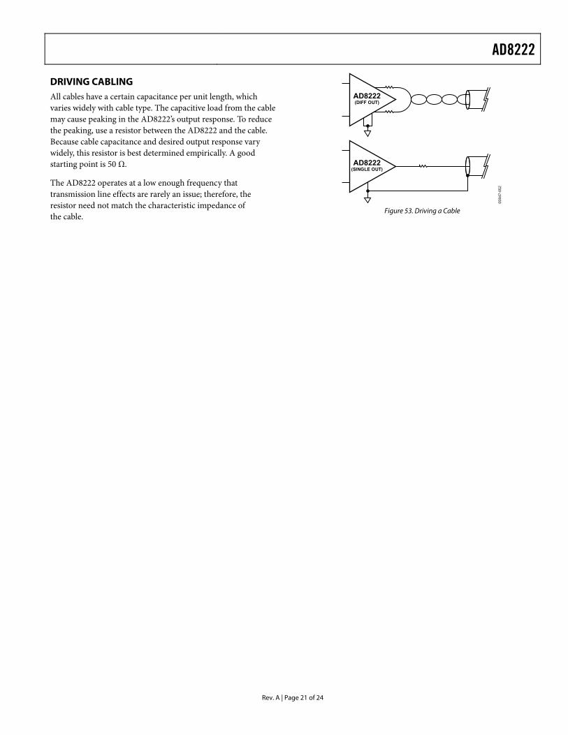
DRIVING CABLING All cables have a certain capacitance per unit length, which varies widely with cable type. The capacitive load from the cable may cause peaking in the AD8222’s output response. To reduce the peaking, use a resistor between the AD8222 and the cable. Because cable capacitance and desired output response vary widely, this resistor is best determined empirically. A good starting point is 50 Ω.
The AD8222 operates at a low enough frequency that transmission line effects are rarely an issue; therefore, the resistor need not match the characteristic impedance of the cable.
059
47-0
52
AD8222(DIFF OUT)
AD8222(SINGLE OUT)
Figure 53. Driving a Cable
AD8222
Rev. A | Page 22 of 24
OUTLINE DIMENSIONS
COMPLIANT TO JEDEC STANDARDS MO-220-VGGC.
1
0.65BSC
0.60 MAX PIN 1INDICATOR
1.95 BCS
0.500.400.30
0.25 MIN
3.75BSC SQ
TOP VIEW
12° MAX 0.80 MAX0.65 TYP
SEATINGPLANE
PIN 1INDICATOR
COPLANARITY0.08
1.000.850.80
0.300.230.18
0.05 MAX0.02 NOM
0.20 REF
4.00 BSC SQ
2.652.50 SQ2.35
16
5
13
89
12
4
EXPOSEDPAD
BOTTOM VIEW
031
006
-A
FOR PROPER CONNECTION OFTHE EXPOSED PAD, REFER TOTHE PIN CONFIGURATION ANDFUNCTION DESCRIPTIONSSECTION OF THIS DATA SHEET.
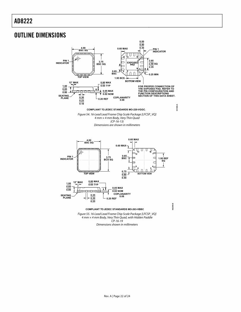
Figure 54. 16-Lead Lead Frame Chip Scale Package [LFCSP_VQ]
4 mm × 4 mm Body, Very Thin Quad (CP-16-13)
Dimensions are shown in millimeters
COMPLIANT TO JEDEC STANDARDS MO-263-VBBC 0623
09-B
3.75BCS SQ
4.00BSC SQ
0.65BSC
0.750.600.50
TOP VIEW
12° MAX 0.80 MAX0.65 TYP
SEATINGPLANE
PIN 1INDICATOR
COPLANARITY0.08
1.000.850.80
0.350.300.25
0.05 MAX0.02 NOM
0.20 REF
BOTTOM VIEW
0.60 MAX
0.60 MAX
1.95 REFSQ
116
589
1213
4
Figure 55. 16-Lead Lead Frame Chip Scale Package [LFCSP_VQ]
4 mm × 4 mm Body, Very Thin Quad, with Hidden Paddle CP-16-19
Dimensions shown in millimeters
AD8222
Rev. A | Page 23 of 24
ORDERING GUIDE
Model1 Temperature Range Product Description Package Description
Package Option
AD8222ACPZ-R7 −40°C to +85°C Standard Grade with Thermal Pad 16-Lead Lead Frame Chip Scale Package [LFCSP_VQ], 7“ Tape and Reel
CP-16-13
AD8222ACPZ-RL −40°C to +85°C Standard Grade with Thermal Pad 16-Lead Lead Frame Chip Scale Package [LFCSP_VQ], 13“Tape and Reel
CP-16-13
AD8222ACPZ-WP −40°C to +85°C Standard Grade with Thermal Pad 16-Lead Lead Frame Chip Scale Package [LFCSP_VQ], Waffle Pack
CP-16-13
AD8222BCPZ-R7 −40°C to +85°C High Performance Grade with Thermal Pad 16-Lead Lead Frame Chip Scale Package [LFCSP_VQ], 7“ Tape and Reel
CP-16-13
AD8222BCPZ-RL −40°C to +85°C High Performance Grade with Thermal Pad 16-Lead Lead Frame Chip Scale Package [LFCSP_VQ], 13” Tape and Reel
CP-16-13
AD8222BCPZ-WP −40°C to +85°C High Performance Grade with Thermal Pad 16-Lead Lead Frame Chip Scale Package [LFCSP_VQ], Waffle Pack
CP-16-13
AD8222HACPZ-R7 −40°C to +85°C Standard Grade Without Thermal Pad 16-Lead Lead Frame Chip Scale Package [LFCSP_VQ], 7” Tape and Reel
CP-16-19
AD8222HACPZ-RL −40°C to +85°C Standard Grade Without Thermal Pad 16-Lead Lead Frame Chip Scale Package [LFCSP_VQ], 13” Tape and Reel
CP-16-19
AD8222HACPZ-WP −40°C to +85°C Standard Grade Without Thermal Pad 16-Lead Lead Frame Chip Scale Package [LFCSP_VQ], Waffle Pack
CP-16-19
AD8222HBCPZ-R7 −40°C to +85°C High Performance Grade Without Thermal Pad 16-Lead Lead Frame Chip Scale Package [LFCSP_VQ], 7” Tape and Reel
CP-16-19
AD8222HBCPZ-RL −40°C to +85°C High Performance Grade Without Thermal Pad 16-Lead Lead Frame Chip Scale Package [LFCSP_VQ], 13” Tape and Reel
CP-16-19
AD8222HBCPZ-WP −40°C to +85°C High Performance Grade Without Thermal Pad 16-Lead Lead Frame Chip Scale Package [LFCSP_VQ], Waffle Pack
CP-16-19
AD8222-EVALZ Evaluation Board 1 Z = RoHS Compliant Part.

AD8222
Rev. A | Page 24 of 24
NOTES
©2006–2010 Analog Devices, Inc. All rights reserved. Trademarks and registered trademarks are the property of their respective owners. D05947-0-2/10(A)