Ei502microprocessorsmicrtocontrollerspart4 8051 Microcontroller

FEATURESANALOG FEATURES
24 Bits No Missing Codes 22 Bits Effective Resolution at 10Hz
− Low Noise: 75nV PGA From 1 to 128 Precision On-Chip Voltage Reference 8 Differential/Single-Ended Channels On-Chip Offset/Gain Calibration Offset Drift: 0.1ppm/ °C Gain Drift: 0.5ppm/ °C On-Chip Temperature Sensor Burnout Sensor Detection Single-Cycle Conversion Selectable Buffer Input
DIGITAL FEATURESMicrocontroller Core
8051-Compatible High-Speed Core
− 4 Clocks per Instruction Cycle DC to 33MHz Single Instruction 121ns Dual Data Pointer
Memory
Up To 32kB Flash Memory Flash Memory Partitioning Endurance 1M Erase/Write Cycles,
100 Year Data Retention In-System Serially Programmable External Program/Data Memory (64kB) 1,280 Bytes Data SRAM Flash Memory Security 2kB Boot ROM Programmable Wait State Control
Peripheral Features
34 I/O Pins Additional 32-Bit Accumulator Three 16-Bit Timer/Counters System Timers Programmable Watchdog Timer Full-Duplex Dual USARTs Master/Slave SPI 16-Bit PWM Power Management Control Idle Mode Current < 1mA Stop Mode Current < 1 A Programmable Brownout Reset Programmable Low Voltage Detect 24 Interrupt Sources Two Hardware Breakpoints
GENERAL FEATURES
Pin-Compatible with MSC1211/12/13/14 Package: TQFP-64 Low Power: 4mW Industrial Temperature Range:
−40°C to +125°C Power Supply: 2.7V to 5.25V
APPLICATIONS Industrial Process Control Instrumentation Liquid/Gas Chromatography Blood Analysis Smart Transmitters Portable Instruments Weigh Scales Pressure Transducers Intelligent Sensors Portable Applications DAS Systems
MSC1210
SBAS203J − MARCH 2002 − REVISED JANUARY 2008
Precision Analog-to-Digital Converter (ADC)with 8051 Microcontroller and Flash Memory
! !
www.ti.com
Copyright 2002−2008, Texas Instruments Incorporated
Please be aware that an important notice concerning availability, standard warranty, and use in critical applications of Texas Instrumentssemiconductor products and disclaimers thereto appears at the end of this data sheet.
All trademarks are the property of their respective owners.
"#$%$&
SBAS203J − MARCH 2002 − REVISED JANUARY 2008
www.ti.com
2
PACKAGE/ORDERING INFORMATION (1)
PRODUCT FLASH MEMORY PACKAGE MARKING
MSC1210Y2 4k MSC1210Y2MSC1210Y2 4k MSC1210Y2
MSC1210Y3 8k MSC1210Y3MSC1210Y3 8k MSC1210Y3
MSC1210Y4 16k MSC1210Y4MSC1210Y4 16k MSC1210Y4
MSC1210Y5 32k MSC1210Y5MSC1210Y5 32k MSC1210Y5
(1) For the most current package and ordering information, see the Package Option Addendum at the end of this datasheet, or refer to our web site at www.ti.com.
This integrated circuit can be damaged by ESD. Texas Instruments recommends that all integrated circuits be handled with appropriateprecautions. Failure to observe proper handling and installation procedures can cause damage.
ESD damage can range from subtle performance degradation to complete device failure. Precision integrated circuits may be more susceptible todamage because very small parametric changes could cause the device not to meet its published specifications.
ABSOLUTE MAXIMUM RATINGS (1)
MSC1210Yx UNITS
Analog Inputs
Input currentMomentary 100 mA
Input currentContinuous 10 mA
Input voltage AGND − 0.3 to AVDD + 0.3 V
Power Supply
DVDD to DGND −0.3 to +6 V
AVDD to AGND −0.3 to +6 V
AGND to DGND −0.3 to +0.3 V
VREF to AGND −0.3 to AVDD + 0.3 V
Digital input voltage to DGND −0.3 to DVDD + 0.3 V
Digital output voltage to DGND −0.3 to DVDD + 0.3 V
Maximum junction temperature 150 °C
Operating temperature range −40 to +125 °C
Storage temperature range −65 to +150 °C
Package power dissipation (TJ Max − TAMBIENT)/JA W
Output current, all pins 200 mA
Output pin short-circuit 10 s
Junction to ambient (JA)High K (2s 2p) 62.9 °C/W
Thermal ResistanceJunction to ambient (JA)
Low K (1s) 78.2 °C/WThermal Resistance
Junction to case (JC) 13.8 °C/W
Digital Outputs
Output current Continuous 100 mA
I/O source/sink current 100 mA
Power pin maximum 300 mA
(1) Stresses above those listed under Absolute Maximum Ratings may cause permanent damage to the device. Exposure to absolute maximum conditions forextended periods may affect device reliability.
MSC1210YX FAMILY FEATURESFEATURES(1) MSC1210Y2(2) MSC1210Y3(2) MSC1210Y4(2) MSC1210Y5(2)
Flash Program Memory (Bytes) Up to 4k Up to 8k Up to 16k Up to 32k
Flash Data Memory (Bytes) Up to 4k Up to 8k Up to 16k Up to 32k
Internal Scratchpad RAM (Bytes) 256 256 256 256
Internal MOVX RAM (Bytes) 1024 1024 1024 1024
Externally Accessible Memory (Bytes) 64k Program, 64k Data 64k Program, 64k Data 64k Program, 64k Data 64k Program, 64k Data
(1) All peripheral features are the same on all devices; the flash memory size is the only difference.(2) The last digit of the part number (N) represents the onboard flash size = (2N)kBytes.
"#$%$&
SBAS203J − MARCH 2002 − REVISED JANUARY 2008
www.ti.com
3
ELECTRICAL CHARACTERISTICS: AV DD = 5V All specifications from TMIN to TMAX, DVDD = +2.7V to 5.25V, fMOD = 15.625kHz, PGA = 1, Buffer ON, fDATA = 10Hz, Bipolar, and VREF ≡ (REF IN+) − (REF IN−) = +2.5V,unless otherwise noted.
MSC1210Yx
PARAMETER CONDITIONS MIN TYP MAX UNITS
Analog Input (AIN0-AIN7, AINCOM)
Analog Input RangeBuffer OFF AGND − 0.1 AVDD + 0.1 V
Analog Input RangeBuffer ON AGND + 50mV AVDD − 1.5 V
Full-Scale Input Voltage Range (In+) − (In−) ±VREF/PGA V
Differential Input Impedance Buffer OFF 7/PGA(5) MΩ
Input Current Buffer ON 0.5 nA
Fast Settling Filter −3dB 0.469 • fDATA
Bandwidth Sinc2 Filter −3dB 0.318 • fDATABandwidth
Sinc3 Filter −3dB 0.262 • fDATA
Programmable Gain Amplifier User-Selectable Gain Range 1 128
Input Capacitance Buffer On 9 pF
Input Leakage Current Multiplexer channel OFF, T = +25°C 0.5 pA
Burnout Current Sources Buffer On 2 µA
Offset DAC
Offset DAC Range ±VREF/(2•PGA) V
Offset DAC Monotonicity 8 Bits
Offset DAC Gain Error ±1.5 % of Range
Offset DAC Gain Error Drift 1 ppm/°C
System Performance
Resolution 24 Bits
ENOB See Typical Characteristics
Output Noise See Typical Characteristics
No Missing Codes Sinc3 Filter, Decimation > 360 24 Bits
Integral Nonlinearity End Point Fit, Differential Input ±0.0015 % of FSR
Offset Error After Calibration 7.5 ppm of FS
Offset Drift(1) Before Calibration 0.1 ppm of FS/°C
Gain Error(2) After Calibration 0.002 %
Gain Error Drift(1) Before Calibration 0.5 ppm/°C
System Gain Calibration Range 80 120 % of FS
System Offset Calibration Range −50 50 % of FS
At DC 100 115 dB
ADC Common-Mode RejectionfCM = 60Hz, fDATA = 10Hz 130 dB
ADC Common-Mode RejectionfCM = 50Hz, fDATA = 50Hz 120 dB
fCM = 60Hz, fDATA = 60Hz 120 dB
Normal-Mode RejectionfSIG = 50Hz, fDATA = 50Hz 100 dB
Normal-Mode RejectionfSIG = 60Hz, fDATA = 60Hz 100 dB
Power-Supply Rejection At DC, dB = −20log(∆VOUT/∆VDD)(3) 80 88 dB
(1) Calibration can minimize these errors.(2) The self-gain calibration cannot have a REF IN+ of more than AVDD −1.5V with Buffer ON. To calibrate gain, turn Buffer OFF.(3) ∆VOUT is change in digital result.(4) 9pF switched capacitor at fSAMP clock frequency (see Figure 14).(5) The input impedance for PGA = 128 is the same as that for PGA = 64 (that is, 7MΩ/64).

"#$%$&
SBAS203J − MARCH 2002 − REVISED JANUARY 2008
www.ti.com
4
ELECTRICAL CHARACTERISTICS: AV DD = 5V (continued)All specifications from TMIN to TMAX, DVDD = +2.7V to 5.25V, fMOD = 15.625kHz, PGA = 1, Buffer ON, fDATA = 10Hz, Bipolar, and VREF ≡ (REF IN+) − (REF IN−) = +2.5V,unless otherwise noted.
MSC1210Yx
PARAMETER UNITSMAXTYPMINCONDITIONS
Voltage Reference Input
Reference Input Range REF IN+, REF IN− AGND AVDD(2) V
VREF VREF ≡ (REF IN+) − (REF IN−) 0.1 2.5 AVDD V
VREF Common-Mode RejectionAt DC 130 dB
VREF Common-Mode RejectionfCM = 60Hz, fDATA = 60Hz 120 dB
Input Current(4) VREF = 2.5V 3 µA
On-Chip Voltage Reference
Output VoltageVREFH = 1 at +25°C, ACLK = 1MHz 2.495 2.5 2.505 V
Output VoltageVREFH = 0 at +25°C, ACLK = 1MHz 1.25 V
Power-Supply Rejection Ratio 65 dB
Short-Circuit Current Source 8 mA
Short-Circuit Current Sink 50 µA
Short-Circuit Duration Sink or Source Indefinite
Drift 5 ppm/°C
Output Impedance Sourcing 100µA 3 Ω
Startup Time from Power On CREF = 0.1µF 8 ms
Temperature Sensor Voltage T = +25°C 115 mV
Temperature Sensor Coefficient 375 µV/°C
Analog Power-Supply Requirements
Analog Power-Supply Voltage AVDD 4.75 5.0 5.25 V
Analog Current(IADC + IVREF)
PDADC = 1, ALVDIS = 1, DAB = 1 < 1 nA
PGA = 1, Buffer OFF 200 µA
AnalogPower-Supply
ADC Current PGA = 128, Buffer OFF 500 µAPower-SupplyCurrent
ADC Current(IADC) PGA = 1, Buffer ON 240 µACurrent ADC
PGA = 128, Buffer ON 850 µA
VREF Supply Current(IVREF)
ADC ON, VREF = 2.5V 250 µA
(1) Calibration can minimize these errors.(2) The self-gain calibration cannot have a REF IN+ of more than AVDD −1.5V with Buffer ON. To calibrate gain, turn Buffer OFF.(3) ∆VOUT is change in digital result.(4) 9pF switched capacitor at fSAMP clock frequency (see Figure 14).(5) The input impedance for PGA = 128 is the same as that for PGA = 64 (that is, 7MΩ/64).

"#$%$&
SBAS203J − MARCH 2002 − REVISED JANUARY 2008
www.ti.com
5
ELECTRICAL CHARACTERISTICS: AV DD = 3V All specifications from TMIN to TMAX, DVDD = +2.7V to 5.25V, fMOD = 15.625kHz, PGA = 1, Buffer ON, fDATA = 10Hz, Bipolar, and VREF ≡ (REF IN+) − (REF IN−) = +1.25V,unless otherwise noted.
MSC1210Yx
PARAMETER CONDITIONS MIN TYP MAX UNITS
ANALOG INPUT (AIN0-AIN7, AINCOM)
Analog Input RangeBuffer OFF AGND − 0.1 AVDD + 0.1 V
Analog Input RangeBuffer ON AGND + 50mV AVDD − 1.5 V
Full-Scale Input Voltage Range (In+) − (In−) ±VREF/PGA V
Differential Input Impedance Buffer OFF 7/PGA(5) MΩ
Input Current Buffer ON 0.5 nA
Fast Settling Filter −3dB 0.469 • fDATA
Bandwidth Sinc2 Filter −3dB 0.318 • fDATABandwidth
Sinc3 Filter −3dB 0.262 • fDATA
Programmable Gain Amplifier User-Selectable Gain Range 1 128
Input Capacitance 9 pF
Input Leakage Current Multiplexer channel OFF, T = +25°C 0.5 pA
Burnout Current Sources Sensor Input Open Circuit 2 µA
OFFSET DAC
Offset DAC Range ±VREF/(2•PGA) V
Offset DAC Monotonicity 8 Bits
Offset DAC Gain Error ±1.5 % of Range
Offset DAC Gain Error Drift 1 ppm/°C
SYSTEM PERFORMANCE
Resolution 24 Bits
ENOB See Typical Characteristics
Output Noise See Typical Characteristics
No Missing Codes Sinc3 Filter 24 Bits
Integral Nonlinearity End Point Fit, Differential Input ±0.0015 % of FSR
Offset Error After Calibration 7.5 ppm of FS
Offset Drift(1) Before Calibration 0.1 ppm of FS/°C
Gain Error(2) After Calibration 0.005 %
Gain Error Drift(1) Before Calibration 0.5 ppm/°C
System Gain Calibration Range 80 120 % of FS
System Offset Calibration Range −50 50 % of FS
At DC 100 115 dB
ADC Common-Mode RejectionfCM = 60Hz, fDATA = 10Hz 130 dB
ADC Common-Mode RejectionfCM = 50Hz, fDATA = 50Hz 120 dB
fCM = 60Hz, fDATA = 60Hz 120 dB
Normal-Mode RejectionfSIG = 50Hz, fDATA = 50Hz 100 dB
Normal-Mode RejectionfSIG = 60Hz, fDATA = 60Hz 100 dB
Power-Supply Rejection At DC, dB = −20log(∆VOUT/∆VDD)(3) 85 dB
(1) Calibration can minimize these errors.(2) The self-gain calibration cannot have a REF IN+ of more than AVDD −1.5V with Buffer ON. To calibrate gain, turn Buffer OFF.(3) ∆VOUT is change in digital result.(4) 9pF switched capacitor at fSAMP clock frequency (see Figure 14).(5) The input impedance for PGA = 128 is the same as that for PGA = 64 (that is, 7MΩ/64).

"#$%$&
SBAS203J − MARCH 2002 − REVISED JANUARY 2008
www.ti.com
6
ELECTRICAL CHARACTERISTICS: AV DD = 3V (continued)All specifications from TMIN to TMAX, DVDD = +2.7V to 5.25V, fMOD = 15.625kHz, PGA = 1, Buffer ON, fDATA = 10Hz, Bipolar, and VREF ≡ (REF IN+) − (REF IN−) = +1.25V,unless otherwise noted.
MSC1210Yx
PARAMETER UNITSMAXTYPMINCONDITIONS
VOLTAGE REFERENCE INPUT
Reference Input Range REF IN+, REF IN− AGND AVDD(2) V
VREF VREF ≡ (REF IN+) − (REF IN−) 0.1 1.25 AVDD V
VREF Common-Mode RejectionAt DC 130 dB
VREF Common-Mode RejectionfCM = 60Hz, fDATA = 60Hz 120 dB
Input Current(4) VREF = 1.25V 1.5 µA
ON-CHIP VOLTAGE REFERENCE
Output Voltage VREFH = 0 at +25°C, ACLK = 1MHz 1.245 1.25 1.255 V
Power-Supply Rejection Ratio 65 dB
Short-Circuit Current Source 8 mA
Short-Circuit Current Sink 50 µA
Short-Circuit Duration Sink or Source Indefinite
Drift 5 ppm/°C
Output Impedance Sourcing 100µA 3 Ω
Startup Time from Power OFF CREF = 0.1µF 8 ms
Temperature Sensor Voltage T = +25°C 115 mV
Temperature Sensor Coefficient 375 µV/°C
ANALOG POWER-SUPPLY REQUIREMENTS
Analog Power-Supply Voltage AVDD 2.7 3.6 V
Analog Current(IADC + IVREF)
PDADC = 1, ALVDIS = 1, DAB = 1 < 1 nA
PGA = 1, Buffer OFF 200 µA
AnalogPower-Supply
ADC Current PGA = 128, Buffer OFF 500 µAPower-SupplyCurrent
ADC Current(IADC) PGA = 1, Buffer ON 240 µACurrent ADC
PGA = 128, Buffer ON 850 µA
VREF Supply Current(IVREF)
ADC ON, , VREF = 1.25V 240 µA
(1) Calibration can minimize these errors.(2) The self-gain calibration cannot have a REF IN+ of more than AVDD −1.5V with Buffer ON. To calibrate gain, turn Buffer OFF.(3) ∆VOUT is change in digital result.(4) 9pF switched capacitor at fSAMP clock frequency (see Figure 14).(5) The input impedance for PGA = 128 is the same as that for PGA = 64 (that is, 7MΩ/64).

"#$%$&
SBAS203J − MARCH 2002 − REVISED JANUARY 2008
www.ti.com
7
DIGITAL CHARACTERISTICS: DV DD = 2.7V to 5.25VAll specifications from TMIN to TMAX, fOSC = 1MHz, unless otherwise specified.
MSC1210Yx
PARAMETER CONDITIONS MIN TYP MAX UNITS
DIGITAL POWER-SUPPLY REQUIREMENTS
Digital Power-Supply Voltage DVDD 2.7 3.0 3.6 V
Normal Mode, fOSC = 1MHz 1.4 1.6 mA
Normal Mode, fOSC = 8MHz 8 9 mA
Stop Mode(1) 0.5 µA
Digital Power-Supply Current DVDD 4.75 5.0 5.25 VDigital Power-Supply Current
Normal Mode, fOSC = 1MHz 2 2.2 mA
Normal Mode, fOSC = 8MHz 17 18 mA
Stop Mode(1) 0.5 µA
DIGITAL INPUT/OUTPUT (CMOS)
Logic LevelVIH (except XIN pin) 0.6 • DVDD DVDD V
Logic LevelVIL (except XIN pin) DGND 0.2 • DVDD V
I/O Pin Hysteresis 700 mV
Ports 0−3, Input Leakage Current, Input Mode VIH = DVDD or VIH = 0V < 1 pA
Pins EA, XIN Input Leakage Current < 1 pA
VOL, ALE, PSEN, Ports 0−3, All Output ModesIOL = 1mA DGND 0.4 V
VOL, ALE, PSEN, Ports 0−3, All Output ModesIOL = 30mA 1.5 V
VOH, ALE, PSEN, Ports 0−3, Strong Drive OutputIOH = 1mA DVDD − 0.4 DVDD − 0.1 DVDD V
VOH, ALE, PSEN, Ports 0−3, Strong Drive OutputIOH = 30mA DVDD − 1.5 V
Ports 0−3, Pull-Up Resistors 9 kΩ
Pins ALE, PSEN, Pull-Up Resistors Flash Programming Mode Only 9 kΩ
Pin RST, Pull-Down Resistor 500 kΩ
(1) Digital Brownout Detect disabled (HCR1.2 = 1), Low Voltage Detect disabled (LVDCON.3 =1). Ports configured for CMOS output low. If in External Oscillation mode, theoscillator must be disabled.
FLASH MEMORY CHARACTERISTICS: DV DD = 2.7V to 5.25VMSC1210Yx
PARAMETER CONDITIONS MIN TYP MAX UNITS
Flash Memory Endurance 100,000 1,000,000 cycles
Flash Memory Data Retention 100 years
Mass and Page Erase Time Set with FER in FTCON 10 ms
Flash Memory Write Time Set with FWR in FTCON 30 40 µs
Flash Programming CurrentDVDD = 3.0V 10 mA
Flash Programming CurrentDVDD = 5.0V 25 mA

"#$%$&
SBAS203J − MARCH 2002 − REVISED JANUARY 2008
www.ti.com
8
AC ELECTRICAL CHARACTERISTICS (1)(2): DVDD = 2.7V to 5.25V2.7V to 3.6V 4.75V to 5.25V
SYMBOL FIGURE PARAMETER MIN MAX MIN MAX UNITS
System Clock
External Crystal Frequency (fOSC) 1 18 1 33 MHz
1/tCLK(4) 4 External Clock Frequency (fOSC) 0 18 0 33 MHz1/tCLK(4) 4External Ceramic Resonator Frequency (fOSC) 1 16 1 16 MHz
Program Memory
tLHLL 1 ALE Pulse Width 1.5tCLK − 5 1.5tCLK − 5 ns
tAVLL 1 Address Valid to ALE LOW 0.5tCLK − 10 0.5tCLK − 7 ns
tLLAX 1 Address Hold After ALE LOW 0.5tCLK 0.5tCLK ns
tLLIV 1 ALE LOW to Valid Instruction In 2.5tCLK − 35 2.5tCLK − 25 ns
tLLPL 1 ALE LOW to PSEN LOW 0.5tCLK 0.5tCLK ns
tPLPH 1 PSEN Pulse Width 2tCLK − 5 2tCLK − 5 ns
tPLIV 1 PSEN LOW to Valid Instruction in 2tCLK − 40 2tCLK − 30 ns
tPXIX 1 Input Instruction Hold After PSEN 5 −5 ns
tPXIZ 1 Input Instruction Float After PSEN tCLK − 5 tCLK ns
tAVIV 1 Address to Valid Instruction In 3tCLK − 40 3tCLK − 25 ns
tPLAZ 1 PSEN LOW to Address Float 0 0 ns
Data Memory
tRLRH 2RD Pulse Width (tMCS = 0)(5) 2tCLK − 5 2tCLK − 5 ns
tRLRH 2 RD Pulse Width (tMCS > 0)(5) tMCS − 5 tMCS − 5 ns
tWLWH 3WR Pulse Width (tMCS = 0)(5) 2tCLK − 5 2tCLK − 5 ns
tWLWH 3 WR Pulse Width (tMCS > 0)(5) tMCS − 5 tMCS − 5 ns
tRLDV 2RD LOW to Valid Data In (tMCS = 0)(5) 2tCLK − 40 2tCLK − 30 ns
tRLDV 2 RD LOW to Valid Data In (tMCS > 0)(5) tMCS − 40 tMCS − 30 ns
tRHDX 2 Data Hold After Read −5 −5 ns
tRHDZ 2Data Float After Read (tMCS = 0)(5) tCLK tCLK ns
tRHDZ 2 Data Float After Read (tMCS > 0)(5) 2tCLK 2tCLK ns
tLLDV 2ALE LOW to Valid Data In (tMCS = 0)(5) 2.5tCLK − 40 2.5tCLK − 25 ns
tLLDV 2 ALE LOW to Valid Data In (tMCS > 0)(5) tCLK + tMCS − 40 tCLK + tMCS − 25 ns
tAVDV 2Address to Valid Data In (tMCS = 0)(5) 3tCLK − 40 3tCLK − 25 ns
tAVDV 2 Address to Valid Data In (tMCS > 0)(5) 1.5tCLK + tMCS − 40 1.5tCLK + tMCS − 25 ns
tLLWL 2, 3ALE LOW to RD or WR LOW (tMCS = 0)(5) 0.5tCLK − 5 0.5tCLK + 5 0.5tCLK − 5 0.5tCLK + 5 ns
tLLWL 2, 3 ALE LOW to RD or WR LOW (tMCS > 0)(5) tCLK − 5 tCLK + 5 tCLK − 5 tCLK + 5 ns
tAVWL 2, 3Address to RD or WR LOW (tMCS = 0)(5) tCLK − 5 tCLK − 5 ns
tAVWL 2, 3 Address to RD or WR LOW (tMCS > 0)(5) 2tCLK − 5 2tCLK − 5 ns
tQVWX 3 Data Valid to WR Transition −8 −5 ns
tWHQX 3 Data Hold After WR tCLK − 8 tCLK − 5 ns
tRLAZ 2 RD LOW to Address Float −0.5tCLK − 5 −0.5tCLK − 5 ns
tWHLH 2, 3RD or WR HIGH to ALE HIGH (tMCS = 0)(5) −5 5 −5 5 ns
tWHLH 2, 3 RD or WR HIGH to ALE HIGH (tMCS > 0)(5) tCLK − 5 tCLK + 5 tCLK − 5 tCLK + 5 ns
External Clock
tHIGH 4 HIGH Time(3) 15 10 ns
tLOW 4 LOW Time(3) 15 10 ns
tR 4 Rise Time(3) 5 5 ns
tF 4 Fall Time(3) 5 5 ns
(1) Parameters are valid over operating temperature range, unless otherwise specified.(2) Load capacitance for Port 0, ALE, and PSEN = 100pF; load capacitance for all other outputs = 80pF.(3) These values are characterized but not 100% production tested.(4) In the MSC1210, fOSC = fCLK. tCLK = 1/fosc = one oscillator clock period.(5) tMCS is a time period related to the Stretch MOVX selection. The following table shows the value of tMCS for each stretch selection:
MD2 MD1 MD0 MOVX DURATION tMCS
0 0 0 2 Machine Cycles 0
0 0 1 3 Machine Cycles (default) 4tCLK
0 1 0 4 Machine Cycles 8tCLK
0 1 1 5 Machine Cycles 12tCLK
1 0 0 6 Machine Cycles 16tCLK
1 0 1 7 Machine Cycles 20tCLK
1 1 0 8 Machine Cycles 24tCLK
1 1 1 9 Machine Cycles 28tCLK

"#$%$&
SBAS203J − MARCH 2002 − REVISED JANUARY 2008
www.ti.com
9
EXPLANATION OF THE AC SYMBOLSEach Timing Symbol has five characters. The first character is always ‘t’ (= time). The other characters, depending on their positions, indicate the name of a signalor the logical status of that signal. The designators are:AAddress
CClock
DInput Data
HLogic Level HIGH
IInstruction (program memory contents)
LLogic Level LOW, or ALE
PPSEN
QOutput Data
RRD Signal
tTime
VValid
WWR Signal
XNo Longer a Valid Logic Level
ZFloat
Examples:
(1) tAVLL = Time for address valid to ALE LOW.
(2) tLLPL = Time for ALE LOW to PSEN LOW.
tLHLL
tAVLL tLLPLtPLPH
tLLIV
tLLAX tPLAZ
tPXIZ
tPXIX
tAVIV
tPLIV
A0−A7 A0−A7
A8−A15A8−A15
INSTR IN
ALE
PSEN
PORT 0
PORT 2
Figure 1. External Program Memory Read Cycle
tAVLL
ALE
RD
PSEN
PORT 0
PORT 2
A0−A7from RI or DPL DATA IN A0−A7from PCL INSTR IN
P2.0−P2.7 or A8−A15 from DPH A8−A15 from PCH
tAVDV
tLLDV
tWHLH
tRLRHtLLWL
tLLAX
tRLAZ tRHDX
tRLDV
tAVWL
tRHDZ
Figure 2. External Data Memory Read Cycle
"#$%$&
SBAS203J − MARCH 2002 − REVISED JANUARY 2008
www.ti.com
10
tWHLH
tAVLL
tLLWL
tWHQX
tLLAX
tAVWL
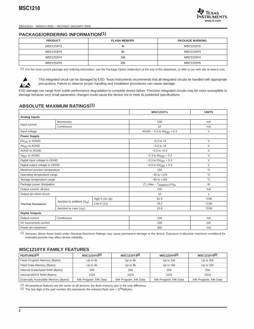
tWLWH
tDW
tQVWX
ALE
WR
PSEN
PORT 0
PORT 2
from RI or DPL DATA OUT from PCL INSTR IN
P2.0−P2.7or A8−A15 from DPH A8−A15 from PCH
A0−A7A0−A7
Figure 3. External Data Memory Write Cycle
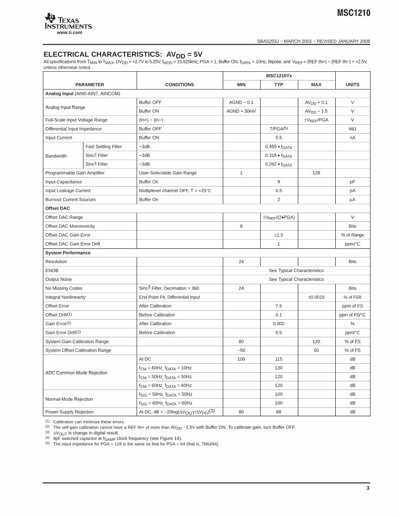
trtHIGH
VIH1 VIH1
0.8V 0.8V
VIH1 VIH1
0.8V 0.8VtLOW
t
tf
CLK
Figure 4. External Clock Drive CLK

"#$%$&
SBAS203J − MARCH 2002 − REVISED JANUARY 2008
www.ti.com
11
RESET AND POWER-ON TIMING
tRW
tRS tRH
tRFD
tRFD
RST
PSEN
ALE
NOTE: PSEN and ALE are internally pulled up with ~9kΩ during RST high.
EA
tRRD
tRRD
Figure 5. Reset Timing
tRFD
PSEN
ALE
NOTE: PSEN and ALE are internally pulled up with ~9kΩ during RST high.
tRW
RST
tRS tRH
tRRD
tRRD
Figure 6. Parallel Flash Programming Power-On Timing (EA is ignored)
tRFD
PSEN
ALE
NOTE: PSEN and ALE are internally pulled up with ~9kΩ during RST high.
tRW
RST
tRS tRHtRRD
tRRD
Figure 7. Serial Flash Programming Power-On Timing (EA is ignored)
SYMBOL PARAMETER MIN MAX UNIT
tRW RST width 2tOSC — ns
tRRD RST rise to PSEN ALE internal pull HIGH — 5 µs
tRFD RST falling to PSEN and ALE start — (217 + 512)tOSC ns
tRS Input signal to RST falling setup time tOSC — ns
tRH RST falling to input signal hold time (217 + 512)tOSC — ns

"#$%$&
SBAS203J − MARCH 2002 − REVISED JANUARY 2008
www.ti.com
12
PIN ASSIGNMENTS
PAG PACKAGETQFP-64
(TOP VIEW)
48
47
46
45
44
43
42
41
40
39
38
37
36
35
34
33
EA
P0.6/AD6
P0.7/AD7
ALE
PSEN/OSCCLK/MODCLK
P2.7/A15
DVDD
DGND
P2.6/A14
P2.5/A13
P2.4/A12
P2.3/A11
P2.2/A10
P2.1/A09
P2.0/A08
NC(1)
1
2
3
4
5
6
7
8
9
10
11
12
13
14
15
16
XOUT
XIN
P3.0/RxD0
P3.1/TxD0
P3.2/INT0
P3.3/INT1/TONE/PWM
P3.4/T0
P3.5/T1
P3.6/WR
P3.7/RD
DVDD
DGND
RST
DVDD
DVDD
NOTE: (1) NC pin must be left unconnected.
P1.
7/IN
T5
/SC
LK
P1.
6/IN
T4
/MIS
O
P1.
5/IN
T3
/MO
SI
P1.
4/IN
T2
/SS
P1.
3/T
xD1
P1.
2/R
xD1
DV
DD
DG
ND
P1.
1/T
2E
X
P1.
0/T
2
P0.
0/A
D0
P0.
1/A
D1
P0.
2/A
D2
P0.
3/A
D3
P0.
4/A
D4
P0.
5/A
D5
AG
ND
AIN
0
AIN
1
AIN
2
AIN
3
AIN
4
AIN
5
AIN
6/E
XT
D
AIN
7/E
XT
A
AIN
CO
M
AG
ND
AV
DD
RE
FIN
−
RE
FIN
+
RE
FO
UT
NC
(1)
64 63 62 61 60 59 58 57 56 55 54
17 18 19 20 21 22 23 24 25 26 27
53 52 51 50 49
28 29 30 31 32
MSC1210
NC(1)

"#$%$&
SBAS203J − MARCH 2002 − REVISED JANUARY 2008
www.ti.com
13
PIN DESCRIPTIONS PIN # NAME DESCRIPTION
1 XOUT The crystal oscillator pin XOUT supports parallel resonant AT cut fundamental frequency crystals and ceramicresonators. XOUT serves as the output of the crystal amplifier.
2 XIN The crystal oscillator pin XIN supports parallel resonant AT cut fundamental frequency crystals and ceramicresonators. XIN can also be an input if there is an external clock source instead of a crystal.
3−10 P3.0–P3.7 Port 3 is a bidirectional I/O port. The alternate functions for Port 3 are listed below.3−10 P3.0–P3.7
PORT 3.x Alternate Name(s) Alternate Use
P3.0 RxD0 Serial port 0 input
P3.1 TxD0 Serial port 0 output
P3.2 INT0 External interrupt 0
P3.3 INT1/TONE/PWM External interrupt 1/TONE/PWM output
P3.4 T0 Timer 0 external input
P3.5 T1 Timer 1 external input
P3.6 WR External data memory write strobe
P3.7 RD External data memory read strobe
11, 14, 15, 42, 58 DVDD Digital power supply
12, 41, 57 DGND Digital ground
13 RST A HIGH on the reset input for two tOSC periods resets the device.
16, 32, 33 NC No connection. This pin must be left unconnected.
17, 27 AGND Analog ground
18 AIN0 Analog input channel 0
19 AIN1 Analog input channel 1
20 AIN2 Analog input channel 2
21 AIN3 Analog input channel 3
22 AIN4 Analog input channel 4
23 AIN5 Analog input channel 5
24 AIN6, EXTD Analog input channel 6, digital low-voltage detect input, generates DLVD interrupt
25 AIN7, EXTA Analog input channel 7, analog low-voltage detect input, generates ALVD interrupt
26 AINCOM Analog common for single-ended inputs or analog input for differential inputs
28 AVDD Analog power supply. AVDD must rise above 2.0V to disable Analog Brownout Reset function.
29 REF IN– Voltage reference negative input (must be tied to AGND for internal VREF)
30 REF IN+ Voltage reference positive input
31 REF OUT Internal voltage reference output (tie to REF IN+ for internal VREF use)
34−40, 43 P2.0−P2.7 Port 2 is a bidirectional I/O port. The alternate functions for Port 2 are listed below. Refer to P2DDR, SFR B1h−B2h.34−40, 43 P2.0−P2.7
PORT 2.x Alternate Name Alternate Use
P2.0 A8 Address bit 8
P2.1 A9 Address bit 9
P2.2 A10 Address bit 10
P2.3 A11 Address bit 11
P2.4 A12 Address bit 12
P2.5 A13 Address bit 13
P2.6 A14 Address bit 14
P2.7 A15 Address bit 15

"#$%$&
SBAS203J − MARCH 2002 − REVISED JANUARY 2008
www.ti.com
14
PIN DESCRIPTIONS (continued)PIN # DESCRIPTIONNAME
44 PSEN,OSCCLK,MODCLK
Program store enable. Connected to optional external memory as a chip enable. PSEN provides an active low pulse.In programming mode, PSEN is used as an input along with ALE to define serial or parallel programming mode.PSEN is held HIGH for parallel programming mode and LOW for serial programming. This pin can also be selected(when not using external memory) to output the oscillator clock, modulator clock, HIGH, or LOW. Care should betaken so that loading on this pin does not inadvertently cause the device to enter programming mode.
ALE PSEN Program Mode Selection (1)
NC or DVDD NC or DVDD Normal operation (User Application mode)
0 NC or DVDD Parallel programming
NC or DVDD 0 Serial programming
0 0 Reserved
45 ALE Address Latch Enable: Used for latching the low byte of the address during an access to external memory. ALE is emittedat a constant rate of 1/4 the oscillator frequency, and can be used for external timing or clocking. One ALE pulse isskipped during each access to external data memory. In programming mode, ALE is used as an input along with PSEN todefine serial or parallel programming mode. ALE is held HIGH for serial programming mode and LOW for parallelprogramming. This pin can also be selected (when not using external memory) to output HIGH or LOW. Care should betaken so that loading on this pin does not inadvertently cause the device to enter programming mode.
48 EA External Access Enable: EA must be externally held LOW at the end of RESET to enable the device to fetch codefrom external program memory locations starting with 0000h. No internal pull-up on this pin.
46, 47, 49−54 P0.0−P0.7 Port 0 is a bidirectional I/O port. The alternate functions for Port 0 are listed below. Refer to P1DDR, SFR AEh−AFh.46, 47, 49−54 P0.0−P0.7
PORT 0.x Alternate Name Alternate Use
P0.0 AD0 Address/Data bit 0
P0.1 AD1 Address/Data bit 1
P0.2 AD2 Address/Data bit 2
P0.3 AD3 Address/Data bit 3
P0.4 AD4 Address/Data bit 4
P0.5 AD5 Address/Data bit 5
P0.6 AD6 Address/Data bit 6
P0.7 AD7 Address/Data bit 7
55, 56, 59−64 P1.0−P1.7 Port 0 is a bidirectional I/O port. The alternate functions for Port 0 are listed below. Refer to P1DDR, SFR AEh−AFh.55, 56, 59−64 P1.0−P1.7
PORT 0.x Alternate Name(s) Alternate Use
P1.0 T2 T2 input
P1.1 T2EX T2 external input
P1.2 RxD1 Serial port input
P1.3 TxD1 Serial port output
P1.4 INT2/SS External Interrupt / Slave Select
P1.5 INT3/MOSI External Interrupt / Master Out−Slave In
P1.6 INT4/MISO External Interrupt / Master In−Slave Out
P1.7 INT5/SCK External Interrupt / Serial Clock
(1) The program mode is changed during the falling edge of the reset signal.

"#$%$&
SBAS203J − MARCH 2002 − REVISED JANUARY 2008
www.ti.com
15
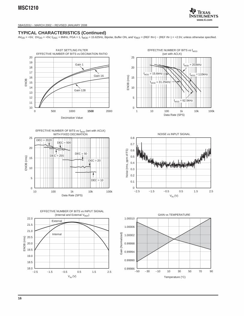
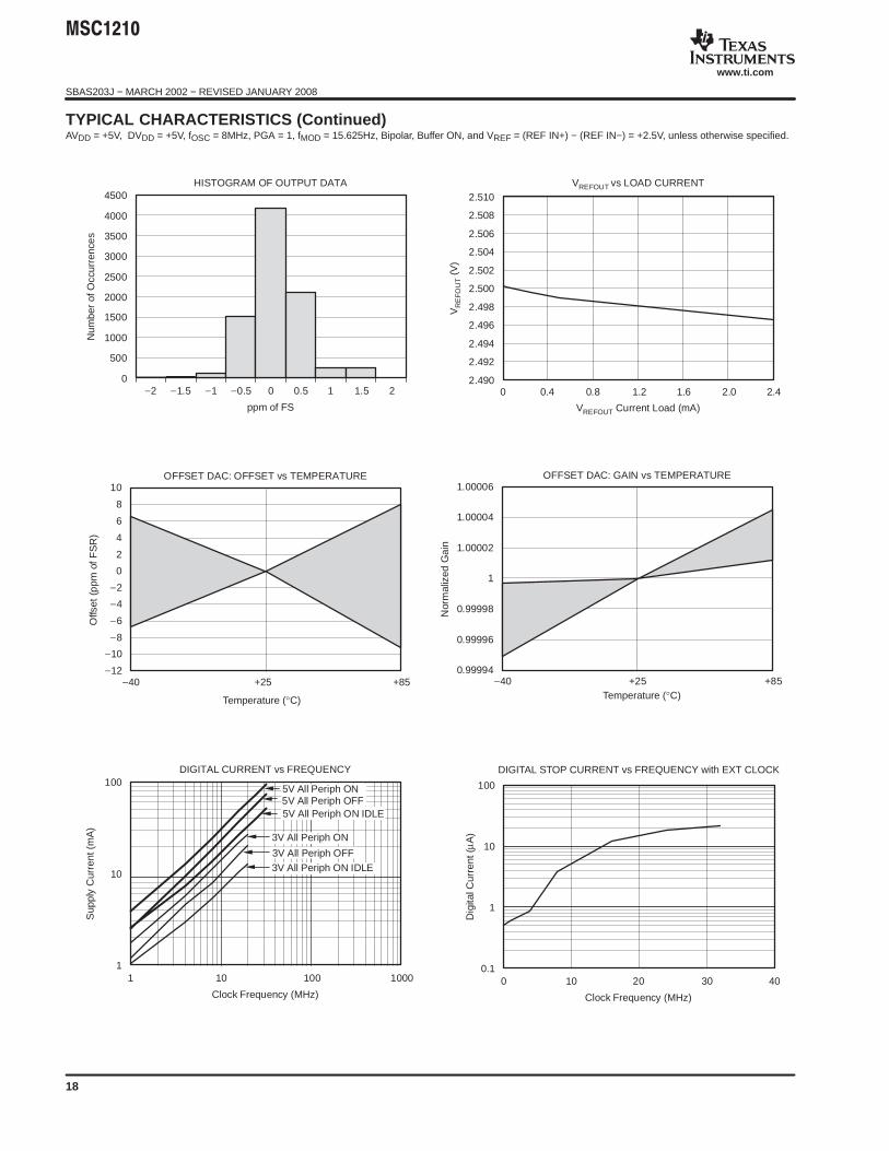
TYPICAL CHARACTERISTICSAVDD = +5V, DVDD = +5V, fOSC = 8MHz, PGA = 1, fMOD = 15.625Hz, Bipolar, Buffer ON, and VREF = (REF IN+) − (REF IN−) = +2.5V, unless otherwise specified.
EFFECTIVE NUMBER OF BITS vs DATA RATE2322212019181716151413121110
EN
OB
(rm
s)
Data Rate (SPS)1 10 100 1000
Sinc3 Filter, Buffer OFF
PGA1PGA8
PGA32PGA64
PGA128
22
21
20
19
18
17
16
15
14
13
12
EFFECTIVE NUMBER OF BITSvs DECIMATION RATIO
Decimation Ratio =fMOD
fDATA
0 500 1000 1500 2000
PGA4
EN
OB
(rm
s)
PGA1 PGA2
PGA16
PGA8
PGA32 PGA64 PGA128
Sinc3 Filter, Buffer OFF
22
21
20
19
18
17
16
15
14
13
12
EFFECTIVE NUMBER OF BITSvs DECIMATION RATIO
0 500 1000 1500 2000
EN
OB
(rm
s)
PGA4 PGA8
PGA1
PGA2
PGA16
PGA32 PGA64 PGA128
Decimation Ratio =fMOD
fDATA
Sinc3 Filter, Buffer ON
22
21
20
19
18
17
16
15
14
13
12
EFFECTIVE NUMBER OF BITSvs DECIMATION RATIO
0 500 1000 1500 2000
EN
OB
(rm
s)
PGA4 PGA8PGA1 PGA2
PGA16PGA32
PGA64 PGA128
Decimation Ratio =fMOD
fDATA
AVDD = 3V, Sinc3 Filter,VREF = 1.25V, Buffer OFF
22
21
20
19
18
17
16
15
14
13
12
EFFECTIVE NUMBER OF BITSvs DECIMATION RATIO
0 500 1000 1500 2000
EN
OB
(rm
s)
PGA4 PGA8
PGA1
PGA2
PGA16 PGA32 PGA64 PGA128
Decimation Ratio =fMOD
fDATA
AVDD = 3V, Sinc3 Filter,VREF = 1.25V, Buffer ON
22
21
20
19
18
17
16
15
14
13
12
EFFECTIVE NUMBER OF BITSvs DECIMATION RATIO
0 500 1000 1500 2000
EN
OB
(rm
s)
PGA4 PGA8
PGA1
PGA2
PGA32 PGA128PGA16 PGA64
Decimation Ratio =fMOD
fDATA
Sinc2 Filter
"#$%$&
SBAS203J − MARCH 2002 − REVISED JANUARY 2008
www.ti.com
16
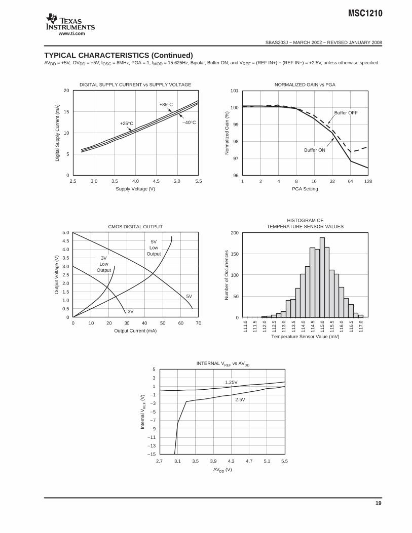
TYPICAL CHARACTERISTICS (Continued)AVDD = +5V, DVDD = +5V, fOSC = 8MHz, PGA = 1, fMOD = 15.625Hz, Bipolar, Buffer ON, and VREF = (REF IN+) − (REF IN−) = +2.5V, unless otherwise specified.
20
19
18
17
16
15
14
13
12
11
10
FAST SETTLING FILTEREFFECTIVE NUMBER OF BITS vs DECIMATION RATIO
0 500 1000
Gain 1
Gain 16
Gain 128
1500 2000
EN
OB
1500
Decimation Value
EFFECTIVE NUMBER OF BITS vs fMOD(set with ACLK)
25
20
15
10
5
0
EN
OB
(rm
s)
Data Rate (SPS)1 10 100 1k 10k 100k
fMOD = 15.6kHz
fMOD = 62.5kHz
fMOD = 203kHz
fMOD = 110kHz
fMOD = 31.25kHz
EFFECTIVE NUMBER OF BITS vs fMOD (set with ACLK)WITH FIXED DECIMATION
25
20
15
10
5
0
EN
OB
(rm
s)
Data Rate (SPS)10 100 1k 10k 100k
DEC = 2020
DEC = 255
DEC = 500
DEC = 50
DEC = 20
DEC = 10
0.8
0.7
0.6
0.5
0.4
0.3
0.2
0.1
0
NOISE vs INPUT SIGNAL
VIN (V)
−2.5 −1.5 0.5−0.5 1.5 2.5
No
ise
(rm
s,pp
mo
fFS
)
22.0
21.5
21.0
20.5
20.0
19.5
19.0
18.5
18.0
EFFECTIVE NUMBER OF BITS vs INPUT SIGNAL(Internal and External VREF)
VIN (V)
−2.5 −1.5 0.5−0.5 1.5 2.5
EN
OB
(rm
s)
External
Internal
1.00010
1.00006
1.00002
0.99998
0.99994
0.99990
0.99986
GAIN vs TEMPERATURE
−50 −30 10−10 30 50 70 90
Gai
n(N
orm
aliz
ed)
Temperature ( C)°

"#$%$&
SBAS203J − MARCH 2002 − REVISED JANUARY 2008
www.ti.com
17
TYPICAL CHARACTERISTICS (Continued)AVDD = +5V, DVDD = +5V, fOSC = 8MHz, PGA = 1, fMOD = 15.625Hz, Bipolar, Buffer ON, and VREF = (REF IN+) − (REF IN−) = +2.5V, unless otherwise specified.
10
8
6
4
2
0
−2
−4
−6
−8
−10
INTEGRAL NONLINEARITY vs INPUT SIGNAL
VIN (V)
−2.5 −2 −1 −0.5−1.5 0 0.5 1 1.5 2 2.5
INL
(ppm
ofF
S)
−40C
+25C
+85C
30
20
10
0
−10
−20
−30
INTEGRAL NONLINEARITY vs INPUT SIGNAL
VIN (V)
VIN = −VREF 0 VIN = +VREF
VREF = AVDD, Buffer OFF
INL
(ppm
ofF
S)
35
30
25
20
15
10
5
0
ADC INTEGRAL NONLINEARITY vs VREF
VREF (V)
0 0.5 1.0 1.5 2.0 2.5 3.0 3.5 4.0 4.5 5.0 5.5
AD
CIN
L(p
pm
ofF
S)
Buffer OFF
AVDD = 3V
AVDD = 5V
INL ERROR vs PGA
PGA Setting
INL
(ppm
ofF
S)
1 42 168 1286432
100
90
80
70
60
50
40
30
20
10
0
1.6
1.5
1.4
1.3
1.2
1.1
1.0
0.9
0.8
0.7
0.6
0.5
MAXIMUM ANALOG SUPPLY CURRENT
Analog Supply Voltage (V)
2.5 3.0 3.5 4.0 4.5 5.0 5.5
An
alo
gS
upp
lyC
urre
nt(m
A)
PGA = 128ADC ONBrownout Detect ON
−40C
+25C
+85C900
800
700
600
500
400
300
200
100
0
ADC CURRENT vs PGA
PGA Setting
0 1 82 4 3216 12864
I AD
C(
A)
AVDD = 5V, Buffer = ON
AVDD = 3V, Buffer = ON
Buffer = OFF
Buffer = OFF
µ
"#$%$&
SBAS203J − MARCH 2002 − REVISED JANUARY 2008
www.ti.com
18
TYPICAL CHARACTERISTICS (Continued)AVDD = +5V, DVDD = +5V, fOSC = 8MHz, PGA = 1, fMOD = 15.625Hz, Bipolar, Buffer ON, and VREF = (REF IN+) − (REF IN−) = +2.5V, unless otherwise specified.
4500
4000
3500
3000
2500
2000
1500
1000
500
0
HISTOGRAM OF OUTPUT DATA
ppm of FS
−2
Num
ber
ofO
ccur
renc
es
−1.5 −1 −0.5 0 0.5 1 1.5 2
2.510
2.508
2.506
2.504
2.502
2.500
2.498
2.496
2.494
2.492
2.490
VREFOUT vs LOAD CURRENT
VREFOUT Current Load (mA)
0 0.4 0.8 1.2 1.6 2.0 2.4
VR
EFO
UT
(V)
10
8
6
4
2
0
−2
−4
−6
−8
−10
−12
OFFSET DAC: OFFSET vs TEMPERATURE
Offs
et(p
pmof
FS
R)
−40 +25 +85
Temperature (°C)
1.00006
1.00004
1.00002
1
0.99998
0.99996
0.99994
OFFSET DAC: GAIN vs TEMPERATURE
Nor
mal
ized
Ga
in
−40 +25 +85Temperature (°C)
DIGITAL CURRENT vs FREQUENCY
Clock Frequency (MHz)
Sup
ply
Cur
rent
(mA
)
1 10 100 1000
100
10
1
5V All Periph ON5V All Periph OFF5V All Periph ON IDLE
3V All Periph ON
3V All Periph OFF3V All Periph ON IDLE
Clock Frequency (MHz)
Dig
italC
urre
nt(µ
A)
0 10 20 4030
100
10
1
0.1
DIGITAL STOP CURRENT vs FREQUENCY with EXT CLOCK
"#$%$&
SBAS203J − MARCH 2002 − REVISED JANUARY 2008
www.ti.com
19
TYPICAL CHARACTERISTICS (Continued)AVDD = +5V, DVDD = +5V, fOSC = 8MHz, PGA = 1, fMOD = 15.625Hz, Bipolar, Buffer ON, and VREF = (REF IN+) − (REF IN−) = +2.5V, unless otherwise specified.
DIGITAL SUPPLY CURRENT vs SUPPLY VOLTAGE
Supply Voltage (V)
Dig
italS
uppl
yC
urre
nt(m
A)
2.5 3.0 3.5 4.0 4.5 5.0 5.5
20
15
10
5
0
−40 C
+85 C
+25 C °°
°
NORMALIZED GAIN vs PGA
PGA Setting
Nor
mal
ized
Gai
n(%
)
1 42 168 1286432
101
100
99
98
97
96
Buffer ON
Buffer OFF
CMOS DIGITAL OUTPUT
Output Current (mA)
Ou
tput
Vol
tage
(V)
0 2010 4030 706050
5.0
4.5
4.0
3.5
3.0
2.5
2.0
1.5
1.0
0.5
0
3VLow
Output
5VLow
Output
5V
3V
200
150
100
50
0
HISTOGRAM OFTEMPERATURE SENSOR VALUES
Temperature Sensor Value (mV)
111
.0
111
.5
112
.0
112
.5
113
.0
113
.5
114
.0
114
.5
115
.0
115
.5
116
.0
116
.5
117
.0
Num
ber
ofO
ccu
rren
ces
5
3
1
−1
−3
−5
−7
−9
−11
−13
−15
Inte
rna
lVR
EF
(V)
2.7 3.1 3.5 3.9 4.3 4.7 5.1 5.5
AVDD (V)
1.25V
2.5V
INTERNAL VREF vs AVDD

"#$%$&
SBAS203J − MARCH 2002 − REVISED JANUARY 2008
www.ti.com
20
DESCRIPTIONThe MSC1210Yx is a completely integrated family ofmixed-signal devices incorporating a high-resolutiondelta-sigma ADC, 8-channel multiplexer, burnout currentsources, selectable buffered input, offset DAC(digital-to-analog converter), PGA (programmable gainamplifier), temperature sensor, voltage reference, 8-bitmicrocontroller, Flash Program Memory, Flash DataMemory, and Data SRAM, as shown in Figure 8.
On-chip peripherals include an additional 32-bitaccumulator, an SPI-compatible serial port, dual USARTs,multiple digital input/output ports, watchdog timer,low-voltage detect, on-chip power-on reset, 16-bit PWM,and system timers, brownout reset, and threetimer/counters.
The device accepts low-level differential or single-endedsignals directly from a transducer. The ADC provides 24bits of resolution and 24 bits of no-missing-codeperformance using a Sinc3 filter with a programmablesample rate. The ADC also has a selectable filter thatallows for high-resolution single-cycle conversion.
The microcontroller core is 8051 instruction setcompatible. The microcontroller core is an optimized 8051core that executes up to three times faster than thestandard 8051 core, given the same clock source. Thatmakes it possible to run the device at a lower external clockfrequency and achieve the same performance at lowerpower than the standard 8051 core.
The MSC1210Yx allows the user to uniquely configure theFlash and SRAM memory maps to meet the needs of theirapplication. The Flash is programmable down to 2.7Vusing both serial and parallel programming methods. TheFlash endurance is 1 million Erase/Write cycles. Inaddition, 1280 bytes of RAM are incorporated on-chip.
The part has separate analog and digital supplies, whichcan be independently powered from 2.7V to +5.25V. At+3V operation, the power dissipation for the part istypically less than 4mW. The MSC1210Yx is packaged ina TQFP-64 package.
The MSC1210Yx is designed for high-resolutionmeasurement applications in smart transmitters, industrialprocess control, weigh scales, chromatography, andportable instrumentation.
ACC
MUX
AGND
+AVDD
AVDD
BUFFER PGA
VREF
Modulator
Up to 32KFLASH
1.2KSRAM
SPI
DigitalFilter
8051
SFR
LVD
BOR
PORT1
PORT2
WDT
Timers/Counters
ClockGenerator
PORT0
PORT3
8
8
8
EA
8
T2SPI/EXTUSART2
ADDR
ADDRDATA
AlternateFunctions
USART1EXTT0T1RW
8−BitPGA OffsetAIN0
AIN1
AIN2
AIN3
AIN4
AIN5
AIN6
AIN7
AINCOM
AGND REF OUT REF IN+ REF IN− DVDD DGND
XIN XOUT
ALE
PSEN
RSTPOR
TemperatureSensor
REF
NOTE (1) REF IN− must be tied to AGND when using internal VREF.
(1)
Figure 8. Block Diagram

"#$%$&
SBAS203J − MARCH 2002 − REVISED JANUARY 2008
www.ti.com
21
ENHANCED 8051 COREAll instructions in the MSC1210 family perform exactly thesame functions as they would in a standard 8051. Theeffect on bits, flags, and registers is the same. However,the timing is different. The MSC1210 family utilizes anefficient 8051 core which results in an improved instructionexecution speed of between 1.5 and 3 times faster than theoriginal core for the same external clock speed (4 clockcycles per instruction versus 12 clock cycles perinstruction, as shown in Figure 9). The internal systemclock is equal to the external oscillator frequency. Thistranslates into an effective throughput improvement ofmore than 2.5 times, using the same code and sameexternal clock speed.
Therefore, a device frequency of 33MHz for theMSC1210Yx actually performs at an equivalent executionspeed of 82.5MHz compared to the standard 8051 core.This allows the user to run the device at slower externalclock speeds which reduces system noise and powerconsumption, but provides greater throughput. Thisperformance difference can be seen in Figure 10. Thetiming of software loops will be faster with the MSC1210.However, the timer/counter operation of the MSC1210may be maintained at 12 clocks per increment or optionallyrun at 4 clocks per increment.
The MSC1210 also provides dual data pointers (DPTRs)to speed block Data Memory moves.
Additionally, it can stretch the number of memory cycles toaccess external Data Memory from between two and nineinstruction cycles in order to accommodate differentspeeds of memory or devices, as shown in Table 1. TheMSC1210 provides an external memory interface with a16-bit address bus (P0 and P2). The 16-bit address busmakes it necessary to multiplex the low address bytethrough the P0 port. To enhance P0 and P2 for high-speedmemory access, hardware configuration control isprovided to configure the ports for externalmemory/peripheral interface or general-purpose I/O.
ALE
PSEN
AD0−AD7
PORT 2
ALE
PSEN
AD0−AD7
PORT 2
CLK
Sta
ndar
d80
51T
imin
gM
SC
121
Tim
ing
Single−Byte, Single−CycleInstruction
Instruction
12 Cycles
4 Cycles
0
Single−Byte, Single−Cycle
Figure 10. Comparison of MSC1210 Timing toStandard 8051 Timing
Table 1. Memory Cycle Stretching. Stretching ofMOVX timing as defined by MD2, MD1, and MD0
bits in CKCON register (address 8Eh).
CKCON(8Eh)
MD2:MD0
INSTRUCTIONCYCLES
(for MOVX)
RD or WRSTROBE WIDTH
(SYS CLKs)
RD or WRSTROBE WIDTH(s) AT 12MHz
000 2 2 0.167
001 3 (default) 4 0.333
010 4 8 0.667
011 5 12 1.000
100 6 16 1.333
101 7 20 1.667
110 8 24 2.000
111 9 28 2.333
CLK
instr_cycle
cpu_cycle C1 C2 C3 C4 C1 C2 C3 C4 C1
n + 1 n + 2
Figure 9. Instruction Timing Cycle
"#$%$&
SBAS203J − MARCH 2002 − REVISED JANUARY 2008
www.ti.com
22
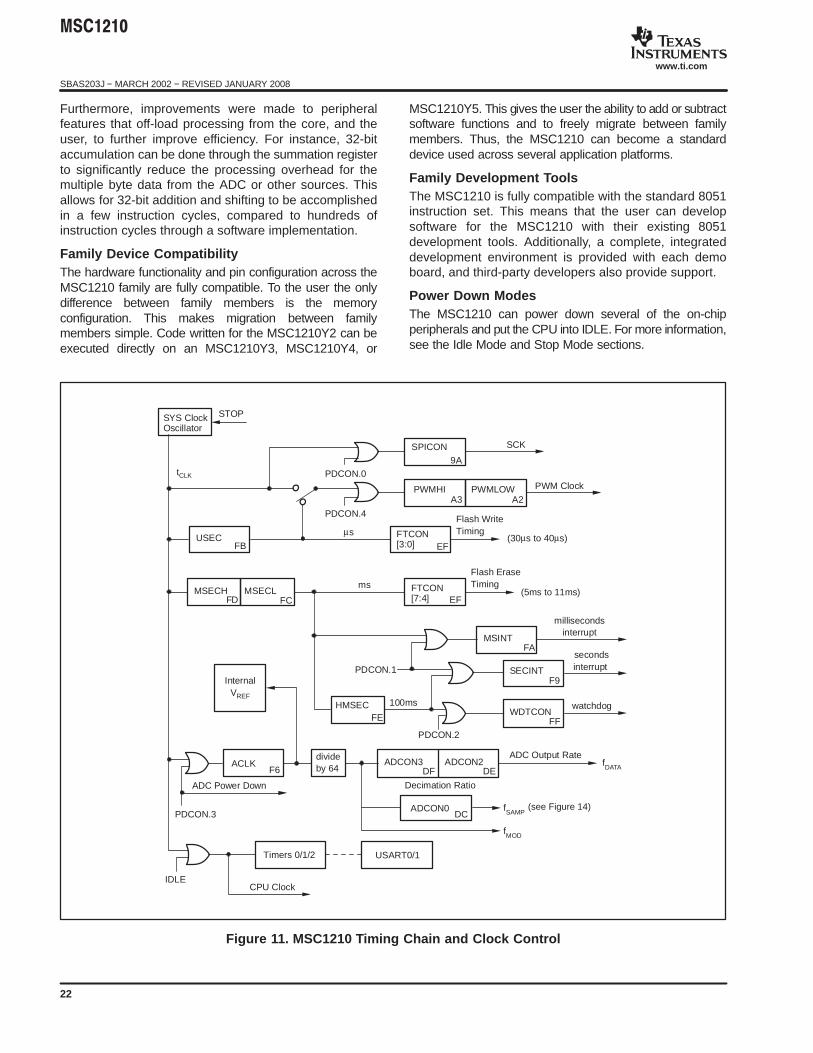
Furthermore, improvements were made to peripheralfeatures that off-load processing from the core, and theuser, to further improve efficiency. For instance, 32-bitaccumulation can be done through the summation registerto significantly reduce the processing overhead for themultiple byte data from the ADC or other sources. Thisallows for 32-bit addition and shifting to be accomplishedin a few instruction cycles, compared to hundreds ofinstruction cycles through a software implementation.
Family Device CompatibilityThe hardware functionality and pin configuration across theMSC1210 family are fully compatible. To the user the onlydifference between family members is the memoryconfiguration. This makes migration between familymembers simple. Code written for the MSC1210Y2 can beexecuted directly on an MSC1210Y3, MSC1210Y4, or
MSC1210Y5. This gives the user the ability to add or subtractsoftware functions and to freely migrate between familymembers. Thus, the MSC1210 can become a standarddevice used across several application platforms.
Family Development ToolsThe MSC1210 is fully compatible with the standard 8051instruction set. This means that the user can developsoftware for the MSC1210 with their existing 8051development tools. Additionally, a complete, integrateddevelopment environment is provided with each demoboard, and third-party developers also provide support.
Power Down ModesThe MSC1210 can power down several of the on-chipperipherals and put the CPU into IDLE. For more information,see the Idle Mode and Stop Mode sections.
USECFB
MSECH
HMSECFE
MSINTFA
ACLKF6
divideby 64
InternalVREF
MSECLFD FC
ms
µs
100ms
Flash WriteTiming
Flash EraseTiming
WDTCON
SECINTF9
FF
FTCON[3:0]
FTCON[7:4]
EF
EF
secondsinterrupt
watchdog
millisecondsinterrupt
ADC Output RateADCON3 ADCON2
DF DE
Decimation Ratio
SYS ClockOscillator
PWMHI PWMLOWA3 A2
PWM Clock
SPICON9A
SCK
tCLK
(30µs to 40µs)
(5ms to 11ms)
STOP
PDCON.0
PDCON.4
PDCON.1
PDCON.2
PDCON.3
IDLECPU Clock
Timers 0/1/2
ADC Power Down
USART0/1
ADCON0DC
fSAMP
fDATA
fMOD
(see Figure 14)
Figure 11. MSC1210 Timing Chain and Clock Control
"#$%$&
SBAS203J − MARCH 2002 − REVISED JANUARY 2008
www.ti.com
23
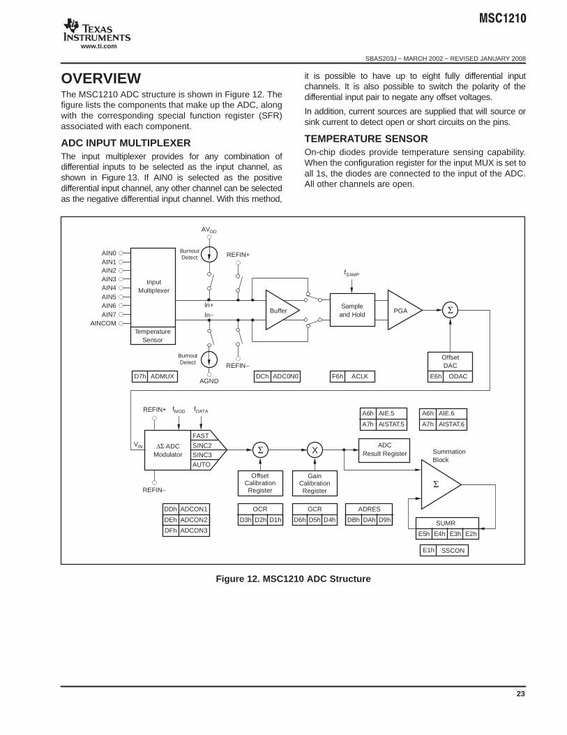
OVERVIEWThe MSC1210 ADC structure is shown in Figure 12. Thefigure lists the components that make up the ADC, alongwith the corresponding special function register (SFR)associated with each component.
ADC INPUT MULTIPLEXERThe input multiplexer provides for any combination ofdifferential inputs to be selected as the input channel, asshown in Figure 13. If AIN0 is selected as the positivedifferential input channel, any other channel can be selectedas the negative differential input channel. With this method,
it is possible to have up to eight fully differential inputchannels. It is also possible to switch the polarity of thedifferential input pair to negate any offset voltages.
In addition, current sources are supplied that will source orsink current to detect open or short circuits on the pins.
TEMPERATURE SENSOROn-chip diodes provide temperature sensing capability.When the configuration register for the input MUX is set toall 1s, the diodes are connected to the input of the ADC.All other channels are open.
Σ
Σ X
InputMultiplexer
TemperatureSensor
Buffer PGASample
and Hold
ADMUXD7h
REFIN+
REFIN−
REFIN+ fMOD
REFIN−
AIN5AIN6AIN7
AINCOM
ADCON1DDh
ADCON2DEh
ADCON3DFh
OCR GCR ADRES
SUMRD3h D2h D1h D6h D5h D4h DBh DAh D9h
E5h E4h E3h E2h
OffsetCalibrationRegister
ADC0N0DCh ACLKF6h
SSCONE1h
ODACE6h
OffsetDAC
∆Σ ADCModulator
FAST
SINC2SINC3
AUTO
ADCResult Register
Σ
SummationBlock
VIN
AIN2AIN3AIN4
AIN0AIN1
fSAMP
fDATA
GainCalibrationRegister
BurnoutDetect
AVDD
In+
AGND
In−
BurnoutDetect
AISTAT.5A7h
AIE.5A6h
AISTAT.6A7h
AIE.6A6h
Figure 12. MSC1210 ADC Structure

"#$%$&
SBAS203J − MARCH 2002 − REVISED JANUARY 2008
www.ti.com
24
AIN3
AIN4
AIN5
AIN6
AIN0
AIN1
AIN2
AIN7
AINCOM
Burnout DetectCurrent Source
Burnout DetectCurrent Sink
AGND
Temperature Sensor
I80 • I
AVDD
In+
In−
Figure 13. Input Multiplexer Configuration
BURNOUT DETECT
When the Burnout Detect (BOD) bit is set in the ADCcontrol configuration register (ADCON0 DCh), two currentsources are enabled. The current source on the positiveinput channel sources approximately 2µA of current. Thecurrent source on the negative input channel sinksapproximately 2µA. This allows for the detection of anopen circuit (full-scale reading) or short circuit (smalldifferential reading) on the selected input differential pair.Buffer should be on for sensor burnout detection.
ADC INPUT BUFFER
The analog input impedance is always high, regardless ofPGA setting (when the buffer is enabled). With the bufferenabled, the input voltage range is reduced and the analogpower-supply current is higher. If the limitation of inputvoltage range is acceptable, then the buffer is alwayspreferred.
The input impedance of the MSC1210 without the buffer is7MΩ/PGA. The buffer is controlled by the state of the BUFbit in the ADC control register (ADCON0 DCh).
ADC ANALOG INPUT
When the buffer is not selected, the input impedance of theanalog input changes with ACLK clock frequency (ACLKF6h) and gain (PGA). The relationship is:
Impedance () 1fSAMP CS
AIN Impedance() 106
ACLK Frequency 7M
PGA
where ACLK frequency fCLK
(ACLK1)
and modclk fMOD fACLK
64.
NOTE: The input impedance for PGA = 128 is the same as that for
PGA = 64 ( that is, 7M
64).
Figure 14 shows the basic input structure of the MSC1210.
BIPOLAR MODE UNIPOLAR MODEPGA FULL-SCALE RANGE FULL-SCALE RANGE f SAMP
1 ±VREF +VREF fMOD2 ±VREF/2 +VREF/2 fMOD4 ±VREF/4 +VREF/4 fMOD8 ±VREF/8 +VREF/8 fMOD 216 ±VREF/16 +VREF/16 fMOD 432 ±VREF/32 +VREF/32 fMOD 864 ±VREF/64 +VREF/64 fMOD 16128 ±VREF/128 +VREF/128 fMOD 16
NOTE: fMOD = ACLK frequency/64
RSWITCH(3k typical)
SamplingFrequency = fSAMP
HighImpedance
> 1GΩCS
AGND
AIN
(9pF typical)
PGA CS1 9pF2 18pF
4 to 128 36pF
Figure 14. Analog Input Structure

"#$%$&
SBAS203J − MARCH 2002 − REVISED JANUARY 2008
www.ti.com
25
ADC PGAThe PGA can be set to gains of 1, 2, 4, 8, 16, 32, 64, or 128.Using the PGA can actually improve the effectiveresolution of the ADC. For instance, with a PGA of 1 on a±2.5V full-scale range, the ADC can resolve to 1.5µV. Witha PGA of 128 on a ±19mV full-scale range, the ADC canresolve to 75nV, as shown in Table 2.
Table 2. ENOB versus PGA (Bipolar Mode)
PGASETTING
FULL-SCALERANGE (V)
ENOB(1)
AT 10HZRMS MEASUREMENT
RESOLUTION (nV)
1 ±2.5V 21.7 1468
2 ±1.25 21.5 843
4 ±0.625 21.4 452
8 ±0.313 21.2 259
16 ±0.156 20.8 171
32 ±0.0781 20.4 113
64 ±0.039 20 74.5
128 ±0.019 19 74.5
(1) ENOB = Log2(FSR/RMS Noise) = Log2(224) − Log2(σCODES)= 24 − Log2(σCODES)
ADC OFFSET DAC
The analog input to the PGA can be offset (in bipolar mode)by up to half the full-scale input range of the PGA by usingthe ODAC register (SFR E6h). The ODAC (Offset DAC)register is an 8-bit value; the MSB is the sign and the sevenLSBs provide the magnitude of the offset. Since the ODACintroduces an analog (instead of digital) offset to the PGA,using the ODAC does not reduce the range of the ADC.
ADC MODULATORThe modulator is a single-loop 2nd-order system. Themodulator runs at a clock speed (fMOD) that is derived fromthe CLK using the value in the Analog Clock (ACLK)register (SFR F6h). The data rate is:
Data Rate fMOD
Decimation Ratio
where fMOD fCLK
(ACLK1) 64
fACLK
64
and Decimation Ratio is set in [ADCON3:ADCON2].
ADC CALIBRATION
The offset and gain errors in the MSC1210, or thecomplete system, can be reduced with calibration.Calibration is controlled through the ADCON1 register(SFR DDh), bits CAL2:CAL0. Each calibration processtakes seven tDATA (data conversion time) periods tocomplete. Therefore, it takes 14 tDATA periods to completeboth an offset and gain calibration.
For system calibration, the appropriate signal must beapplied to the inputs. The system offset command requiresa zero differential input signal. It then computes an offsetvalue that will nullify offsets in the system. The system gaincommand requires a positive full-scale differential inputsignal. It then computes a value to nullify gain errors in thesystem. Each of these calibrations will take seven tDATAperiods to complete.
Calibration should be performed after power on. It shouldalso be done after a change in temperature, decimationratio, buffer, Power Supply, voltage reference, or PGA.The Offset DAC wil affect offset calibration; therefore, thevalue of the Offset DAC should be zero until prior toperforming a calibration.
At the completion of calibration, the ADC Interrupt bit goesHIGH which indicates the calibration is finished and validdata is available.
ADC DIGITAL FILTER
The Digital Filter can use either the Fast Settling, Sinc2, orSinc3 filter, as shown in Figure 15. In addition, the Automode changes the Sinc filter after the input channel orPGA is changed. When switching to a new channel or newPGA value, it will use the Fast Settling filter for the next twoconversions (the first of which should be discarded). It willthen use the Sinc2 followed by the Sinc3 filter to improvenoise performance.
Discard Fast Sinc2 Sinc3
1 2 3 4
FILTERSETTLING TIME
(Conversion Cycles) (1)
Sinc3 Sinc2 Fast
321
NOTE: (1) MUX change may add one cycle.
CONVERSION CYCLEAUTO MODE FILTER SELECTION
FILTER SETTLING TIME
Adjustable Digital Filter
Data OutModulator
Fast Settling
Sinc2
Sinc3
Figure 15. Filter Step Responses
"#$%$&
SBAS203J − MARCH 2002 − REVISED JANUARY 2008
www.ti.com
26
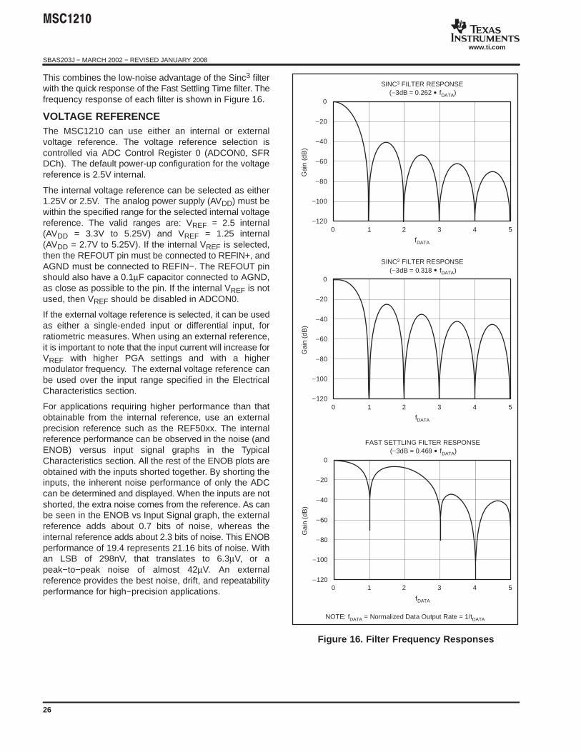
This combines the low-noise advantage of the Sinc3 filterwith the quick response of the Fast Settling Time filter. Thefrequency response of each filter is shown in Figure 16.
VOLTAGE REFERENCEThe MSC1210 can use either an internal or externalvoltage reference. The voltage reference selection iscontrolled via ADC Control Register 0 (ADCON0, SFRDCh). The default power-up configuration for the voltagereference is 2.5V internal.
The internal voltage reference can be selected as either1.25V or 2.5V. The analog power supply (AVDD) must bewithin the specified range for the selected internal voltagereference. The valid ranges are: VREF = 2.5 internal(AVDD = 3.3V to 5.25V) and VREF = 1.25 internal(AVDD = 2.7V to 5.25V). If the internal VREF is selected,then the REFOUT pin must be connected to REFIN+, andAGND must be connected to REFIN−. The REFOUT pinshould also have a 0.1µF capacitor connected to AGND,as close as possible to the pin. If the internal VREF is notused, then VREF should be disabled in ADCON0.
If the external voltage reference is selected, it can be usedas either a single-ended input or differential input, forratiometric measures. When using an external reference,it is important to note that the input current will increase forVREF with higher PGA settings and with a highermodulator frequency. The external voltage reference canbe used over the input range specified in the ElectricalCharacteristics section.
For applications requiring higher performance than thatobtainable from the internal reference, use an externalprecision reference such as the REF50xx. The internalreference performance can be observed in the noise (andENOB) versus input signal graphs in the TypicalCharacteristics section. All the rest of the ENOB plots areobtained with the inputs shorted together. By shorting theinputs, the inherent noise performance of only the ADCcan be determined and displayed. When the inputs are notshorted, the extra noise comes from the reference. As canbe seen in the ENOB vs Input Signal graph, the externalreference adds about 0.7 bits of noise, whereas theinternal reference adds about 2.3 bits of noise. This ENOBperformance of 19.4 represents 21.16 bits of noise. Withan LSB of 298nV, that translates to 6.3µV, or apeak−to−peak noise of almost 42µV. An externalreference provides the best noise, drift, and repeatabilityperformance for high−precision applications.
SINC3 FILTER RESPONSE(−3dB = 0.262 • fDATA)
fDATA
0
−20
−40
−60
−80
−100
−1200 1 2 3 4 5
0 1 2 3 4 5
0 1 2 3 4 5
Gai
n(d
B)
SINC2 FILTER RESPONSE(−3dB = 0.318 • fDATA)
fDATA
0
−20
−40
−60
−80
−100
−120
Gai
n(d
B)
FAST SETTLING FILTER RESPONSE(−3dB = 0.469 • fDATA)
fDATA
0
−20
−40
−60
−80
−100
−120
NOTE: fDATA = Normalized Data Output Rate = 1/tDATA
Gai
n(d
B)
Figure 16. Filter Frequency Responses

"#$%$&
SBAS203J − MARCH 2002 − REVISED JANUARY 2008
www.ti.com
27
RESET
The device can be reset from the following sources:
Power-on reset
External reset
Software reset
Watchdog timer reset
Brownout reset
An external reset is accomplished by taking the RST pinhigh for two tOSC periods, followed by taking the RST pinlow. A software reset is accomplished through the SystemReset register (SRTST, 0F7h). A watchdog timer reset isenabled and controlled through Hardware ConfigurationRegister 0 (HCR0) and the Watchdog Timer register(WDTCON, 0FFh). A brownout reset is enabled throughHardware Configuration Register 1 (HCR1). Externalreset, software reset, and watchdog timer reset completeafter 217 clock cycles. A brownout reset completes after 215
clock cycles.
All sources of reset cause the digital pins to be pulled highfrom the initiation of the reset. For an external reset, takingthe RST pin high stops device operation, crystaloscillation, and causes all digital pins to be pulled high fromthat point. Taking the RST pin low initiates the resetprocedure.
A recommended external reset circuit is shown inFigure 17. The serial 10kΩ resistor is recommended forany external reset circuit configuration.
10kΩ13 RST
MSC1210
0.1µF
1MΩ
DVDD
Figure 17. Typical Reset Circuit
POWER-ON RESET
The on-chip power-on reset (POR) circuitry releases thedevice from reset at approximately DVDD = 2.0V. The PORaccommodates power-supply ramp rates as slow as1V/10ms. To ensure proper operation, the power supplyshould ramp monotonically. Note that as the device isreleased from reset and program execution begins, thedevice current consumption may increase, which mayresult in a power-supply voltage drop. If the power supplyramps at a slower rate, is not monotonic, or a brownoutcondition occurs (where the supply does not drop belowthe 2.0V threshold), then improper device operation mayoccur. The on-chip brownout reset may provide benefit inthese conditions.
BROWNOUT RESET
The brownout reset (BOR) is enabled through HardwareConfiguration Register 1 (HCR1). If the conditions forproper POR are not met or the device encounters abrownout condition that does not generate a POR, theBOR can be used to ensure proper device operation. TheBOR will hold the state of the device when the powersupply drops below the threshold level programmed inHCR1, and then generate a reset when the supply risesabove the threshold level. Note that as the device isreleased from reset, and program execution begins, thedevice current consumption may increase, which mayresult in a power-supply voltage drop, which may initiateanother brownout condition.
The BOR level should be chosen to match closely with theapplication. For example, with a high external clockfrequency, the BOR level should match the minimumoperating voltage range for the device, or improperoperation may still occur.
Note that AVDD must rise above 2.0V for the AnalogBrownout Reset function to be disabled; otherwise, it willbe enabled and hold the device in reset.
The BOR voltage is not calibrated until the end of the resetcycle; therefore, the actual BOR voltage will beapproxiamtely 25% higher than the selected voltage. Thiscan create a condition where the reset never ends (forexample, when selecting a 4.5V BOR voltage for a 5Vpower supply).
"#$%$&
SBAS203J − MARCH 2002 − REVISED JANUARY 2008
www.ti.com
28
IDLE MODE
Idle mode is entered by setting the IDLE bit in the PowerControl register (PCON, 087h). In Idle mode, the CPU,Timer0, Timer1, and USARTs are stopped, but all otherperipherals and digital pins remain active. The device canbe returned to active mode via an active internal or externalinterrupt. This mode is typically used for reducing powerconsumption between ADC samples.
By configuring the device prior to entering Idle mode,further power reductions can be achieved (while in Idlemode). These reductions include powering downperipherals not in use in the PDCON register (0F1h).
STOP MODE
Stop mode is entered by setting the STOP bit in the PowerControl register (PCON, 087h). In Stop mode, all internalclocks are halted. This mode has the lowest powerconsumption. The device can be returned to active modeonly via an external or power-on reset.
By configuring the device prior to entering Stop mode,further power reductions can be achieved (while in Stopmode). These power reductions include halting theexternal clock into the device, configuring all digital I/Opins as open drain with low output drive, disabling the ADCbuffer, disabling the internal VREF, and setting PDCON to0FFh to power down all peripherals.
In Stop mode, if the brownout reset is enabled, there isapproximately 25µA of draw from the power supply. Toachieve zero current (≈ 100nA) in Stop mode, disable thebrownout reset via HCR1.
In Stop mode, all digital pins retain their values.
POWER CONSUMPTION CONSIDERATIONS
The following suggestions will reduce currentconsumption:
1. Use the lowest supply voltage that will work in theapplication for both AVDD and DVDD.
2. Use the lowest clock frequency that will work in theapplication.
3. Use Idle mode and the system clock divider wheneverpossible. Note that the system clock divider also affectsthe ADC clock.
4. Avoid using 8051-compatible I/O mode on the I/O ports.The internal pull-up resistors will draw current when theoutputs are low.
5. Use the delay line for Flash Memory control by setting theFRCM bit in the FMCON register (SFR EEh)
6. Power down peripherals when they are not needed.Refer to SFR PDCON, LVDCON, and ADCON0.
MEMORY MAP
The MSC1210 contains on-chip SFR, Flash Memory,Scratchpad SRAM Memory, Boot ROM, and SRAM. THeSFR registers are primarily used for control and status.The standard 8051 features and additional peripheralfeatures of the MSC1210 are controlled through the SFR.Reading from an undefined SFR and writing to undefinedSFR registers is not recommended, and will haveindeterminate effects.
Flash Memory is used for both Program Memory and DataMemory. The user has the ability to select the partition sizeof Program and Data Memories. The partition size is setthrough hardware configuration bits, which areprogrammed through either the parallel or serialprogramming methods. Both Program and Data FlashMemories are erasable and writable (programmable) inUser Application mode (UAM). However, programexecution can only occur from Program Memory.As an added precaution, a lock feature can be activatedthrough the hardware configuration bits, which disableserase and writes to 4kB of Program Flash Memory or theentire Program Flash Memory in UAM.
The MSC1210 includes 1kB of SRAM on-chip. SRAM startsat address 0 and is accessed through the MOVX instruction.This SRAM can also be located to start at 8400h and can beaccessed as both Program and Data Memory.
"#$%$&
SBAS203J − MARCH 2002 − REVISED JANUARY 2008
www.ti.com
29
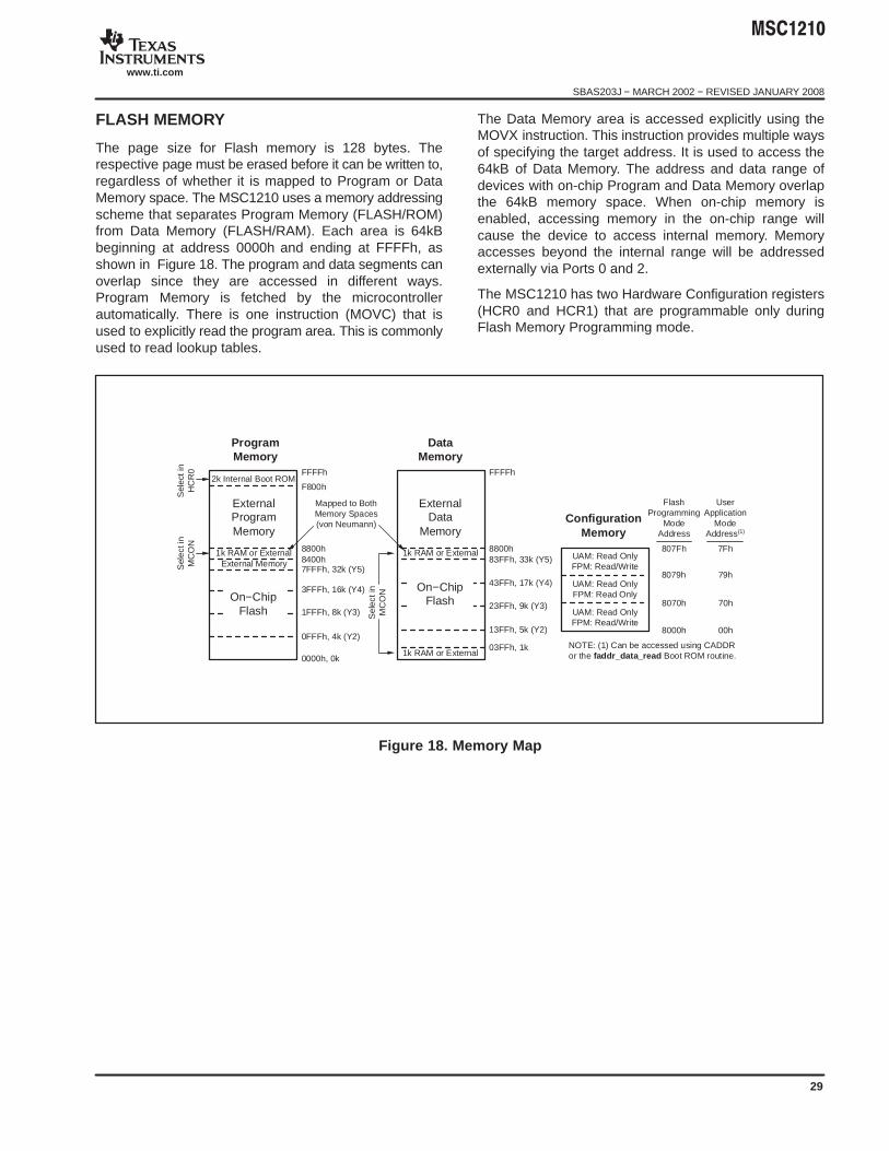
FLASH MEMORY
The page size for Flash memory is 128 bytes. Therespective page must be erased before it can be written to,regardless of whether it is mapped to Program or DataMemory space. The MSC1210 uses a memory addressingscheme that separates Program Memory (FLASH/ROM)from Data Memory (FLASH/RAM). Each area is 64kBbeginning at address 0000h and ending at FFFFh, asshown in Figure 18. The program and data segments canoverlap since they are accessed in different ways.Program Memory is fetched by the microcontrollerautomatically. There is one instruction (MOVC) that isused to explicitly read the program area. This is commonlyused to read lookup tables.
The Data Memory area is accessed explicitly using theMOVX instruction. This instruction provides multiple waysof specifying the target address. It is used to access the64kB of Data Memory. The address and data range ofdevices with on-chip Program and Data Memory overlapthe 64kB memory space. When on-chip memory isenabled, accessing memory in the on-chip range willcause the device to access internal memory. Memoryaccesses beyond the internal range will be addressedexternally via Ports 0 and 2.
The MSC1210 has two Hardware Configuration registers(HCR0 and HCR1) that are programmable only duringFlash Memory Programming mode.
1k RAM or External1k RAM or External
1k RAM or External
External MemorySel
ecti
nM
CO
NS
elec
tin
HC
R0
0000h, 0k
1FFFh, 8k (Y3)
0FFFh, 4k (Y2)
3FFFh, 16k (Y4)
8400h7FFFh, 32k (Y5)
2k Internal Boot ROMF800h
FFFFh
ExternalProgramMemory
Mapped to BothMemory Spaces(von Neumann)
8800h
Sel
ecti
nM
CO
N
03FFh, 1k
13FFh, 5k (Y2)
23FFh, 9k (Y3)
43FFh, 17k (Y4)
83FFh, 33k (Y5)
FFFFh
ExternalData
Memory
ProgramMemory
DataMemory
8800h
On−ChipFlash
On−ChipFlash
FlashProgramming
ModeAddress
UserApplication
ModeAddress(1)
NOTE: (1) Can be accessed using CADDRor the faddr_data_read Boot ROM routine.
UAM: Read OnlyFPM: Read Only
UAM: Read OnlyFPM: Read/Write
UAM: Read OnlyFPM: Read/Write
807Fh
8000h
8070h
7Fh
8079h 79h
00h
70h
ConfigurationMemory
Figure 18. Memory Map

"#$%$&
SBAS203J − MARCH 2002 − REVISED JANUARY 2008
www.ti.com
30
The MSC1210 allows the user to partition the FlashMemory between Program Memory and Data Memory. Forinstance, the MSC1210Y5 contains 32kB of FlashMemory on-chip. Through the HW configuration registers,the user can define the partition between ProgramMemory (PM) and Data Memory (DM), as shown in Table 3and Table 4. The MSC1210 family offers four memoryconfigurations, as shown.
Table 3. MSC1210 Flash Partitioning
HCR0 MSC1210Y2 MSC1210Y3 MSC1210Y4 MSC1210Y5
DFSEL PM DM PM DM PM DM PM DM
000 0kB 4kB 0kB 8kB 0kB 16kB 0kB 32kB
001 0kB 4kB 0kB 8kB 0kB 16kB 0kB 32kB
010 0kB 4kB 0kB 8kB 0kB 16kB 16kB 16kB
011 0kB 4kB 0kB 8kB 8kB 8kB 24kB 8kB
100 0kB 4kB 4kB 4kB 12kB 4kB 28kB 4kB
101 2kB 2kB 6kB 2kB 14kB 2kB 30kB 2kB
110 3kB 1kB 7kB 1kB 15kB 1kB 31kB 1kB
111(default)
4kB 0kB 8kB 0kB 16kB 0kB 32kB 0kB
NOTE: When a 0kB program memory configuration is selected, programexecution is external.
Table 4. MSC1210 Flash Memory Partitioning
HCR0 MSC1210Y2 MSC1210Y3 MSC1210Y4 MSC1210Y5
DFSEL PM DM PM DM PM DM PM DM
000 00000400-13FF
00000400-23FF
00000400-43FF
00000400-83FF
001 00000400-13FF
00000400-23FF
00000400-43FF
00000400-83FF
010 00000400-13FF
00000400-23FF
00000400-43FF
0000-3FFF
0400-43FF
011 00000400-13FF
00000400-23FF
0000-1FFF
0400-23FF
0000-5FFF
0400-23FF
100 00000400-13FF
0000-0FFF
0400-13FF
0000-2FFF
0400-13FF
0000-6FFF
0400-13FF
1010000-07FF
0400-0BFF
0000-17FF
0400-0BFF
0000-37FF
0400-0BFF
0000-77FF
0400-0BFF
1100000-0BFF
0400-07FF
0000-1BFF
0400-07FF
0000-3BFF
0400-07FF
0000-7BFF
0400-07FF
111(default)
0000-0FFF
00000000-1FFF
00000000-3FFF
00000000-7FFF
0000
NOTE: Program memory accesses above the highest listed address willaccess external program memory.
It is important to note that the Flash Memory is readableand writable by the user through the MOVX instructionwhen configured as either Program or Data Memory (viathe MXWS bit in the MWS, SFR 8Fh). This means that theuser may partition the device for maximum Flash ProgramMemory size (no Flash Data Memory) and use FlashProgram Memory as Flash Data Memory. This may lead toundesirable behavior if the PC points to an area of FlashProgram Memory that is being used for data storage.Therefore, it is recommended to use Flash partitioningwhen Flash Memory is used for data storage. Flashpartitioning prohibits execution of code from Data FlashMemory. Additionally, the Program Memory erase/writecan be disabled through hardware configuration bits(HCR0), while still providing access (read/write/erase) toData Flash Memory.
The effect of memory mapping on Program and DataMemory is straightforward. The Program Memory isdecreased in size from the top of internal ProgramMemory. Therefore, if the MSC1210Y5 is partitioned with31kB of Flash Program Memory and 1kB of Flash DataMemory, external Program Memory execution will begin at7C00h (versus 8000h for 32kB). The Flash Data Memoryis added on top of the SRAM memory. Therefore, accessto Data Memory (through MOVX) will access SRAM foraddresses 0000h−03FFh and access Flash Memory foraddresses 0400h−07FFh.
Data Memory
The MSC1210 can address 64kB of Data Memory. TheMOVX instruction is used to access the Data SRAMMemory. This includes 1,024 bytes of on-chip Data SRAMMemory. The data bus values do not appear on Port 0(during data bus timing) for internal memory access.
The MSC1210 also has on-chip Flash Data Memory whichis readable and writable (depending on Memory WriteSelect register) during normal operation (full VDD range).This memory is mapped into the external Data Memoryspace directly above the SRAM.
The MOVX instruction is used to write the flash memory.Flash memory must be erased before it can be written.Flash memory is erased in 128 byte pages.
"#$%$&
SBAS203J − MARCH 2002 − REVISED JANUARY 2008
www.ti.com
31
CONFIGURATION MEMORY
The MSC1210 Configuration Memory consists of 128 bytes.In UAM, all Configuration Memory is readable using thefaddr_data_read Boot ROM routine, and the CADDR andCDATA registers. In UAM, however, none of theConfiguration Memory is writable.
In serial or parallel programming mode, all ConfigurationMemory is readable. Most locations are also writable, exceptfor addresses 8070h through 8079h, which are read-only.
The two hardware configuration registers reside inconfiguration memory at 807Eh (HCR1) and 807Fh (HCR0).
Figure 19 shows the configuration memory mapping forprogramming mode and UAM. Note that reading/writingconfiguration memory in Flash Programming mode (FPM)requires 16-bit addressing, whereas reading configurationmemory in User Application mode (UAM) requires only8-bit addressing.
Read−Only in BothFPM and UAM
00h UAM Address
HCR0
HCR17Fh
79h
70h
7Fh0807Fh
0807Eh
08079h
08070h
08000h
FlashProgramming
Mode
UserApplicationMode(Read−Only)
NOTE: All Configuration Memory is R/W in programming mode, exceptaddresses 8070h−8079h, which are read−only. All ConfigurationMemory is read−only in UAM.
Figure 19. Configuration Memory Map
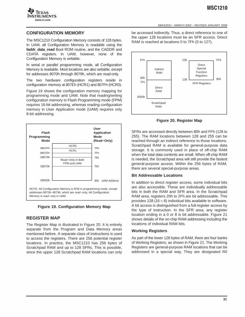
REGISTER MAPThe Register Map is illustrated in Figure 20. It is entirelyseparate from the Program and Data Memory areasmentioned before. A separate class of instructions is usedto access the registers. There are 256 potential registerlocations. In practice, the MSC1210 has 256 bytes ofScratchpad RAM and up to 128 SFRs. This is possible,since the upper 128 Scratchpad RAM locations can only
be accessed indirectly. Thus, a direct reference to one ofthe upper 128 locations must be an SFR access. DirectRAM is reached at locations 0 to 7Fh (0 to 127).
FFh 255
128
FFh
80h80h
7Fh
0000h
IndirectRAM
DirectRAM
ScratchpadRAM
SFR Registers
DirectSpecialFunctionRegisters
Figure 20. Register Map
SFRs are accessed directly between 80h and FFh (128 to255). The RAM locations between 128 and 255 can bereached through an indirect reference to those locations.Scratchpad RAM is available for general-purpose datastorage. It is commonly used in place of off-chip RAMwhen the total data contents are small. When off-chip RAMis needed, the Scratchpad area will still provide the fastestgeneral-purpose access. Within the 256 bytes of RAM,there are several special-purpose areas.
Bit Addressable Locations
In addition to direct register access, some individual bitsare also accessible. These are individually addressablebits in both the RAM and SFR area. In the ScratchpadRAM area, registers 20h to 2Fh are bit addressable. Thisprovides 128 (16 × 8) individual bits available to software.A bit access is distinguished from a full-register access bythe type of instruction. In the SFR area, any registerlocation ending in a 0 or 8 is bit addressable. Figure 21shows details of the on-chip RAM addressing including thelocations of individual RAM bits.
Working Registers
As part of the lower 128 bytes of RAM, there are four banksof Working Registers, as shown in Figure 21. The WorkingRegisters are general-purpose RAM locations that can beaddressed in a special way. They are designated R0

"#$%$&
SBAS203J − MARCH 2002 − REVISED JANUARY 2008
www.ti.com
32
through R7. Since there are four banks, the currentlyselected bank will be used by any instruction usingR0—R7. This allows software to change context by simplyswitching banks. This is controlled via the Program StatusWord register (PSW; 0D0h) in the SFR area describedbelow. Registers R0 and R1 also allow their contents to beused for indirect addressing of the upper 128 bytes ofRAM. Thus, an instruction can designate the value storedin R0 (for example) to address the upper RAM. The 16bytes immediately above the R0—R7 registers are bitaddressable; any of the 128 bits in this area can be directlyaccessed using bit addressable instructions.
FFh
7Fh
2Fh
2Dh
2Eh
2Ch
2Bh
2Ah
29h
28h
27h
26h
25h
24h
23h
22h
21h
20h
1Fh
18h17h
10h
0Fh
08h07h
7F 7E 7D 7C 7B 7A 79 78
77 76 75 74 73 72 71 70
6F 6E 6D 6C 6B 6A 69 68
67 66 65 64 63 62 61 60
5F 5E 5D 5C 5B 5A 59 58
57 56 55 54 53 52 51 50
4F 4E 4D 4C 4B 4A 49 48
47 46 45 44 43 42 41 40
3F 3E 3D 3C 3B 3A 39 38
37 36 35 34 33 32 31 30
2F 2E 2D 2C 2B 2A 29 28
27 26 25 24 23 22 21 20
1F 1E 1D 1C 1B 1A 19 18
17 16 15 14 13 12 11 10
0F 0E 0D 0C 0B 0A 09 08
07 06 05 04 03 02 01 00
0000h
DirectRAM
Bank 3
Bit
Add
ress
abl
e
Bank 2
Bank 1
Bank 0
MSB LSB
IndirectRAM
Figure 21. Scratchpad Register Addressing
Stack
Another use of the Scratchpad area is for theprogrammer’s stack. This area is selected using the StackPointer (SP; 81h) SFR. Whenever a call or interrupt isinvoked, the return address is placed on the Stack. It alsois available to the programmer for variables, etc., since theStack can be moved and there is no fixed location withinthe RAM designated as Stack. The Stack Pointer willdefault to 07h on reset. The user can then move it asneeded. A convenient location would be the upper RAMarea (> 7Fh) since this is only available indirectly. The SPwill point to the last used value. Therefore, the next valueplaced on the Stack is put at SP + 1. Each PUSH or CALLwill increment the SP by the appropriate value. Each POPor RET will decrement as well.
Program Memory
After reset, the CPU begins execution from ProgramMemory location 0000h. The selection of where ProgramMemory execution begins is made by tying the EA pin toDVDD for internal access, or DGND for external access.When EA is tied to DVDD, any PC fetches outside theinternal Program Memory address occur from externalmemory. If EA is tied to DGND, then all PC fetchesaddress external memory. The standard internal ProgramMemory size for MSC1210 family members is shown inTable 5. If enabled the Boot ROM will appear from addressF800h to FFFFh.
Table 5. MSC1210 Maximum Internal ProgramMemory Sizes
PRODUCTSTANDARD INTERNAL
PROGRAM MEMORY SIZE (BYTES)
MSC1210Y5 32k
MSC1210Y4 16k
MSC1210Y3 8k
MSC1210Y2 4k
Boot ROM
There is a 2kB Boot ROM that controls operation duringserial or parallel programming. The Boot ROM routinescan be accessed during the user mode if it is enabled. TheBoot ROM routines are listed in Table 6. When enabled,the Boot ROM routines will be located at memoryaddresses F800h−FFFFh during user mode. In programmode the Boot ROM is located in the first 2kB of ProgramMemory. For additional information, refer to ApplicationNote SBAA085, MSC1210 ROM Routines, available fordownload from the TI web site (www.ti.com).

"#$%$&
SBAS203J − MARCH 2002 − REVISED JANUARY 2008
www.ti.com
33
Table 6. MSC1210 Boot ROM Routines
ADDRESS ROUTINE C DECLARATIONS DESCRIPTION
FFD5 put_string void put_string (char code *string); Output string
FFD7 page_erase char page_erase (int faddr, char fdata, char fdm); Erase flash page
FFD9 write_flash Assembly only; DPTR = address, R5 = data Fast flash write
FFDB write_flash_chk char write_flash_chk (int faddr, char fdata, char fdm); Write flash byte, verify
FFDD write_flash_byte char write_flash_byte (int faddr, char fdata, char fdm); Write flash byte
FFDF faddr_data_read char faddr_data_read (char faddr); Read HW config byte from addr
FFE1 data_x_c_read char data_x_c_read (int faddr, char fdm); Read xdata or code byte
FFE3 tx_byte void tx_byte (char); Send byte to USART0
FFE5 tx_hex void tx_hex (char); Send hex value to USART0
FFE7 putok void putok (void); Send “OK” to USART0
FFE9 rx_byte char rx_byte (void); Read byte from USART0
FFEB rx_byte_echo char rx_byte_echo (void); Read and echo byte on USART0
FFED rx_hex_echo int rx_hex_echo (void); Read and echo hex on USART0
FFEF rx_hex_int_echo int rx_hex_int_echo (void); Read int as hex and echo: USART0
FFF1 rx_hex_rev_echo int rx_hex_rev_echo (void); Read int reversed as hex and echo: USART0
FFF3 autobaud void autobaud (void); Set baud rate with received CR
FFF5 putspace4 void putspace4 (void); Output 4 spaces to USART0
FFF7 putspace3 void putspace3 (void); Output 3 spaces to USART0
FFF9 putspace2 void putspace2 (void); Output 2 spaces to USART0
FFFB putspace1 void putspace1 (void); Output 1 space to USART0
FFFB putcr void putcr (void); Output CR, LF to USART0
F979 cmd_parse void cmd_parser (void); See SBAA076
FD37 monitor_isr void monitor_isr ( ) interrupt 6 Push registers and call cmd_parser

"#$%$&
SBAS203J − MARCH 2002 − REVISED JANUARY 2008
www.ti.com
34
ACCESSING EXTERNAL MEMORY
If external memory is used, P0 and P2 can be configuredas address and data lines. If external memory is not used,P0 and P2 can be configured as general-purpose I/O linesthrough the Hardware Configuration Register.
To enable access to external memory, bits 0 and 1 of theHCR1 register must be set to 0. When these bits areenabled all memory addresses for both internal andexternal memory will appear on ports 0 and 2. During thedata portion of the cycle for internal memory, Port 0 will bezero for security purposes.
Accesses to external memory are of two types: accessesto external Program Memory and accesses to externalData Memory. Accesses to external Program Memory usesignal PSEN (program store enable) as the read strobe.Accesses to external Data Memory use RD or WR(alternate functions of P3.7 and P3.6) to strobe thememory.
External Program Memory and external Data Memory maybe combined if desired by applying the RD and PSENsignals to the inputs of an AND gate and using the outputof the gate as the read strobe to the external Program/DataMemory.
Program fetches from external Program Memory alwaysuse a 16-bit address. Accesses to external Data Memorycan use either a 16-bit address (MOVX @DPTR) or an8-bit address (MOVX @RI).
If Port 2 is selected for external memory use (HCR1, bit 0),it cannot be used as general-purpose I/O. This bit (or Bit1 of HCR1) also forces bits P3.6 and P3.7 to be used forWR and RD instead of I/O. Port 2, P3.6, and P3.7 shouldall be written to ‘1.’
If an 8-bit address is being used (MOVX @RI), thecontents of the MPAGE (92h) SFR remain at the Port 2pins throughout the external memory cycle. This willfacilitate paging.
In any case, the low byte of the address is time-multiplexedwith the data byte on Port 0. The ADDR/DATA signals useCMOS drivers in the Port 0, Port 2, WR, and RD outputbuffers. Thus, in this application the Port 0 pins are notopen-drain outputs, and do not require external pull-ups forhigh-speed access. Signal ALE (Address Latch Enable)should be used to capture the address byte into an externallatch. The address byte is valid at the negative transitionof ALE. Then, in a write cycle, the data byte to be writtenappears on Port 0 just before WR is activated, and remainsthere until after WR is deactivated. In a read cycle, theincoming byte is accepted at Port 0 just before the readstrobe is deactivated.
The functions of Port 0 and Port 2 are selected in HardwareConfiguration Register 1. This can only be changed duringthe Flash Program mode. There is no conflict in the use ofthese registers; they will either be used asgeneral-purpose I/O or for external memory access. Thedefault state is for Port 0 and Port 2 to be used asgeneral-purpose I/O. If an external memory access isattempted when they are configured as general-purposeI/O, the values of Port 0 and Port 2 will not be affected.
External Program Memory is accessed under twoconditions:
1. Whenever signal EA is LOW during reset, then allfuture accesses are external; or
2. Whenever the Program Counter (PC) contains anumber that is outside of the internal ProgramMemory address range, if the ports are enabled.
If Port 0 and Port 2 are selected for external memory, all 8bits of Port 0 and Port 2, as well as P3.6 and P3.7, arededicated to an output function and may not be used forgeneral-purpose I/O. During external program fetches,Port 2 outputs the high byte of the PC.
Programming Flash Memory
There are four sections of Flash Memory for programming:
1. 128 configuration bytes.
2. Reset sector (4kB) (not to be confused with the 2kBBoot ROM).
3. Program Memory.
4. Data Memory.
Flash Programming Mode
There are two programming modes: parallel and serial. Theprogramming mode is selected by the state of the ALE andPSEN signals during power-on reset. Serial programmingmode is selected with PSEN = 0 and ALE = 1. Parallelprogramming mode is selected with PSEN = 1 and ALE = 0(see Figure 22). If they are both HIGH, the MSC1210 willoperate in normal user mode. Both signals LOW is areserved mode and is not defined. Programming mode isexited with a reset (BOR, WDT, software, or POR) and thenormal mode selected.

"#$%$&
SBAS203J − MARCH 2002 − REVISED JANUARY 2008
www.ti.com
35
PSEN
ALE
MSC1210 HOST
FlashProgrammer
P2[7]
P2[6:0]
P1[7:0]
P0[7:0]
P3[7:5]
P3[4]
P3[3]
P3[2]
RST
XIN
PSEL
AddrHi[6:0]
AddrLo[7:0]
Data[7:0]
Cmd[2:0]
Req
ACK
Pass
RST
CLK
NC
Figure 22. Parallel Programming Configuration
The MSC1210 is shipped with Flash Memory erased (all1s). Parallel programming methods typically involve athird-party programmer. Serial programming methodstypically involve in-system programming. UAM allowsFlash Program and Data Memory programming. Theactual code for Flash programming cannot execute fromFlash. That code must execute from the Boot ROM,internal (von Neumann) RAM or external memory.
Figure 23 shows the serial programming conection.
Serial programming mode works through USART0, andhas special protocols, which are discussed at length inApplication Note SBAA076, Programming the MSC1210,available for download at www.ti.com. The serialprogramming mode works at a maximum baud ratedetermined by fOSC.
MSC1210
PSEN
P3.0 RXD
P3.1 TXD
SerialPort 0
ALE
RSTAVDDDVDD
XIN
Reset Circuit
Clock Source
Not Connected
RS232Transceiver
Host PCor
Serial Terminal
NOTE: Serial programming is selected with PSEN = 0 and ALE = 1 or open.
Figure 23. Serial Programming Connection

"#$%$&
SBAS203J − MARCH 2002 − REVISED JANUARY 2008
www.ti.com
36
INTERRUPTS
The MSC1210 uses a three-priority interrupt system. Asshown in Table 7, each interrupt source has anindependent priority bit, flag, interrupt vector, and enable(except that nine interrupts share the Auxiliary Interrupt[AI] at the highest priority). In addition, interrupts can beglobally enabled or disabled. The interrupt structure iscompatible with the original 8051 family. All of the standardinterrupts are available.
HARDWARE CONFIGURATION MEMORY
The 128 configuration bytes can only be written during theprogram mode. The bytes are accessed through SFRregisters CADDR (SFR 93h) and CDATA (SFR 94h). Twoof the configuration bytes control Flash partitioning andsystem control. If the security bit is set, these bits can notbe changed except with a Mass Erase command thaterases all of the Flash Memory including the 128configuration bytes.
Table 7. Interrupt Summary
INTERRUPT PRIORITYINTERRUPT/EVENT ADDR NUM PRIORITY FLAG ENABLE
PRIORITYCONTROL
DVDD Low Voltage/HW Breakpoint 33h 6 HIGH EDLVB (AIE.0)(1)
EBP (BPCON.0)(1)
EDLVB (AIE.0)(1)
EBP (BPCON.0)(1)
N/A
AVDD Low Voltage 33h 6 0 EALV (AIE.1)(1) EALV (AIE.1)(1) N/A
SPI Receive 33h 6 0 ESPIR (AIE.2)(1) ESPIR (AIE.2)(1) N/A
SPI Transmit 33h 6 0 ESPIT (AIE.3)(1) ESPIT (AIE.3)(1) N/A
Milliseconds Timer 33h 6 0 EMSEC (AIE.4)(1) EMSEC (AIE.4)(1) N/A
ADC 33h 6 0 EADC (AIE.5)(1) EADC (AIE.5)(1) N/A
Summation Register 33h 6 0 ESUM (AIE.6)(1) ESUM (AIE.6)(1) N/A
Seconds Timer 33h 6 0 ESEC (AIE.7)(1) ESEC (AIE.7)(1) N/A
External Interrupt 0 03h 0 1 IE0 (TCON.1)(2) EX0 (IE.0)(4) PX0 (IP.0)
Timer 0 Overflow 0Bh 1 2 TF0 (TCON.5)(3) ET1 (IE.1)(4) PT0 (IP.1)
External Interrupt 1 13h 2 3 IE1 (TCON.3)(2) EX1 (IE.2)(4) PX1 (IP.2)
Timer 1 Overflow 0Bh 3 4 TF1 (TCON.7)(3) ET1 (IE.3)(4) PT1 (IP.3)
Serial Port 0 23h 4 5 RI_0 (SCON0.0)TI_0 (SCON0.1)
ES0 (IE.4)(4) PS0 (IP.4)
Timer 2 Overflow 2Bh 5 6 TF2 (T2CON.7) ET2 (IE.5)(4) PT2 (IP.5)
Serial Port 1 3Bh 7 7 RI_1 (SCON1.0)TI_1 (SCON1.1)
ES1 (IE.6)(4) PS1 (IP.6)
External Interrupt 2 43h 8 8 IE2 (EXIF.4) EX2 (EIE.0)(4) PX2 (EIP.0)
External Interrupt 3 4Bh 9 9 IE3 (EXIF.5) EX3 (EIE.1)(4) PX3 (EIP.1)
External Interrupt 4 53h 10 10 IE4 (EXIF.6) EX4 (EIE.2)(4) PX4 (EIP.2)
External Interrupt 5 5Bh 11 11 IE5 (EXIF.7) EX5 (EIE.3)(4) PX5 (EIP.3)
Watchdog 63h 12 12LOW
WDTI (EICON.3) EWDI (EIE.4)(4) PWDI (EIP.4)
(1) These interrupts set the AI flag (EICON.4) and are enabled by EAI (EICON.5).(2) If edge-triggered, cleared automatically by hardware when the service routine is vectored to. If level-triggered, the flag follows the state of the
pin.(3) Cleared automatically by hardware when interrupt vector occurs.(4) Globally enabled by EA (IE.7).

"#$%$&
SBAS203J − MARCH 2002 − REVISED JANUARY 2008
www.ti.com
37
Hardware Configuration Register 0 (HCR0)—Accessed Using SFR Registers CADDR and CDATA.
bit 7 bit 6 bit 5 bit 4 bit 3 bit 2 bit 1 bit 0
CADDR 7Fh EPMA PML RSL EBR EWDR DFSEL2 DFSEL1 DFSEL0
NOTE: HCR0 is programmable only in Flash Programming mode, but can be read in User Application mode using theCADDR and CDATA SFRs or the faddr_data_read Boot ROM routine.
EPMA Enable Programming Memory Access (Security Bit).bit 7 0: After reset in programming modes, Flash Memory can only be accessed in UAM until a mass erase is done.
1: Fully Accessible (default)
PML Program Memory Lock (PML has Priority Over RSL).bit 6 0: Enable all Flash Programming modes in program mode, can be written in UAM.
1: Enable read-only for program mode; cannot be written in UAM (default).
RSL Reset Sector Lock. The reset sector can be used to provide another method of Flash Memory programming. Thisbit 5 will allow Program Memory updates without changing the jumpers for in-circuit code updates or program
development. The code in this boot sector would then provide the monitor and programming routines with the abilityto jump into the main Flash code when programming is finished.0: Enable Reset Sector Writing1: Enable Read-Only Mode for Reset Sector (4kB) (default)
EBR Enable Boot ROM. Boot ROM is 2kB of code located in ROM, not to be confused with the 4kB Boot Sector locatedbit 4 in Flash Memory.
0: Disable Internal Boot ROM1: Enable Internal Boot ROM (default)
EWDR Enable Watchdog Reset.bit 3 0: Disable Watchdog Reset
1: Enable Watchdog Reset (default)
DFSEL Data Flash Memory Size (see Table 3 and Table 4).bits 2−0 000: Reserved
001: 32kB, 16kB, 8kB, or 4kB Data Flash Memory010: 16kB, 8kB, or 4kB Data Flash Memory011: 8kB or 4kB Data Flash Memory100: 4kB Data Flash Memory101: 2kB Data Flash Memory110: 1kB Data Flash Memory111: No Data Flash Memory (default)
"#$%$&
SBAS203J − MARCH 2002 − REVISED JANUARY 2008
www.ti.com
38
Hardware Configuration Register 1 (HCR1)
bit 7 bit 6 bit 5 bit 4 bit 3 bit 2 bit 1 bit 0
CADDR 7Eh DBLSEL1 DBLSEL0 ABLSEL1 ABLSEL0 DAB DDB EGP0 EGP23
NOTE: HCR1 is programmable only in Flash Programming mode, but can be read in User Application mode using theCADDR and CDATA SFRs or the faddr_data_read Boot ROM routine.
DBLSEL Digital Brownout Level Selectbits 7−6 00: 4.5V
01: 4.2V10: 2.7V11: 2.5V (default)
ABLSEL Analog Brownout Level Selectbits 5−4 00: 4.5V
01: 4.2V10: 2.7V11: 2.5V (default)
DAB Disable Analog Power-Supply Brownout Resetbit 3 0: Enable Analog Brownout Reset
1: Disable Analog Brownout Reset (default) (will not disable unless AVDD > 2.0V)
DDB Disable Digital Power-Supply Brownout Resetbit 2 0: Enable Digital Brownout Reset
1: Disable Digital Brownout Reset (default)
EGP0 Enable General-Purpose I/O for Port 0bit 1 0: Port 0 is Used for External Memory, P3.6 and P3.7 Used for WR and RD.
1: Port 0 is Used as General-Purpose I/O (default)
EGP23 Enable General-Purpose I/O for Ports 2 and 3bit 0 0: Port 2 is Used for External Memory, P3.6 and P3.7. Used for WR and RD.
1: Port 2 and Port3 are Used as General-Purpose I/O (default)
Configuration Memory Programming
Certain key functions such as Brownout Reset and Watchdog Timer are controlled by the hardware configuration bits.These bits are nonvolatile and can only be changed through serial and parallel programming. Other peripheral control andstatus functions, such as ADC configuration, timer setup, and Flash control, are controlled through the SFRs.

"#$%$&
SBAS203J − MARCH 2002 − REVISED JANUARY 2008
www.ti.com
39
SFR Definitions (Boldface definitions indicate that the register is unique to the MSC1210Yx)
ADDRESS REGISTER BIT 7 BIT 6 BIT 5 BIT 4 BIT 3 BIT 2 BIT 1 BIT 0 RESET VALUES
80h P0 P0.7 P0.6 P0.5 P0.4 P0.3 P0.2 P0.1 P0.0 FFh
81h SP 07h
82h DPL0 00h
83h DPH0 00h
84h DPL1 00h
85h DPH1 00h
86h DPS 0 0 0 0 0 0 0 SEL 00h
87h PCON SMOD 0 1 1 GF1 GF0 STOP IDLE 30h
88h TCON TF1 TR1 TF0 TR0 IE1 IT1 IE0 IT0 00h
89h TMOD −−−−−−−−−−−−−−− Timer 1 −−−−−−−−−−−−−−− −−−−−−−−−−−−−−− Timer 0 −−−−−−−−−−−−−−− 00h89h TMOD
GATE C/T M1 M0 GATE C/T M1 M0
00h
8Ah TL0 00h
8Bh TL1 00h
8Ch TH0 00h
8Dh TH1 00h
8Eh CKCON 0 0 T2M T1M T0M MD2 MD1 MD0 01h
8Fh MWS 0 0 0 0 0 0 0 MXWS 00h
90h P1 P1.7INT5/SCK
P1.6INT4/MISO
P1.5INT3/MOSI
P1.4INT2/SS
P1.3TXD1
P1.2RXD1
P1.1T2EX
P1.0T2
FFh
91h EXIF IE5 IE4 IE3 IE2 1 0 0 0 08h
92h MPAGE 00h
93h CADDR 00h
94h CDATA 00h
95h MCON BPSEL 0 0 RAMMAP 00h
96h
97h
98h SCON0 SM0_0 SM1_0 SM2_0 REN_0 TB8_0 RB8_0 TI_0 RI_0 00h
99h SBUF0 00h
9Ah SPICON SCK2 SCK1 SCK0 0 ORDER MSTR CPHA CPOL 00h
9Bh SPIDATA 00h
9Dh SPITCON CLK_EN DRV_DLY DRV_EN 00h
A0h P2 P2.7 P2.6 P2.5 P2.4 P2.3 P2.2 P2.1 P2.0 FFh
A1h PWMCON PPOL PWMSEL SPDSEL TPCNTL2 TPCNTL1 TPCNTL0 00h
A2h PWMLOWTONELOW
PWM7TDIV7
PWM6TDIV6
PWM5TDIV5
PWM4TDIV4
PWM3TDIV3
PWM2TDIV2
PWM1TDIV1
PWM0TDIV0
00h
A3h PWMHITONEHI
PWM15TDIV15
PWM14TDIV14
PWM13TDIV13
PWM12TDIV12
PWM11TDIV11
PWM10TDIV10
PWM9TDIV9
PWM8TDIV8
00h
A4h
A5h PAI 0 0 0 0 PAI3 PAI2 PAI1 PAI0 00h
A6h AIE ESEC ESUM EADC EMSEC ESPIT ESPIR EALV EDLVB 00h
A7h AISTAT SEC SUM ADC MSEC SPIT SPIR ALVD DLVD 00h
A8h IE EA ES1 ET2 ES0 ET1 EX1 ET0 EX0 00h
A9h BPCON BP 0 0 0 0 0 PMSEL EBP 00h
AAh BPL 00h
ABh BPH 00h
ACh P0DDRL P03H P03L P02H P02L P01H P01L P00H P00L 00h
ADh P0DDRH P07H P07L P06H P06L P05H P05L P04H P04L 00h

"#$%$&
SBAS203J − MARCH 2002 − REVISED JANUARY 2008
www.ti.com
40
SFR Definitions (continued) (Boldface definitions indicate that the register is unique to the MSC1210Yx)
ADDRESS RESET VALUESBIT 0BIT 1BIT 2BIT 3BIT 4BIT 5BIT 6BIT 7REGISTER
AEh P1DDRL P13H P13L P12H P12L P11H P11L P10H P10L 00h
AFh P1DDRH P17H P17L P16H P16L P15H P15L P14H P14L 00h
B0h P3 P3.7RD
P3.6WR
P3.5T1
P3.4T0
P3.3INT1
P3.2INT0
P3.1TXD0
P3.0RXD0
FFh
B1h P2DDRL P23H P23L P22H P22L P21H P21L P20H P20L 00h
B2h P2DDRH P27H P27L P26H P26L P25H P25L P24H P24L 00h
B3h P3DDRL P33H P33L P32H P32L P31H P31L P30H P30L 00h
B4h P3DDRH P37H P37L P36H P36L P35H P35L P34H P34L 00h
B5h
B6h
B7h
B8h IP 1 PS1 PT2 PS0 PT1 PX1 PT0 PX0 80h
B9h
BAh
BBh
BCh
BDh
BEh
BFh
C0h SCON1 SM0_1 SM1_1 SM2_1 REN_1 TB8_1 RB8_1 TI_1 RI_1 00h
C1h SBUF1 00h
C2h
C3h
C4h
C5h
C6h EWU EWUWDT EWUEX1 EWUEX0 00h
C7h
C8h T2CON TF2 EXF2 RCLK TCLK EXEN2 TR2 C/T2 CP/RL2 00h
C9h
CAh RCAP2L 00h
CBh RCAP2H 00h
CCh TL2 00h
CDh TH2 00h
CEh
CFh
D0h PSW CY AC F0 RS1 RS0 OV F1 P 00h
D1h OCL LSB 00h
D2h OCM 00h
D3h OCH MSB 00h
D4h GCL LSB 5Ah
D5h GCM ECh
D6h GCH MSB 5Fh
D7h ADMUX INP3 INP2 INP1 INP0 INN3 INN2 INN1 INN0 01h
D8h EICON SMOD1 1 EAI AI WDTI 0 0 0 40h
D9h ADRESL LSB 00h
DAh ADRESM 00h

"#$%$&
SBAS203J − MARCH 2002 − REVISED JANUARY 2008
www.ti.com
41
SFR Definitions (continued) (Boldface definitions indicate that the register is unique to the MSC1210Yx)
ADDRESS RESET VALUESBIT 0BIT 1BIT 2BIT 3BIT 4BIT 5BIT 6BIT 7REGISTER
DBh ADRESH MSB 00h
DCh ADCON0 — BOD EVREF VREFH EBUF PGA2 PGA1 PGA0 30h
DDh ADCON1 — POL SM1 SM0 — CAL2 CAL1 CAL0 0000_0000b
DEh ADCON2 DR7 DR6 DR5 DR4 DR3 DR2 DR1 DR0 1Bh
DFh ADCON3 0 0 0 0 0 DR10 DR9 DR8 06h
E0h ACC 00h
E1h SSCON SSCON1 SSCON0 SCNT2 SCNT1 SCNT0 SHF2 SHF1 SHF0 00h
E2h SUMR0 00h
E3h SUMR1 00h
E4h SUMR2 00h
E5h SUMR3 00h
E6h ODAC 00h
E7h LVDCON ALVDIS ALVD2 ALVD1 ALVD0 DLVDIS DLVD2 DLVD1 DLVD0 00h
E8h EIE 1 1 1 EWDI EX5 EX4 EX3 EX2 E0h
E9h HWPC0 0 0 0 0 0 0 MEMORY SIZE 0000_00xxb
EAh HWPC1 0 0 0 0 0 0 0 0 00h
EBh HDWVER xxh
ECh Reserved 00h
EDh Reserved 00h
EEh FMCON 0 PGERA 0 FRCM 0 BUSY 1 0 02h
EFh FTCON FER3 FER2 FER1 FER0 FWR3 FWR2 FWR1 FWR0 A5h
F0h B B.7 B.6 B.5 B.4 B.3 B.2 B.1 B.0 00h
F1h PDCON 0 0 0 PDPWM PDADC PDWDT PDST PDSPI 1Fh
F2h PASEL 0 0 PSEN2 PSEN1 PSEN0 0 ALE1 ALE0 00h
F3h
F4h
F5h
F6h ACLK 0 FREQ6 FREQ5 FREQ4 FREQ3 FREQ2 FREQ1 FREQ0 03h
F7h SRST 0 0 0 0 0 0 0 RSTREQ 00h
F8h EIP 1 1 1 PWDI PX5 PX4 PX3 PX2 E0h
F9h SECINT WRT SECINT6 SECINT5 SECINT4 SECINT3 SECINT2 SECINT1 SECINT0 7Fh
FAh MSINT WRT MSINT6 MSINT5 MSINT4 MSINT3 MSINT2 MSINT1 MSINT0 7Fh
FBh USEC 0 0 0 FREQ4 FREQ3 FREQ2 FREQ1 FREQ0 03h
FCh MSECL 9Fh
FDh MSECH 0Fh
FEh HMSEC 63h
FFh WDTCON EWDT DWDT RWDT WDCNT4 WDCNT3 WDCNT2 WDCNT1 WDCNT0 00h

"#$%$&
SBAS203J − MARCH 2002 − REVISED JANUARY 2008
www.ti.com
42
Table 8. Special Function Register Cross Reference
SFR ADDRESS FUNCTIONS CPU INTERRUPTS PORTSSERIALCOMM.
POWERAND
CLOCKSTIMER
COUNTERS PWMFLASH
MEMORY ADC
P0 80h Port 0 X
SP 81h Stack Pointer X
DPL0 82h Data Pointer Low 0 X
DPH0 83h Data Pointer High 0 X
DPL1 84h Data Pointer Low 1 X
DPH1 85h Data Pointer High 1 X
DPS 86h Data Pointer Select X
PCON 87h Power Control X
TCON 88h Timer/Counter Control X X
TMOD 89h Timer Mode Control X X
TL0 8Ah Timer0 LSB X
TL1 8Bh Timer1 LSB X
TH0 8Ch Timer0 MSB X
TH1 8Dh Timer1 MSB X
CKCON 8Eh Clock Control X X X
MWS 8Fh Memory Write Select X
P1 90h Port 1 X
EXIF 91h External Interrupt Flag X
MPAGE 92h Memory Page X
CADDR 93h Configuration Address X
CDATA 94h Configuration Data X
MCON 95h Memory Control X
SCON0 98h Serial Port 0 Control X X
SBUF0 99h Serial Data Buffer 0 X
SPICON9Ah
SPI Control X
I2CCON9Ah
I2C Control X
SPIDATA9Bh
SPI Data X
I2CDATA9Bh
I2C Data X
SPITCON9Dh
SPI Transmit Control X
I2CSTAT9Dh
I2C Status X
P2 A0h Port 2 X
PWMCON A1h PWM Control X X
PWMLOWA2h
PWM Low Byte X
TONELOWA2h
Tone Low Byte X
PWMHIA3h
PWM HIgh Byte X
TONEHIA3h
Tone Low Byte X
PAI A5h Pending Auxiliary Interrupt X X X X X X
AIE A6h Auxiliary Interrupt Enable X X X X X X
AISTAT A7h Auxiliary Interrupt Status X X X X X X
IE A8h Interrupt Enable X
BPCON A9h Breakpoint Control X X
BPL AAh Breakpoint Low Address X X
BPH ABh Breakpoint High Address X X
P0DDRL ACh Port 0 Data Direction Low X
P0DDRH ADh Port 0 Data Direction High X
P1DDRL AEh Port 1 Data Direction Low X
P1DDRH AFh Port 1 Data Direction High X
P3 B0h Port 3 X
"#$%$&
SBAS203J − MARCH 2002 − REVISED JANUARY 2008
www.ti.com
43
Table 8. Special Function Register Cross Reference (continued)
SFR ADCFLASH
MEMORYPWMTIMER
COUNTERS
POWERAND
CLOCKSSERIALCOMM.PORTSINTERRUPTSCPUFUNCTIONSADDRESS
P2DDRL B1h Port 2 Data Direction Low X
P2DDRH B2h Port 2 Data Direction High X
P3DDRL B3h Port 3 Data Direction Low X
P3DDRH B4h Port 3 Data Direction High X
IP B8h Interrupt Priority X
SCON1 C0h Serial Port 1 Control X X
SBUF1 C1h Serial Data Buffer 1 X
EWU C6h Enable Wake Up X X
T2CON C8h Timer 2 Control X X
RCAP2L CAh Timer 2 Capture LSB X X
RCAP2H CBh Timer 2 Capture MSB X X
TL2 CCh Timer 2 LSB X
TH2 CDh Timer 2 MSB X
PSW D0h Program Status Word X
OCL D1h ADC Offset Calibration Low Byte X
OCM D2h ADC Offset Calibration Mid Byte X
OCH D3h ADC Offset Calibration High Byte X
GCL D4h ADC Gain Calibration Low Byte X
GCM D5h ADC Gain Calibration Mid Byte X
GCH D6h ADC Gain Calibration High Byte X
ADMUX D7h ADC Input Multiplexer X
EICON D8h Enable Interrupt Control X X X X
ADRESL D9h ADC Results Low Byte X
ADRESM DAh ADC Results Middle Byte X
ADRESH DBh ADC Results High Byte X
ADCON0 DCh ADC Control 0 X
ADCON1 DDh ADC Control 1 X
ADCON2 DEh ADC Control 2 X
ADCON3 DFh ADC Control 3 X
ACC E0h Accumulator X
SSCON E1h Summation/Shifter Control X X
SUMR0 E2h Summation 0 X X
SUMR1 E3h Summation 1 X X
SUMR2 E4h Summation 2 X X
SUMR3 E5h Summation 3 X X
ODAC E6h Offset DAC X
LVDCON E7h Low Voltage Detect Control X
EIE E8h Extended Interrupt Enable X
HWPC0 E9h Hardware Product Code 0 X
HWPC1 EAh Hardware Product Code 1 X
HWVER EBh Hardware Version X
FMCON EEh Flash Memory Control X
FTCON EFh Flash Memory Timing Control X

"#$%$&
SBAS203J − MARCH 2002 − REVISED JANUARY 2008
www.ti.com
44
Table 8. Special Function Register Cross Reference (continued)
SFR ADCFLASH
MEMORYPWMTIMER
COUNTERS
POWERAND
CLOCKSSERIALCOMM.PORTSINTERRUPTSCPUFUNCTIONSADDRESS
B F0h Second Accumulator X
PDCON F1h Power Down Control X X X X
PASEL F2h PSEN/ALE Select X X
ACLK F6h Analog Clock X X
SRST F7h System Reset X X
EIP F8h Extended Interrupt Priority X
SECINT F9h Seconds Timer Interrupt X X
MSINT FAh Milliseconds Timer Interrupt X X
USEC FBh One Microsecond TImer X X X
MSECL FCh One Millisecond TImer Low Byte X X
MSECH FDh One Millisecond Timer High Byte X X
HMSEC FEh One Hundred Millisecond TImer X
WDTCON FFh Watchdog Timer X X
HCR0 3Fh Hardware Configuration Reg. 0 X
HCR1 3Eh Hardware Configuration Reg. 1 X
"#$%$&
SBAS203J − MARCH 2002 − REVISED JANUARY 2008
www.ti.com
45
Port 0 (P0)
7 6 5 4 3 2 1 0 Reset Value
SFR 80h P0.7 P0.6 P0.5 P0.4 P0.3 P0.2 P0.1 P0.0 FFh
P0.7−0 Port 0. This port functions as a multiplexed address/data bus during external memory access, and as a general-bits 7−0 purpose I/O port when external memory access is not needed. During external memory cycles, this port will contain
the LSB of the address when ALE is HIGH, and Data when ALE is LOW. When used as a general-purpose I/O, thisport drive is selected by P0DDRL and P0DDRH (ACh, ADh). Whether Port 0 is used as general-purpose I/O or forexternal memory access is determined by the Flash Configuration Register (HCR1.1)
Stack Pointer (SP)
7 6 5 4 3 2 1 0 Reset Value
SFR 81h SP.7 SP.6 SP.5 SP.4 SP.3 SP.2 SP.1 SP.0 07h
SP.7−0 Stack Pointer. The stack pointer identifies the location where the stack will begin. The stack pointer is incrementedbits 7−0 before every PUSH or CALL operation and decremented after each POP or RET/RETI. This register defaults to 07h
after reset.
Data Pointer Low 0 (DPL0)
7 6 5 4 3 2 1 0 Reset Value
SFR 82h DPL0.7 DPL0.6 DPL0.5 DPL0.4 DPL0.3 DPL0.2 DPL0.1 DPL0.0 00h
DPL0.7−0 Data Pointer Low 0. This register is the low byte of the standard 8051 16-bit data pointer. DPL0 and DPH0 arebits 7−0 used to point to non-scratchpad data RAM. The current data pointer is selected by DPS (SFR 86h).
Data Pointer High 0 (DPH0)
7 6 5 4 3 2 1 0 Reset Value
SFR 83h DPH0.7 DPH0.6 DPH0.5 DPH0.4 DPH0.3 DPH0.2 DPH0.1 DPH0.0 00h
DPH0.7−0 Data Pointer High 0. This register is the high byte of the standard 8051 16-bit data pointer. DPL0 and DPH0 arebits 7−0 used to point to non-scratchpad data RAM. The current data pointer is selected by DPS (SFR 86h).
Data Pointer Low 1 (DPL1)
7 6 5 4 3 2 1 0 Reset Value
SFR 84h DPL1.7 DPL1.6 DPL1.5 DPL1.4 DPL1.3 DPL1.2 DPL1.1 DPL1.0 00h
DPL1.7−0 Data Pointer Low 1. This register is the low byte of the auxiliary 16-bit data pointer. When the SEL bit (DPS.0,bits 7−0 SFR 86h) is set, DPL1 and DPH1 are used in place of DPL0 and DPH0 during DPTR operations.

"#$%$&
SBAS203J − MARCH 2002 − REVISED JANUARY 2008
www.ti.com
46
Data Pointer High 1 (DPH1)
7 6 5 4 3 2 1 0 Reset Value
SFR 85h DPH1.7 DPH1.6 DPH1.5 DPH1.4 DPH1.3 DPH1.2 DPH1.1 DPH1.0 00h
DPH1.7−0 Data Pointer High. This register is the high byte of the auxiliary 16-bit data pointer. When the SEL bit (DPS.0,bits 7−0 SFR 86h) is set, DPL1 and DPH1 are used in place of DPL0 and DPH0 during DPTR operations.
Data Pointer Select (DPS)
7 6 5 4 3 2 1 0 Reset Value
SFR 86h 0 0 0 0 0 0 0 SEL 00h
SEL Data Pointer Select. This bit selects the active data pointer.bit 0 0: Instructions that use the DPTR will use DPL0 and DPH0.
1: Instructions that use the DPTR will use DPL1 and DPH1.
Power Control (PCON)
7 6 5 4 3 2 1 0 Reset Value
SFR 87h SMOD 0 1 1 GF1 GF0 STOP IDLE 30h
SMOD Serial Port 0 Baud Rate Doubler Enable. The serial baud rate doubling function for Serial Port 0.bit 7 0: Serial Port 0 baud rate will be a standard baud rate.
1: Serial Port 0 baud rate will be double that defined by baud rate generation equation when using Timer 1.
GF1 General-Purpose User Flag 1. This is a general-purpose flag for software control.bit 3
GF0 General-Purpose User Flag 0. This is a general-purpose flag for software control.bit 2
STOP Stop Mode Select. Setting this bit will halt the oscillator and block external clocks. This bit will always read as a 0.bit 1 All DACs and digital pins keep their respective output values. Exit with RESET.
IDLE Idle Mode Select. Setting this bit will freeze the CPU, Timer 0, 1, and 2, and the USARTs; other peripherals remainbit 0 active. All DACs and digital pins keep their respective output values. This bit will always be read as a 0. Exit with AI
(A6h) and EWU (C6h) interrupts.The internal reference remains unchanged.

"#$%$&
SBAS203J − MARCH 2002 − REVISED JANUARY 2008
www.ti.com
47
Timer/Counter Control (TCON)
7 6 5 4 3 2 1 0 Reset Value
SFR 88h TF1 TR1 TF0 TR0 IE1 IT1 IE0 IT0 00h
TF1 Timer 1 Overflow Flag. This bit indicates when Timer 1 overflows its maximum count as defined by the current mode.bit 7 This bit can be cleared by software and is automatically cleared when the CPU vectors to the Timer 1 interrupt service
routine.0: No Timer 1 overflow has been detected.1: Timer 1 has overflowed its maximum count.
TR1 Timer 1 Run Control. This bit enables/disables the operation of Timer 1. Halting this timer will preserve the current countbit 6 in TH1, TL1.
0: Timer is halted.1: Timer is enabled.
TF0 Timer 0 Overflow Flag. This bit indicates when Timer 0 overflows its maximum count as defined by the current mode.bit 5 This bit can be cleared by software and is automatically cleared when the CPU vectors to the Timer 0 interrupt service
routine.0: No Timer 0 overflow has been detected.1: Timer 0 has overflowed its maximum count.
TR0 Timer 0 Run Control. This bit enables/disables the operation of Timer 0. Halting this timer will preserve the currentbit 4 count in TH0, TL0.
0: Timer is halted.1: Timer is enabled.
IE1 Interrupt 1 Edge Detect. This bit is set when an edge/level of the type defined by IT1 is detected. If IT1 = 1, this bitbit 3 will remain set until cleared in software or the start of the External Interrupt 1 service routine. If IT1 = 0, this bit will
inversely reflect the state of the INT1 pin.
IT1 Interrupt 1 Type Select. This bit selects whether the INT1 pin will detect edge or level triggered interrupts.bit 2 0: INT1 is level triggered.
1: INT1 is edge triggered.
IE0 Interrupt 0 Edge Detect. This bit is set when an edge/level of the type defined by IT0 is detected. If IT0 = 1, this bitbit 3 will remain set until cleared in software or the start of the External Interrupt 0 service routine. If IT0 = 0, this bit will
inversely reflect the state of the INT0 pin.
IT0 Interrupt 0 Type Select. This bit selects whether the INT0 pin will detect edge or level triggered interrupts.bit 2 0: INT0 is level triggered.
1: INT0 is edge triggered.
"#$%$&
SBAS203J − MARCH 2002 − REVISED JANUARY 2008
www.ti.com
48
Timer Mode Control (TMOD)
7 6 5 4 3 2 1 0
TIMER 1 TIMER 0 Reset ValueSFR 89h GATE C/T M1 M0 GATE C/T M1 M0
Reset Value00h
GATE Timer 1 Gate Control. This bit enables/disables the ability of Timer 1 to increment.bit 7 0: Timer 1 will clock when TR1 = 1, regardless of the state of pin INT1.
1: Timer 1 will clock only when TR1 = 1 and pin INT1 = 1.
C/T Timer 1 Counter/Timer Select.bit 6 0: Timer is incremented by internal clocks.
1: Timer is incremented by pulses on T1 pin when TR1 (TCON.6, SFR 88h) is 1.
M1, M0 Timer 1 Mode Select. These bits select the operating mode of Timer 1.bits 5−4
M1 M0 MODE
0 0 Mode 0: 8-bit counter with 5-bit prescale.
0 1 Mode 1: 16 bits.
1 0 Mode 2: 8-bit counter with auto reload.
1 1 Mode 3: Timer 1 is halted, but holds its count.
GATE Timer 0 Gate Control. This bit enables/disables the ability of Timer 0 to increment.bit 3 0: Timer 0 will clock when TR0 = 1, regardless of the state of pin INT0 (software control).
1: Timer 0 will clock only when TR0 = 1 and pin INT0 = 1 (hardware control).
C/T Timer 0 Counter/Timer Select.bit 2 0: Timer is incremented by internal clocks.
1: Timer is incremented by pulses on pin T0 when TR0 (TCON.4, SFR 88h) is 1.
M1, M0 Timer 0 Mode Select. These bits select the operating mode of Timer 0.bits 1−0
M1 M0 MODE
0 0 Mode 0: 8-bit counter with 5-bit prescale.
0 1 Mode 1: 16 bits.
1 0 Mode 2: 8-bit counter with auto reload.
1 1 Mode 3: Two 8-bit counters.
Timer 0 LSB (TL0)
7 6 5 4 3 2 1 0 Reset Value
SFR 8Ah TL0.7 TL0.6 TL0.5 TL0.4 TL0.3 TL0.2 TL0.1 TL0.0 00h
TL0.7−0 Timer 0 LSB. This register contains the least significant byte of Timer 0.bits 7−0
Timer 1 LSB (TL1)
7 6 5 4 3 2 1 0 Reset Value
SFR 8Bh TL1.7 TL1.6 TL1.5 TL1.4 TL1.3 TL1.2 TL1.1 TL1.0 00h
TL1.7−0 Timer 1 LSB. This register contains the least significant byte of Timer 1.bits 7−0

"#$%$&
SBAS203J − MARCH 2002 − REVISED JANUARY 2008
www.ti.com
49
Timer 0 MSB (TH0)
7 6 5 4 3 2 1 0 Reset Value
SFR 8Ch TH0.7 TH0.6 TH0.5 TH0.4 TH0.3 TH0.2 TH0.1 TH0.0 00h
TH0.7−0 Timer 0 MSB. This register contains the most significant byte of Timer 0.bits 7−0
Timer 1 MSB (TH1)
7 6 5 4 3 2 1 0 Reset Value
SFR 8Dh TH1.7 TH1.6 TH1.5 TH1.4 TH1.3 TH1.2 TH1.1 TH1.0 00h
TH1.7−0 Timer 1 MSB. This register contains the most significant byte of Timer 1.bits 7−0
Clock Control (CKCON)
7 6 5 4 3 2 1 0 Reset Value
SFR 8Eh 0 0 T2M T1M T0M MD2 MD1 MD0 01h
T2M Timer 2 Clock Select. This bit controls the division of the system clock that drives Timer 2. This bit has no effect whenbit 5 the timer is in baud rate generator or clock output mode. Clearing this bit to 0 maintains 8051 compatibility. This bit
has no effect on instruction cycle timing.0: Timer 2 uses a divide-by-12 of the crystal frequency.1: Timer 2 uses a divide-by-4 of the crystal frequency.
T1M Timer 1 Clock Select. This bit controls the division of the system clock that drives Timer 1. Clearing this bit to 0bit 4 maintains 8051 compatibility. This bit has no effect on instruction cycle timing.
0: Timer 1 uses a divide-by-12 of the crystal frequency.1: Timer 1 uses a divide-by-4 of the crystal frequency.
T0M Timer 0 Clock Select. This bit controls the division of the system clock that drives Timer 0. Clearing this bit to 0bit 3 maintains 8051 compatibility. This bit has no effect on instruction cycle timing.
0: Timer 0 uses a divide-by-12 of the crystal frequency.1: Timer 0 uses a divide-by-4 of the crystal frequency.
MD2, MD1, MD0 Stretch MOVX Select 2−0. These bits select the time by which external MOVX cycles are to be stretched. Thisbits 2−0 allows slower memory or peripherals to be accessed without using ports or manual software intervention. The
width of the RD or WR strobe will be stretched by the specified interval, which will be transparent to the softwareexcept for the increased time to execute the MOVX instruction. All internal MOVX instructions on devicescontaining MOVX SRAM are performed at the 2 instruction cycle rate.
MD2 MD1 MD0STRETCH
VALUE MOVX DURATIONRD or WR STROBE WIDTH
(SYS CLKs)RD or WR STROBE WIDTH
(s) at 12MHz
0 0 0 0 2 Instruction Cycles 2 0.167
0 0 1 1 3 Instruction Cycles (default)(1) 4 0.333
0 1 0 2 4 Instruction Cycles 8 0.667
0 1 1 3 5 Instruction Cycles 12 1.000
1 0 0 4 6 Instruction Cycles 16 1.333
1 0 1 5 7 Instruction Cycles 20 1.667
1 1 0 6 8 Instruction Cycles 24 2.000
1 1 1 7 9 Instruction Cycles 28 2.333
(1) For applications without external memory, no extra cycle is needed. To increase speed, set MD2, MD1, and MD0 to ‘000’.
"#$%$&
SBAS203J − MARCH 2002 − REVISED JANUARY 2008
www.ti.com
50
Memory Write Select (MWS)
7 6 5 4 3 2 1 0 Reset Value
SFR 8Fh 0 0 0 0 0 0 0 MXWS 00h
MXWS MOVX Write Select. This allows writing to the internal Flash program memory.bit 0 0: No writes are allowed to the internal Flash program memory.
1: Writing is allowed to the internal Flash program memory, unless PML (HCR0) or RSL (HCR0) are on.
Port 1 (P1)
7 6 5 4 3 2 1 0 Reset Value
SFR 90hP1.7
INT5/SCKP1.6
INT4/MISOP1.5
INT3/MOSIP1.4
INT2/SSP1.3TXD1
P1.2RXD1
P1.1T2EX
P1.0T2
FFh
P1.7−0 General-Purpose I/O Port 1. This register functions as a general-purpose I/O port. In addition, all the pins have anbits 7−0 alternative function listed below. Each of the functions is controlled by several other SFRs. The associated Port 1
latch bit must contain a logic ‘1’ before the pin can be used in its alternate function capacity. To use the alternatefunction, set the appropriate mode in P1DDRL (SFR AEh), P1DDRH (SFR AFh).
INT5/SCK External Interrupt 5. A falling edge on this pin will cause an external interrupt 5 if enabled.bit 7 SPI Clock. The master clock for SPI data transfers.
INT4/MISO External Interrupt 4. A rising edge on this pin will cause an external interrupt 4 if enabled.bit 6 Master In Slave Out. For SPI data transfers, this pin receives data for the master and transmits data from the slave.
INT3/MOSI External Interrupt 3. A falling edge on this pin will cause an external interrupt 3 if enabled.bit 5 Master Out Slave In. For SPI data transfers, this pin transmits master data and receives slave data.
INT2/SS External Interrupt 2. A rising edge on this pin will cause an external interrupt 2 if enabled.bit 4 Slave Select. During SPI operation, this pin provides the select signal for the slave device but does not control the
output drive of MISO.
TXD1 Serial Port 1 Transmit. This pin transmits the serial Port 1 data in serial port modes 1, 2, 3, and emits the synchro-bit 3 nizing clock in serial port mode 0.
RXD1 Serial Port 1 Receive. This pin receives the serial Port 1 data in serial port modes 1, 2, 3, and is a bidirectional databit 2 transfer pin in serial port mode 0.
T2EX Timer 2 Capture/Reload Trigger. A 1 to 0 transition on this pin will cause the value in the T2 registers to bebit 1 transferred into the capture registers, if enabled by EXEN2 (T2CON.3, SFR C8h). When in auto-reload mode, a 1
to 0 transition on this pin will reload the Timer 2 registers with the value in RCAP2L and RCAP2H if enabled by EXEN2(T2CON.3, SFR C8h).
T2 Timer 2 External Input. A 1 to 0 transition on this pin will cause Timer 2 to increment.bit 0
"#$%$&
SBAS203J − MARCH 2002 − REVISED JANUARY 2008
www.ti.com
51
External Interrupt Flag (EXIF)
7 6 5 4 3 2 1 0 Reset Value
SFR 91h IE5 IE4 IE3 IE2 1 0 0 0 08h
IE5 External Interrupt 5 Flag. This bit will be set when a falling edge is detected on INT5. This bit must be clearedbit 7 manually by software. Setting this bit in software will cause an interrupt if enabled.
IE4 External Interrupt 4 Flag. This bit will be set when a rising edge is detected on INT4. This bit must be clearedbit 6 manually by software. Setting this bit in software will cause an interrupt if enabled.
IE3 External Interrupt 3 Flag. This bit will be set when a falling edge is detected on INT3. This bit must be clearedbit 5 manually by software. Setting this bit in software will cause an interrupt if enabled.
IE2 External Interrupt 2 Flag. This bit will be set when a rising edge is detected on INT2. This bit must be clearedbit 4 manually by software. Setting this bit in software will cause an interrupt if enabled.
Memory Page (MPAGE)
7 6 5 4 3 2 1 0 Reset Value
SFR 92h 00h
MPAGE The 8051 uses Port 2 for the upper 8 bits of the external data memory access by MOVX A,@Ri and MOVX @Ri,Abits 7−0 instructions. The MSC1210 uses register MPAGE instead of Port 2. To access external data memory using the MOVX
A,@Ri and MOVX @Ri,A instructions, the user should preload the upper byte of the address into MPAGE (versuspreloading into P2 for the standard 8051).
Configuration Address Register (CADDR) (write-only)
7 6 5 4 3 2 1 0 Reset Value
SFR 93h 00h
CADDR Configuration Address Register. This register supplies the address for reading bytes in the 128 bytes of Flashbits 7−0 Configuration memory. This is a write-only register.
CAUTION: If this register is written to while executing from Flash Memory, the CDATA register will be incorrect.The faddr_data_read routine in the Boot ROM can be used for this purpose.
Configuration Data Register (CDATA) (read-only)
7 6 5 4 3 2 1 0 Reset Value
SFR 94h 00h
CDATA Configuration Data Register. This register will contain the data in the 128 bytes of Flash Configuration memory thatbits 7−0 are located at the last written address in the CADDR register. This is a read-only register.

"#$%$&
SBAS203J − MARCH 2002 − REVISED JANUARY 2008
www.ti.com
52
Memory Control (MCON)
7 6 5 4 3 2 1 0 Reset Value
SFR 95h BPSEL 0 0 — — — — RAMMAP 00h
BPSEL Breakpoint Address Selectionbit 7 Write: Select one of two Breakpoint registers: 0 or 1.
0: Select breakpoint register 0.1: Select breakpoint register 1.Read: Provides the Breakpoint register that created the last interrupt: 0 or 1.
RAMMAP Memory Map 1kB extended SRAM.bit 0 0: Address is: 0000h—03FFh (default) (Data Memory)
1: Address is 8400h—87FFh (Data and Program Memory)
Serial Port 0 Control (SCON0)
7 6 5 4 3 2 1 0 Reset Value
SFR 98h SM0_0 SM1_0 SM2_0 REN_0 TB8_0 RB8_0 TI_0 RI_0 00h
SM0−2 Serial Port 0 Mode. These bits control the mode of serial Port 0. Modes 1, 2, and 3 have 1 start and 1 stop bit inbits 7−5 addition to the 8 or 9 data bits.
MODE SM0 SM1 SM2 FUNCTION LENGTH PERIOD
0 0 0 0 Synchronous 8 bits 12 pCLK(1)
0 0 0 1 Synchronous 8 bits 4 pCLK(1)
1(2) 0 1 0 Asynchronous 10 bits Timer 1 or 2 Baud Rate Equation1(2) 0 1 1 Valid Stop Required(3) 10 bits Timer 1 Baud Rate Equation
2 1 0 0 Asynchronous 11 bits 64 pCLK(1) (SMOD = 0)32 pCLK(1) (SMOD = 1)
2 1 0 1 Asynchronous with Multiprocessor Communication(4) 11 bits 64 pCLK(1) (SMOD = 0)32 pCLK(1) (SMOD = 1)
3(2) 1 1 0 Asynchronous 11 bits Timer 1 or 2 Baud Rate Equation3(2) 1 1 1 Asynchronous with Multiprocessor Communication(4) 11 bits Timer 1 or 2 Baud Rate Equation
(1) pCLK will be equal to tCLK, except that pCLK will stop for IDLE.(2) For modes 1 and 3, the selection of Timer 1 or 2 for baud rate is specified via the T2CON (C8h) register.(3) RI_0 will only be activated when a valid STOP is received.(4) RI_0 will not be activated if bit 9 = 0.
REN_0 Receive Enable. This bit enables/disables the serial Port 0 received shift register.bit 4 0: Serial Port 0 reception disabled.
1: Serial Port 0 received enabled (modes 1, 2, and 3). Initiate synchronous reception (mode 0).
TB8_0 9th Transmission Bit State. This bit defines the state of the 9th transmission bit in serial Port 0 modes 2 and 3.bit 3
RB8_0 9th Received Bit State. This bit identifies the state of the 9th reception bit of received data in serial Port 0 modesbit 2 2 and 3. In serial port mode 1, when SM2_0 = 0, RB8_0 is the state of the stop bit. RB8_0 is not used in mode 0.
TI_0 Transmitter Interrupt Flag. This bit indicates that data in the serial Port 0 buffer has been completely shifted out. In serialbit 1 port mode 0, TI_0 is set at the end of the 8th data bit. In all other modes, this bit is set at the end of the last data bit.
This bit must be manually cleared by software.
RI_0 Receiver Interrupt Flag. This bit indicates that a byte of data has been received in the serial Port 0 buffer. In serialbit 0 port mode 0, RI_0 is set at the end of the 8th bit. In serial port mode 1, RI_0 is set after the last sample of the incoming
stop bit subject to the state of SM2_0. In modes 2 and 3, RI_0 is set after the last sample of RB8_0. This bit mustbe manually cleared by software.
"#$%$&
SBAS203J − MARCH 2002 − REVISED JANUARY 2008
www.ti.com
53
Serial Data Buffer 0 (SBUF0)
7 6 5 4 3 2 1 0 Reset Value
SFR 99h 00h
SBUF0 Serial Data Buffer 0. Data for Serial Port 0 is read from or written to this location. The serial transmit and receivebits 7−0 buffers are separate registers, but both are addressed at this location.
SPI Control (SPICON). Any change resets the SPI interface, counters, and pointers. PDCON controls whichis enabled.
7 6 5 4 3 2 1 0 Reset Value
SFR 9Ah SCK2 SCK1 SCK0 0 ORDER MSTR CPHA CPOL 00h
SCK SCK Selection. Selection of tCLK divider for generation of SCK in Master mode.bits 7−5
SCK2 SCK1 SCK0 SCK PERIOD
0 0 0 tCLK/2
0 0 1 tCLK/4
0 1 0 tCLK/8
0 1 1 tCLK/16
1 0 0 tCLK/32
1 0 1 tCLK/64
1 1 0 tCLK/128
1 1 1 tCLK/256
ORDER Set Bit Order for Transmit and Receive.bit 3 0: Most Significant Bits First
1: Least Significant Bits First
MSTR SPI Master Mode.bit 2 0: Slave Mode
1: Master Mode
CPHA Serial Clock Phase Control.bit 1 0: Valid data starting from half SCK period before the first edge of SCK
1: Valid data starting from the first edge of SCK
CPOL Serial Clock Polarity.bit 0 0: SCK idle at logic LOW
1: SCK idle at logic HIGH
SPI Data Register (SPIDATA)
7 6 5 4 3 2 1 0 Reset Value
SFR 9Bh 00h
SPIDATA SPI Data Register. Data for SPI is read from or written to this location. The SPI transmit and receive buffers arebits 7−0 separate registers, but both are addressed at this location. Read to clear the receive interrupt and write to clear the
transmit interrupt.
"#$%$&
SBAS203J − MARCH 2002 − REVISED JANUARY 2008
www.ti.com
54
SPI Transmit Control Register (SPITCON)
7 6 5 4 3 2 1 0 Reset Value
SFR 9Dh CLK_EN DRV_DLY DRV_EN 00h
CLK_EN SCK Driver Enable.bit 5 0: Disable SCK Driver (Master Mode)
1: Enable SCK Driver (Master Mode)
DRV_DLY Drive Delay. (Refer to DRV_EN bit)bit 4 0: Drive output immediately
1: Drive output after current byte transfer
DRV_EN Drive Enable.bit 3
DRV_DLY DRV_EN MOSI or MISO OUTPUT CONTROL
0 0 Tristate immediately
0 1 Drive immediately
1 0 Tristate after the current byte transfer
1 1 Drive after the current byte transfer
Port 2 (P2)
7 6 5 4 3 2 1 0 Reset Value
SFR A0h FFh
P2 Port 2. This port functions as an address bus during external memory access, and as a general-purpose I/O port.bits 7−0 During external memory cycles, this port will contain the MSB of the address. Whether Port 2 is used as
general-purpose I/O or for external memory access is determined by the Flash Configuration Register (HCR1.0).
PWM Control (PWMCON)
7 6 5 4 3 2 1 0 Reset Value
SFR A1h — — PPOL PWMSEL SPDSEL TPCNTL2 TPCNTL1 TPCNTL0 00h
PPOL Period Polarity. Specifies the starting level of the PWM pulse.bit 5 0: ON Period. PWM Duty register programs the ON period.
1: OFF Period. PWM Duty register programs the OFF period.
PWMSEL PWM Register Select. Select which 16-bit register is accessed by PWMLOW/PWMHIGH.bit 4 0: Period (must be 0 for TONE mode)
1: Duty
SPDSEL Speed Select.bit 3 0: 1MHz (the USEC Clock)
1: SYSCLK
TPCNTL Tone Generator/Pulse Width Modulation Control.bits 2−0
TPCNTL.2 TPCNTL.1 TPCNTL.0 MODE
0 0 0 Disable (default)
0 0 1 PWM
0 1 1 TONE—Square
1 1 1 TONE—Staircase
"#$%$&
SBAS203J − MARCH 2002 − REVISED JANUARY 2008
www.ti.com
55
Tone Low (TONELOW)/PWM Low (PWMLOW)
7 6 5 4 3 2 1 0 Reset Value
SFR A2hTDIV7PWM7
TDIV6PWM6
TDIV5PWM5
TDIV4PWM4
TDIV3PWM3
TDIV2PWM2
TDIV1PWM1
TDIV0PWM0
00h
TDIV7−0 Tone Divisor. The low order bits that define the half-time period. For staircase mode the output is high impedancebits 7−0 for the last 1/4 of this period.
PWMLOW Pulse Width Modulator Low Bits. These 8 bits are the least significant 8 bits of the PWM register.bits 7−0
Tone High (TONEHI)/PWM High (PWMHI)
7 6 5 4 3 2 1 0 Reset Value
SFR A3hTDIV15PWM15
TDIV14PWM14
TDIV13PWM13
TDIV12PWM12
TDIV11PWM11
TDIV10PWM10
TDIV9PWM9
TDIV8PWM8
00h
TDIV15−8 Tone Divisor. The high order bits that define the half time period. For staircase mode the output is high impedancebits 7−0 for the last 1/4 of this period.
PWMHI Pulse Width Modulator High Bits. These 8 bits are the high order bits of the PWM register.bits 7−0
Pending Auxiliary Interrupt (PAI)
7 6 5 4 3 2 1 0 Reset Value
SFR A5h — — — — PAI3 PAI2 PAI1 PAI0 00h
PAI Pending Auxiliary Interrupt Register. The results of this register can be used as an index to vector to thebits 3−0 appropriate interrupt routine. All of these interrupts vector through address 0033h.
PAI3 PAI2 PAI1 PAI0 AUXILIARY INTERRUPT STATUS
0 0 0 0 No Pending Auxiliary IRQ
0 0 0 1 Digital Low Voltage IRQ Pending
0 0 1 0 Analog Low Voltage IRQ Pending
0 0 1 1 SPI Receive IRQ Pending.
0 1 0 0 SPI Transmit IRQ Pending.
0 1 0 1 One Millisecond System Timer IRQ Pending.
0 1 1 0 Analog-to-Digital Conversion IRQ Pending.
0 1 1 1 Accumulator IRQ Pending.
1 0 0 0 One Second System Timer IRQ Pending.
"#$%$&
SBAS203J − MARCH 2002 − REVISED JANUARY 2008
www.ti.com
56
Auxiliary Interrupt Enable (AIE)
7 6 5 4 3 2 1 0 Reset Value
SFR A6h ESEC ESUM EADC EMSEC ESPIT ESPIR EALV EDLVB 00h
Interrupts are enabled by EICON.4 (SFR D8H). The other interrupts are controlled by the IE and EIE registers.
ESEC Enable Seconds Timer Interrupt (lowest priority auxiliary interrupt).bit 7 Write: Set mask bit for this interrupt 0 = masked, 1 = enabled.
Read: Current value of Seconds T imer Interrupt before masking.
ESUM Enable Summation Interrupt.bit 6 Write: Set mask bit for this interrupt 0 = masked, 1 = enabled.
Read: Current value of Summation Interrupt before masking.
EADC Enable ADC Interrupt.bit 5 Write: Set mask bit for this interrupt 0 = masked, 1 = enabled.
Read: Current value of ADC Interrupt before masking.
EMSEC Enable Millisecond System Timer Interrupt.bit 4 Write: Set mask bit for this interrupt 0 = masked, 1 = enabled.
Read: Current value of Millisecond System T imer Interrupt before masking.
ESPIT Enable SPI Transmit Interrupt.bit 3 Write: Set mask bit for this interrupt 0 = masked, 1 = enabled.
Read: Current value of SPI Transmit Interrupt before masking.
ESPIR Enable SPI Receive Interrupt.bit 2 Write: Set mask bit for this interrupt 0 = masked, 1 = enabled.
Read: Current value of SPI Receive Interrupt before masking.
EALV Enable Analog Low Voltage Interrupt.bit 1 Write: Set mask bit for this interrupt 0 = masked, 1 = enabled.
Read: Current value of Analog Low Voltage Interrupt before masking.
EDLVB Enable Digital Low Voltage or Breakpoint Interrupt (highest priority auxiliary interrupt).bit 0 Write: Set mask bit for this interrupt 0 = masked, 1 = enabled.
Read: Current value of Digital Low Voltage or Breakpoint Interrupt before masking.
"#$%$&
SBAS203J − MARCH 2002 − REVISED JANUARY 2008
www.ti.com
57
Auxiliary Interrupt Status Register (AISTAT)
7 6 5 4 3 2 1 0 Reset Value
SFR A7h SEC SUM ADC MSEC SPIT SPIR ALVD DLVD 00h
SEC Second System Timer Interrupt Status Flag (lowest priority AI).bit 7 0: SEC interrupt inactive or masked.
1: SEC Interrupt active. (It is set inactive by reading the SECINT register.)
SUM Summation Register Interrupt Status Flag.bit 6 0: SUM interrupt inactive or masked.
1: SUM interrupt active. (It is set inactive by reading the lowest byte of the Summation register.)
ADC ADC Interrupt Status Flag.bit 5 0: ADC interrupt inactive or masked (If active, it is set inactive by reading the lowest byte of the Data Output Register).
1: ADC interrupt active. (If active, no new data will be written to the Data Output Register.)
MSEC Millisecond System Timer Interrupt Status Flag.bit 4 0: MSEC interrupt inactive or masked.
1: MSEC interrupt active. (It is set inactive by reading the MSINT register.)
SPIT SPI Transmit Interrupt Status Flag.bit 3 0: SPI transmit interrupt inactive or masked.
1: SPI transmit interrupt active. (It is set inactive by writing to the SPIDATA register.)
SPIR SPI Receive Interrupt Status Flag.bit 2 0: SPI receive interrupt inactive or masked.
1: SPI receive interrupt active. (It is set inactive by reading from the SPIDATA register.)
ALVD Analog Low Voltage Detect Interrupt Status Flag.bit 1 0: ALVD interrupt inactive or masked.
1: ALVD interrupt active. (Interrupt stays active until the AVDD voltage exceeds the threshold.)
DLVD Digital Low Voltage Detect or Breakpoint Interrupt Status Flag (highest priority AI).bit 0 0: DLVD interrupt inactive or masked.
1: DLVD interrupt active. (Interrupt stays active until the DVDD voltage exceeds the threshold or the Breakpoint iscleared.)

"#$%$&
SBAS203J − MARCH 2002 − REVISED JANUARY 2008
www.ti.com
58
Interrupt Enable (IE)
7 6 5 4 3 2 1 0 Reset Value
SFR A8h EA ES1 ET2 ES0 ET1 EX1 ET0 EX0 00h
EA Global Interrupt Enable. This bit controls the global masking of all interrupts except those in AIE (SFR A6h).bit 7 0: Disable interrupt sources. This bit overrides individual interrupt mask settings for this register.
1: Enable all individual interrupt masks. Individual interrupts in this register will occur if enabled.
ES1 Enable Serial Port 1 Interrupt. This bit controls the masking of the serial Port 1 interrupt.bit 6 0: Disable all serial Port 1 interrupts.
1: Enable interrupt requests generated by the RI_1 (SCON1.0, SFR C0h) or TI_1 (SCON1.1, SFR C0h) flags.
ET2 Enable Timer 2 Interrupt. This bit controls the masking of the Timer 2 interrupt.bit 5 0: Disable all Timer 2 interrupts.
1: Enable interrupt requests generated by the TF2 flag (T2CON.7, SFR C8h).
ES0 Enable Serial port 0 interrupt. This bit controls the masking of the serial Port 0 interrupt.bit 4 0: Disable all serial Port 0 interrupts.
1: Enable interrupt requests generated by the RI_0 (SCON0.0, SFR 98h) or TI_0 (SCON0.1, SFR 98h) flags.
ET1 Enable Timer 1 Interrupt. This bit controls the masking of the Timer 1 interrupt.bit 3 0: Disable Timer 1 interrupt.
1: Enable interrupt requests generated by the TF1 flag (TCON.7, SFR 88h).
EX1 Enable External Interrupt 1. This bit controls the masking of external interrupt 1.bit 2 0: Disable external interrupt 1.
1: Enable interrupt requests generated by the INT1 pin.
ET0 Enable Timer 0 Interrupt. This bit controls the masking of the Timer 0 interrupt.bit 1 0: Disable all Timer 0 interrupts.
1: Enable interrupt requests generated by the TF0 flag (TCON.5, SFR 88h).
EX0 Enable External Interrupt 0. This bit controls the masking of external interrupt 0.bit 0 0: Disable external interrupt 0.
1: Enable interrupt requests generated by the INT0 pin.

"#$%$&
SBAS203J − MARCH 2002 − REVISED JANUARY 2008
www.ti.com
59
Breakpoint Control (BPCON)
7 6 5 4 3 2 1 0 Reset Value
SFR A9h BP 0 0 0 0 0 PMSEL EBP 00h
Writing to register sets the breakpoint condition specified by MCON, BPL, and BPH.
BP Breakpoint Interrupt. This bit indicates that a break condition has been recognized by a hardware breakpoint register(s).bit 7 Read: Status of Breakpoint Interrupt. Will indicate a breakpoint match for any of the breakpoint registers.
Write: 0: No effect.1: Clear Breakpoint 1 for breakpoint register selected by MCON (SFR 95h).
PMSEL Program Memory Select. Write this bit to select memory for address breakpoints of register selected inbit 1 MCON (SFR 95h).
0: Break on address in data memory.1: Break on address in program memory.
EBP Enable Breakpoint. This bit enables this breakpoint register. Address of breakpoint register selected bybit 0 MCON (SFR 95h).
0: Breakpoint disabled.1: Breakpoint enabled.
Breakpoint Low (BPL) Address for BP Register Selected in MCON (95h)
7 6 5 4 3 2 1 0 Reset Value
SFR AAh BPL.7 BPL.6 BPL.5 BPL.4 BPL.3 BPL.2 BPL.1 BPL.0 00h
BPL.7−0 Breakpoint Low Address. The low 8 bits of the 16-bit breakpoint address.bits 7−0
Breakpoint High Address (BPH) Address for BP Register Selected in MCON (95h)
7 6 5 4 3 2 1 0 Reset Value
SFR ABh BPH.7 BPH.6 BPH.5 BPH.4 BPH.3 BPH.2 BPH.1 BPH.0 00h
BPH.7−0 Breakpoint High Address. The high 8 bits of the 16-bit breakpoint address.bits 7−0

"#$%$&
SBAS203J − MARCH 2002 − REVISED JANUARY 2008
www.ti.com
60
Port 0 Data Direction Low Register (P0DDRL)
7 6 5 4 3 2 1 0 Reset Value
SFR ACh P03H P03L P02H P02L P01H P01L P00H P00L 00h
P0.3 Port 0 Bit 3 Control.bits 7−6
P03H P03L
0 0 Standard 8051 (Pull-Up)
0 1 CMOS Output
1 0 Open Drain Output
1 1 Input
P0.2 Port 0 Bit 2 Control.bits 5−4
P02H P02L
0 0 Standard 8051 (Pull-Up)
0 1 CMOS Output
1 0 Open Drain Output
1 1 Input
P0.1 Port 0 Bit 1 Control.bits 3−2
P01H P01L
0 0 Standard 8051 (Pull-Up)
0 1 CMOS Output
1 0 Open Drain Output
1 1 Input
P0.0 Port 0 Bit 0 Control.bits 1−0
P00H P00L
0 0 Standard 8051 (Pull-Up)
0 1 CMOS Output
1 0 Open Drain Output
1 1 Input
NOTE: Port 0 also controlled by EA and Memory Access Control HCR1.1.
"#$%$&
SBAS203J − MARCH 2002 − REVISED JANUARY 2008
www.ti.com
61
Port 0 Data Direction High Register (P0DDRH)
7 6 5 4 3 2 1 0 Reset Value
SFR ADh P07H P07L P06H P06L P05H P05L P04H P04L 00h
P0.7 Port 0 Bit 7 Control.bits 7−6
P07H P07L
0 0 Standard 8051 (Pull-Up)
0 1 CMOS Output
1 0 Open Drain Output
1 1 Input
P0.6 Port 0 Bit 6 Control.bits 5−4
P06H P06L
0 0 Standard 8051 (Pull-Up)
0 1 CMOS Output
1 0 Open Drain Output
1 1 Input
P0.5 Port 0 Bit 5 Control.bits 3−2
P05H P05L
0 0 Standard 8051 (Pull-Up)
0 1 CMOS Output
1 0 Open Drain Output
1 1 Input
P0.4 Port 0 Bit 4 Control.bits 1−0
P04H P04L
0 0 Standard 8051 (Pull-Up)
0 1 CMOS Output
1 0 Open Drain Output
1 1 Input
NOTE: Port 0 also controlled by EA and Memory Access Control HCR1.1.

"#$%$&
SBAS203J − MARCH 2002 − REVISED JANUARY 2008
www.ti.com
62
Port 1 Data Direction Low Register (P1DDRL)
7 6 5 4 3 2 1 0 Reset Value
SFR AEh P13H P13L P12H P12L P11H P11L P10H P10L 00h
P1.3 Port 1 Bit 3 Control.bits 7−6
P13H P13L
0 0 Standard 8051 (Pull-Up)
0 1 CMOS Output
1 0 Open Drain Output
1 1 Input
P1.2 Port 1 Bit 2 Control.bits 5−4
P12H P12L
0 0 Standard 8051 (Pull-Up)
0 1 CMOS Output
1 0 Open Drain Output
1 1 Input
P1.1 Port 1 Bit 1 Control.bits 3−2
P11H P11L
0 0 Standard 8051 (Pull-Up)
0 1 CMOS Output
1 0 Open Drain Output
1 1 Input
P1.0 Port 1 Bit 0 Control.bits 1−0
P10H P10L
0 0 Standard 8051 (Pull-Up)
0 1 CMOS Output
1 0 Open Drain Output
1 1 Input
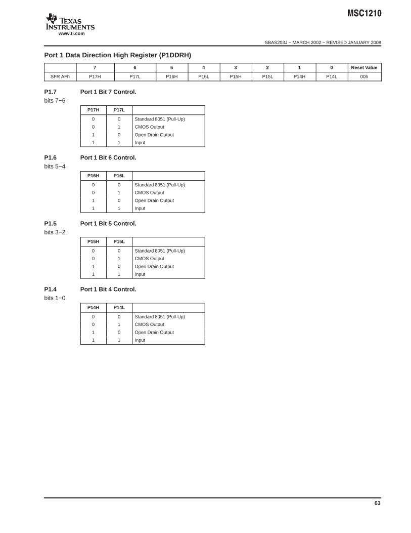
"#$%$&
SBAS203J − MARCH 2002 − REVISED JANUARY 2008
www.ti.com
63
Port 1 Data Direction High Register (P1DDRH)
7 6 5 4 3 2 1 0 Reset Value
SFR AFh P17H P17L P16H P16L P15H P15L P14H P14L 00h
P1.7 Port 1 Bit 7 Control.bits 7−6
P17H P17L
0 0 Standard 8051 (Pull-Up)
0 1 CMOS Output
1 0 Open Drain Output
1 1 Input
P1.6 Port 1 Bit 6 Control.bits 5−4
P16H P16L
0 0 Standard 8051 (Pull-Up)
0 1 CMOS Output
1 0 Open Drain Output
1 1 Input
P1.5 Port 1 Bit 5 Control.bits 3−2
P15H P15L
0 0 Standard 8051 (Pull-Up)
0 1 CMOS Output
1 0 Open Drain Output
1 1 Input
P1.4 Port 1 Bit 4 Control.bits 1−0
P14H P14L
0 0 Standard 8051 (Pull-Up)
0 1 CMOS Output
1 0 Open Drain Output
1 1 Input
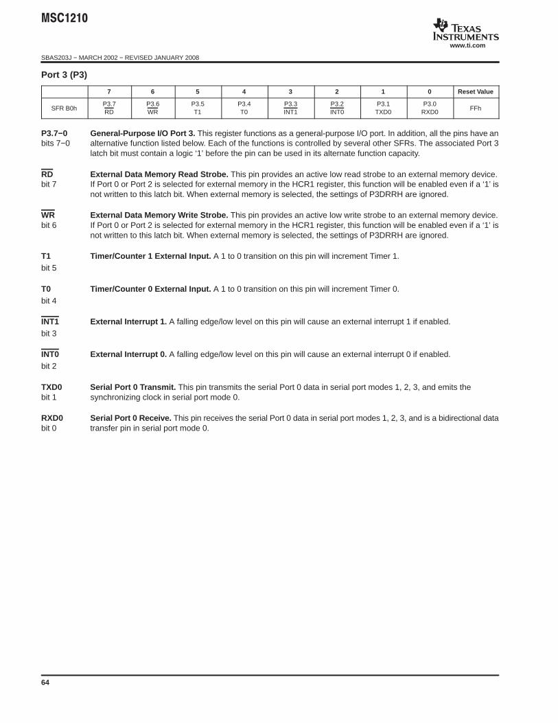
"#$%$&
SBAS203J − MARCH 2002 − REVISED JANUARY 2008
www.ti.com
64
Port 3 (P3)
7 6 5 4 3 2 1 0 Reset Value
SFR B0hP3.7RD
P3.6WR
P3.5T1
P3.4T0
P3.3INT1
P3.2INT0
P3.1TXD0
P3.0RXD0
FFh
P3.7−0 General-Purpose I/O Port 3. This register functions as a general-purpose I/O port. In addition, all the pins have anbits 7−0 alternative function listed below. Each of the functions is controlled by several other SFRs. The associated Port 3
latch bit must contain a logic ‘1’ before the pin can be used in its alternate function capacity.
RD External Data Memory Read Strobe. This pin provides an active low read strobe to an external memory device.bit 7 If Port 0 or Port 2 is selected for external memory in the HCR1 register, this function will be enabled even if a ‘1’ is
not written to this latch bit. When external memory is selected, the settings of P3DRRH are ignored.
WR External Data Memory Write Strobe. This pin provides an active low write strobe to an external memory device.bit 6 If Port 0 or Port 2 is selected for external memory in the HCR1 register, this function will be enabled even if a ‘1’ is
not written to this latch bit. When external memory is selected, the settings of P3DRRH are ignored.
T1 Timer/Counter 1 External Input. A 1 to 0 transition on this pin will increment Timer 1.bit 5
T0 Timer/Counter 0 External Input. A 1 to 0 transition on this pin will increment Timer 0.bit 4
INT1 External Interrupt 1. A falling edge/low level on this pin will cause an external interrupt 1 if enabled.bit 3
INT0 External Interrupt 0. A falling edge/low level on this pin will cause an external interrupt 0 if enabled.bit 2
TXD0 Serial Port 0 Transmit. This pin transmits the serial Port 0 data in serial port modes 1, 2, 3, and emits thebit 1 synchronizing clock in serial port mode 0.
RXD0 Serial Port 0 Receive. This pin receives the serial Port 0 data in serial port modes 1, 2, 3, and is a bidirectional databit 0 transfer pin in serial port mode 0.

"#$%$&
SBAS203J − MARCH 2002 − REVISED JANUARY 2008
www.ti.com
65
Port 2 Data Direction Low Register (P2DDRL)
7 6 5 4 3 2 1 0 Reset Value
SFR B1h P23H P23L P22H P22L P21H P21L P20H P20L 00h
P2.3 Port 2 Bit 3 Control.bits 7−6
P23H P23L
0 0 Standard 8051 (Pull-Up)
0 1 CMOS Output
1 0 Open Drain Output
1 1 Input
P2.2 Port 2 Bit 2 Control.bits 5−4
P22H P22L
0 0 Standard 8051 (Pull-Up)
0 1 CMOS Output
1 0 Open Drain Output
1 1 Input
P2.1 Port 2 Bit 1 Control.bits 3−2
P21H P21L
0 0 Standard 8051 (Pull-Up)
0 1 CMOS Output
1 0 Open Drain Output
1 1 Input
P2.0 Port 2 Bit 0 Control.bits 1−0
P20H P20L
0 0 Standard 8051 (Pull-Up)
0 1 CMOS Output
1 0 Open Drain Output
1 1 Input
NOTE: Port 2 also controlled by EA and Memory Access Control HCR1.1.
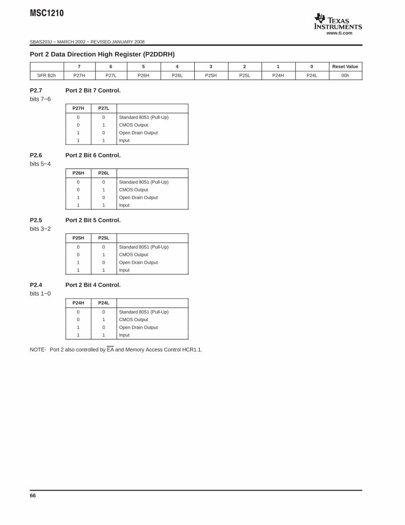
"#$%$&
SBAS203J − MARCH 2002 − REVISED JANUARY 2008
www.ti.com
66
Port 2 Data Direction High Register (P2DDRH)
7 6 5 4 3 2 1 0 Reset Value
SFR B2h P27H P27L P26H P26L P25H P25L P24H P24L 00h
P2.7 Port 2 Bit 7 Control.bits 7−6
P27H P27L
0 0 Standard 8051 (Pull-Up)
0 1 CMOS Output
1 0 Open Drain Output
1 1 Input
P2.6 Port 2 Bit 6 Control.bits 5−4
P26H P26L
0 0 Standard 8051 (Pull-Up)
0 1 CMOS Output
1 0 Open Drain Output
1 1 Input
P2.5 Port 2 Bit 5 Control.bits 3−2
P25H P25L
0 0 Standard 8051 (Pull-Up)
0 1 CMOS Output
1 0 Open Drain Output
1 1 Input
P2.4 Port 2 Bit 4 Control.bits 1−0
P24H P24L
0 0 Standard 8051 (Pull-Up)
0 1 CMOS Output
1 0 Open Drain Output
1 1 Input
NOTE: Port 2 also controlled by EA and Memory Access Control HCR1.1.

"#$%$&
SBAS203J − MARCH 2002 − REVISED JANUARY 2008
www.ti.com
67
Port 3 Data Direction Low Register (P3DDRL)
7 6 5 4 3 2 1 0 Reset Value
SFR B3h P33H P33L P32H P32L P31H P31L P30H P30L 00h
P3.3 Port 3 Bit 3 Control.bits 7−6
P33H P33L
0 0 Standard 8051 (Pull-Up)
0 1 CMOS Output
1 0 Open Drain Output
1 1 Input
P3.2 Port 3 Bit 2 Control.bits 5−4
P32H P32L
0 0 Standard 8051 (Pull-Up)
0 1 CMOS Output
1 0 Open Drain Output
1 1 Input
P3.1 Port 3 Bit 1 Control.bits 3−2
P31H P31L
0 0 Standard 8051 (Pull-Up)
0 1 CMOS Output
1 0 Open Drain Output
1 1 Input
P3.0 Port 3 Bit 0 Control.bits 1−0
P30H P30L
0 0 Standard 8051 (Pull-Up)
0 1 CMOS Output
1 0 Open Drain Output
1 1 Input

"#$%$&
SBAS203J − MARCH 2002 − REVISED JANUARY 2008
www.ti.com
68
Port 3 Data Direction High Register (P3DDRH)
7 6 5 4 3 2 1 0 Reset Value
SFR B4h P37H P37L P36H P36L P35H P35L P34H P34L 00h
P3.7 Port 3 Bit 7 Control.bits 7−6
P37H P37L
0 0 Standard 8051 (Pull-Up)
0 1 CMOS Output
1 0 Open Drain Output
1 1 Input
NOTE: Port 3.7 also controlled by EA and Memory Access Control HCR1.1.
P3.6 Port 3 Bit 6 Control.bits 5−4
P36H P36L
0 0 Standard 8051 (Pull-Up)
0 1 CMOS Output
1 0 Open Drain Output
1 1 Input
NOTE: Port 3.6 also controlled by EA and Memory Access Control HCR1.1.
P3.5 Port 3 Bit 5 Control.bits 3−2
P35H P35L
0 0 Standard 8051 (Pull-Up)
0 1 CMOS Output
1 0 Open Drain Output
1 1 Input
P3.4 Port 3 Bit 4 Control.bits 1−0
P34H P34L
0 0 Standard 8051 (Pull-Up)
0 1 CMOS Output
1 0 Open Drain Output
1 1 Input
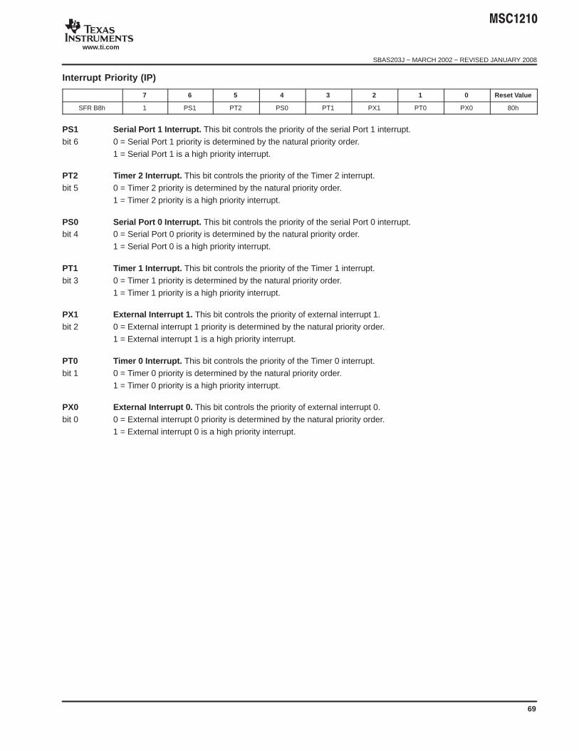
"#$%$&
SBAS203J − MARCH 2002 − REVISED JANUARY 2008
www.ti.com
69
Interrupt Priority (IP)
7 6 5 4 3 2 1 0 Reset Value
SFR B8h 1 PS1 PT2 PS0 PT1 PX1 PT0 PX0 80h
PS1 Serial Port 1 Interrupt. This bit controls the priority of the serial Port 1 interrupt.bit 6 0 = Serial Port 1 priority is determined by the natural priority order.
1 = Serial Port 1 is a high priority interrupt.
PT2 Timer 2 Interrupt. This bit controls the priority of the Timer 2 interrupt.bit 5 0 = Timer 2 priority is determined by the natural priority order.
1 = Timer 2 priority is a high priority interrupt.
PS0 Serial Port 0 Interrupt. This bit controls the priority of the serial Port 0 interrupt.bit 4 0 = Serial Port 0 priority is determined by the natural priority order.
1 = Serial Port 0 is a high priority interrupt.
PT1 Timer 1 Interrupt. This bit controls the priority of the Timer 1 interrupt.bit 3 0 = Timer 1 priority is determined by the natural priority order.
1 = Timer 1 priority is a high priority interrupt.
PX1 External Interrupt 1. This bit controls the priority of external interrupt 1.bit 2 0 = External interrupt 1 priority is determined by the natural priority order.
1 = External interrupt 1 is a high priority interrupt.
PT0 Timer 0 Interrupt. This bit controls the priority of the Timer 0 interrupt.bit 1 0 = Timer 0 priority is determined by the natural priority order.
1 = Timer 0 priority is a high priority interrupt.
PX0 External Interrupt 0. This bit controls the priority of external interrupt 0.bit 0 0 = External interrupt 0 priority is determined by the natural priority order.
1 = External interrupt 0 is a high priority interrupt.
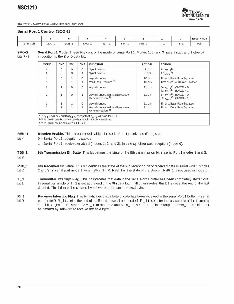
"#$%$&
SBAS203J − MARCH 2002 − REVISED JANUARY 2008
www.ti.com
70
Serial Port 1 Control (SCON1)
7 6 5 4 3 2 1 0 Reset Value
SFR C0h SM0_1 SM1_1 SM2_1 REN_1 TB8_1 RB8_1 TI_1 RI_1 00h
SM0−2 Serial Port 1 Mode. These bits control the mode of serial Port 1. Modes 1, 2, and 3 have 1 start and 1 stop bitbits 7−5 in addition to the 8 or 9 data bits.
MODE SM0 SM1 SM2 FUNCTION LENGTH PERIOD
0 0 0 0 Synchronous 8 bits 12 pCLK(1)
0 0 0 1 Synchronous 8 bits 4 pCLK(1)
1 0 1 0 Asynchronous 10 bits Timer 1 Baud Rate Equation1 0 1 1 Valid Stop Required(2) 10 bits Timer 1 or Baud Rate Equation
2 1 0 0 Asynchronous 11 bits 64 pCLK(1) (SMOD = 0)32 pCLK(1) (SMOD = 1)
2 1 0 1 Asynchronous with MultiprocessorCommunication(3)
11 bits 64 pCLK(1) (SMOD = 0)32 pCLK(1) (SMOD = 1)
3 1 1 0 Asynchronous 11 bits Timer 1 Baud Rate Equation3 1 1 1 Asynchronous with Multiprocessor
Communication(3)11 bits Timer 1 Baud Rate Equation
(1) pCLK will be equal to tCLK, except that pCLK will stop for IDLE.(2) RI_0 will only be activated when a valid STOP is received.(3) RI_0 will not be activated if bit 9 = 0.
REN_1 Receive Enable. This bit enables/disables the serial Port 1 received shift register.bit 4 0 = Serial Port 1 reception disabled.
1 = Serial Port 1 received enabled (modes 1, 2, and 3). Initiate synchronous reception (mode 0).
TB8_1 9th Transmission Bit State. This bit defines the state of the 9th transmission bit in serial Port 1 modes 2 and 3.bit 3
RB8_1 9th Received Bit State. This bit identifies the state of the 9th reception bit of received data in serial Port 1 modesbit 2 2 and 3. In serial port mode 1, when SM2_1 = 0, RB8_1 is the state of the stop bit. RB8_1 is not used in mode 0.
TI_1 Transmitter Interrupt Flag. This bit indicates that data in the serial Port 1 buffer has been completely shifted out.bit 1 In serial port mode 0, TI_1 is set at the end of the 8th data bit. In all other modes, this bit is set at the end of the last
data bit. This bit must be cleared by software to transmit the next byte.
RI_1 Receiver Interrupt Flag. This bit indicates that a byte of data has been received in the serial Port 1 buffer. In serialbit 0 port mode 0, RI_1 is set at the end of the 8th bit. In serial port mode 1, RI_1 is set after the last sample of the incoming
stop bit subject to the state of SM2_1. In modes 2 and 3, RI_1 is set after the last sample of RB8_1. This bit mustbe cleared by software to receive the next byte.

"#$%$&
SBAS203J − MARCH 2002 − REVISED JANUARY 2008
www.ti.com
71
Serial Data Buffer 1 (SBUF1)
7 6 5 4 3 2 1 0 Reset Value
SFR C1h 00h
SBUF1.7−0 Serial Data Buffer 1. Data for serial Port 1 is read from or written to this location. The serial transmit and receivebits 7−0 buffers are separate registers, but both are addressed at this location.
Enable Wake Up (EWU) Waking Up from IDLE Mode
7 6 5 4 3 2 1 0 Reset Value
SFR C6h — — — — — EWUWDT EWUEX1 EWUEX0 00h
Auxiliary interrupts will wake up from IDLE. They are enabled with EAI (EICON.5, SFR D8h).
EWUWDT Enable Wake Up Watchdog Timer. Wake using watchdog timer interrupt.bit 2 0 = Don’t wake up on watchdog timer interrupt.
1 = Wake up on watchdog timer interrupt.
EWUEX1 Enable Wake Up External 1. Wake using external interrupt source 1.bit 1 0 = Don’t wake up on external interrupt source 1.
1 = Wake up on external interrupt source 1.
EWUEX0 Enable Wake Up External 0. Wake using external interrupt source 0.bit 0 0 = Don’t wake up on external interrupt source 0.
1 = Wake up on external interrupt source 0.

"#$%$&
SBAS203J − MARCH 2002 − REVISED JANUARY 2008
www.ti.com
72
Timer 2 Control (T2CON)
7 6 5 4 3 2 1 0 Reset Value
SFR C8h TF2 EXF2 RCLK TCLK EXEN2 TR2 C/T2 CP/RL2 00h
TF2 Timer 2 Overflow Flag. This flag will be set when Timer 2 overflows from FFFFh. It must be cleared by software.bit 7 TF2 will only be set if RCLK and TCLK are both cleared to 0. Writing a 1 to TF2 forces a Timer 2 interrupt if enabled.
EXF2 Timer 2 External Flag. A negative transition on the T2EX pin (P1.1) will cause this flag to be set based on the EXEN2bit 6 (T2CON.3) bit. If set by a negative transition, this flag must be cleared to 0 by software. Setting this bit in software
will force a timer interrupt if enabled.
RCLK Receive Clock Flag. This bit determines the serial Port 0 timebase when receiving data in serial modes 1 or 3.bit 5 0 = Timer 1 overflow is used to determine receiver baud rate for USART0.
1 = Timer 2 overflow is used to determine receiver baud rate for USART0.Setting this bit will force Timer 2 into baud rate generation mode. The timer will operate from a divide by 2 of theexternal clock.
TCLK Transmit Clock Flag. This bit determines the serial Port 0 timebase when transmitting data in serial modes 1 or 3.bit 4 0 = Timer 1 overflow is used to determine transmitter baud rate for USART0.
1 = Timer 2 overflow is used to determine transmitter baud rate for USART0.Setting this bit will force Timer 2 into baud rate generation mode. The timer will operate from a divide by 2 of theexternal clock.
EXEN2 Timer 2 External Enable. This bit enables the capture/reload function on the T2EX pin if Timer 2 is not generatingbit 3 baud rates for the serial port.
0 = Timer 2 will ignore all external events at T2EX.1 = Timer 2 will capture or reload a value if a negative transition is detected on the T2EX pin.
TR2 Timer 2 Run Control. This bit enables/disables the operation of Timer 2. Halting this timer will preserve the currentbit 2 count in TH2, TL2.
0 = Timer 2 is halted.1 = Timer 2 is enabled.
C/T2 Counter/Timer Select. This bit determines whether Timer 2 will function as a timer or counter. Independent of thisbit 1 bit, Timer 2 runs at 2 clocks per tick when used in baud rate generator mode.
0 = Timer 2 functions as a timer. The speed of Timer 2 is determined by the T2M bit (CKCON.5).1 = Timer 2 will count negative transitions on the T2 pin (P1.0).
CP/RL2 Capture/Reload Select. This bit determines whether the capture or reload function is used for Timer 2. If either RCLKbit 0 or TCLK is set, this bit will not function and the timer will function in an auto-reload mode following each overflow.
0 = Auto-reloads will occur when Timer 2 overflows or a falling edge is detected on T2EX if EXEN2 = 1.1 = Timer 2 captures will occur when a falling edge is detected on T2EX if EXEN2 = 1.
Timer 2 Capture LSB (RCAP2L)
7 6 5 4 3 2 1 0 Reset Value
SFR CAh 00h
RCAP2L Timer 2 Capture LSB. This register is used to capture the TL2 value when Timer 2 is configured in capture mode.bits 7−0 RCAP2L is also used as the LSB of a 16-bit reload value when Timer 2 is configured in auto-reload mode.
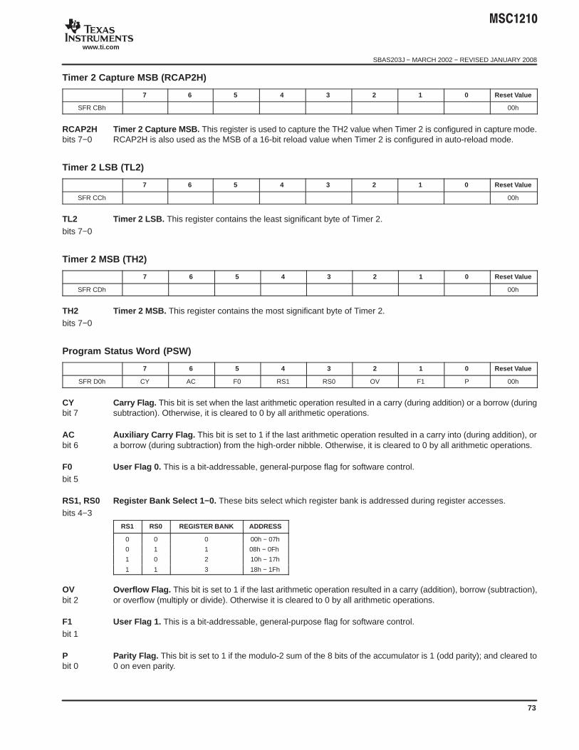
"#$%$&
SBAS203J − MARCH 2002 − REVISED JANUARY 2008
www.ti.com
73
Timer 2 Capture MSB (RCAP2H)
7 6 5 4 3 2 1 0 Reset Value
SFR CBh 00h
RCAP2H Timer 2 Capture MSB. This register is used to capture the TH2 value when Timer 2 is configured in capture mode.bits 7−0 RCAP2H is also used as the MSB of a 16-bit reload value when Timer 2 is configured in auto-reload mode.
Timer 2 LSB (TL2)
7 6 5 4 3 2 1 0 Reset Value
SFR CCh 00h
TL2 Timer 2 LSB. This register contains the least significant byte of Timer 2.bits 7−0
Timer 2 MSB (TH2)
7 6 5 4 3 2 1 0 Reset Value
SFR CDh 00h
TH2 Timer 2 MSB. This register contains the most significant byte of Timer 2.bits 7−0
Program Status Word (PSW)
7 6 5 4 3 2 1 0 Reset Value
SFR D0h CY AC F0 RS1 RS0 OV F1 P 00h
CY Carry Flag. This bit is set when the last arithmetic operation resulted in a carry (during addition) or a borrow (duringbit 7 subtraction). Otherwise, it is cleared to 0 by all arithmetic operations.
AC Auxiliary Carry Flag. This bit is set to 1 if the last arithmetic operation resulted in a carry into (during addition), orbit 6 a borrow (during subtraction) from the high-order nibble. Otherwise, it is cleared to 0 by all arithmetic operations.
F0 User Flag 0. This is a bit-addressable, general-purpose flag for software control.bit 5
RS1, RS0 Register Bank Select 1−0. These bits select which register bank is addressed during register accesses.bits 4−3
RS1 RS0 REGISTER BANK ADDRESS
0 0 0 00h − 07h
0 1 1 08h − 0Fh
1 0 2 10h − 17h
1 1 3 18h − 1Fh
OV Overflow Flag. This bit is set to 1 if the last arithmetic operation resulted in a carry (addition), borrow (subtraction),bit 2 or overflow (multiply or divide). Otherwise it is cleared to 0 by all arithmetic operations.
F1 User Flag 1. This is a bit-addressable, general-purpose flag for software control.bit 1
P Parity Flag. This bit is set to 1 if the modulo-2 sum of the 8 bits of the accumulator is 1 (odd parity); and cleared tobit 0 0 on even parity.
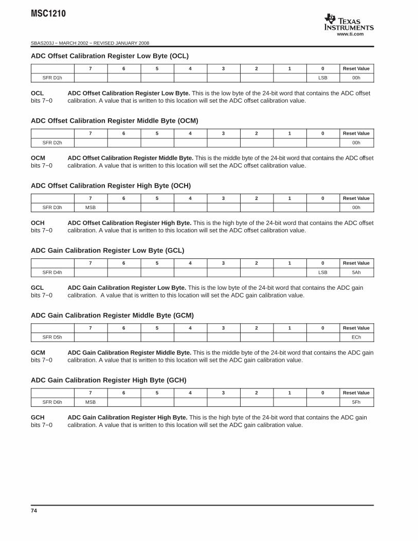
"#$%$&
SBAS203J − MARCH 2002 − REVISED JANUARY 2008
www.ti.com
74
ADC Offset Calibration Register Low Byte (OCL)
7 6 5 4 3 2 1 0 Reset Value
SFR D1h LSB 00h
OCL ADC Offset Calibration Register Low Byte. This is the low byte of the 24-bit word that contains the ADC offsetbits 7−0 calibration. A value that is written to this location will set the ADC offset calibration value.
ADC Offset Calibration Register Middle Byte (OCM)
7 6 5 4 3 2 1 0 Reset Value
SFR D2h 00h
OCM ADC Offset Calibration Register Middle Byte. This is the middle byte of the 24-bit word that contains the ADC offsetbits 7−0 calibration. A value that is written to this location will set the ADC offset calibration value.
ADC Offset Calibration Register High Byte (OCH)
7 6 5 4 3 2 1 0 Reset Value
SFR D3h MSB 00h
OCH ADC Offset Calibration Register High Byte. This is the high byte of the 24-bit word that contains the ADC offsetbits 7−0 calibration. A value that is written to this location will set the ADC offset calibration value.
ADC Gain Calibration Register Low Byte (GCL)
7 6 5 4 3 2 1 0 Reset Value
SFR D4h LSB 5Ah
GCL ADC Gain Calibration Register Low Byte. This is the low byte of the 24-bit word that contains the ADC gainbits 7−0 calibration. A value that is written to this location will set the ADC gain calibration value.
ADC Gain Calibration Register Middle Byte (GCM)
7 6 5 4 3 2 1 0 Reset Value
SFR D5h ECh
GCM ADC Gain Calibration Register Middle Byte. This is the middle byte of the 24-bit word that contains the ADC gainbits 7−0 calibration. A value that is written to this location will set the ADC gain calibration value.
ADC Gain Calibration Register High Byte (GCH)
7 6 5 4 3 2 1 0 Reset Value
SFR D6h MSB 5Fh
GCH ADC Gain Calibration Register High Byte. This is the high byte of the 24-bit word that contains the ADC gainbits 7−0 calibration. A value that is written to this location will set the ADC gain calibration value.
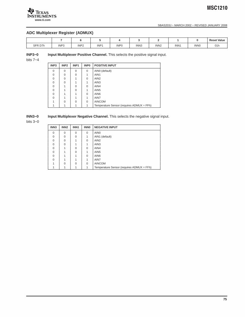
"#$%$&
SBAS203J − MARCH 2002 − REVISED JANUARY 2008
www.ti.com
75
ADC Multiplexer Register (ADMUX)
7 6 5 4 3 2 1 0 Reset Value
SFR D7h INP3 INP2 INP1 INP0 INN3 INN2 INN1 INN0 01h
INP3−0 Input Multiplexer Positive Channel. This selects the positive signal input.bits 7−4
INP3 INP2 INP1 INP0 POSITIVE INPUT
0 0 0 0 AIN0 (default)0 0 0 1 AIN10 0 1 0 AIN20 0 1 1 AIN30 1 0 0 AIN40 1 0 1 AIN50 1 1 0 AIN60 1 1 1 AIN71 0 0 0 AINCOM1 1 1 1 Temperature Sensor (requires ADMUX = FFh)
INN3−0 Input Multiplexer Negative Channel. This selects the negative signal input.bits 3−0
INN3 INN2 INN1 INN0 NEGATIVE INPUT
0 0 0 0 AIN00 0 0 1 AIN1 (default)0 0 1 0 AIN20 0 1 1 AIN30 1 0 0 AIN40 1 0 1 AIN50 1 1 0 AIN60 1 1 1 AIN71 0 0 0 AINCOM1 1 1 1 Temperature Sensor (requires ADMUX = FFh)

"#$%$&
SBAS203J − MARCH 2002 − REVISED JANUARY 2008
www.ti.com
76
Enable Interrupt Control (EICON)
7 6 5 4 3 2 1 0 Reset Value
SFR D8h SMOD1 1 EAI AI WDTI 0 0 0 40h
SMOD1 Serial Port 1 Mode. When this bit is set the serial baud rate for Port 1 will be doubled.bit 7 0 = Standard baud rate for Port 1 (default).
1 = Double baud rate for Port 1.
EAI Enable Auxiliary Interrupt. The Auxiliary Interrupt accesses nine different interrupts which are masked andbit 5 identified by SFR registers PAI (SFR A5h), AIE (SFR A6h), and AISTAT (SFR A7h).
0 = Auxiliary Interrupt disabled (default).1 = Auxiliary Interrupt enabled.
AI Auxiliary Interrupt Flag. AI must be cleared by software before exiting the interrupt service routine, after the sourcebit 4 of the interrupt is cleared. Otherwise, the interrupt occurs again. Setting AI in software generates an Auxiliary
Interrupt, if enabled.0 = No Auxiliary Interrupt detected (default).1 = Auxiliary Interrupt detected.
WDTI Watchdog T imer Interrupt Flag. WDTI must be cleared by software before exiting the interrupt service routine. bit 3 Otherwise, the interrupt will occur again. Setting WDTI in software generates a watchdog time interrupt, if enabled.
The Watchdog timer can generate an interrupt or reset. The interrupt is available only if the reset action is disabledin HCR0.0 = No Watchdog Timer Interrupt detected (default).1 = Watchdog Timer Interrupt detected.
ADC Results Register Low Byte (ADRESL)
7 6 5 4 3 2 1 0 Reset Value
SFR D9h LSB 00h
ADRESL The ADC Results Low Byte. This is the low byte of the 24-bit word that contains the ADC converter results.bits 7−0 Reading from this register clears the ADC interrupt. However, AI in EICON (SFR D8h) must also be cleared.
ADC Results Register Middle Byte (ADRESM)
7 6 5 4 3 2 1 0 Reset Value
SFR DAh 00h
ADRESM The ADC Results Middle Byte. This is the middle byte of the 24-bit word that contains the ADC converter results.bits 7−0
ADC Results Register High Byte (ADRESH)
7 6 5 4 3 2 1 0 Reset Value
SFR DBh MSB 00h
ADRESH The ADC Results High Byte. This is the high byte of the 24-bit word that contains the ADC converter results.bits 7−0
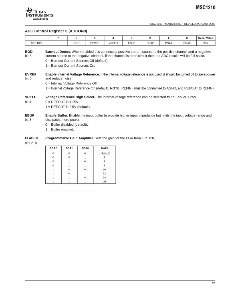
"#$%$&
SBAS203J − MARCH 2002 − REVISED JANUARY 2008
www.ti.com
77
ADC Control Register 0 (ADCON0)
7 6 5 4 3 2 1 0 Reset Value
SFR DCh BOD EVREF VREFH EBUF PGA2 PGA1 PGA0 30h
BOD Burnout Detect. When enabled this connects a positive current source to the positive channel and a negativebit 6 current source to the negative channel. If the channel is open circuit then the ADC results will be full-scale.
0 = Burnout Current Sources Off (default).1 = Burnout Current Sources On.
EVREF Enable Internal V oltage Reference. If the internal voltage reference is not used, it should be turned off to save powerbit 5 and reduce noise.
0 = Internal Voltage Reference Off.1 = Internal Voltage Reference On (default). NOTE: REFIN− must be connected to AGND, and REFOUT to REFIN+.
VREFH Voltage Reference High Select. The internal voltage reference can be selected to be 2.5V or 1.25V.bit 4 0 = REFOUT is 1.25V.
1 = REFOUT is 2.5V (default).
EBUF Enable Buffer. Enable the input buffer to provide higher input impedance but limits the input voltage range andbit 3 dissipates more power.
0 = Buffer disabled (default).1 = Buffer enabled.
PGA2−0 Programmable Gain Amplifier. Sets the gain for the PGA from 1 to 128.bits 2−0
PGA2 PGA1 PGA0 GAIN
0 0 0 1 (default)
0 0 1 2
0 1 0 4
0 1 1 8
1 0 0 16
1 0 1 32
1 1 0 64
1 1 1 128

"#$%$&
SBAS203J − MARCH 2002 − REVISED JANUARY 2008
www.ti.com
78
ADC Control Register 1 (ADCON1)
7 6 5 4 3 2 1 0 Reset Value
SFR DDh — POL SM1 SM0 — CAL2 CAL1 CAL0 0000 0000b
POL Polarity. Polarity of the ADC result and Summation register.bit 6 0 = Bipolar.
1 = Unipolar. The LSB size is 1/2 the size of bipolar (twice the resolution).
POL ANALOG INPUT DIGITAL OUTPUT
+FSR 7FFFFFh
0 ZERO 000000h0−FSR 800000h
+FSR FFFFFFh
1 ZERO 000000h1
−FSR 000000h
SM1−0 Settling Mode. Selects the type of filter or auto select which defines the digital filter settling characteristics.bits 5−4
SM1 SM0 SETTLING MODE
0 0 Auto
0 1 Fast Settling Filter
1 0 Sinc2 Filter
1 1 Sinc3 Filter
CAL2−0 Calibration Mode Control Bits.bits 2−0 Writing to these bits starts ADC calibration.
CAL2 CAL1 CAL0 CALIBRATION MODE
0 0 0 No Calibration (default)
0 0 1 Self-Calibration, Offset and Gain
0 1 0 Self-Calibration, Offset only
0 1 1 Self-Calibration, Gain only
1 0 0 System Calibration, Offset only (requires external connection)
1 0 1 System Calibration, Gain only (requires external connection)
1 1 0 Reserved
1 1 1 Reserved
NOTE: Read Value—000b.
ADC Control Register 2 (ADCON2)
7 6 5 4 3 2 1 0 Reset Value
SFR DEh DR7 DR6 DR5 DR4 DR3 DR2 DR1 DR0 1Bh
DR7−0 Decimation Ratio LSB.bits 7−0
ADC Control Register 3 (ADCON3)
7 6 5 4 3 2 1 0 Reset Value
SFR DFh — — — — — DR10 DR9 DR8 06h
DR10−8 Decimation Ratio Most Significant 3 Bits. The output data rate = fCLK/[(ACLK + 1) 64 Decimation Ratio].bits 2−0

"#$%$&
SBAS203J − MARCH 2002 − REVISED JANUARY 2008
www.ti.com
79
Accumulator (A or ACC)
7 6 5 4 3 2 1 0 Reset Value
SFR E0h ACC.7 ACC.6 ACC.5 ACC.4 ACC.3 ACC.2 ACC.1 ACC.0 00h
ACC.7−0 Accumulator. This register serves as the accumulator for arithmetic and logic operations.bits 7−0
Summation/Shifter Control (SSCON)
7 6 5 4 3 2 1 0 Reset Value
SFR E1h SSCON1 SSCON0 SCNT2 SCNT1 SCNT0 SHF2 SHF1 SHF0 00h
The Summation register is powered down when the ADC is powered down. If all zeroes are written to this register the 32-bitSUMR3−0 registers will be cleared. The Summation registers will do sign extend if Bipolar is selected in ADCON1.
SSCON1−0 Summation/Shift Count.bits 7−6
SOURCE SSCON1 SSCON0 MODE
CPU 0 0 Values written to the SUM registers are accumulated when the SUMR0 value is written (sum/shift ignored)
ADC 0 1 Summation register Enabled. Source is ADC, summation count is working.
CPU 1 0 Shift Enabled. Summation register is shifted by SHF Count bits. It takes four system clocks to execute.
ADC 1 1 Accumulate and Shift Enable. Values are accumulated for SUM Count times and then shifted by SHF Count.
SCNT2−0 Summation Count. When the summation is complete an interrupt will be generated unless masked. Reading thebits 5−3 SUMR0 register clears the interrupt.
SCNT2 SCNT1 SCNT0 SUMMATION COUNT
0 0 0 2
0 0 1 4
0 1 0 8
0 1 1 16
1 0 0 32
1 0 1 64
1 1 0 128
1 1 1 256
SHF2−0 Shift Count.bits 2−0
SHF2 SHF1 SHF0 SHIFT DIVIDE
0 0 0 1 2
0 0 1 2 4
0 1 0 3 8
0 1 1 4 16
1 0 0 5 32
1 0 1 6 64
1 1 0 7 128
1 1 1 8 256

"#$%$&
SBAS203J − MARCH 2002 − REVISED JANUARY 2008
www.ti.com
80
Summation Register 0 (SUMR0)
7 6 5 4 3 2 1 0 Reset Value
SFR E2h LSB 00h
SUMR0 Summation Register 0. This is the least significant byte of the 32-bit summation register or bits 0 to 7.bits 7−0 Write: Will cause values in SUMR3−0 to be added to the summation register.
Read: Will clear the Summation Count Interrupt. AI in EICON (SFR D8h) must also be cleared.
Summation Register 1 (SUMR1)
7 6 5 4 3 2 1 0 Reset Value
SFR E3h 00h
SUMR1 Summation Register 1. These are bits 8−15 of the 32-bit summation register.bits 7−0
Summation Register 2 (SUMR2)
7 6 5 4 3 2 1 0 Reset Value
SFR E4h 00h
SUMR2 Summation Register 2. These are bits 16−23 of the 32-bit summation register.bits 7−0
Summation Register 3 (SUMR3)
7 6 5 4 3 2 1 0 Reset Value
SFR E5h MSB 00h
SUMR3 Summation Register 3. This is the most significant byte of the 32-bit summation register or bits 24−31.bits 7−0
Offset DAC Register (ODAC)
7 6 5 4 3 2 1 0 Reset Value
SFR E6h 00h
ODAC Offset DAC Register. This register will shift the input by up to half of the ADC full-scale input range. The offset DACbits 7−0 value is summed with the ADC input prior to conversion. Writing 00h or 80h to ODAC turns off the offset DAC.bit 7 Offset DAC Sign bit.
0 = Positive1 = Negative
bit 6−0 Offset VREF
2 PGA ODAC 6 : 0
127 ( 1)bit7
NOTE: ODAC cannot be used to offset the input so that the buffer can be used for AGND signals. Offset DAC should becleared before offset calibration, since the offset DAC output is applied directly to the ADC input.

"#$%$&
SBAS203J − MARCH 2002 − REVISED JANUARY 2008
www.ti.com
81
Low Voltage Detect Control (LVDCON)
7 6 5 4 3 2 1 0 Reset Value
SFR E7h ALVDIS ALVD2 ALVD1 ALVD0 DLVDIS DLVD2 DLVD1 DLVD0 00h
NOTE: By default, both analog and digital low-voltage detections are enabled, which causes approximately 25µA ofcurrent consumption from the power supply. To minimize this power consumption, both low-voltage detections should bedisabled before entering Stop mode.
ALVDIS Analog Low Voltage Detect Disable.bit 7 0 = Enable Detection of Low Analog Supply Voltage
1 = Disable Detection of Low Analog Supply Voltage
ALVD2−0 Analog Voltage Detection Level.bits 6−4
ALVD2 ALVD1 ALVD0 VOLTAGE LEVEL
0 0 0 AVDD 2.7V (default)
0 0 1 AVDD 3.0V
0 1 0 AVDD 3.3V
0 1 1 AVDD 4.0V
1 0 0 AVDD 4.2V
1 0 1 AVDD 4.5V
1 1 0 AVDD 4.7V
1 1 1 External Voltage AIN7 compared to1.2V
DLVDIS Digital Low Voltage Detect Disable.bit 3 0 = Enable Detection of Low Digital Supply Voltage
1 = Disable Detection of Low Digital Supply Voltage
DLVD2−0 Digital Voltage Detection Level.bits 2−0
DLVD2 DLVD1 DLVD0 VOLTAGE LEVEL
0 0 0 DVDD 2.7V (default)
0 0 1 DVDD 3.0V
0 1 0 DVDD 3.3V
0 1 1 DVDD 4.0V
1 0 0 DVDD 4.2V
1 0 1 DVDD 4.5V
1 1 0 DVDD 4.7V
1 1 1 External Voltage AIN6 compared to1.2V

"#$%$&
SBAS203J − MARCH 2002 − REVISED JANUARY 2008
www.ti.com
82
Extended Interrupt Enable (EIE)
7 6 5 4 3 2 1 0 Reset Value
SFR E8h 1 1 1 EWDI EX5 EX4 EX3 EX2 E0h
EWDI Enable Watchdog Interrupt. This bit enables/disables the watchdog interrupt. The Watchdog timer is enabled bybit 4 (SFR FFh) and PDCON (SFR F1h) registers.
0 = Disable the Watchdog Interrupt1 = Enable Interrupt Request Generated by the Watchdog Timer
EX5 External Interrupt 5 Enable. This bit enables/disables external interrupt 5.bit 3 0 = Disable External Interrupt 5
1 = Enable External Interrupt 5
EX4 External Interrupt 4 Enable. This bit enables/disables external interrupt 4.bit 2 0 = Disable External Interrupt 4
1 = Enable External Interrupt 4
EX3 External Interrupt 3 Enable. This bit enables/disables external interrupt 3.bit 1 0 = Disable External Interrupt 3
1 = Enable External Interrupt 3
EX2 External Interrupt 2 Enable. This bit enables/disables external interrupt 2.bit 0 0 = Disable External Interrupt 2
1 = Enable External Interrupt 2
Hardware Product Code Register 0 (HWPC0) (read-only)
7 6 5 4 3 2 1 0 Reset Value
SFR E9h 0 0 0 0 0 0 MEMORY SIZE 0000_00xxb
HWPC1.7−0 Hardware Product Code LSB. Read-only.bits 7−0
MEMORYSIZE MODEL
FLASHMEMORY
0 0 MSC1210Y2 4kB
0 1 MSC1210Y3 8kB
1 0 MSC1210Y4 16kB
1 1 MSC1210Y5 32kB
Hardware Product Code Register 1 (HWPC1) (read-only)
7 6 5 4 3 2 1 0 Reset Value
SFR EAh 0 0 0 0 0 0 0 0 00h
HWPC1.7−0 Hardware Product Code MSB. Read-only.bits 7−0

"#$%$&
SBAS203J − MARCH 2002 − REVISED JANUARY 2008
www.ti.com
83
Hardware Version Register (HDWVER)
7 6 5 4 3 2 1 0 Reset Value
SFR EBh
Flash Memory Control (FMCON)
7 6 5 4 3 2 1 0 Reset Value
SFR EEh 0 PGERA 0 FRCM 0 BUSY 1 0 02h
PGERA Page Erase.bit 6 0 = MOVX to Flash will perform a byte write operation
1 = MOVX to Flash will perform a page erase operation
FRCM Frequency Control Mode.bit 4 0 = Bypass (default)
1 = Use Delay Line. Saves power when reading Flash (recommended)
BUSY Write/Erase BUSY Signal.bit 2 0 = Idle or Available
1 = Busy
Flash Memory Timing Control Register (FTCON)
7 6 5 4 3 2 1 0 Reset Value
SFR EFh FER3 FER2 FER1 FER0 FWR3 FWR2 FWR1 FWR0 A5h
Refer to Flash Timing Characteristics.
FER3−0 Set Erase. Flash Erase Time = (1 + FER) • (MSEC + 1) • tCLK.bits 7−4 A minimum of 10ms is needed for industrial temperature range.
A minimum of 4ms is needed for commercial temperature range.
FWR3−0 Set Write. Flash Write Time = (1 + FWR) • (USEC + 1) • 5 • tCLK.bits 3−0 Write time should be 30−40µs.
B Register (B)
7 6 5 4 3 2 1 0 Reset Value
SFR F0h B.7 B.6 B.5 B.4 B.3 B.2 B.1 B.0 00h
B.7−0 B Register. This register serves as a second accumulator for certain arithmetic operations.bits 7−0

"#$%$&
SBAS203J − MARCH 2002 − REVISED JANUARY 2008
www.ti.com
84
Power-Down Control Register (PDCON)
7 6 5 4 3 2 1 0 Reset Value
SFR F1h 0 0 0 PDPWM PDADC PDWDT PDST PDSPI 1Fh
Turning peripheral modules off puts the MSC1210 in the lowest power mode.
PDPWM Pulse Width Module Control.bit 4 0 = PWM On
1 = PWM Power Down
PDADC ADC Control.bit 3 0 = ADC On
1 = ADC, VREF, and summation registers are powered down.
PDWDT Watchdog Timer Control.bit 2 0 = Watchdog Timer On
1 = Watchdog Timer Power Down
PDST System Timer Control.bit 1 0 = System Timer On
1 = System Timer Power Down
PDSPI SPI System Control.bit 0 0 = SPI System On
1 = SPI System Power Down
PSEN/ALE Select (PASEL)
7 6 5 4 3 2 1 0 Reset Value
SFR F2h 0 0 PSEN2 PSEN1 PSEN0 0 ALE1 ALE0 00h
PSEN2−0 PSEN Mode Select.bits 5−3
PSEN2 PSEN1 PSEN0
0 0 x PSEN
0 1 x CLK
1 0 x ADCMODCLK
1 1 0 LOW
1 1 1 HIGH
ALE1−0 ALE Mode Select.bits 1−0
ALE1 ALE0
0 x ALE
1 0 LOW
1 1 HIGH
NOTE: For power-saving purposes, it is recommended that the PSEN and ALE pins be set to low or high mode whenexternal memory is not used.

"#$%$&
SBAS203J − MARCH 2002 − REVISED JANUARY 2008
www.ti.com
85
Analog Clock (ACLK)
7 6 5 4 3 2 1 0 Reset Value
SFR F6h 0 FREQ6 FREQ5 FREQ4 FREQ3 FREQ2 FREQ1 FREQ0 03h
FREQ6−0 Clock Frequency − 1. This value + 1 divides the system clock to create the ADC clock.
bit 6−0 fACLK fCLK
FREQ 1
fCLK
ACLK 1
fMOD fCLK
(ACLK 1) 64
Output Data Rate fMOD
Decimation
System Reset Register (SRST)
7 6 5 4 3 2 1 0 Reset Value
SFR F7h 0 0 0 0 0 0 0 RSTREQ 00h
RSTREQ Reset Request. Setting this bit to 1 and then clearing to 0 will generate a system reset.bit 0
Extended Interrupt Priority (EIP)
7 6 5 4 3 2 1 0 Reset Value
SFR F8h 1 1 1 PWDI PX5 PX4 PX3 PX2 E0h
PWDI Watchdog Interrupt Priority. This bit controls the priority of the watchdog interrupt.bit 4 0 = The watchdog interrupt is low priority.
1 = The watchdog interrupt is high priority.
PX5 External Interrupt 5 Priority. This bit controls the priority of external interrupt 5.bit 3 0 = External interrupt 5 is low priority.
1 = External interrupt 5 is high priority.
PX4 External Interrupt 4 Priority. This bit controls the priority of external interrupt 4.bit 2 0 = External interrupt 4 is low priority.
1 = External interrupt 4 is high priority.
PX3 External Interrupt 3 Priority. This bit controls the priority of external interrupt 3.bit 1 0 = External interrupt 3 is low priority.
1 = External interrupt 3 is high priority.
PX2 External Interrupt 2 Priority. This bit controls the priority of external interrupt 2.bit 0 0 = External interrupt 2 is low priority.
1 = External interrupt 2 is high priority.
"#$%$&
SBAS203J − MARCH 2002 − REVISED JANUARY 2008
www.ti.com
86
Seconds Timer Interrupt (SECINT)
7 6 5 4 3 2 1 0 Reset Value
SFR F9h WRT SECINT6 SECINT5 SECINT4 SECINT3 SECINT2 SECINT1 SECINT0 7Fh
This system clock is divided by the value of the 16-bit register MSECH:MSECL. Then, the 1ms timer tick is divided by theregister HMSEC that provides the 100ms signal used by this seconds timer. Therefore, the seconds timer can generatean interrupt that occurs from 100ms to 12.8 seconds. Reading this register clears the Seconds Interrupt. This Interrupt canbe monitored in the AIE register.
WRT Write Control. Determines whether to write the value immediately or wait until the current count is finished.bit 7 Read = 0.
0 = Delay Write Operation. The SEC value is loaded when the current count expires.1 = Write Immediately. The counter is loaded once the CPU completes the write operation.
SECINT6−0 Seconds Count. Normal operation uses 100ms as the clock interval, and would equal: (SEC + 1)/10 seconds.bits 6−0 Seconds Interrupt = (1 + SEC) • (HMSEC + 1) • (MSEC + 1) • tCLK
Milliseconds Interrupt (MSINT)
7 6 5 4 3 2 1 0 Reset Value
SFR FAh WRT MSINT6 MSINT5 MSINT4 MSINT3 MSINT2 MSINT1 MSINT0 7Fh
The clock used for this timer is the 1ms clock, which results from dividing the system clock by the values in registersMSECH:MSECL. Reading this register clears the milliseconds interrupt. AI in EICON (SFR D8h) must also be cleared.
WRT Write Control. Determines whether to write the value immediately or wait until the current count is finished.bit 7 Read = 0.
0 = Delay Write Operation. The MSINT value is loaded when the current count expires.1 = Write Immediately. The MSINT counter is loaded once the CPU completes the write operation.
MSINT6−0 Seconds Count. Normal operation would use 1ms as the clock interval.bits 6−0 MS Interrupt Interval = (1 + MSINT) • (MSEC + 1) • tCLK
One Microsecond Register (USEC)
7 6 5 4 3 2 1 0 Reset Value
SFR FBh 0 0 0 FREQ4 FREQ3 FREQ2 FREQ1 FREQ0 03h
FREQ4−0 Clock Frequency − 1. This value + 1 divides the system clock to create a 1µs clock.bits 4−0 USEC = CLK/(FREQ + 1). This clock is used to set Flash write time. See FTCON (SFR EFh).
One Millisecond Low Register (MSECL)
7 6 5 4 3 2 1 0 Reset Value
SFR FCh MSECL7 MSECL6 MSECL5 MSECL4 MSECL3 MSECL2 MSECL1 MSECL0 9Fh
MSECL7−0 One Millisecond Low. This value in combination with the next register is used to create a 1ms clock.bits 7−0 1ms = (MSECH • 256 + MSECL + 1) • tCLK. This clock is used to set Flash erase time. See FTCON (SFR EFh).

"#$%$&
SBAS203J − MARCH 2002 − REVISED JANUARY 2008
www.ti.com
87
One Millisecond High Register (MSECH)
7 6 5 4 3 2 1 0 Reset Value
SFR FDh MSECH7 MSECH6 MSECH5 MSECH4 MSECH3 MSECH2 MSECH1 MSECH0 0Fh
MSECH7−0 One Millisecond High. This value in combination with the previous register is used to create a 1ms clock.bits 7−0 1ms = (MSECH • 256 + MSECL + 1) • tCLK
One Hundred Millisecond Register (HMSEC)
7 6 5 4 3 2 1 0 Reset Value
SFR FEh HMSEC7 HMSEC6 HMSEC5 HMSEC4 HMSEC3 HMSEC2 HMSEC1 HMSEC0 63h
HMSEC7−0 One Hundred Millisecond. This clock divides the 1ms clock to create a 100ms clock.bits 7−0 100ms = (MSECH • 256 + MSECL + 1) • (HMSEC + 1) • tCLK
Watchdog Timer Register (WDTCON)
7 6 5 4 3 2 1 0 Reset Value
SFR FFh EWDT DWDT RWDT WDCNT4 WDCNT3 WDCNT2 WDCNT1 WDCNT0 00h
EWDT Enable Watchdog (R/W).bit 7 Write 1/Write 0 sequence sets the Watchdog Enable Counting bit.
DWDT Disable Watchdog (R/W).bit 6 Write 1/Write 0 sequence clears the Watchdog Enable Counting bit.
RWDT Reset Watchdog (R/W).bit 5 Write 1/Write 0 sequence restarts the Watchdog Counter.
WDCNT4−0 Watchdog Count (R/W).bits 4−0 Watchdog expires in (WDCNT + 1) • HMSEC to (WDCNT + 2) • HMSEC, if the sequence is not asserted. There is
an uncertainty of 1 count.

SBAS203J − MARCH 2002 − REVISED JANUARY 2008
www.ti.com
88
Revision History
DATE REV PAGE SECTION DESCRIPTION
1/08 J 70 Serial Port Mode 1 Deleted note (2) from SM0−2 table.
10/07 I 26 Voltage Reference Added paragraph to end of section.
NOTE: Page numbers for previous revisions may differ from page numbers in the current version.

PACKAGING INFORMATION
Orderable Device Status (1) PackageType
PackageDrawing
Pins PackageQty
Eco Plan (2) Lead/Ball Finish MSL Peak Temp (3)
MSC1210Y2PAGR ACTIVE TQFP PAG 64 1500 Green (RoHS &no Sb/Br)
CU NIPDAU Level-4-260C-72 HR
MSC1210Y2PAGRG4 ACTIVE TQFP PAG 64 1500 Green (RoHS &no Sb/Br)
CU NIPDAU Level-4-260C-72 HR
MSC1210Y2PAGT ACTIVE TQFP PAG 64 250 Green (RoHS &no Sb/Br)
CU NIPDAU Level-4-260C-72 HR
MSC1210Y2PAGTG4 ACTIVE TQFP PAG 64 250 Green (RoHS &no Sb/Br)
CU NIPDAU Level-4-260C-72 HR
MSC1210Y3PAGR ACTIVE TQFP PAG 64 1000 Green (RoHS &no Sb/Br)
CU NIPDAU Level-4-260C-72 HR
MSC1210Y3PAGRG4 ACTIVE TQFP PAG 64 1000 Green (RoHS &no Sb/Br)
CU NIPDAU Level-4-260C-72 HR
MSC1210Y3PAGT ACTIVE TQFP PAG 64 250 Green (RoHS &no Sb/Br)
CU NIPDAU Level-4-260C-72 HR
MSC1210Y3PAGTG4 ACTIVE TQFP PAG 64 250 Green (RoHS &no Sb/Br)
CU NIPDAU Level-4-260C-72 HR
MSC1210Y4PAGR ACTIVE TQFP PAG 64 1500 Green (RoHS &no Sb/Br)
CU NIPDAU Level-4-260C-72 HR
MSC1210Y4PAGRG4 ACTIVE TQFP PAG 64 1500 Green (RoHS &no Sb/Br)
CU NIPDAU Level-4-260C-72 HR
MSC1210Y4PAGT ACTIVE TQFP PAG 64 250 Green (RoHS &no Sb/Br)
CU NIPDAU Level-4-260C-72 HR
MSC1210Y4PAGTG4 ACTIVE TQFP PAG 64 250 Green (RoHS &no Sb/Br)
CU NIPDAU Level-4-260C-72 HR
MSC1210Y5PAGR ACTIVE TQFP PAG 64 1500 Green (RoHS &no Sb/Br)
CU NIPDAU Level-4-260C-72 HR
MSC1210Y5PAGRG4 ACTIVE TQFP PAG 64 1500 Green (RoHS &no Sb/Br)
CU NIPDAU Level-4-260C-72 HR
MSC1210Y5PAGT ACTIVE TQFP PAG 64 250 Green (RoHS &no Sb/Br)
CU NIPDAU Level-4-260C-72 HR
MSC1210Y5PAGTG4 ACTIVE TQFP PAG 64 250 Green (RoHS &no Sb/Br)
CU NIPDAU Level-4-260C-72 HR
(1) The marketing status values are defined as follows:ACTIVE: Product device recommended for new designs.LIFEBUY: TI has announced that the device will be discontinued, and a lifetime-buy period is in effect.NRND: Not recommended for new designs. Device is in production to support existing customers, but TI does not recommend using this part ina new design.PREVIEW: Device has been announced but is not in production. Samples may or may not be available.OBSOLETE: TI has discontinued the production of the device.
(2) Eco Plan - The planned eco-friendly classification: Pb-Free (RoHS), Pb-Free (RoHS Exempt), or Green (RoHS & no Sb/Br) - please checkhttp://www.ti.com/productcontent for the latest availability information and additional product content details.TBD: The Pb-Free/Green conversion plan has not been defined.Pb-Free (RoHS): TI's terms "Lead-Free" or "Pb-Free" mean semiconductor products that are compatible with the current RoHS requirementsfor all 6 substances, including the requirement that lead not exceed 0.1% by weight in homogeneous materials. Where designed to be solderedat high temperatures, TI Pb-Free products are suitable for use in specified lead-free processes.Pb-Free (RoHS Exempt): This component has a RoHS exemption for either 1) lead-based flip-chip solder bumps used between the die andpackage, or 2) lead-based die adhesive used between the die and leadframe. The component is otherwise considered Pb-Free (RoHScompatible) as defined above.Green (RoHS & no Sb/Br): TI defines "Green" to mean Pb-Free (RoHS compatible), and free of Bromine (Br) and Antimony (Sb) based flameretardants (Br or Sb do not exceed 0.1% by weight in homogeneous material)
PACKAGE OPTION ADDENDUM
www.ti.com 10-Jul-2009
Addendum-Page 1

(3) MSL, Peak Temp. -- The Moisture Sensitivity Level rating according to the JEDEC industry standard classifications, and peak soldertemperature.
Important Information and Disclaimer:The information provided on this page represents TI's knowledge and belief as of the date that it isprovided. TI bases its knowledge and belief on information provided by third parties, and makes no representation or warranty as to theaccuracy of such information. Efforts are underway to better integrate information from third parties. TI has taken and continues to takereasonable steps to provide representative and accurate information but may not have conducted destructive testing or chemical analysis onincoming materials and chemicals. TI and TI suppliers consider certain information to be proprietary, and thus CAS numbers and other limitedinformation may not be available for release.
In no event shall TI's liability arising out of such information exceed the total purchase price of the TI part(s) at issue in this document sold by TIto Customer on an annual basis.
PACKAGE OPTION ADDENDUM
www.ti.com 10-Jul-2009
Addendum-Page 2

TAPE AND REEL INFORMATION
*All dimensions are nominal
Device PackageType
PackageDrawing
Pins SPQ ReelDiameter
(mm)
ReelWidth
W1 (mm)
A0 (mm) B0 (mm) K0 (mm) P1(mm)
W(mm)
Pin1Quadrant
MSC1210Y2PAGR TQFP PAG 64 1500 330.0 24.8 13.0 13.0 1.5 16.0 24.0 Q2
MSC1210Y2PAGT TQFP PAG 64 250 330.0 24.8 13.0 13.0 1.5 16.0 24.0 Q2
MSC1210Y3PAGR TQFP PAG 64 1000 330.0 24.8 13.0 13.0 1.5 16.0 24.0 Q2
MSC1210Y3PAGT TQFP PAG 64 250 330.0 24.8 13.0 13.0 1.5 16.0 24.0 Q2
MSC1210Y4PAGR TQFP PAG 64 1500 330.0 24.8 13.0 13.0 1.5 16.0 24.0 Q2
MSC1210Y4PAGT TQFP PAG 64 250 330.0 24.8 13.0 13.0 1.5 16.0 24.0 Q2
MSC1210Y5PAGR TQFP PAG 64 1500 330.0 24.8 13.0 13.0 1.5 16.0 24.0 Q2
MSC1210Y5PAGT TQFP PAG 64 250 330.0 24.8 13.0 13.0 1.5 16.0 24.0 Q2
PACKAGE MATERIALS INFORMATION
www.ti.com 10-Jul-2009
Pack Materials-Page 1
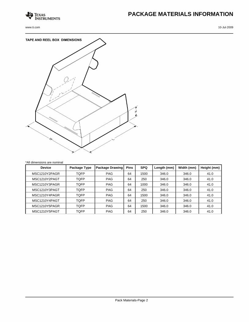
*All dimensions are nominal
Device Package Type Package Drawing Pins SPQ Length (mm) Width (mm) Height (mm)
MSC1210Y2PAGR TQFP PAG 64 1500 346.0 346.0 41.0
MSC1210Y2PAGT TQFP PAG 64 250 346.0 346.0 41.0
MSC1210Y3PAGR TQFP PAG 64 1000 346.0 346.0 41.0
MSC1210Y3PAGT TQFP PAG 64 250 346.0 346.0 41.0
MSC1210Y4PAGR TQFP PAG 64 1500 346.0 346.0 41.0
MSC1210Y4PAGT TQFP PAG 64 250 346.0 346.0 41.0
MSC1210Y5PAGR TQFP PAG 64 1500 346.0 346.0 41.0
MSC1210Y5PAGT TQFP PAG 64 250 346.0 346.0 41.0
PACKAGE MATERIALS INFORMATION
www.ti.com 10-Jul-2009
Pack Materials-Page 2

MECHANICAL DATA
MTQF006A – JANUARY 1995 – REVISED DECEMBER 1996
POST OFFICE BOX 655303 • DALLAS, TEXAS 75265
PAG (S-PQFP-G64) PLASTIC QUAD FLATPACK
0,13 NOM
0,25
0,450,75
Seating Plane
0,05 MIN
4040282/C 11/96
Gage Plane
33
0,170,27
16
48
1
7,50 TYP
49
64
SQ
9,80
1,050,95
11,8012,20
1,20 MAX
10,20SQ
17
32
0,08
0,50 M0,08
0°–7°
NOTES: A. All linear dimensions are in millimeters.B. This drawing is subject to change without notice.C. Falls within JEDEC MS-026

IMPORTANT NOTICETexas Instruments Incorporated and its subsidiaries (TI) reserve the right to make corrections, modifications, enhancements, improvements,and other changes to its products and services at any time and to discontinue any product or service without notice. Customers shouldobtain the latest relevant information before placing orders and should verify that such information is current and complete. All products aresold subject to TI’s terms and conditions of sale supplied at the time of order acknowledgment.TI warrants performance of its hardware products to the specifications applicable at the time of sale in accordance with TI’s standardwarranty. Testing and other quality control techniques are used to the extent TI deems necessary to support this warranty. Except wheremandated by government requirements, testing of all parameters of each product is not necessarily performed.TI assumes no liability for applications assistance or customer product design. Customers are responsible for their products andapplications using TI components. To minimize the risks associated with customer products and applications, customers should provideadequate design and operating safeguards.TI does not warrant or represent that any license, either express or implied, is granted under any TI patent right, copyright, mask work right,or other TI intellectual property right relating to any combination, machine, or process in which TI products or services are used. Informationpublished by TI regarding third-party products or services does not constitute a license from TI to use such products or services or awarranty or endorsement thereof. Use of such information may require a license from a third party under the patents or other intellectualproperty of the third party, or a license from TI under the patents or other intellectual property of TI.Reproduction of TI information in TI data books or data sheets is permissible only if reproduction is without alteration and is accompaniedby all associated warranties, conditions, limitations, and notices. Reproduction of this information with alteration is an unfair and deceptivebusiness practice. TI is not responsible or liable for such altered documentation. Information of third parties may be subject to additionalrestrictions.Resale of TI products or services with statements different from or beyond the parameters stated by TI for that product or service voids allexpress and any implied warranties for the associated TI product or service and is an unfair and deceptive business practice. TI is notresponsible or liable for any such statements.TI products are not authorized for use in safety-critical applications (such as life support) where a failure of the TI product would reasonablybe expected to cause severe personal injury or death, unless officers of the parties have executed an agreement specifically governingsuch use. Buyers represent that they have all necessary expertise in the safety and regulatory ramifications of their applications, andacknowledge and agree that they are solely responsible for all legal, regulatory and safety-related requirements concerning their productsand any use of TI products in such safety-critical applications, notwithstanding any applications-related information or support that may beprovided by TI. Further, Buyers must fully indemnify TI and its representatives against any damages arising out of the use of TI products insuch safety-critical applications.TI products are neither designed nor intended for use in military/aerospace applications or environments unless the TI products arespecifically designated by TI as military-grade or "enhanced plastic." Only products designated by TI as military-grade meet militaryspecifications. Buyers acknowledge and agree that any such use of TI products which TI has not designated as military-grade is solely atthe Buyer's risk, and that they are solely responsible for compliance with all legal and regulatory requirements in connection with such use.TI products are neither designed nor intended for use in automotive applications or environments unless the specific TI products aredesignated by TI as compliant with ISO/TS 16949 requirements. Buyers acknowledge and agree that, if they use any non-designatedproducts in automotive applications, TI will not be responsible for any failure to meet such requirements.Following are URLs where you can obtain information on other Texas Instruments products and application solutions:Products ApplicationsAmplifiers amplifier.ti.com Audio www.ti.com/audioData Converters dataconverter.ti.com Automotive www.ti.com/automotiveDLP® Products www.dlp.com Broadband www.ti.com/broadbandDSP dsp.ti.com Digital Control www.ti.com/digitalcontrolClocks and Timers www.ti.com/clocks Medical www.ti.com/medicalInterface interface.ti.com Military www.ti.com/militaryLogic logic.ti.com Optical Networking www.ti.com/opticalnetworkPower Mgmt power.ti.com Security www.ti.com/securityMicrocontrollers microcontroller.ti.com Telephony www.ti.com/telephonyRFID www.ti-rfid.com Video & Imaging www.ti.com/videoRF/IF and ZigBee® Solutions www.ti.com/lprf Wireless www.ti.com/wireless
Mailing Address: Texas Instruments, Post Office Box 655303, Dallas, Texas 75265Copyright © 2009, Texas Instruments Incorporated