Practical Sampling Issues
26
EECS 247- Lecture 17 Nyquist Rate ADCs-Sampling © 2008 H.K. Page 1 EE247 Lecture 17 • Nyquist rate ADC converters – Sampling • Sampling switch considerations –Thermal noise due to switch resistance (last lecture) –Clock jitter related non-idealities –Sampling switch bandwidth limitations –Switch induced distortion • Sampling switch conductance dependence on input voltage • Clock voltage boosters –Sampling switch charge injection & clock feedthrough EECS 247- Lecture 17 Nyquist Rate ADCs-Sampling © 2008 H.K. Page 2 Practical Sampling Issues v IN v OUT C M1 φ 1 • Switch induced noise due to M1 finite channel resistance • Clock jitter • Finite R sw limited bandwidth finite acquisition time • R sw = f(V in ) distortion • Switch charge injection & clock feedthrough
Transcript of Practical Sampling Issues

EECS 247- Lecture 17 Nyquist Rate ADCs-Sampling © 2008 H.K. Page 1
EE247Lecture 17
• Nyquist rate ADC converters– Sampling
• Sampling switch considerations–Thermal noise due to switch resistance (last lecture)–Clock jitter related non-idealities–Sampling switch bandwidth limitations–Switch induced distortion
• Sampling switch conductance dependence on input voltage
• Clock voltage boosters–Sampling switch charge injection & clock feedthrough
EECS 247- Lecture 17 Nyquist Rate ADCs-Sampling © 2008 H.K. Page 2
Practical SamplingIssues
vIN vOUT
CM1
φ1
• Switch induced noise due to M1 finite channel resistance• Clock jitter
• Finite Rsw limited bandwidth finite acquisition time
• Rsw = f(Vin) distortion• Switch charge injection & clock feedthrough

EECS 247- Lecture 17 Nyquist Rate ADCs-Sampling © 2008 H.K. Page 3
Clock Jitter
• The error voltage is
nominalsampling
time t0
actualsampling
time tJ
x(t)
x’(t0)
e = x’(t0)(tJ – t0)
error
EECS 247- Lecture 17 Nyquist Rate ADCs-Sampling © 2008 H.K. Page 4
Effect of Clock Jitter on Sampling of a Sinusoidal Signal
Sinusoidal input Worst case
78 ps0.24 ps0.3 ps
1 MHz20 MHz
1000 MHz
121610
dt <<fs# of Bits
sFSx
FSB 1
Bs
fAA f2 2
Ae( t )
2 2
1dt
2 fπ
+
= =
Δ<< ≅
<<
( )
( )
x
x
x x
xmax
max
x
Ampli tude: AFrequency: f J i t ter: d t
x( t ) Asin 2 f t
x' ( t ) 2 f Acos 2 f t
x' ( t ) 2 f A
Requirement:
e( t ) x' ( t ) dt
e( t ) 2 f Adt
π
π π
π
π
=
=
≤
≤
≤

EECS 247- Lecture 17 Nyquist Rate ADCs-Sampling © 2008 H.K. Page 5
Law of Jitter
• The worst case looks pretty stringent …what about the “average”?
• Let’s calculate the mean squared jitter error (variance)• If we’re sampling a sinusoidal signal
x(t) = Asin(2πfxt), then– x’(t) = 2πfxAcos(2πfxt)– E{[x’(t)]2} = 2π2fx2A2
• Assume the jitter has variance E{(tJ-t0)2} = τ2
EECS 247- Lecture 17 Nyquist Rate ADCs-Sampling © 2008 H.K. Page 6
Law of Jitter
• If x’(t) and the jitter are independent– E{[x’(t)(tJ-t0)]2}= E{[x’(t)]2} E{(tJ-t0)2}
• Hence, the jitter error power is
• If the jitter is uncorrelated from sample to sample, this “jitter noise” is white
E{e2} = 2π2fx2A2τ2

EECS 247- Lecture 17 Nyquist Rate ADCs-Sampling © 2008 H.K. Page 7
Law of Jitter
( )τπτπ
τπ
x
x
x
ff
AfADR
2log202
12
2/
10
222
2222
2
jitter
−=
=
=
EECS 247- Lecture 17 Nyquist Rate ADCs-Sampling © 2008 H.K. Page 8
Example: ADC Spectral Tests
SFDR
SDR
SNR
Ref: W. Yang et al., "A 3-V 340-mW 14-b 75-Msample/s CMOS ADC with 85-dB SFDR at Nyquist input," IEEE J. of Solid-State Circuits, Dec. 2001

EECS 247- Lecture 17 Nyquist Rate ADCs-Sampling © 2008 H.K. Page 9
More on Jitter• In cases where clock signal is provided from off-chip have to
choose a source with low enough jitter• On-chip precautions to keep the clock jitter less than single-digit
pico-second :– Separate supplies as much as possible– Separate analog and digital clocks– Short inverter chains between clock source and destination
• Few, if any, other analog-to-digital conversion non-idealities have the same symptoms as sampling jitter:– RMS noise proportional to input signal frequency– RMS noise proportional to input signal amplitude
In cases where clock jitter limits the dynamic range, it’s easy to tell, but may be difficult to fix...
EECS 247- Lecture 17 Nyquist Rate ADCs-Sampling © 2008 H.K. Page 10
Sampling Acquisition Bandwidth
• The resistance R of switch S1 turns the sampling network into a lowpass filter with finite time constant:
τ = RC
• Assuming Vin is constant during the sampling period and C is initially discharged
• Need to allow enough time for the output to settle to less than 1 ADC LSB determines minimum duration for φ1 or maximum clock frequency
vIN vOUT
CS1
φ1
R
( )τ/1)( tinout evtv −−=
φ1
vinvout
δ v

EECS 247- Lecture 17 Nyquist Rate ADCs-Sampling © 2008 H.K. Page 11
Sampling: Effect of Switch On-Resistance
Example:B = 14, C = 13pF, fs = 100MHzTs /τ >> 19.4, or 10τ <<Ts/2 R << 40 Ω
φ1
T=1/fS
tx
( )
( )
( )
/
2
since 11
2 ln
Worst Case:
1 0.722 ln 2 1
1 1 0.722 ln 2 1
s
tx tx tin out out in
Ts
inin
in FS
s sB
Bs s
V V V V eTV e or
V
V V
T TB
Rf C B f C
τ
τ τ
τ
−
−
− << Δ = −
→ << Δ <<⎛ ⎞⎜ ⎟Δ⎝ ⎠
=
×<< ≈−
<< ≈−
vIN vOUT
CS1
φ1
R
EECS 247- Lecture 17 Nyquist Rate ADCs-Sampling © 2008 H.K. Page 12
Switch On-Resistance
( ) ( )
( )
( )( )
0
1,2
1 1
1Let us call @ =0
1
DS
D triodeDSD triode ox GS TH DS
ON DS V
ON
ox GS th ox DD th in
in o o
ox DD th
oON
in
DD th
dIVWI C V V VL R dV
R W WC V V C V V VL L
R V R then R WC V VL
RR VV V
μ
μ μ
μ
→
⎛ ⎞= − − ≅⎜ ⎟⎝ ⎠
= =− − −
=−
=− −
Switch MOS operating in triode mode:
Vin
CM1
φ1 VDDVGS =VDD - Vin

EECS 247- Lecture 17 Nyquist Rate ADCs-Sampling © 2008 H.K. Page 13
Sampling Distortion
in
DD th
outT V12 V V
in
v
v 1 e τ
⎛ ⎞− −⎜ ⎟⎜ ⎟−⎝ ⎠
=⎛ ⎞⎜ ⎟−⎜ ⎟⎜ ⎟⎝ ⎠
Simulated 10-Bit ADC &Ts/2 = 5τVDD – Vth = 2V VFS = 1VSampling switch modeled:
Results in HD2=-41dBFS & HD3=-51.4dBFS
EECS 247- Lecture 17 Nyquist Rate ADCs-Sampling © 2008 H.K. Page 14
Sampling Distortion
10bit ADC Ts/2 = 10 τVDD – Vth = 2V VFS = 1V
Doubling sampling time (or ½time constant)Results in:
HD2 improved from -41dBFS to -70dBFS ~30dB
HD3 improved from -51.4dBFS to -76.3dBFS ~25dB
Allowing enough time for the sampling network settling Reduces distortion due to switch R non-linear behavior to a tolerable level

EECS 247- Lecture 17 Nyquist Rate ADCs-Sampling © 2008 H.K. Page 15
Sampling DistortionEffect of Supply Voltage
10bit ADC & Ts/2 = 5τVDD – Vth = 2V VFS = 1V
• Effect of higher supply voltage on sampling distortionHD3 decrease by (VDD1/VDD2)2
HD2 decrease by (VDD1/VDD2)
10bit ADC & Ts/2 = 5τVDD – Vth = 4V VFS = 1V
EECS 247- Lecture 17 Nyquist Rate ADCs-Sampling © 2008 H.K. Page 16
Sampling Distortion
10bit ADC Ts/τ = 20VDD – Vth = 2V VFS = 1V
• SFDR sensitive to sampling distortion - improve linearity by:
• Larger VDD /VFS ?Decreased dynamic range if VDD const.
• Larger switches?Issue:
Increased switchcharge injectionIncreased nonlinear
S &D junction cap.• Complementary switch• Constant & max.
VGS ≠ f(Vin)

EECS 247- Lecture 17 Nyquist Rate ADCs-Sampling © 2008 H.K. Page 17
Practical SamplingSummary So Far!
2
2212
B
BFS
C k TV
≥
( )1 for inON o o ox DD th
DD th
WVg g g C V VV V Lμ⎛ ⎞= − = −⎜ ⎟−⎝ ⎠
0.72
sR
B f C<<
• kT/C noise
• Finite Rsw limited bandwidth
• gsw = f (Vin) distortion
vINvOUT
CM1
φ1
EECS 247- Lecture 17 Nyquist Rate ADCs-Sampling © 2008 H.K. Page 18
Sampling: Use of Complementary Switches
φ1φ1B
φ1
φ1B
gon
gop
goT =go
n + gopgo
•Complementary n & p switch advantages:Increase in the overall conductanceLinearize the switch conductance for the range |Vth
p|< Vin < Vdd -|Vthn|

EECS 247- Lecture 17 Nyquist Rate ADCs-Sampling © 2008 H.K. Page 19
Complementary Switch IssuesSupply Voltage Evolution
• Supply voltage has scaled down with technology scaling• Threshold voltages do not scale accordingly
Ref: A. Abo et al, “A 1.5-V, 10-bit, 14.3-MS/s CMOS Pipeline Analog-to-Digital Converter,” JSSC May 1999, pp. 599.
EECS 247- Lecture 17 Nyquist Rate ADCs-Sampling © 2008 H.K. Page 20
Complementary SwitchEffect of Supply Voltage Scaling
gon
gop
goT =go
n + gopgeffective
•As supply voltage scales down input voltage range for constant go shrinksComplementary switch not effective when VDD becomes comparable to 2xVth
φ1φ1B
φ1
φ1B

EECS 247- Lecture 17 Nyquist Rate ADCs-Sampling © 2008 H.K. Page 21
Boosted & Constant VGS Sampling
VGS=const.
OFF ON
• Increase gate overdrive voltage as much as possible + keep VGSconstant
Switch overdrive voltage independent of signal level
Error due to finite RON linear (to 1st order)
Lower Ron lower time constant
• Gate voltage VGS =lowDevice offBeware of signal
feedthrough due to parasitic capacitors
EECS 247- Lecture 17 Nyquist Rate ADCs-Sampling © 2008 H.K. Page 22
Constant VGS Sampling
(= voltage @ the switch input terminal)

EECS 247- Lecture 17 Nyquist Rate ADCs-Sampling © 2008 H.K. Page 23
Constant VGS Sampling Circuit
VP1100ns
M12
M8
M9
M6
M11VS1
1.5V1MHz
Chold
P
C1 C2
M1 M2
VDD=3V
M3
C3
M5
M4
P
This Example: All device sizes: W/L=10μ/0.35μAll capacitor size: 1pF (except for Chold)
Note: Each critical switch requires a separate clock booster
P_N
Vg
Va Vb
Sampling switch & C
PB
Ref: A. Abo et al, “A 1.5-V, 10-bit, 14.3-MS/s CMOS Pipeline Analog-to-Digital Converter,” JSSC May 1999, pp. 599.
EECS 247- Lecture 17 Nyquist Rate ADCs-Sampling © 2008 H.K. Page 24
Clock Voltage Doubler
C1 C2
M10ff
M2Saturation
mode
VP1=clock
PB
VDD=0 3V
P
a) Start–up
0 3V
0 3V 0 0
0 3V 0 (3V-VthM2)
Acquire charge C1 C2
M1Triode
M2off
VP1
PB
VDD=3V
P
3V 0
3V 0
3V 0 3V (3V-VthM2) (6V-Vth
M2)
b) Next clock phase
0 3V

EECS 247- Lecture 17 Nyquist Rate ADCs-Sampling © 2008 H.K. Page 25
Clock Voltage Doubler
C1 C2
M10ff
M2
VP1
PB
VDD=3V
P
0 3V
0 3V
3V ~6V
3V 0
c) Next clock phase
(6V-VthM2) (3V-Vth
M2) ~ 3V
M2Triode
Acquires charge
• Both C1 & C2 charged to
VDD after one clock cycle
• Note that bottom plate of C1 & C2 is either 0 or VDD while top plates are at VDD or 2VDD
EECS 247- Lecture 17 Nyquist Rate ADCs-Sampling © 2008 H.K. Page 26
Clock Voltage Doubler
C1 C2
M1 M2
VP1Clock period: 100ns
PB
P_Boost
VDD
2VDD
0
VDD=3V
R1 R2
*R1 & R2=1GOhmdummy resistors added for simulation only
P

EECS 247- Lecture 17 Nyquist Rate ADCs-Sampling © 2008 H.K. Page 27
Constant VGS Sampler: Φ Low
• Sampling switch M11 is OFF
• C3 charged to ~VDDInput voltage
source
M3Triode
C3
M12Triode
M4
OFF
VS11.5V1MHz
Chold1pF
~ 2 VDD(boosted clock)
VDD
VDD
OFF M11OFF
DeviceOFF
VDD=3V
EECS 247- Lecture 17 Nyquist Rate ADCs-Sampling © 2008 H.K. Page 28
Constant VGS Sampler: Φ High
• C3 previously charged to VDD
• M8 & M9 are on:C3 across G-S of M11
• M11 on with constant VGS = VDD
C31pF
M8
M9 M11
VS11.5V1MHz
Chold
VDD

EECS 247- Lecture 17 Nyquist Rate ADCs-Sampling © 2008 H.K. Page 29
Constant VGS Sampling
Input Switch VGate
Input Signal
Chold Signal
EECS 247- Lecture 17 Nyquist Rate ADCs-Sampling © 2008 H.K. Page 30
Boosted Clock Sampling Complete Circuit
Ref: A. Abo et al, “A 1.5-V, 10-bit, 14.3-MS/s CMOS Pipeline Analog-to-Digital Converter,” JSSC May 1999, pp. 599.
Clock Multiplier
Switch
M13 added for reliability
Remaining issues:
-VGS constant only for Vin <Vout
- Nonlinearity due to Vth dependence of M11on body-source voltage
- Choice of size of C3 …..

EECS 247- Lecture 17 Nyquist Rate ADCs-Sampling © 2008 H.K. Page 31
Advanced Clock Boosting Technique
Ref: M. Waltari et al., "A self-calibrated pipeline ADC with 200MHz IF-sampling frontend," ISSCC 2002, Dig. Tech. Papers, pp. 314
Sampling Switch
EECS 247- Lecture 17 Nyquist Rate ADCs-Sampling © 2008 H.K. Page 32
Advanced Clock Boosting Technique
• clk low– Capacitors C1a & C1b charged to VDD– MS off– Hold mode
Sampling Switch
clk low

EECS 247- Lecture 17 Nyquist Rate ADCs-Sampling © 2008 H.K. Page 33
Advanced Clock Boosting Technique
Sampling Switch
• clk high– Top plate of C1a & C1b connected to gate of sampling switch– Bottom plate of C1a connected to VIN– Bottom plate of C1b connected to VOUT– VGS & VGD of MS both @ VDD & ac signal on G of MS average of VIN &
VOUT
clk high
EECS 247- Lecture 17 Nyquist Rate ADCs-Sampling © 2008 H.K. Page 34
Advanced Clock Boosting Technique
• Gate tracks average of input and output, reduces effect of I·R drop at high frequencies
• Bulk also tracks signal ⇒ reduced body effect (technology used allows connecting bulk to S)
• Reported measured SFDR = 76.5dB at fin=200MHz
Ref: M. Waltari et al., "A self-calibrated pipeline ADC with 200MHz IF-sampling frontend," ISSCC 2002, Dig. Tech. Papers, pp. 314
Sampling Switch

EECS 247- Lecture 17 Nyquist Rate ADCs-Sampling © 2008 H.K. Page 35
Constant Conductance Switch
Ref: H. Pan et al., "A 3.3-V 12-b 50-MS/s A/D converter in 0.6um CMOS with over 80-dB SFDR," IEEE J. Solid-State Circuits, pp. 1769-1780, Dec. 2000
EECS 247- Lecture 17 Nyquist Rate ADCs-Sampling © 2008 H.K. Page 36
Constant Conductance Switch
Ref: H. Pan et al., "A 3.3-V 12-b 50-MS/s A/D converter in 0.6um CMOS with over 80-dB SFDR," IEEE J. Solid-State Circuits, pp. 1769-1780, Dec. 2000
OFF

EECS 247- Lecture 17 Nyquist Rate ADCs-Sampling © 2008 H.K. Page 37
Constant Conductance Switch
Ref: H. Pan et al., "A 3.3-V 12-b 50-MS/s A/D converter in 0.6um CMOS with over 80-dB SFDR," IEEE J. Solid-State Circuits, pp. 1769-1780, Dec. 2000
ON
M2 Constant currentconstant gds
M1 replica of M2 & same VGSas M2M1 alsoconstant gds
• Note: Authors report requirement of 280MHz GBW for the opamp for 12bit 50Ms/s ADC
• Also, opamp common-mode compliance for full input range required
EECS 247- Lecture 17 Nyquist Rate ADCs-Sampling © 2008 H.K. Page 38
Switch Off-Mode Feedthrough Cancellation
Ref: M. Waltari et al., "A self-calibrated pipeline ADC with 200MHz IF-sampling frontend," ISSCC 2002, Dig. Techn. Papers, pp. 314

EECS 247- Lecture 17 Nyquist Rate ADCs-Sampling © 2008 H.K. Page 39
Practical Sampling
Vo
CM1
φ1
• Rsw = f(Vi) distortion• Switch charge injection & clock feedthrough
Vi
EECS 247- Lecture 17 Nyquist Rate ADCs-Sampling © 2008 H.K. Page 40
Sampling Switch Charge Injection & Clock FeedthroughSwitching from Track to Hold
Vi VO
Cs
M1
VG
• First assume Vi is a DC voltage• When switch turns off offset voltage induced on Cs• Why?
VG
t
VH
Vi
VL
Vi +Vth
VO
Vi
toff
ΔV
t

EECS 247- Lecture 17 Nyquist Rate ADCs-Sampling © 2008 H.K. Page 41
SamplingSwitch Charge Injection
• Channel distributed RC network formed between G,S, and D• Channel to substrate junction capacitance distributed & voltage dependant• Drain/Source junction capacitors to substrate voltage dependant• Over-lap capacitance Cov = LDxWxCox
’ associated with G-S & G-D overlap
MOS xtor operating in triode regionCross section view
Distributed channel resistance & gate & junction capacitances
S
G
D
B
LD
L
Cov Cov
Cjdb
Cjsb
CHOLD
EECS 247- Lecture 17 Nyquist Rate ADCs-Sampling © 2008 H.K. Page 42
Switch Charge Injection Slow Clock
• Slow clock clock fall time >> device speed During the period (t- to toff) current in channel discharges channel charge into low impedance signal source
• Only source of error Clock feedthrough from Cov to Cs
VG
t
VH
Vi
VL
Vi +Vth
tofft-
Device still conducting

EECS 247- Lecture 17 Nyquist Rate ADCs-Sampling © 2008 H.K. Page 43
Switch Clock Feedthrough Slow Clock
VG
t
VH
Vi
VL
Vi +Vth
VO
Vi
toff
ΔV
t
D
Cov
VG
t-
Cs( )
( )
( ) ( )
( )
( )
ovi th L
ov sov
i th Ls
o i
ov ov ovo i i th L i th L
s s so i os
ov ovos th L
s s
CV V V V
C CC
V V VC
V V VC C C
V V V V V V 1 V VC C C
V V 1 V
C Cwhere ; V V V
C C
ε
ε
Δ = − + −+
≈ − + −
= + Δ⎛ ⎞
= − + − = − − −⎜ ⎟⎜ ⎟⎝ ⎠
= + +
= − = − −
EECS 247- Lecture 17 Nyquist Rate ADCs-Sampling © 2008 H.K. Page 44
Switch Charge Injection & Clock Feedthrough Slow Clock- Example
VG
t
VH
Vi
VL
Vi +Vth
VO
Vi
toff
ΔV
t
Vi VO
Cs=1pF
M1
VG 10μ/0.18μ
t-
( )
' 2ov ox th L
ov
s
ovos th L
s
C 0.1 fF / C 9 fF / V 0.4V V 0
C 10 x0.1 fF /.1%
C 1pFAllowing 1 / 2LSB ADC resolut ion ~ 9bi t
CV V V 0.4mV
C
μ μ
μ με
ε
= = = =
= − = − = −
= → <
= − − = −
EECS 247- Lecture 17 Nyquist Rate ADCs-Sampling © 2008 H.K. Page 45
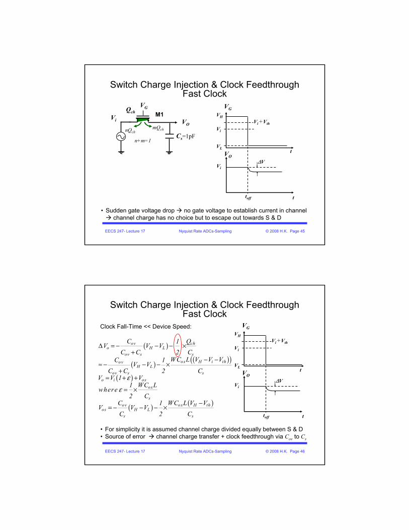
Switch Charge Injection & Clock Feedthrough Fast Clock
VG
t
VH
Vi
VL
Vi +Vth
VO
Vi
toff
ΔV
t
Vi VO
Cs=1pF
M1VG
• Sudden gate voltage drop no gate voltage to establish current in channel channel charge has no choice but to escape out towards S & D
Qch
mQchnQch
n+m=1
EECS 247- Lecture 17 Nyquist Rate ADCs-Sampling © 2008 H.K. Page 46
• For simplicity it is assumed channel charge divided equally between S & D • Source of error channel charge transfer + clock feedthrough via Cov to Cs
VG
t
VH
Vi
VL
Vi +Vth
VO
Vi
toff
ΔV
t
Switch Charge Injection & Clock FeedthroughFast Clock
Clock Fall-Time << Device Speed:
( )
( ) ( )( )
( )
( ) ( )
ov cho H L
ov s s
ox H i thovH L
ov s so i os
ox
sox H thov
os H Ls s
C 1 QV V V
C C 2 CWC L V V VC 1
V VC C 2 C
V V 1 V1 WC L
where2 C
WC L V VC 1V V V
C 2 C
ε
ε
Δ = − − − ×+
− −≈ − − − ×
+= + +
= ×
−= − − − ×

EECS 247- Lecture 17 Nyquist Rate ADCs-Sampling © 2008 H.K. Page 47
Switch Charge Injection & Clock FeedthroughFast Clock- Example
Vi VO
Cs=1pF
M1
VG 10μ/0.18μ
( ) ( )
ov ox th DD L2
2ox
s
ox H thovos H L
s s
fF fFC 0.1 , C 9 , V 0.4V ,V 1.8V , V 0
WLC 10 x0.18 x9 fF /1 / 2 1.6% ~ 5 bi t
C 1pF
WC L V VC 1V V V 1.8mV 14.6mV 16.4mV
C 2 C
μ μμ μ με
= = = = =
= = = → −
−= − − − × = − − = −
VG
t
VH
Vi
VL
Vi +Vth
VO
Vi
toff
ΔV
t
EECS 247- Lecture 17 Nyquist Rate ADCs-Sampling © 2008 H.K. Page 48
Vo
ΔV
Vi
Switch Charge Injection & Clock FeedthroughSlow Clock versus Fast Clock
Slow Clock
Vo
ΔV
Vi
Fast Clock

EECS 247- Lecture 17 Nyquist Rate ADCs-Sampling © 2008 H.K. Page 49
Switch Charge Injection & Clock FeedthroughExample-Summary
Error function of:Clock fall time Input voltage level Source impedance Sampling capacitance size Switch size
Clock fall/rise should be controlled not to be faster (sharper) than necessary
Clock fall time
ε VOS
Clock fall time
1.6%
.1%
16mV
0.4mV
EECS 247- Lecture 17 Nyquist Rate ADCs-Sampling © 2008 H.K. Page 50
Switch Charge InjectionError Reduction
• How do we reduce the error? Reduce switch size to reduce channel charge?
Reducing switch size increases τ increased distortion not a viable solutionSmall τ and small ΔV use minimum chanel length (mandated by technology)For a given technology τ x ΔV ~ constant
( )
( )
( )( )
cho
ss s
ON s
ox GS th
ox GS ths
o s ox H i th2
1 QV
2 CC T
R C ( note : kW 2C V VL
Consider the f igure of meri t (FOM):W
C V V1 CLFOM 2V C WC L V V V
FOM L
)μ
μ
μ
τ τ
τ
Δ = − ↓
= = ↑ =−
−= ≈ ×
Δ − −→ ∝
××

EECS 247- Lecture 17 Nyquist Rate ADCs-Sampling © 2008 H.K. Page 51
Sampling Switch Charge Injection & Clock FeedthroughSummary
• Extra charge injected onto sampling capacitor @ switch device turn-off
–Channel charge injection–Clock feedthrough to Cs via Cov
• Issues due to charge injection & clock feedthrough:–DC offset induced on hold C–Input dependant error voltage distortion
• Solutions:–Complementary switch?–Addition of dummy switches?–Bottom-plate sampling?