Power-supply device
23
US 20050029997A1 (12) Patent Application Publication (10) Pub. No.: US 2005/0029997 A1 (19) United States Sase et al. (43) Pub. Date: Feb. 10, 2005 (54) POWER-SUPPLY DEVICE (30) Foreign Application Priority Data (76) Inventors: Takashi Sase, Hitachi (JP); Koji Jun. 17, 2002 (JP) .................................... .. 2002-175172 Tateno, Hitachi (JP); Akihiko Kanouda, Hitachinaka (JP); Katsunori Hayashi, OdaWara (JP); Shinichi Yoshida, Takasaki (JP) Correspondence Address: ANTONELLI, TERRY, STOUT & KRAUS, LLP 1300 NORTH SEVENTEENTH STREET SUITE 1800 ARLINGTON, VA 22209-9889 (US) (21) Appl. No.: 10/937,397 (22) Filed: Sep. 10, 2004 Related US. Application Data (63) Continuation of application No. 10/462,680, ?led on Jun. 17, 2003, noW Pat. No. 6,798,180. Publication Classi?cation (51) Int. Cl? ..................................................... .. G05F 1/40 (52) Us. 01. ............................................................ ..323/282 (57) ABSTRACT A step-down type DC-DC power-supply device implements both the stabilization of the control loop and the responsi bility at the same time. In the power-supply device, an output poWer signal is fed back to an error ampli?er after having passed through a CR smoothing ?lter provided independently of a poWer LC smoothing ?lter. Also, inde pendently of the duty controls over PoWer MOSFETs, i.e., upper-side/loWer-side semiconductor sWitching components in the steady state, an output from the poWer LC smoothing ?lter is added to an upper and loWer limit-mode-equipped control circuit, thereby, at the transient state, forcefully setting the duty 0t at either 0% or 100%. PW VFB __ EA 3 ‘M _ Ell“ Vref + ' DRV
Transcript of Power-supply device

US 20050029997A1
(12) Patent Application Publication (10) Pub. No.: US 2005/0029997 A1 (19) United States
Sase et al. (43) Pub. Date: Feb. 10, 2005
(54) POWER-SUPPLY DEVICE (30) Foreign Application Priority Data
(76) Inventors: Takashi Sase, Hitachi (JP); Koji Jun. 17, 2002 (JP) .................................... .. 2002-175172 Tateno, Hitachi (JP); Akihiko Kanouda, Hitachinaka (JP); Katsunori Hayashi, OdaWara (JP); Shinichi Yoshida, Takasaki (JP)
Correspondence Address: ANTONELLI, TERRY, STOUT & KRAUS, LLP 1300 NORTH SEVENTEENTH STREET SUITE 1800 ARLINGTON, VA 22209-9889 (US)
(21) Appl. No.: 10/937,397
(22) Filed: Sep. 10, 2004
Related US. Application Data
(63) Continuation of application No. 10/462,680, ?led on Jun. 17, 2003, noW Pat. No. 6,798,180.
Publication Classi?cation
(51) Int. Cl? ..................................................... .. G05F 1/40
(52) Us. 01. ............................................................ ..323/282
(57) ABSTRACT
A step-down type DC-DC power-supply device implements both the stabilization of the control loop and the responsi bility at the same time. In the power-supply device, an output poWer signal is fed back to an error ampli?er after having passed through a CR smoothing ?lter provided independently of a poWer LC smoothing ?lter. Also, inde pendently of the duty controls over PoWer MOSFETs, i.e., upper-side/loWer-side semiconductor sWitching components in the steady state, an output from the poWer LC smoothing ?lter is added to an upper and loWer limit-mode-equipped control circuit, thereby, at the transient state, forcefully setting the duty 0t at either 0% or 100%.
PW VFB __ EA 3 ‘M
_ Ell“ Vref + '
DRV
Patent Application Publication Feb. 10, 2005 Sheet 1 0f 14 US 2005/0029997 A1
FIG.1
VFB t. EA PV‘I’M _ PWM
Vref 08C‘

Patent Application Publication Feb. 10, 2005 Sheet 2 0f 14 US 2005/0029997 A1
V0
C
Vx
EA /////////////////4
//// VIIIIIIII/l/l
n v 7//////////////. A
DRV PWM /
PWM OSC
PWM OSC
Patent Application Publication Feb. 10, 2005 Sheet 3 0f 14 US 2005/0029997 A1
Vi PWM
VFB _,. EA 1 DRV
PWM Vref osc.
\f -L— . WD 7
3o / _‘_yref+A in?'i‘e‘w'iNJ A |
3100 DETECTION
Vo
K Vref- A
Patent Application Publication Feb. 10, 2005 Sheet 4 0f 14 US 2005/0029997 A1
+
|NV5 b ~INV1
CMP2 '------------ ---
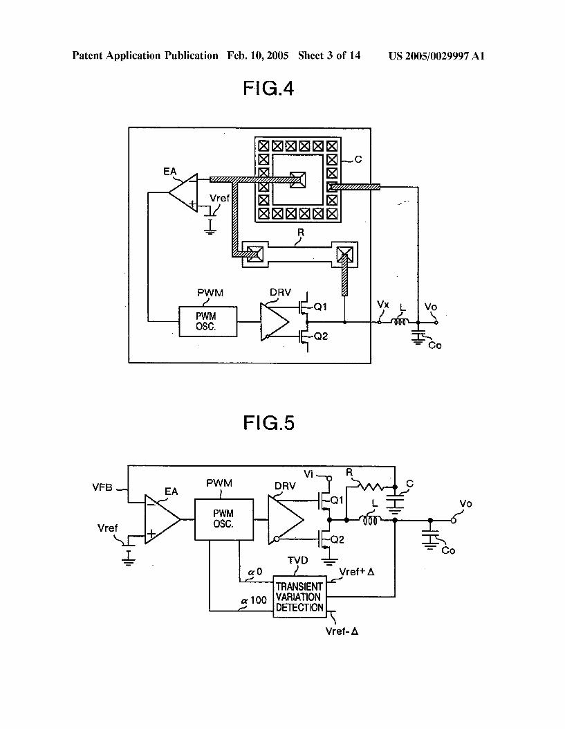
Patent Application Publication Feb. 10, 2005 Sheet 5 0f 14 US 2005/0029997 A1
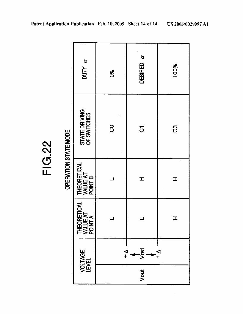
OPERATION STATE MODE
THEORETICAL THEORETICAL VOLTAGE LEVEL VALUE AT VALUE AT ggg?ggl'yé'é‘a DUTY a
POINTA POINTB
SW1, 4 : on‘ |_ |_ ~ 0%
SW2, 3 ; off +A i
Vout Vr+ef L H SW1~4 : all off DESIRED a
-A
sw1, 4:0ff H H 100%
SW2, 3 :on
Vi
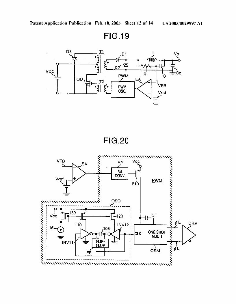
VFB _. EA P‘AIIM DRV _ Vo
PWM Vref A + 080.
\_|_— J:- TVD
a0 / ,1
TiAusllEmT - v RIAT
510° DEIECTION
Vref- A

Patent Application Publication Feb. 10, 2005 Sheet 6 0f 14 US 2005/0029997 A1
v Vi
VFB _._ PV‘I'M DRV V0
vPWM
Vref \J__ ~'
@- TVD‘ a: 0 / /
iiéi??? 310° DETECTION K
Vref-A
' PWM vi DRV
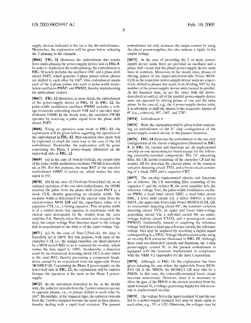
Vo PWM
Vref 080.
\L -__L TVD
a O / /
TRANSIEONT 100 VARIATI N 5 DETECTION
Vref- A
Patent Application Publication Feb. 10, 2005 Sheet 7 0f 14
F|G.11
US 2005/0029997 A1
Vi
PVXMT DRV VFB1\ EA1
—CLK ' V°
Vref / HST \_l__ TVD1 l 5.0 /
osc : PSFT TRANSIENT
/ / game 03 - ,1
0S0 _ PHASE _ _ Vref-A
SHIFT _
Vi PWM2 DRV2
VFB2\ E A2 / ' ' — CLK
Vref + RST
*5 we a '0 = ” TRANSIENT C4
@1100 VARIATION / DETECTION xvref A

Patent Application Publication Feb. 10, 2005 Sheet 8 0f 14 US 2005/0029997 A1
_______ ....n’...__....____..___ l
i
VFB1 i \ n - . _ _ — - - - - - Q - - - - - - - - - - - -
l_'__ EA1 Vcc VII I M21 CONV. E J i
+ / 210' 0R1 W11 0;;
CT1"__ '
HST /
Phase1 CLK OSC PSFT ONE-SHOT MULTI. ’
/ / / 08C. __ PHASE || || || OSM1
SH|FT Tm- OSM2 / Vref ONE-SHOT MULTI. I
01/ Phase2 CLK 95 LL’; =2 RST 9*» ' GT2 0R2
EA2 W12 92 + / 210 4
VII I _ _ CONV. $121‘
I— Vcc \ VFB2 ‘ I. ..... “4-: ____________ __
. w : 4:
l I

Patent Application Publication Feb. 10, 2005 Sheet 9 0f 14 US 2005/0029997 A1
OPERATION STATE MODE
- THEORETICAL THEORETICAL
{$265 VALUE AT VALUE AT gPg?RgIYg'g'G ou‘w 0: POINT A POINT B
‘ITA L ' |_ RST 0%
- CLK TRIGGER-PULSE ' .
' SHORT-CIRCUIT
_ A H H OF CT 100%
gf? "/8 (D _I_ II M Q_ 'P-"O
(‘O a:
‘—LEF-—J\@ N Q 0
<1‘ \ W2 ‘'1 c:
L5 2
>I<~ oaog cg - .: E? égasrg I


Patent Application Publication Feb. 10, 2005 Sheet 11 0f 14 US 2005/0029997 A1
FIG.1 7
BGA L C0
1 2 k 2 0-0.’: ’ E|_|S (I I)
~PB
FlG.‘l8'
DC-DC1 DC-DC2 DC-DC3 DC-DCn LINE } ) 1 ) \ / / / /
I! I I | I ‘I
DC-DC DG-DC DC-DC ______ _ _ DC-DC CONV. CONV. CONV. CONV.
V V V >
f / f / HDD1 HDD2 HDD3 HDDn
Patent Application Publication Feb. 10, 2005 Sheet 12 0f 14 US 2005/0029997 A1
FIG.19
D1 '- v0
02 “I ‘I\ VD ' R’ \ 3=—Co
PWM c EA \
PWM - VFB
036- ' Vref
\\\\\\\\\\\\\\\\\\\\\\\\\\\\\\\\ VFB V /| Vcc
EA f,
VII I 'CONV,
PWM 21 0 —
L
//////////l Ill/lll////////////////////////////// S f """"""""""""""""""" "
‘ 130
s i Vcc FLTT \ : L s i 15 ‘ 2 DRV S : i CLK ONE SHOT t 5 _ MULTI \ I _
§ : |N\_/11 8 5 \ : ¢L § : OSM
Ea ..................................... _ §\\\\\\\\\\\\\\\\\\\\\\\\\\\\\\\\\\\\\\\\\\\\\\\\\\\\\\\\

Patent Application Publication Feb. 10, 2005 Sheet 14 0f 14 US 2005/0029997 A1
$82 no . I I
4
. .q omEmwo 6 I . I. h2+> 50>
4+
$0 00 |_ |_
a so omwh?? mug moo: w._.<._.w zo_._.<mmn_o NNG _ u_
US 2005/0029997 A1
POWER-SUPPLY DEVICE
BACKGROUND OF THE INVENTION
[0001] 1. Field of the Invention
[0002] The present invention relates to a poWer-supply device Where, independently of a power LC smoothing ?lter, a signal is caused to pass through a CR smoothing ?lter and is then fed back so that the control loop Will be stabiliZed.
[0003] 2. Description of the Related Art
[0004] A prior art on the loop stabilizing method for a poWer-supply device has been described in “Low-Voltage On-Board DC/DC Modules for Next Generations of Data Processing Circuits”, Zhang et al., IEEE Tran. on PoWer Elect. Vol. 11, No. 2, March 1996. In the poWer-supply device according to the prior art, a signal is fed back to an error ampli?er from a poWer LC smoothing ?lter. Then, the error ampli?er compensates the phase, thereby implement ing the stabiliZation of the control loop. In this prior art, an aluminum electrolytic capacitor is used as the poWer LC smoothing ?lter.
[0005] US. Pat. No. 5,877,611 discloses a poWer supply system in Which an output of a CR smoothing ?lter con nected across an inductor of an output LC smoothing ?lter is fed back to an error ampli?er having a loW input imped ance. In the US. patent prior art, voltage and current signals of a poWer supply output are extracted using the CR smooth ing ?lter, so that the resistance value of the CR smoothing ?lter must be set to be small. The component constants of the CR smoothing ?lter are a capacitance of 0.47 MF and a resistance of 100 Q. Accordingly, the CR smoothing ?lter having such constants cannot be formed on chip in a poWer supply IC and must be formed externally of the IC chip, resulting in a problem that the poWer supply device cannot be made in small siZe totally.
SUMMARY OF THE INVENTION
[0006] In order to doWnsiZe the poWer-supply device, instead of using the aluminum electrolytic capacitor as the poWer LC smoothing ?lter, there has occurred a necessity for using a ceramic capacitor of a chip-part as the poWer LC smoothing ?lter. HoWever, the equivalent series resistance (ESR) of the chip ceramic capacitor is equal to several mQ, Which is considerably small. What is more, the ceramic capacitors are connected in parallel under an actual use condition. Accordingly, the total of the ESRs in this case becomes less than 1 m9, Which is even smaller. This makes it impossible to expect the damping of the ESR as is expected in the case of using the aluminum electrolytic capacitor. Consequently, it becomes difficult to stabiliZe the control loop.
[0007] In the above-described prior art, When using the ceramic capacitor With the small ESR as the poWer LC smoothing ?lter, it becomes impossible to expect the damp ing effect of the ESR. This causes a signal to oscillate, thereby making the phase compensation difficult. Also, if, in the prior art, it Were to become possible to implement the phase compensation by narroWing the operation bandWidth of the error ampli?er, a response from the poWer-supply is delayed exceedingly. Moreover, in modifying the LC smoothing ?lter’s constants, there exists a troublesome task
Feb. 10, 2005
of adjusting the phase compensation condition of the error ampli?er on each that occasion.
[0008] It is an object of the present invention to provide a poWer-supply device that employs a novel control method Where, independently of a poWer LC smoothing ?lter, a signal is caused to pass through a CR smoothing ?lter and is then fed back so that the control loop Will be stabiliZed.
[0009] ApoWer-supply device according to one aspect of the present invention is as folloWs: In the control loop of the poWer-supply device of a step-doWn type DC-DC converter, a CR smoothing ?lter is provided independently of a poWer LC smoothing ?lter. Moreover, a signal corresponding to the output poWer is fed back to an error ampli?er after having passed through the CR smoothing ?lter.
[0010] Also, a poWer-supply device according to another aspect of the present invention includes the folloWing unit: Independently of the duty controls over PoWer MOSFETs, i.e., upper-side/loWer-side semiconductor sWitching compo nents in the steady state, the unit adds the output from a poWer LC smoothing ?lter to an upper and loWer limit value detecting circuit, thereby, at the transient state, forcefully setting the duty at either 0% or 100%.
[0011] Moreover, a poWer-supply device according to still another aspect of the present invention is as folloWs: The poWer-supply device includes poWer-supply device units prepared in plural number. In order to perform a parallel operation of these poWer-supply device units, the poWer supply device further includes an oscillator and a phase shift circuit that the plural poWer-supply device units have in common. Furthermore, in the steady state, phases of driving pulses of upper-side/loWer-side PoWer MOSFETs in the respective poWer-supply device units are respectively shifted to phases that result from dividing 360° by the number of the parallelism. At the transient state, all of the parallel poWer-supply device units are operated by driving pulses of one and the same phase.
[0012] Other objects, features and advantages of the invention Will become apparent from the folloWing descrip tion of the embodiments of the invention taken in conjunc tion With the accompanying draWings.
BRIEF DESCRIPTION OF THE DRAWINGS
[0013] FIG. 1 is a circuit block diagram for illustrating a poWer-source device of a ?rst embodiment in the present invention; [0014] FIG. 2 is an explanatory diagram for explaining an IC Where a CR ?lter is built in a semiconductor chip in the poWer-supply device in FIG. 1;
[0015] FIG. 3 is a circuit block diagram for illustrating a poWer-supply device of a second embodiment in the present invention; [0016] FIG. 4 is an explanatory diagram for explaining an IC Where a CR ?lter is built in a semiconductor chip in the poWer-supply device in FIG. 3;
[0017] FIG. 5 is a circuit block diagram for illustrating a poWer-supply device of a third embodiment in the present invention; [0018] FIG. 6 is a circuit diagram for illustrating the details in FIG. 5;

US 2005/0029997 A1
[0019] FIG. 7 is a diagram for illustrating the operation state mode in FIG. 6;
[0020] FIG. 8 is a circuit block diagram for illustrating a poWer-supply device of a fourth embodiment in the present invention; [0021] FIG. 9 is a circuit block diagram for illustrating another poWer-supply device of the fourth embodiment;
[0022] FIG. 10 is a circuit block diagram for illustrating still another poWer-supply device of the fourth embodiment;
[0023] FIG. 11 is a circuit block diagram for illustrating a multi-phase poWer-source device of a ?fth embodiment in the present invention;
[0024] FIG. 12 is a circuit diagram for illustrating the details in FIG. 11;
[0025] FIG. 13 is a diagram for illustrating the operation state mode in FIG. 12;
[0026] FIG. 14 is a circuit block diagram for illustrating an example of the chip con?guration of a poWer-source device of a sixth embodiment in the present invention;
[0027] FIG. 15 is an explanatory diagram for explaining a VID code input D/A converter applied to FIG. 14;
[0028] FIG. 16 is a circuit block diagram for illustrating a multi-phase compatible chip of a seventh embodiment in the present invention;
[0029] FIG. 17 is an explanatory diagram for explaining the printed Wiring board implementation of a poWer-source control IC of an eighth embodiment;
[0030] FIG. 18 is an explanatory diagram for explaining a HDD device of a ninth embodiment;
[0031] FIG. 19 is an explanatory diagram for explaining a tenth embodiment in the present invention;
[0032] FIG. 20 is an explanatory diagram for illustrating another embodiment of a pulse-Width modulation oscillator PWM;
[0033] FIG. 21 is an explanatory diagram for explaining an eleventh embodiment in the present invention applied to a commercially-available poWer-source IC; and
[0034] FIG. 22 is a diagram for illustrating the operation state mode in FIG. 21.
DETAILED DESCRIPTION OF THE EMBODIMENTS
[0035] Referring to the accompanying draWings, the explanation Will be given beloW concerning the details of the present invention.
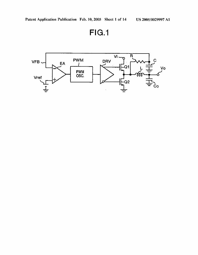
[0036] Embodiment 1
[0037] FIG. 1 illustrates a poWer-supply device of the present embodiment. In FIG. 1, reference notations Vi and V0 denote an input terminal and an output terminal, respec tively. An upper-side PoWer MOSFET Q1 is connected to the input terminal Vi, and a loWer-side PoWer MOSFET Q2 is connected to a ground potential side. An LC smoothing ?lter, i.e., a poWer output ?lter consisting of an inductor L and a capacitor C0, and a CR smoothing ?lter consisting of a resistor R and a capacitor C are connected in parallel to a
Feb. 10, 2005
midpoint of the PoWer MOSFETs Q1 and Q2. Moreover, the output terminal V0 is connected to a midpoint of the LC smoothing ?lter, and one input (—) of an error ampli?er EA is connected to a midpoint of the CR smoothing ?lter. Here, the capacitor C0 of the LC smoothing ?lter is a chip ceramic capacitor. [0038] Also, a reference voltage Vref is connected to the other input (+) of the error ampli?er EA. A pulse-Width modulation (abbreviated as PWM) oscillator PWM, and gates of the PoWer MOSFETs Q1 and Q2 via a driver DRV are connected to an output of the error ampli?er EA. The PoWer MOSFETs Q1 and Q2 are driven in opposite phases to each other, and thus are electrically conducted alternately. In the present embodiment, an output voltage Vout is smaller than an input voltage Vin.
[0039] Next, the explanation Will be given beloW regard ing the circuit operation in FIG. 1. The input voltage Vin applied to the input terminal Vi is converted into a voltage by on/off controls over the upper-side PoWer MOSFET Q1 and the loWer-side PoWer MOSFET Q2 via the CR smooth ing ?lter. This converted voltage VFB is compared With the reference voltage Vref by the error ampli?er EA. As a consequence, an error voltage is generated in a state of being ampli?ed at the output of the error ampli?er EA. This error voltage is converted into a PWM pulse by the pulse-Width modulation oscillator PWM. This PWM pulse is further converted by the driver DRV into an on/off-time ratio (i.e., duty: 0t) at Which the driver DRV drives the upper-side PoWer MOSFET Q1 and the loWer-side PoWer MOSFET Q2. Moreover, a negative-feedback control is performed over the PWM pulse so that the error voltage becomes equal to 0. As a result of this, the converted voltage VFB becomes equal to the reference voltage Vref. In this case, the con verted voltage VFB acquired through the CR smoothing ?lter in the steady state is proportional to the duty 0t of the input voltage Vin. Consequently, the folloWing relational expression holds:
[0040] Where the duty 0t assumes a value in the range of 0 to 1, since 0t is de?ned as the on-time/(a total of the on-time and the off-time).
[0041] In the case of the ordinary step-doWn type con verter, it has been found out that the voltage-converted ratio in the steady state is equal to the ratio, i.e., the duty, betWeen the output voltage and the input voltage. Accordingly, assuming that the input voltage is Vin and the duty is ot, the output from the LC smoothing ?lter, i.e., the output voltage Vout acquired at the output terminal Vo, can be determined by a relational expression:
[0042] From the above-described 2 expressions, the fol loWing relational expression holds:
[0043] Consequently, even if no direct negative-feedback control is performed over the output from the LC smoothing ?lter, if an indirect control over the duty 0t using some other method proves successful, this successful indirect control becomes equivalent to a direct control over the output voltage Vout at the output terminal Vo. As a result, it becomes possible to acquire, at the output terminal Vo, the voltage that is proportional to the duty 0t of the input voltage

US 2005/0029997 A1
Vin. In other Words, the Power MOSFETs Q1 and Q2 are driven, thereby performing the negative-feedback control over the output from the CR smoothing ?lter. This operation allows the desired voltage, Which is proportional to the duty 0t of the input voltage Vin, to be also acquired at the output from the LC smoothing ?lter as the output voltage Vout.
[0044] As the voltage converting method based on the duty control over the upper-side PoWer MOSFET Q1 and the loWer-side PoWer MOSFET Q2, the present embodiment is a primary-delay control method Where the CR smoothing ?lter is used for the control loop. Accordingly, since there exists none of the secondary delay by the LC smoothing ?lter as Was found in the prior art, the control loop does not become the oscillating system. This prevents the oscillating Waveform from occurring in the output, thereby making the loop stable. Consequently, according to the present embodi ment, even if the chip ceramic capacitor With a small ESR is used as the capacitor of the LC smoothing ?lter, it is possible to stabiliZe the control loop.
[0045] Next, the explanation Will be given beloW concern ing the large-or -small relationship among the corner fre quencies and the sWitching frequency of the above-de scribed 2 smoothing ?lters. Let’s assume that the corner frequency of the CR smoothing ?lter and that of the LC smoothing ?lter are equal to fCR and fLC respectively, and that the sWitching frequency is equal to fSW. Then, setting the relationship among these frequencies as fLC<fCR<fSW makes it possible to ensure the stability of the loop. More over, from this relationship, the feedback from the CR smoothing ?lter results in a higher operation frequency as compared With the feedback from the LC smoothing ?lter, Which alloWs the implementation of the high-speed response. Also, fLC and fCR are set as frequencies that are different to some extent. This setting, even if the LC smoothing ?lter’s constants are modi?ed, makes it unnec essary to change the CR smoothing ?lter’s constants, thereby alloWing an increase in the degree-of-freedom of the design. With respect to the high-speed operation of a 1-to 6-MHZ sWitching frequency, values usable as the LC smoothing ?lter’s constants and the CR smoothing ?lter’s constants are, e.g., 0.2 pH, 220 pF, and 20 ME, 200 kQ, respectively. If the values of these capacitors and this resistor are of these orders, it becomes possible to mount (i.e., on-chip) the CR smoothing ?lter on a semiconductor integrated circuit chip, thereby making externally-attached components unnecessary. This means the folloWing: By merely replacing the poWer-supply device illustrated in FIG. 1 by an IC Whose terminal location is the same (i.e., pin-compatible) as that of the poWer-supply control IC in the prior art, the printed Wiring board in the prior art can be utiliZed With no modi?cation added thereto.
[0046] FIG. 2 is an explanatory diagram for explaining the chip layout in the case Where, in the poWer-supply device in FIG. 1, the CR smoothing ?lter is built in a semiconduc tor chip. In FIG. 2, reference notations C and R denote a built-in capacitor and a built-in resistor, respectively. These components are mounted on a semiconductor board that is the same as the one that mounts thereon the error ampli?er EA, the pulse-Width modulation oscillator PWM, the driver DRV, and the PoWer MOSFETs Q1 and Q2.
[0047] So far, the explanation has been given selecting, as the example, the CR smoothing ?lter Whose output is fed
Feb. 10, 2005
back to the error ampli?er in the control loop. Instead of the CR smoothing ?lter, hoWever, the use of another high response ?lter circuit alloWs the acquisition of basically the same effects. Also, although the explanation has been given selecting the PoWer MOSFETs as the example of the semi conductor sWitching components, the IGBTs may be used instead.
[0048] Embodiment 2
[0049] FIG. 3 illustrates the present embodiment. In FIG. 3, the same reference notations are attached to the same con?guration components in FIG. 1. The point in Which FIG. 3 differs from FIG. 1 is that the CR smoothing ?lter is set up at both ends of the inductor L of the LC smoothing ?lter. In the present embodiment, since the electrostatic capacitance of the capacitor C0 of the output LC smoothing ?lter is large, the inductor-connected edge side of the capacitor C0 can also be regarded as the ground potential. The present embodiment also alloWs the acquisition of basically the same effects in FIG. 1. Furthermore, the present embodiment makes it possible to perform the nega tive feedback of an in?nitesimal capacitance change caused by a temperature change in the capacitor C0 of the LC smoothing ?lter. Consequently, even if the chip ceramic capacitor With a small ESR is used, the present embodiment permits an enhancement in the stability of the control loop. In this case as Well, the constants of the embodiment in FIG. 1 are usable as the CR smoothing ?lter’s constants. FIG. 4 illustrates an explanatory diagram for explaining the chip layout in the case Where, in the poWer-supply device in FIG. 3, the CR smoothing ?lter is built in a semiconductor chip.
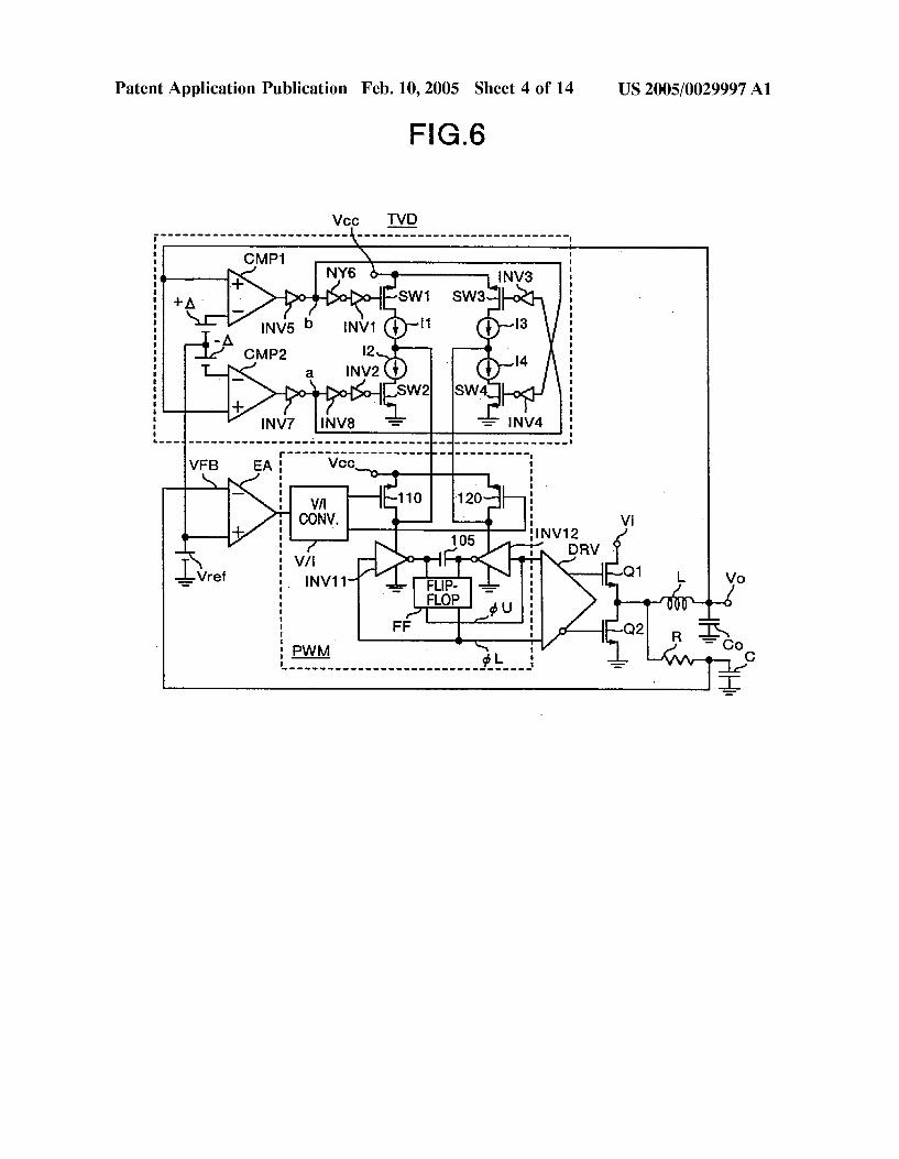
[0050] Embodiment 3
[0051] FIG. 5 illustrates a poWer-supply device obtained by further providing a transient variation detecting circuit TVD into the 1st embodiment. This transient variation detecting circuit TVD controls the duty of the pulse-Width modulation oscillator PWM by detecting a transient load variation betWeen the output voltage Vout at the output terminal V0 and a voltage that results from adding a upper and loWer limit-voltage Width 1A to the reference voltage Vref. FIG. 6 illustrates a concrete example of the pulse Width modulation oscillator PWM and that of the transient variation detecting circuit TVD.
[0052] In FIG. 6, the pulse-Width modulation oscillator PWM is a variable oscillator including a voltage-to-current converting circuit V/I, current-source MOSs 110, 120, inverters INV11, INV12, a capacitor 105, and a ?ip-?op FF. Also, the transient variation detecting circuit TVD includes comparators CMP1, CMP2, sWitching MOSs SW1 to SW4, constant current-sources 11 to 14, and inverters INV1 to INVS.
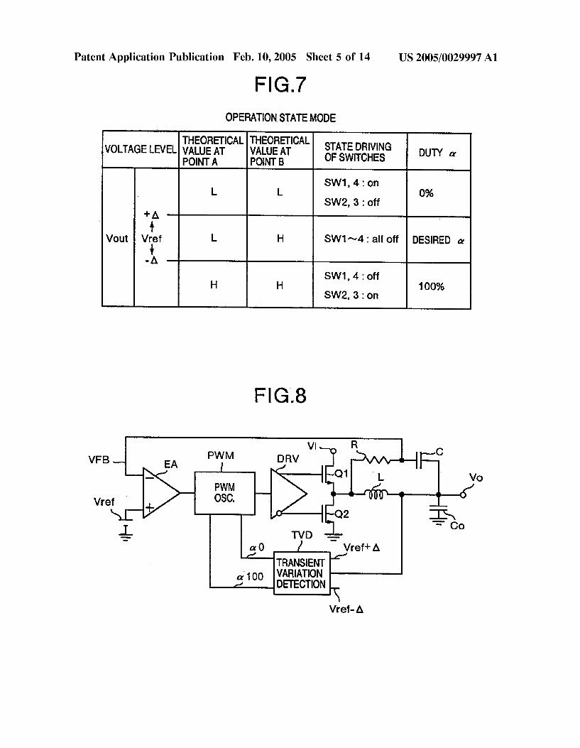
[0053] The transient variation detecting circuit TVD includes a Wind comparator consisting of the 2 comparators CMP1, CMP2. The circuit TVD compares the output voltage Vout With the voltage that results from adding the upper and loWer limit-voltage Width 1A to the reference voltage Vref, thereby detecting the operation state of the output voltage Vout and determining the pulse duty 0t of the oscillator PWM indicated in FIG. 7. This means that, in the transient variation detecting circuit TVD, the control method in the steady state and the one at the transient state are sWitched into control modes that match the operation state.
US 2005/0029997 A1
[0054] From the outputs from the 2 comparators CMP1, CMP2, the following 3-Way information is acquired: (a) a case Where the load current is decreased, (b) the steady state, (c) a case Where the load current is increased. Using FIG. 7, these cases Will be explained beloW:
[0055] The case (a) is under a condition Vout§(Vref+A). At this time, the output duty 0t of the pulse-Width modulation oscillator PWM is forcefully set at 0%. For this purpose, the sWitching MOSs SW1 and SW4 are turned on, and the sWitching MOSs SW3 and SW2 are turned off. As a result, a current from the constant current-source I1 is added to a current from the current-source MOS 110, then ?owing together to the inverter INV1. A current from the constant current-source I4 is subtracted by a current to the current source MOS 120, so that the current value ?oWing to the inverter INV12 becomes equal to 0. Consequently, the upper-side PoWer MOSFET O1 is sWitched off, and the loWer-side PoWer MOSFET Q2 is sWitched on, Which, eventually, makes the duty 0t equal to 0%. In this case, in order to set the duty 0t at 0% completely, it is preferable that current values from the constant current-sources I1 to I4 be each set at the total current of differential pair operation currents of the voltage-to-current converting circuit V/I.
[0056] The case (b) is under a condition (Vref+ A)>Vout>(Vref-A). In this case, all of the sWitching MOSs SW1 to SW4 are turned off, and are operated in accordance With a current ratio determined by a control instruction from the error ampli?er EA. Since this current ratio is equal to the rate of the duty, the voltage that is proportional to the duty 0t of the input voltage Vin can be acquired as the output voltage Vout.
[0057] The case (c) is under a condition Vout§(Vref-A), Where the duty 0t is forcefully set at 100%. In this case, the sWitching MOSs SW3 and SW2 are turned on, and the sWitching MOSs SW1 and SW4 are turned off. As a result, a current from the constant current-source I3 is added to the current from the current-source MOS 120, then ?oWing together to the inverter INV12. A current from the constant current-source I2 is subtracted by the current to the current source MOS 110, so that the current value ?oWing to the inverter INV11 becomes equal to 0. Consequently, the upper-side PoWer MOSFET O1 is sWitched on, and the loWer-side PoWer MOSFET O2 is sWitched off, Which, eventually, makes the duty 0t equal to 100%. In this case, in order to set the duty 0t at 100% completely, it is preferable that the current values from the constant current-sources 11 to 14 be each set at the total current of the differential pair operation currents of the voltage-to-current converting cir cuit V/I.
[0058] The present embodiment forcefully sWitches the duty 0t of the pulse-Width modulation oscillator PWM to either 0% or 100% so that the voltage generated at the output terminal Vo at the transient state Will fall Within the upper and loWer limit-voltage Width 1A added to the reference voltage Vref. This rapidly suppresses the output voltage Vout Within (Vref 1A). Moreover, When the operation state enters the steady state, the present embodiment causes the output voltage to be stabiliZed as the voltage that is proportional to the duty 0t of the input voltage.
[0059] In this Way, in the present embodiment, the control mode is automatically sWitched depending on Whether the operation state is the transient state or the steady state. As a
Feb. 10, 2005
consequence, With respect to even, e.g., an about 10A transient load variation having the high current sleW rate (i.e., di/dt) of 500 A/ys, it becomes possible to simulta neously implement both the high-speed response and the stabiliZation of the output voltage in the steady state.
[0060] Next, using FIG. 20, the description Will be given beloW concerning another embodiment of the pulse-Width modulation oscillator PWM. A circuit illustrated in FIG. 20 can be implemented by a combination of an oscillator OSC, a one-shot multivibrator OSM, and a V/I converter V/I. A constant time-period pulse can be generated by the oscillator OSC as folloWs: A MOS 130 and a constant current-source I5 set a constant current Which is needed for determining the desired time-period. Next, this constant current is made to How to the current-source MOSs 110, 120 of the pulse-Width modulation oscillator PWM in FIG. 6. Also, When this constant time-period pulse is applied to a clock terminal CLK of the one-shot multivibrator OSM, the terminal volt age of a capacitor CT becomes equal to 0 on a temporary basis. At the next moment, hoWever, the capacitor CT is electrically charged by a current that results from converting the error voltage of the error ampli?er EA by the V/I converter V/I. Moreover, a time that has elapsed until this charge voltage attains to a predetermined threshold value is acquired as the PWM pulse. In this Way, the series of pulse-Width modulation oscillating operations can be repeated. Namely, it becomes possible to acquire the PWM pulse that is proportional to the error voltage of the error ampli?er EA.
[0061] This pulse-Width modulation oscillator PWM is used as an effective unit in a multi-phase control in FIG. 11 and FIG. 12 Which Will be described later. In this case, in order to implement the multi-phase operation, a phase shift circuit needs to be inserted after the oscillator OSC.
[0062] Embodiment 4
[0063] FIGS. 8 to 10 illustrate the present embodiment. The embodiment in FIG. 8, Which is obtained by providing the transient variation detecting circuit TVD into the embodiment in FIG. 3, alloWs the acquisition of basically the same effects in FIG. 5. The con?gurations in FIG. 9 and FIG. 10 are as folloWs: In the circuit diagrams in FIG. 1 and FIG. 3, the input into the transient variation detecting circuit TVD is draWn from the midpoint of a series circuit that consists of a capacitor C3 and a resistor R3 Which are set up at both ends of the inductor L of the LC smoothing ?lter. As a result of this, the phase of an inductor L current, Which can be detected by the series circuit of the capacitor C3 and the resistor R3, and the charge/discharge phase of the output capacitor C0 can be made to coincide With each other. Consequently, it becomes possible to eliminate as much as possible excessive/redundant electric charges produced by the charge/discharge of the output capacitor C0 from the inductor L current. This makes it possible not only to implement the high-speed response and the high stability, but also to reduce a variation (i.e., ripple) in the output voltage at the transient state.
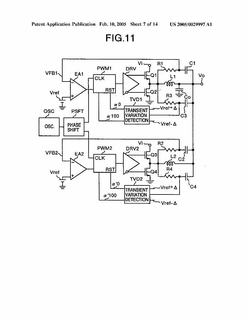
[0064] Embodiment 5
[0065] The present embodiment is a multi-phase embodi ment Where the plural poWer-supply device units in the 1st to the 4th embodiments are operated in parallel. The present embodiment combines the 2 or more same-type poWer
US 2005/0029997 A1
supply devices indicated in the 1st to the 4th embodiments. Hereinafter, the explanation Will be given below selecting the 2-phasing as the example.
[0066] FIG. 11 illustrates the embodiment that results from multi-phasing the poWer-supply device unit in FIG. 8. In order to implement the multi-phasing, the embodiment in FIG. 11 neWly includes the oscillator OSC and a phase shift circuit PSFT, Which generate 2-phase pulses Whose phases are shifted to each other by 180°. This embodiment inputs each of the 2-phase pulses into each of pulse-Width modu lation oscillators PWM1 and PWM2, thereby implementing the multi-phase control.
[0067] FIG. 12 illustrates, in more detail, the embodiment of the poWer-supply device in FIG. 11. In FIG. 12, the pulse-Width modulation oscillator PWM1 includes a volt age-to-current converting circuit V/I1 and a one-shot mul tivibrator OSM1. In the steady state, the oscillator PWM1 operates by receiving a pulse signal from the phase shift circuit PSFT.
[0068] Using an operation state mode in FIG. 13, the explanation Will be given beloW regarding the operation of the embodiment in FIG. 12. This operation state mode Will be explained in much the same Way as the case of the 3rd embodiment. Hereinafter, the explanation Will be given concerning the Phase 1 poWer-supply illustrated on the upper-half side in FIG. 12.
[0069] (a) In the case of Vout§(Vref+A), the output duty of the pulse-Width modulation oscillator PWM1 is forcefully set at 0%. For this purpose, the reset RST of the one-shot multivibrator OSM1 is turned on, Which makes the duty equal to 0%.
[0070] (b) In the case of (Vref+A)>Vout>(Vref-A), as an ordinary operation of the one-shot multivibrator, the OSM1 receives the pulse from the phase shift circuit PSFT as a clock CLK, thereby generating an on-pulse Width. The on-pulse Width is determined by the current value from the current-source MOS 210 and the capacitance value of a capacitor CT1, i.e., a timing capacitor. This on-pulse Width is of a control mode that operates in accordance With the current ratio determined by the control from the error ampli?er EA. Namely, since this current ratio is equal to the duty, the output voltage Vout becomes equal to the voltage that is proportional to the duty 0t of the input voltage Vin.
[0071] (c) In the case of Vout§(Vref-A), the duty is forcefully set at 100%. For this purpose, both ends of the capacitor CT1, i.e., the timing capacitor, are short-circuited by a MOS sWitch M21 so as to maintain the on-state, Which makes the duty equal to 100%. Incidentally, a detection result by an overcurrent detecting circuit OC1 is also added to the reset RST, thereby preventing a component break doWn caused by an overcurrent from the upper-side PoWer MOSFET Q1. Concerning the Phase 2 poWer-supply on the loWer-half side in FIG. 12, the explanation Will be omitted because the operation is the same as the Phase 1 poWer supply.
[0072] In the operations described so far, in the steady state, the inductor currents from the 2 poWer-sources operate in opposite phases, i.e., in phases shifted to each other by 180°. MeanWhile, at the transient time, the inductor currents from the 2 poWer-supplies become the same in their phases, thereby dealing With a rapid load variation. The present
Feb. 10, 2005
embodiment not only increases the output current by using the plural poWer-supplies, but also reduces a ripple in the output voltage.
[0073] In the case of providing the 2 or more poWer supply device units, there are provided an oscillator and a phase shift circuit that the plural poWer-supply device units have in common. Moreover, in the steady state, phases of driving pulses of the upper-side/loWer-side PoWer MOS FETs in the respective poWer-supply device units are respec tively shifted to phases that result from dividing 360° by the number of the poWer-supply device units located in parallel. At the transient state, as are the cases With the above described (a) and (c), all of the parallel poWer-supply device units are operated by driving pulses of one and the same phase. In the case of, e.g., the 4 poWer-supply device units, it is advisable to shift the phases to the respective phases of 0° (i.e., criterion), 90°, 180°, and 270°.
[0074] Embodiment 6
[0075] Next, the explanation Will be given beloW concern ing an embodiment of the IC chip con?guration of the poWer-supply control device in the present invention.
[0076] FIG. 14 illustrates the embodiment of the one-chip con?guration of the circuit con?guration illustrated in FIG. 8. In FIG. 14, circuits and functions are all implemented on-chip on one semiconductor board except for the folloW ing externally-mounted components: The LC smoothing ?lter, the CR circuit consisting of the capacitor C3 and the resistor R3 for detecting the current phase of the transient variation detecting circuit TVD, and a boost circuit consist ing of a diode DBT and a capacitor CBT.
[0077] The on-chip implemented circuits and functions are as folloWs: The CR smoothing ?lter consisting of the capacitor C and the resistor R, the error ampli?er EA, the reference voltage Vref, the pulse-Width modulation oscilla tor PWM, a dead band circuit DBU, a dead band circuit DBL, a level shift circuit LS, a driver DRVU, a driver DRVL, the upper-side/loWer-side PoWer MOSFETs Q1, Q2, an overcurrent detecting circuit OC, the transient variation detecting circuit TVD, an upper and loWer limit-voltage generating circuit VA, a soft-start circuit SS, an under voltage lockout circuit UVLO, and a poWer-good circuit PWRGD. Incidentally, instead of acquiring the reference voltage Vref from a band-gap reference circuit, the reference voltage Vref may be acquired by receiving a digital signal corresponding to a VID (: Voltage Identi?cation) code, using an on-chip D/A converter illustrated in FIG. 15. Although there exist not-illustrated circuits and functions, the 1-chip poWer-supply control IC in the present embodiment is equipped With the functions implemented in compliance With the VRM 9.1 expounded by the Intel Corporation.
[0078] Although, in FIG. 14, the explanation has been given selecting the case Where the upper-side PoWer MOS FET Q1 is the NMOS, the MOSFET Q1 may also be a PMOS. In this case, the externally-mounted boost circuit becomes unnecessary. HoWever, since it is necessary to drive the gate of the PMOS at the electric potential from the input terminal Vi, a voltage-generating supply for this neces sity is implemented on-chip.
[0079] The voltage fed to the input terminal Vi and the one fed to a poWer-supply terminal Vcc may be made equal to each other, e.g., 5V or 12V. OtherWise, the voltages may be