Power Stability Enhancement and Performance...
16
Power Stability Enhancement and Performance Analysis of 48-Pulse Three Level STATCOM Using FinFET Technology 1 S.K. Rajesh, 2 S. Poorani, 3 John Chembukkavu and 4 K.N. Chandra Bose 1,2,3,4 Department of EEE, Karpagam University, Karpagam Academy of Higher Education, Coimbatore, Tamil Nadu, India. Abstract This research initiates a new approach for power quality enhancement that regards as an advanced STATCOM 48-pulse with FinFET technology. Cascaded Static Synchronous Compensator (STATCOM) provides effectual solution for reactive power support voltage in middle/high circumstances, and it is extensively engaged to manage reactive power. A novel phase current reference evaluation technique is anticipated to hold up reactive power recurrently underneath unusual voltage circumstances in view of voltage balancing control and phase current constraint. Limitations among voltage and current phasors of STATCOM are realized .Mounting power densities in current technologies has determined significance in enhancing energy efficiency in the course of near-threshold operation. The work investigates the impact of device characteristics, for instance drain-induced barrier lowering and sub-threshold slope, on near-threshold competence and performance. FinFET’s enhanced channel characteristics more than double energy efficiency gains contrast to current planar nodes also FinFET facilitates gate control on multiple sides of the fin, which progresses electrostatic control. The projected idea permits the recompense the reactive power by absorbing/producing a current flow correspondent to the essential reactive power better than the existing IEEE HVDC 30-Bus System. The recital of the anticipated model is simulated in MATLAB environment. Key Words:FinFET, STATCOM, phase current, reactive power, electrostatic control. International Journal of Pure and Applied Mathematics Volume 116 No. 21 2017, 693-708 ISSN: 1311-8080 (printed version); ISSN: 1314-3395 (on-line version) url: http://www.ijpam.eu Special Issue ijpam.eu 693
Transcript of Power Stability Enhancement and Performance...

Power Stability Enhancement and
Performance Analysis of 48-Pulse Three
Level STATCOM Using FinFET Technology 1S.K. Rajesh,
2S. Poorani,
3John Chembukkavu and
4K.N. Chandra Bose
1,2,3,4 Department of EEE, Karpagam University,
Karpagam Academy of Higher Education,
Coimbatore, Tamil Nadu, India.
Abstract This research initiates a new approach for power quality enhancement
that regards as an advanced STATCOM 48-pulse with FinFET technology.
Cascaded Static Synchronous Compensator (STATCOM) provides effectual
solution for reactive power support voltage in middle/high circumstances,
and it is extensively engaged to manage reactive power. A novel phase
current reference evaluation technique is anticipated to hold up reactive
power recurrently underneath unusual voltage circumstances in view of
voltage balancing control and phase current constraint. Limitations among
voltage and current phasors of STATCOM are realized .Mounting power
densities in current technologies has determined significance in enhancing
energy efficiency in the course of near-threshold operation. The work
investigates the impact of device characteristics, for instance drain-induced
barrier lowering and sub-threshold slope, on near-threshold competence
and performance. FinFET’s enhanced channel characteristics more than
double energy efficiency gains contrast to current planar nodes also FinFET
facilitates gate control on multiple sides of the fin, which progresses
electrostatic control. The projected idea permits the recompense the
reactive power by absorbing/producing a current flow correspondent to the
essential reactive power better than the existing IEEE HVDC 30-Bus
System. The recital of the anticipated model is simulated in MATLAB
environment.
Key Words:FinFET, STATCOM, phase current, reactive power,
electrostatic control.
International Journal of Pure and Applied MathematicsVolume 116 No. 21 2017, 693-708ISSN: 1311-8080 (printed version); ISSN: 1314-3395 (on-line version)url: http://www.ijpam.euSpecial Issue ijpam.eu
693

1. Introduction
Transmission methods show continuous changes in hasty reconstruction across
worldwide. The operating mode is initiated newly with the profound load is
under consideration. As well, most loads are unbalanced or non-linear. Higher
amount of quality problem is encountered in the power systems consequently
such as harmonics current burden, extreme neutral current, high reactive power
poor voltage regulation etc. Numerous methods and procedures are
accomplished to suppress the power quality problem across the country.
STATCOM technology [1] has been highly utilized for its faultless and flexible
performance, yet still under investigation and development. STATCOM is
competent to counter measure grid errors and asymmetrical voltages in several
three-phase grid connected scheme. There are huge literature relating to the
conventional two-level STATCOM along with general dc-link. The reactive
power control technique and the processing principle are examined thoroughly.
STATCOM should provide reactive power [2] incessantly under asymmetrical
grid, in the recent investigations. To improve its fault ride-through potential and
to reduce the torque oscillations [3], a coordinated control of the positive and
negative sequence reactive power was hold up by the induction generator. To
deviate the positive sequence voltage and to negative sequence voltage, a
collaborated reactive power control is introduced. Safe current injection policies
for STATCOM are proposed to sustain reactive power and to promise the
enduring injected current within the protection operating limit. Here high
quality power production and huge security is offered. A novel reactive power
controller of a STATCOM has been proposed and examined along with its
performance. Certain significant factors are associated with the static
synchronous compensator (STATCOM) in the existing works.
The Static Synchronous Compensator (STATCOM) is capable of absorbing/
producing the outcome to manage the electrical power system, which is also
known as shunt associated reactive compensation equipment. The operating
characteristics associated with the rotating synchronous compensator, is offered
by the STATCOM to evaluate mechanical inertia. solid state power switching
devices are utilized by the STATCOM to obtain the quick controllability of
three phase voltages, mutually in phase angle and magnitude as shown in Fig 1.
The DC side of the STATCOM comprises of DC source or energy storage
device, thus offering an active power to the power system. This helps in
accomplishing the regulation of the phase angle of AC power system and the
phase angle of STATCOM terminals. The STATCOM suppresses the active
power of the AC system when the phase angle of the AC power system is
directed by the VSI phase angle. The real power of the STATCOM is obtained
when the phase angle of AC system holds the VSI phase angle.
Fig. 1: Schematic of Static Synchronous Compensator
International Journal of Pure and Applied Mathematics Special Issue
694
2. Control Technology
The control signal of outer loop regulator measures the reference value of
voltage, current or reactive power of the STATCOM device using the
measurement obtained by the compensator. Three essential structures termed
closed-loop control, open-loop control, and combination of open-loop control
and closed-loop control, is determined based on the functionality and necessity
of the control approach. With reference to the control technology, STATCOM
control includes differential geometric control, nonlinear robust control,
adaptive recurrent neural network control, fuzzy control, the inverse system PI
control, and so on. Owing to the physical quantities, a control technique
provides indirect current control and direct current control by altering the
reactive current reference value produced by the STATCOM reactive current.
Direct Current Control
Direct current control and PWM control is utilized for evaluating the direct
value of current waveform in a feedback control. In the control strategy , the
reactive module of instantaneous current has higher reference value, as well the
reference value of reactive current obtain the voltage sine wave by increasing
the reactive current reference. To obtain the complete instantaneous current
reference value Iref STATCOM supports the active power to acquire the
correction of phase IQref. The control technology utilizes triangular wave and
hence compared with the existing control techniques. The semiconductor
switching devices have higher switching frequency, necessitating power to
control current instantaneous value. This technique is restricted completely, in
case of high power STATCOM whereas medium and small capacity
STATCOM is highly desirable.
Indirect Current Control
To control the STATCOM AC current indirectly, indirect current control [4] is
offered by STATCOM AC voltage inverter with respect to the amplitude and
phase of the elementary device. The p-q decomposition find outs the
active/reactive power of STATCOM absorbed, The active power and the
reactive power of STATCOM is soak up by the feedback control. The outcome
of the DC voltage regulator is utilized to evaluate the active current reference
value. The absorbed active/reactive power of STATCOM is identified; also the
outcome of the indirect current control technique of STATCOM has huge
capacity. Higher amount of harmonics [5] is generated by the output voltage, in
the capacity scheme. The DC voltage exploitation is reduced as the switching
frequency is reduced. To reduce the harmonics multi-level control is utilized.
48 Pulse 3 Level STATCOM with Filter Design
The 48-pulse digital STATCOM power system shows absolutely new
performance and is examined in this experimentation. The simulation of the
digital technique is carried out by means of the MATLAN environment. The
preliminary building block for a STATCOM is 48-pulse converter cascade [6]
International Journal of Pure and Applied Mathematics Special Issue
695

as revealed in Fig 2. A novel decoupled current control approach shows control
procedure mutually in both direct and quadrature current components of
STATCOM. With the use of capacitive and inductive modes full STATCOM
performance is completely investigated in a load excursion and power
transmission system. Compared to the low-order or functional models the
exploitation of full 48– pulse STATCOM is highly desirable.
Fig. 2: 48 Pulse 3 Level FinFET Topology
A supplementary regulator loop along with dc capacitor voltage is used to
enhance the dynamic performance of the full 48-pulse STATCOM device as
represented in [7]. The variation rate of the dc voltage is chosen to charge the dc
side capacitor voltage. An unchanging short time interval is chosen
consequently, to deliberate the variation of Vdc magnitude, also the
transformation of the dc voltage is calculated quickly. When this alteration is
enhanced than the significant threshold, the supplementary loop has been
triggered. The speedy variation of dc capacitor voltage is sensed and this is a
predominant idea. The supplementary damping regulator is highly accurate for
the phase angle of STATCOM device voltage with respect to the
positive/negative sign of variation. The dc capacitor is charged extremely fast.
The STATCOM converter voltage lacks the ac system voltage in return. To
recompense several internal losses and to maintain the voltage of the capacitor
at preferred level, a small amount of active power is soak up by the converter.
To increase/decrease the capacitor voltage, the similar technique is utilized.
Thus, the converter output voltage amplitude is controlled based on Var
production/absorption. The content of the supplementary loop decreases while
charging /discharging the capacitor. The ripple content shows progress in the
controllability of STATCOM.This ripple contented in and progresses rapid
Fig. 3: 48 Pulse 3 Level FinFet Topology With Filter
The performance of the STATCOM is essential with the leakage reactance Xt of
a step-down transformer, a dc side voltage and a three-phase VSI. The reactive
power is exchanged based on the transformer leakage reactance with dissimilar
International Journal of Pure and Applied Mathematics Special Issue
696

ac voltage amongst the STATCOM device and the power system juncture. To
enhance the voltage profile the interconnected power system, the voltage can be
synchronized, as well significant duty of the STATCOM as displayed in the Fig
3. The dynamic power system of the STATCOM is improved by means of
secondary damping function [8][9].
The principle function of the STATCOM is to control the magnitude of bus
voltage by producing/absorbing the reactive power of ac grid network similar to
that of thyristor static compensator. With response to the leakage reactance of
coupling transformer along with secondary transform r voltage and with
primary voltage (network side), the reactive power transfer is examined.
48 Pulse 3 Level STATCOM without Filter Design
The Static Synchronous Compensator (STATCOM) is based on power
electronics devices, is a shunt device to manage voltage to compensate reactive
power [10], and progress transient stability. Figure 4illustrates the fundamental
method of a STATCOM connected to a bus of the transmission system. The
outcomes of applying a STATCOM are alike of a rotating synchronous
condenser [11], but devoid of its mechanical inertia and slow time response.
Fig. 4: 48 Pulse 3 Level FinFET Topology
The STATCOM primarily consists of a three-phase voltage source converter
(VSC), DC capacitor and a step-down transformer with leakage reactance. The
total reactive power is calculated based on the power absorbed from the power
system, in which the magnitudes of the terminals are controlled by the
STATCOM. STATCOM generates reactive power (STATCOM capacitive)
when the system voltage is low. In contrast, when the voltage is high, the
reactive power soaks up (STATCOM inductive) capacitor, C which stimulates
the AC line. The bus voltage dynamic regulation and dc link voltage is
guaranteed by utilizing the decoupled control [12]. The two components of the
STATCOM current are named as quadrature axis component, Iq and direct axis
component, Id with reference to line voltage, dealt with the use of PLL. Iq is
contrast with the reference current (Iqref) attain from the outer regulation loop
for ac-voltage regulation, utilized to direct the reactive power as illustrated in
Fig.5.
International Journal of Pure and Applied Mathematics Special Issue
697

Fig. 5: 48 Pulse 3Level FinFET Topology without Filter
3. Overview of FinFET Technology
Fin-type field effect transistors (FinFET) [13] [14] are capable alternate for bulk
MOS at the nano scale. This is since the fabrication technology of FinFET is
approximately the similar as that of the conventional MOS transistor. Owing to
the detail, fabrication process is alike, FinFETs can effortlessly substitute
MOSFETs in the near outlook. FinFETs are the double gate (DG) transistors
family and are essentially quasi-planar in environment. They are expressed as
quasi-planar since of the fact that the current direction is equivalent to its wafer
and the channel is formed perpendicular to it. FinFETs gate terminal can either
be shorted or separately controlled to bid rich design space. Thin silicon body
and the two electrically coupled gates of the FinFET are recognized very well
from literature to restrain the short channel effects.
A SOI substrate constructs a double gate transistor based on the DELTA (single
gate) transistor design. The characteristics of FinFET is shown that a thin
silicon “fin” constructs a channel, that is wrapped by the device body. Over
32nm technology, there is important decrease in Average power utilization
when FinFET is cast off as a substitute of MOSFET.
The FinFET device structure comprises of a silicon fin enclosed by shorted or
independent gate on either side of the fin, characteristically on silicon insulator
substrate. FinFET has two gates, which can be functional independently or tied
mutually. The threshold voltage at one gate can be proscribed with the
assistance of voltage at the other gate. In the short channel effects, single-gate
mode, (roll-off threshold voltage, sub threshold swing humiliation and drain
induced barrier lowering) are in reality less harsh than those of the device in the
double-gate mode.
Challenges in FinFET
Despite of guarantying higher performance and improved power stability, the
FinFET technology projects a novel challenge: Primarily, overcoming the
FinFET width, the significant challenge is the discrete size of Fin. The I-V
characteristics of the FinFET device show the impact on changeable width, and
also they are examined. It is experimental that the fin width is reduced, the
predominate drain current is concentrated at lower gate voltage magnitude. The
International Journal of Pure and Applied Mathematics Special Issue
698

actuality of the device is predictable with lower fin width which reduces the
short channel effect by sinking the fin width. Amplified source/drain (S/D)
resistance tends to reduce the drive current and trans-conductance of the device.
The performance of the device based on the on off I / I proportion relates to the
wide ranging fin width. When the fin width is greater, the on off I / I reduced
significantly and also experimented. In case of FinFET technology, the
characteristics of this technology is improved based on the width of the Fin.
The sub-threshold slope is greater, when the width of the fin enlarges. This
observation shows that the performance of the FinFET is higher when the width
of the Fin is reduced. When the fin width declines the performance, the parasitic
drain/source resistance is enhanced to reduce the drive current. Also, the device
temperature is higher, when the heat unable to flow effortlessly with respect to
the slighter increase of Fin width. This effect is more effectual in SOI
technology. The self-heating effect appropriate to low thermal conductivity of
oxide layer, the insulating layer is buried. Corner effect is termed, that the two
corner area of the neighboring gates shares the charge based proximity of tri
gate FinFET. Thus, the premature inversion is increased and sensed at the
corners. Fin corners shows rigorous gate-to-channel electric field at the corners.
These consequences the gate-to-source input voltage that enhanced toward the
device threshold, there will shows greater concentration of sub threshold
leakage current at the corners of fin, which is recognized as “corner effect”.
This corners of the triple gate FinFET humiliates the sub-threshold
characteristics during premature inversion of FinFET which exhibits superior
off state leakage current.
4. Simulation Results
Now, after the execution of the STATCOM comprising 48-Pulse three-level
converter [15], as well fig 6. shows the STATCOM current and voltage
distribution at load terminal. The capacitors in the STATCOM acts like a
variable DC voltage source. At this point, the capacitors modeled and pretend
are charged originally (initial conditions) by system voltage. The amplitude
voltage (variable) generated is synthesized from variable DC voltage by the
inverter.
When the motor starts functioning at “t” sec, the rms voltage dip is initiated as
well. As shown in Fig 6. A slight voltage dip is observed in the implementation
of STATCOM. The current lags about an angle of 90° from the system voltage
i.e. reactive power is supplied by the STATCOM system throughout the voltage
sag.
The FFT examination of STATCOM‟s output obviously illustrates the 48-
pulses cycle of yield voltage contains a lesser harmonics (THD = 30.91%) as
shown in Fig.7 below. It is also seen that harmonics are offered in the voltage as
predictable. Approximately, 25% of voltage dip is examined in the system
voltage, whenever the inductance motor is in progress. As shown in fig. 8, when
the motor starts working on “t” seconds for about 4-5 cycles, the voltage-dip is
International Journal of Pure and Applied Mathematics Special Issue
699
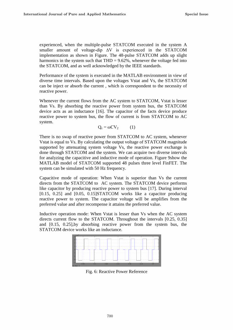
experienced, when the multiple-pulse STATCOM executed in the system A
smaller amount of voltage-dip ∆V is experienced in the STATCOM
implementation as shown in Figure. The 48-pulse STATCOM adds up slight
harmonics in the system such that THD = 9.62%, whenever the voltage fed into
the STATCOM, and as well acknowledged by the IEEE standards.
Performance of the system is executed in the MATLAB environment in view of
diverse time intervals. Based upon the voltages Vstat and Vs, the STATCOM
can be inject or absorb the current , which is correspondent to the necessity of
reactive power.
Whenever the current flows from the AC system to STATCOM, Vstat is lesser
than Vs. By absorbing the reactive power from system bus, the STATCOM
device acts as an inductance [16]. The capacitor of the facts device produce
reactive power to system bus, the flow of current is from STATCOM to AC
system.
Qc = ωCV2 (1)
There is no swap of reactive power from STATCOM to AC system, whenever
Vstat is equal to Vs. By calculating the output voltage of STATCOM magnitude
supported by attenuating system voltage Vs, the reactive power exchange is
done through STATCOM and the system. We can acquire two diverse intervals
for analyzing the capacitive and inductive mode of operation. Figure 9show the
MATLAB model of STATCOM supported 48 pulses three level FinFET. The
system can be simulated with 50 Hz frequency.
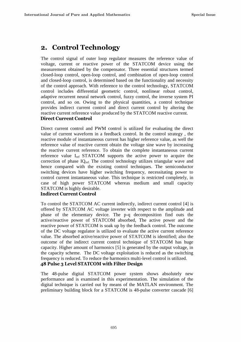
Capacitive mode of operation: When Vstat is superior than Vs the current
directs from the STATCOM to AC system. The STATCOM device performs
like capacitor by producing reactive power to system bus [17]. During interval
[0.15, 0.25] and [0.05, 0.15]STATCOM works like a capacitor producing
reactive power to system. The capacitor voltage will be amplifies from the
preferred value and after recompense it attains the preferred value.
Inductive operation mode: When Vstat is lesser than Vs when the AC system
directs current flow to the STATCOM. Throughout the intervals [0.25, 0.35]
and [0.15, 0.25],by absorbing reactive power from the system bus, the
STATCOM device works like an inductance.
Fig. 6: Reactive Power Reference
International Journal of Pure and Applied Mathematics Special Issue
700
Fig. 7: FFT Analysis of STATCOM Without Filter
Fig. 8: Waveform of Voltages in All Bus System with STATCOM in Transmission System
Fig. 9: FFT Analysis of STATCOM Without Filter
5. Influence of FinFET Technology
Over STATCOM
In this segment, leakage power examination of FinFET grounded on inverter
and CMOS based inverter is done. Leakage power is the power devoted when
the device is in off state. Leakage power decrease is very critical in sub-
threshold circuits. In order to compute leakage power of inverter, the input and
output of the inverter are associated to two stage buffers. This set up was called
as inverter chain. The circuit under test (CUT) is measured for the leakage
power examination. As the inverter is the nucleus of all digital plans and the
electrical performance of digital circuits can be approximately completely
resultant by concluding the outcomes attained for inverter circuit, this effort
have taken inverter as a bench marking circuit for the investigation. Leakage
Power is mathematically articulated as IOFFVDDLeakage Power, Where IOFF is
leakage current and VDD is supply voltage of the circuit.
VD is the drain voltage and VS is the source terminals voltage, respectively, and
φ the potential distribution fully depleted inside Si fin [18], with adequate
boundary conditions the equation can be solved. Leakage current is attained
when drain voltage is zero. IOFF = IDS at VD=0 In this paper, supply voltage is
varied from 0.1 V to 0.45 V and leakage power of mutually CMOS grounded
inverter and FinFET based inverter (circuit under test) are renowned. Variability
examination of both is also executed.
International Journal of Pure and Applied Mathematics Special Issue
701

Variability is distinct as the proportion of standard deviation to mean (σ/µ) of a
design metric. It is experimental that FinFET supported inverter is less variable
evaluated to that of CMOS based inverter. The leakage power in FinFET based
inverter is extremely less contrast to that of CMOS based inverter. As the device
shrinks, leakage increases. But it is set up that a FinFET based circuit, at 32 nm
technology node, with oxide thickness 0.9 nm, silicon film thickness „X‟ nm,
dielectric constant and channel doping concentration acquires lower leakage
power as contrast to that of CMOS based circuit [19]. This work believes lightly
doped channel region to stay away from humiliating of carrier mobility and
threshold voltage variations. Short channel effects are also abridged. This makes
the FinFET supported circuit applicable for ultralow power operation [20]. It is
experimental that there is an enhancement in mean value of leakage power (its
variability). It is imperative that power dissipation of FinFET[21]supported
inverter is approximately invariant, while power dissipation of CMOS based
inverter diverges with supply voltage variation. This entails that FinFET based
devices and circuits are appropriate for ultralow power applications similar to
moveable and wearable devices. In this manuscript, other design metrics like
propagation delay (delay), energy delay product (EDP) and power delay product
(PDP)at supply voltage are not observed [22].
It is experimental that FinFET based inverter displays desirable outcome in
terms of delay, energy delay and power-delay product of product as contrast to
those of CMOS based inverter. FinFET grounded inverter attains enhancement
in propagation delay. It means that FinFET based inverter is quicker contrast to
CMOS based one.
The off-state current is amplified as a result of tunneling effect and carrier
mobility, when the body doping absorption is enlarged by the Short channel
effects of bulk MOSFET. High halo doping is chosen to have a control over this
effect as a result, it degrades the current and amplifies tunneling. By adapting
the minimum device structures [23], the scaling benefits are exploited. The level
of integration is obtained as a result of FinFET technology. FinFET is
constructed on the SOI substrate by making a non-planar and double gate to
develop a Depleted Lean-channel Transistor design. The significant
characteristics of FinFET are made self-determined and biased by the front and
back gates, and also biased to control the threshold voltage and the current. To
solve the scaling obstacles, Double gate FinFET technology is implemented.
The working of FinFET is provided in four different modes, initially tied-gate
(SG) mode, Independent Gate (IG) mode, LP/IG mode and Low Power (LP)
mode. The gate sides are separately restrained in the IG mode FinFET.
Independent gate biasing due to multi-threshold voltage is reduced by the
number of transistors. The cell stability and performance is enhanced with the
minimization of leakage. With the minimized size of transistors, the read cycle
is functionally suitable for direct-data method. Thus, the IG-FinFET shown in
Table I reveal better stability in SRAM cell.
International Journal of Pure and Applied Mathematics Special Issue
702
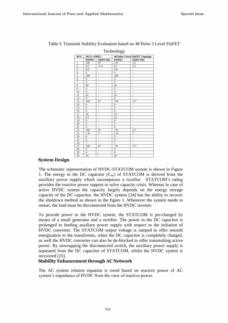
Table I: Transient Stability Evaluation based on 48 Pulse 3 Level FinFET
Technology BUS SFCL+SMES 48 Pulse 3 level FinFET Topology
P(MW) Q(MVAR) P(MW) Q(MVAR)
1 168 67 176 117
2 8.5 11.4 8.7 3.3
3 4.8 - 4.8 -
4 0 - 0 -
5 188 - 188 -
6 0 - 0 -
7 0 - 0 -
8 60 - 60 -
9 0 - 0 -
10 0 - 0 -
11 22 - 22 -
12 0 - 0 -
13 168 67 176 117
14 0 - 0 -
15 0 - 0 -
16 0 - 0 -
17 18 - 18 -
18 6.2 - 6.2 -
19 0 - 0 -
20 0 - 0 -
21 0 - 0 -
22 168 67 176 117
23 1.41 2 1.41 2
24 0 - 0 -
25 0 - 0 -
26 7 - 7 -
27 168 67 176 117
28 0 - 0 -
29 0 - 0 -
30 20 - 20 -
System Design
The schematic representation of HVDC-STATCOM system is shown in Figure
1. The energy to the DC capacitor (Cdc) of STATCOM is derived from the
auxiliary power supply which encompasses a rectifier. STATCOM‟s rating
provides the reactive power support to solve capacity crisis. Whereas in case of
active HVDC system the capacity largely depends on the energy storage
capacity of the DC capacitor. the HVDC system [24] has the ability to recover
the shutdown method as shown in the figure 1. Whenever the system needs to
restart, the load must be disconnected from the HVDC inverter.
To provide power to the HVDC system, the STATCOM is pre-charged by
means of a small generator and a rectifier. The power in the DC capacitor is
prolonged to feeding auxiliary power supply with respect to the initiation of
HVDC converter. The STATCOM output voltage is ramped to offer smooth
energization to the transformer, when the DC capacitor is completely charged,
as well the HVDC converter can also be de-blocked to offer transmitting active
power. By unwrapping the disconnected switch, the auxiliary power supply is
separated from the DC capacitor of STATCOM, whilst the HVDC system is
recovered [25].
Stability Enhancement through AC Network
The AC system relation equation is owed based on reactive power of AC
system‟s impedance of HVDC from the view of reactive power.
International Journal of Pure and Applied Mathematics Special Issue
703

Consumption of Reactive Power in HVDC
The need of AC reactive power can be satisfied by the reactive power directed
by the filter or capacitor. It can sufficiently supplied or absorb the variations of
AC system‟s reactive power. Thus, the bound of the STATCOM is organized by
enlarging the Maximum Available Power (MAP) of HVDC [26]. The voltage
stability and MAP capability is affected by the STATCOM capacity [27].
If the STATCOM is not located towards the HVDC station, but located near the
AC system, MAP is enlarged. Based on the position of the STATCOM, the
variation is associated with the AC impedance angle.
Qs + QHVDC - Qf - QSC = 0 (2)
QSC - STATCOM
Qf – Filter or capacitor reactive power
QHVDC - consumed Reactive Power by HVDC
Qs - Reactive power due to AC system impedance
Table II: Evaluation of HVAC and HVDC based on 48 Pulse 3 Level FinFET Topology
BUS SFCL+SMES
(kV) 48 Pulse 3 level FinFET Topology
HVAC HVDC HVAC HVDC
1 46 - 46 -
2 38 - 46 -
3 - 46 - 46
4 - 46 - 46
5 - 46 - 46
6 - 46 - 46
7 - 46 - 46
8 - 46 - 46
9 - 46 - 46
10 - 46 - 46
11 - 46 - 46
12 - 46 - 46
13 46 - 46 -
14 - 46 - 46
15 - 46 - 46
16 - 46 - 46
17 - 46 - 46
18 - 46 - 46
19 - 46 - 46
20 - 46 - 46
21 - 46 - 46
22 46 - 46 -
23 30 - 30 -
24 - 46 - 46
25 - 46 - 46
26 - 46 - 46
27 46 - 46 -
28 - 46 - 46
29 - 46 - 46
30 - 46 - 46
The result demonstrates the specific fault condition, „Fault current‟ whenever
the HVAC transmission system is added greater than that of the HVDC
transmission system as depicted in the Table II. The occurrence of HVAC
transmission system [28] fault current is highly destructive when the effects are
negligible, moderate and cause less damage in HVDC transmission system.
HVDC does not have the stability crisis since of the absence of frequency, and
International Journal of Pure and Applied Mathematics Special Issue
704
thus, no distance restriction.
The STATCOM or SSC capable for producing or absorbing reactive power that
yields specific factors foe electric power system. This is also specified as a
shunt-connected reactive-power compensation device. a solid-state switching
converter is proficient to produce or absorb the active and reactive power of the
controller to the output terminals, when the energy storage device or the energy
source acts as an input terminal [29]. The required commutation voltage is
provided by the STATCOM to the HVDC system, in which the recompensation
of reactive power to the network is done through steady-state circumstance, as
well throughout the transient circumstance under dynamic condition. During the
transient condition, STATCOM provides limited active power support to the
network. To manage the harmonic necessity [30], the STATCOM supplies
active filtering at low-order harmonics. Furthermore, the capacitor banks are
utilized to compensate the reactive power load cycle variation and also places
anywhere in the network.
6. Conclusion
In this segment, we have examined voltage and current outline for diverse cases
in HVDC line with and without STATCOM filters. This effort also considered
the outcome of power swing on transmission line components like transformers
etc. with MATLAB. This paper illustrates about the widespread of this project
which has sign up all aspects for High voltage direct current (HVDC)
transmission. High-quality HVDC design begins with a comprehensive
understanding of the essential ideas, and operation and control of HVDC
method. There are many bases for operation and control before acting on them,
but for High voltage direct current (HVDC) transmission there are numerous
restrictions. Therefore it is essential to test the systems for diverse condition,
and inspecting the system for bounded violations by means of characteristics of
Power Flow. This paper demonstrates the fault current examination and the
contrast among the HVAC and HVDC power transmission system with better
stability compared to the existing methods along with the FinFET Technology.
The work can further extended by calculating the power stability using Unified
power quality conditioner(UPQC) with NN and PI.
References [1] Bayliss T., Elgarrista F., Thompson S., Yedla R., Perrier J., Arani S., Dyke K.,
Development of a modular cooling solution for STATCOM and HVDC transmission schemes’ IEEE Transaction on Power systems.
[2] Tiefu Zhao, Subhashish Bhattacharya, Alex Q. Huang, Operation of Series and Shunt Converters with 48-pulse Series Connected Three-level NPC Converter for UPFC, IEEE Transactions on Power Systems (2008).
[3] Saha R., Singh B., Improved 48-pulse static synchronous compensator for high-voltage applications, IET Power Electronics (2009).
International Journal of Pure and Applied Mathematics Special Issue
705

[4] Ying Z., Bo-wen S., Research on STATCOM Principle and Control Technology, IEEE transactions of Power Electronics (2011).
[5] Tusharkumar S.J., Geholt D.M., Tandel M.M., Sathvara M.J., 48 Pulse STATCOM for Improving voltage profile and harmonic reduction based on PI controller, International Journal for Scientific Research and Development 2(2014), 791-795.
[6] Litty Joseph, Neetha John, Smitha Paulose, VAR Compensation and Power Quality Improvement by 48-Pulses Three Level STATCOM, International Journal of Advanced Research in Electrical, Electronics and Instrumentation Engineering 5(8) (2016).
[7] Aali S.R., Nazarpour D., 48-Pulse GTO Interline Unified Power Flow Controller, 1st IEEE Power Electronic & Drive Systems & Technologies Conference (2010).
[8] Salemnia A., Khederzadeh M., Ghorbani A., Mitigation of Subsynchronous Oscillations by 48-Pulse VSC STATCOM Using Remote Signal, IEEE Power Tech Conference (2009).
[9] Bhim Singh, Saha R., Enhancing Power Transfer Capacity of Transmission System by a Reduced Magnetics Based 48-Pulse STATCOM Controller, Joint International Conference on Power System Technology and IEEE Power India Conference (2008).
[10] Ravi Balam, Kotyada Kalyani, Shankar Prasad B., Dynamic Performance of 48-pulse STATCOM, SSSC and UPFC controller, International Journal of Engineering Research and Applications 2(1) (2012), 156-163.
[11] Bandopadhyay S., Roy A., Digital Simulation of 48 Pulse GTO Based Statcom and Reactive Power Compensation, International Journal on Recent and Innovation Trends in Computing and Communication (2014), 824-827.
[12] Bhim Singh, Kadagala Venkata Srinivas, Fuzzy Logic Control with Constant DC Link Voltage of 48-Pulse VSC Based STATCOM, IEEE Transactions on Power Electronics.
[13] Brad D. Gaynor, Soha Hassoun, Fin Shape Impact on FinFET Leakage With Application to Multithreshold and Ultralow-Leakage FinFET Design, IEEE Transactions On Electron Devices (2014).
[14] Nebojsa Jankovic, Olga Kryvchenkova, Steve Batcup, High Sensitivity Dual-Gate Four-Terminal Magnetic Sensor Compatible With SOI FinFET Technology, IEEE Electron Device Letters 38(6) (2017).
[15] Abderrahmen Abdellaoui, Abderrazak Yangui, Amara Saidi, Hsan Hadj Abdallah, STATCOM-Based 48-Pulses Three Level GTO Dedicated to VAR Compensation and Power Quality Improvement, International Conference on Sustainable Mobility Applications, Renewables and Technology (2015).
[16] Ashwin Kumar Sahoo, Murugesan K., Thygarajan T., Modeling and Simulation of 48-pulse VSC Based STATCOM Using Simulink’s Power System Blockset, Proceedings of India International Conference on Power Electronics IEEE (2006).
[17] Satya Prakash, Roshan Nayak, Simulation & Performence Analysis Of HVDC Multigrid Transmission System Using Statcom, International Journal of Science, Engineering and Technology Research (2015).
International Journal of Pure and Applied Mathematics Special Issue
706

[18] Jenni Rekola, Antti Virtanen, Juha Jokipii, Heikki Tuusa, Comparison of Converter Losses in an LVDC Distribution, 38th Annual Conference on IEEE Industrial Electronics Society (2012).
[19] Cong Xu, Yang Zheng, Impact of Write Pulse and Process Variation on 22 nm FinFET-Based STT-RAM Design: A Device-Architecture Co-Optimization Approach, IEEE Transactions On Multi-Scale Computing Systems 1(4) (2015).
[20] Sheu B.J., Chang C.S., Chen Y.H., Wang K., Chen K.J., Peng Y.C., Tien L.C., Song M.H., Hou C., Sun J.Y.C., Hu C., Enabling circuit design using FinFETs through close ecosystem collaboration, Symposium on VLSI Technology (2013), T110-T111.
[21] Nathaniel Pinckney, Lucian Shifren, Brian Cline, Impact of FinFET on Near-Threshold Voltage Scalability, IEEE Design and Test (2016).
[22] Alghareb F.S., Ashraf R.A., Alzahrani A., DeMara R.F., Energy and Delay Tradeoffs of Soft-Error Masking for 16-nm FinFET Logic Paths: Survey and Impact of Process Variation in the Near-Threshold Region, IEEE Transactions on Circuits and Systems II: Express Briefs 64(6) (2017), 695-699.
[23] Taylor C.W., Aware M., Benefits of SVC and STATCOM for Electric Utility Application, IEEE Transactions on Power Delivery, 4(3) (2013), 346-352.
[24] Pranoti J Rangari, Upam G. Tatte, Review On Hybrid Hvdc System For Power Transmission, International Journal of Electrical, Electronics and Data Communication (2015).
[25] Smko Zangana, Ergun, Enhance Power Quality by HVDC system, Comparison techniques between HVDC and HVAC Transmission Systems, International Journal of Electrical, Computer, Energetic, Electronic and Communication Engineering 10(2) (2016).
[26] Zhixing He, Fujun Ma, Qianming Xu, Reactive Power Strategy of Cascaded Delta-connected STATCOM Under Asymmetrical Voltage Conditions, IEEE Journal of Emerging and Selected Topics in Power Electronics (2016).
[27] Chan-Ki Kim, Jin-Young Kim, Sung-Doo Lee, Eung-Bo Sim, Stability Enhancement in HVDC System with STATCOM, SciRes, Engineering (2011).
[28] Sam path R.K., Kumar C., Dynamic compensation of reactive power in Various Faults in Power System, Journal of Electrical and Electronics Engineering 3(3) (2012), 01-07.
[29] Sharad W. Mohod, Aware M., A STATCOM-Control Scheme for Grid Connected Wind Energy System for Power Quality Improvement, IEEE Systems Journal 4(3) (2010), 346-352.
[30] Manisha Guduri, Shruti Agrawal, Vikash Kumar, Study of FinFET based Circuit for Ultra-Low Power Operation, International conference on Computing, Communication and Sensor Network (2015).
International Journal of Pure and Applied Mathematics Special Issue
707

708