Power Processing for a Conceptual Project Prometheus ...
17
Joseph E. Scina, Jr., Michael Aulisio, Scott S. Gerber, Frank Hewitt, and Leonard Miller ZIN Technologies, Inc., Brook Park, Ohio Malik Elbuluk University of Akron, Akron, Ohio Power Processing for a Conceptual Project Prometheus Electric Propulsion System NASA/CR—2005-213349 March 2005 AIAA–2004–3452
Transcript of Power Processing for a Conceptual Project Prometheus ...

Joseph E. Scina, Jr., Michael Aulisio, Scott S. Gerber, Frank Hewitt, and Leonard MillerZIN Technologies, Inc., Brook Park, Ohio
Malik ElbulukUniversity of Akron, Akron, Ohio
Power Processing for a Conceptual ProjectPrometheus Electric Propulsion System
NASA/CR—2005-213349
March 2005
AIAA–2004–3452

The NASA STI Program Office . . . in Profile
Since its founding, NASA has been dedicated tothe advancement of aeronautics and spacescience. The NASA Scientific and TechnicalInformation (STI) Program Office plays a key partin helping NASA maintain this important role.
The NASA STI Program Office is operated byLangley Research Center, the Lead Center forNASA’s scientific and technical information. TheNASA STI Program Office provides access to theNASA STI Database, the largest collection ofaeronautical and space science STI in the world.The Program Office is also NASA’s institutionalmechanism for disseminating the results of itsresearch and development activities. These resultsare published by NASA in the NASA STI ReportSeries, which includes the following report types:
• TECHNICAL PUBLICATION. Reports ofcompleted research or a major significantphase of research that present the results ofNASA programs and include extensive dataor theoretical analysis. Includes compilationsof significant scientific and technical data andinformation deemed to be of continuingreference value. NASA’s counterpart of peer-reviewed formal professional papers buthas less stringent limitations on manuscriptlength and extent of graphic presentations.
• TECHNICAL MEMORANDUM. Scientificand technical findings that are preliminary orof specialized interest, e.g., quick releasereports, working papers, and bibliographiesthat contain minimal annotation. Does notcontain extensive analysis.
• CONTRACTOR REPORT. Scientific andtechnical findings by NASA-sponsoredcontractors and grantees.
• CONFERENCE PUBLICATION. Collectedpapers from scientific and technicalconferences, symposia, seminars, or othermeetings sponsored or cosponsored byNASA.
• SPECIAL PUBLICATION. Scientific,technical, or historical information fromNASA programs, projects, and missions,often concerned with subjects havingsubstantial public interest.
• TECHNICAL TRANSLATION. English-language translations of foreign scientificand technical material pertinent to NASA’smission.
Specialized services that complement the STIProgram Office’s diverse offerings includecreating custom thesauri, building customizeddatabases, organizing and publishing researchresults . . . even providing videos.
For more information about the NASA STIProgram Office, see the following:
• Access the NASA STI Program Home Pageat http://www.sti.nasa.gov
• E-mail your question via the Internet [email protected]
• Fax your question to the NASA AccessHelp Desk at 301–621–0134
• Telephone the NASA Access Help Desk at301–621–0390
• Write to: NASA Access Help Desk NASA Center for AeroSpace Information 7121 Standard Drive Hanover, MD 21076

Joseph E. Scina, Jr., Michael Aulisio, Scott S. Gerber, Frank Hewitt, and Leonard MillerZIN Technologies, Inc., Brook Park, Ohio
Malik ElbulukUniversity of Akron, Akron, Ohio
Power Processing for a Conceptual ProjectPrometheus Electric Propulsion System
NASA/CR—2005-213349
March 2005
National Aeronautics andSpace Administration
Glenn Research Center
Prepared under Contract NAS3–00145
Prepared for the40th Joint Propulsion Conference and Exhibitcosponsored by the AIAA, ASME, SAE, and ASEEFort Lauderdale, Florida, July 11–14, 2004
AIAA–2004–3452

Acknowledgments
The authors gratefully acknowledge the contributions of the following colleagues for their continued assistance;Isaac Ozkaynak, Power Supply Consultants, Arthur Birchenough and Pete Klein, NASA Glenn, Elmer Griebeler,
Paul Newman, and Scott Fisher, ZIN Technologies, Inc., and finally Glenn Bowers, Akima Corporation.
Available from
NASA Center for Aerospace Information7121 Standard DriveHanover, MD 21076
National Technical Information Service5285 Port Royal RoadSpringfield, VA 22100
Available electronically at http://gltrs.grc.nasa.gov

NASA has proposed a bold mission to orbit and explore the moons of Jupiter. This mission, known as the Jupiter Icy Moons Orbiter (JIMO), would significantly increase NASA’s capability to explore deep space by making use of high power electric propulsion. One electric propulsion option under study for JIMO is an ion propulsion system. An early version of an ion propulsion system was successfully used on NASA’s Deep Space 1 mission. One concept for an ion thruster system capable of meeting the current JIMO mission requirements would have individual thrusters that are 16-25 kW each and require voltages as high as 8.0 kV. The purpose of this work is to develop power processing schemes for delivering the high voltage power to the spacecraft ion thrusters based upon a three-phase AC distribution system. In addition, a proposed DC-DC converter topology is presented for an ion thruster ancillary supply based upon a DC distribution system. All specifications discussed in this paper are for design convenience and are speculative in nature.
D = duty ratio Isp = specific impulse N = number of turns Rdson = static drain-source on-resistance Vd = input voltage Vds = drain to source voltage Vf = forward voltage Vo = output voltage Vpp = peak-peak voltage Vr = ripple voltage
Power Processing for a Conceptual Project Prometheus
Electric Propulsion System
Joseph E. Scina, Jr., Michael Aulisio, Scott S. Gerber,
Frank Hewitt, and Leonard Miller
ZIN Technologies, Inc.
Brook Park, Ohio 44142
Malik Elbuluk
University of Akron
Akron, Ohio 44235
1NASA/CR—2005-213349

I. Introduction The proposed Jupiter Icy Moons Orbiter (JIMO) mission is recognized as NASA’s first space science mission to take advantage of the high-power and advanced propulsion capabilities under development within Project Prometheus. Project Prometheus is developing technology and performing studies in the areas of radioisotope and
fission power systems, as well advanced propulsion. The trade studies discussed in this paper include various options for the power management and distribution (PMAD) for a nuclear powered deep space spacecraft. These options include a nuclear-based Brayton-Alternator system with a three-phase AC PMAD, operating in the range of 1000-1500 Hz, with an output voltage of approximately 400 VAC; or possibly a nuclear-based thermoelectric system with a DC based PMAD system in the range of 200 to 600 VDC.1 Either spacecraft PMAD system would provide electrical power in the range of 100-500 kW nominal, with a significant portion of this power being required for the electric propulsion system. To accomplish ambitious long term missions such as JIMO, a nuclear electric propulsion (NEP) systems with significantly higher power, higher Isp’s (6000-9000s) and with longer lifetimes would be advantageous over that of
the state-of-the-art Solar Electric Propulsion (SEP) systems like the one successfully demonstrated on the Deep Space 1 mission.2,3 Presently, NASA has two ion thruster technology development programs under Project Prometheus; High Power Electric Propulsion (HiPEP) and the Nuclear Electric Xenon Ion System (NEXIS). The NEXIS team is led by the Jet Propulsion Laboratory (JPL) and the HiPEP team is led by the NASA Glenn Research Center.
Figure 1. Typical thruster apportionment of PPU.
Figure 1 shows a block diagram of the various power supplies of a typical electric thruster power processing unit (PPU). Among the PPU System of power supplies, the beam power supply is the most prominent one. It constitutes a formidable task of implementation, with its 16-25 kW of output power. In contrast to the beam power supply, supporting power supplies or ancillary supplies for the thruster are of a much lower output power. In particular, the function of the accelerator is to provide a nominal dc voltage in the range of 40 watts with power surge capability of 800 watts. The scope of this paper is to present work performed on the technology development of PPU power supplies for HiPEP or NEXIS style thrusters based upon the two specific PMAD options outlined above. Specifically, an AC Beam Power Supply (ACBPS) based on an AC PMAD system and an Accelerator Power Supply (DCAPS) based on a DC PMAD system. In the final JIMO configuration, the thruster PPU will be served from only one of the PMAD options and would illuminate the challenges vs. the state of the art (SOA) NSTAR as outlined in Table 1.
Table 1. SOA NSTAR general specifications vs. AC and DC options.
2NASA/CR—2005-213349
From an initial PPU trade study, it was concluded that the optimum design for the beam power supply based on the AC PMAD system would be a single high voltage phase shifting transformer in concert with multiple power stages of series stacked controlled and uncontrolled 12 pulse rectifiers. This provides harmonic reduction sufficient enough to meet design margins and has evolved from the basic design objectives of minimizing weight, parts count and simplicity of design. After the trade study, additional specifications were incorporated into the development of the ACBPS. This new design for the ACBPS utilizes a combination of multiple single phase transformers connected in a three phase, phase shifting arrangement for each power module. However, it should be noted that the fabricated hardware and the associated testing for the ACBPS discussed in this report are based upon the early specifications of a single three phase transformer. The PPU trade study also investigated design concepts for the various thruster power supplies based on the DC PMAD system. The accelerator was chosen as the first supply to be developed for the DC system over the DC beam to fit with future plans. A simplified design topology of a two stage, series stacked, two-switch forward converter equally sharing an assumed representative bus input voltage of 400 VDC. The DCAPS hardware for the two-stage, series-stacked, two-switch forward converter has been fabricated and tested. The DC portion of this paper will focus on this simplified solution for the DCAPS. The DCAPS has developed with cross referenced presently available 1000 kRad radiation-hardened MOSFETs and has limited the maximum voltage rating of the devices to 400V.
II. AC Beam
A. Design The ACBPS topology selection is based on the Brayton-cycle driven turbo-alternator option. The alternator is a three phase, 400V (RMS line-to-line) AC source operating in the frequency range of 1000Hz to 1500Hz. The PPU would be required to power 16-25 kW ion thrusters during a 12-year deep-space mission.1 The selection of rectification topologies, based on these input characteristics and output requirements, was a tradeoff between the number of switching components and the increased size and weight of the transformer, this in relation to the amount of harmonic reduction achieved by the transformer configuration versus the output capacitance required to obtain the same result. Also, based upon the requirement that the ACBPS must tolerate a ±10% input bus voltage fluctuation, two types of modules would be required in the ACBPS in order to maintain a lab model target of 6500V output, namely regulated and unregulated rectification.
Based on results from trade studies for this proposed mission, it was determined that a radiation hardened, high voltage diode component should be used for the uncontrolled rectification stage because of their reasonable performance in a radiation environment. For the controlled rectification stage the silicon controlled rectifier (SCR) was selected. The SCR was chosen due to the high voltage capabilities, radiation hardened potential, and the ability to rectify and control AC wave forms. Initially, these devices were deemed to have reasonable performance in a radiation environment. An investigation revealed that the highest voltage rating of the radiation hardened SCRs tested
had peaked at an 800V rating stamped with a 10-100 kRad dose level. Conversely, the device selected for the ACBPS is a 1600V/55A SCR de-rated for a nominal input of 500-700VAC. Hence, final determination of SCR utilization will be based on the results of comprehensive radiation testing of these selected devices, which is being performed by the Systems Development Branch at NASA GRC for JIMO.4
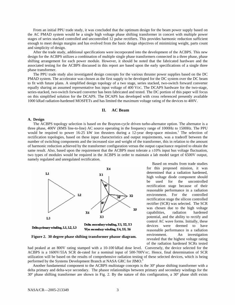
Figure 2. 30 degree phase shifting transformer phasor diagram.
Another fundamental component to the ACBPS multistage concepts is the 30º phase shifting transformer with a delta primary and delta-wye secondary. The phasor relationships between primary and secondary windings for the 30º phase shifting transformer are shown in Fig. 2. By the nature of this configuration, a 30º phase shift exists
3NASA/CR—2005-213349

between the outputs of delta and wye secondaries. This type of transformer configuration causes the triplen harmonics (multiples of three) to cancel in the primary whereas, the non-triplens cancel in the secondary. The number of three phase outputs determines the range of non-triplen harmonics to be canceled. Hence, the amount of harmonic component cancellation can be chosen in a precise manner. The triplen harmonics are the main cause of heat because they add together in the neutral conductor. This causes the neutral conductor to overheat because neutral conductors are designed with the same current carrying capacity as the phase conductors. The magnitude of the harmonic current produced by the triplens can approach twice the fundamental
phase current. The positive and negative sequenced harmonics acting upon each other create heat which leads to early failure. Transformers configured with a delta primary and a wye secondary inherently decrease the negative effects of harmonics. The triplen harmonics are not reflected and flow in the delta primary. To further explore the harmonics, the 12 pulse configurations were compared in both the controlled and uncontrolled schemes. The percent harmonic content in the uncontrolled module is shown in Fig. 3. This shows that the most predominant harmonic component is the 11th at 6% with the next largest being the 13th at 3%. The harmonic content in the controlled rectification is shown in Fig. 4. This shows that the most predominant harmonic component is also the 11th, but at 8%. The next largest is again the 13th at 6%. The fundamental difference between the two types of rectification topologies is the amount of ripple that will result primarily from the impact of the 11th and 13th harmonics.
5 7 11 13 17 19 23 25 29 31 35 370%1%2%3%4%5%6%7%8%
Perc
ent H
arm
onic
C
urre
ntHarmonic Current Components
Figure 4. SCR converter harmonics.
5 7 11 13 17 19 23 25 29 31 35 370%1%2%3%4%5%6%
Perc
e nt H
a rm
onic
C
urre
nt
Harmonic Current Components
Figure 3. Diode rectifier harmonics.
The initial transformer concept that was used for test report data, was a single unit, three phase transformer used to step up the input voltage and designed to supply all the modules. This specification was redefined later in the trade study due to the shear volumetric mass of such a transformer and the redefined secondary voltage. The transformers to be used in the full breadboard system involved multiple key decisions to be made on core selection, core type, temperature considerations, bobbin design, transformer volume, weight and isolation concerns. Hence, a trade study was conducted to document and present the findings to support the decisions to be made. The proposed replacement for the all-inclusive single transformer became multiple single phase transformers connected in the same configuration for each module. This approach will render a greater surface area to be used as shielding for the electronic components in the radiation environment and offer flexibility in packaging, while providing the same electrical performance. The configuration of the multiple single phase transformers in conjunction with the single stage uncontrolled system is shown in Fig. 5. The uncontrolled concept consists of a 3-phase, 30o phase shifting transformer, two high voltage six-pulse diode bridge rectifiers, and two smoothing capacitor banks to achieve the specified target voltage.5,6
Figure 5. Proposed configuration of a single module uncontrolled system.
4NASA/CR—2005-213349
Since simplicity in design was a high priority to reduce parts count, the uncontrolled stage honors the request. Here the AC input power is connected in parallel to the transformer inputs and the transformer outputs are connected, individually, to a pair of diode bridge rectifiers. The unfiltered DC outputs of the diode bridge rectifiers are smoothed by capacitors to meet the final specification. Finally, the dc output of each bridge is taken across the series connected smoothing capacitors adding the output voltages of each bridge forming the output voltage.
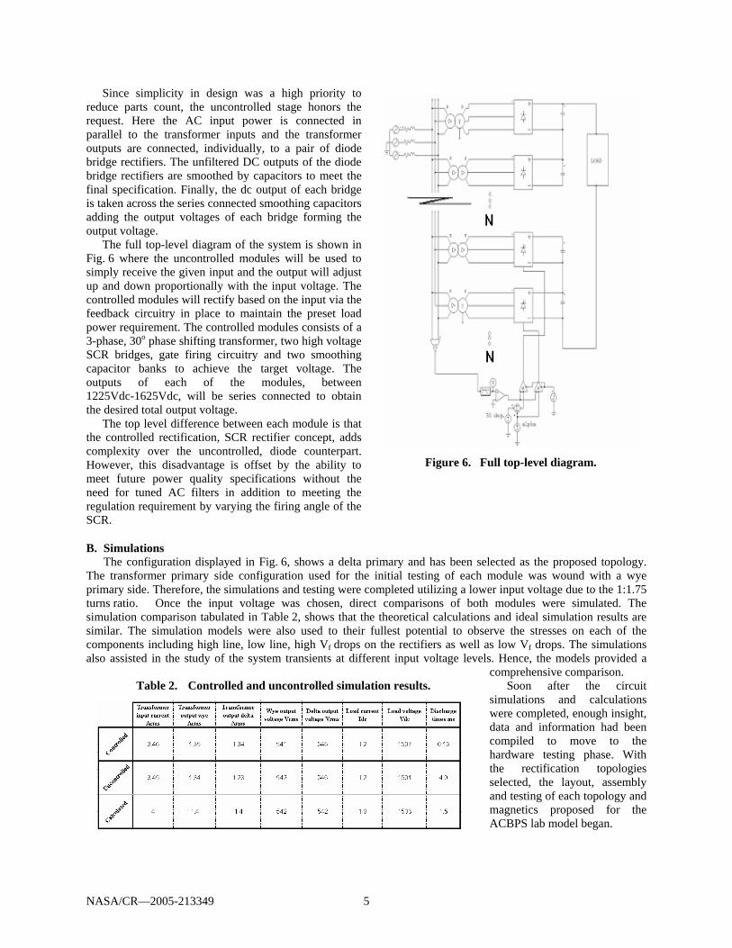
Figure 6. Full top-level diagram.
The full top-level diagram of the system is shown in Fig. 6 where the uncontrolled modules will be used to simply receive the given input and the output will adjust up and down proportionally with the input voltage. The controlled modules will rectify based on the input via the feedback circuitry in place to maintain the preset load power requirement. The controlled modules consists of a 3-phase, 30o phase shifting transformer, two high voltage SCR bridges, gate firing circuitry and two smoothing capacitor banks to achieve the target voltage. The outputs of each of the modules, between 1225Vdc-1625Vdc, will be series connected to obtain the desired total output voltage. The top level difference between each module is that the controlled rectification, SCR rectifier concept, adds complexity over the uncontrolled, diode counterpart. However, this disadvantage is offset by the ability to meet future power quality specifications without the need for tuned AC filters in addition to meeting the regulation requirement by varying the firing angle of the SCR.
B. Simulations The configuration displayed in Fig. 6, shows a delta primary and has been selected as the proposed topology. The transformer primary side configuration used for the initial testing of each module was wound with a wye primary side. Therefore, the simulations and testing were completed utilizing a lower input voltage due to the 1:1.75 turns ratio. Once the input voltage was chosen, direct comparisons of both modules were simulated. The simulation comparison tabulated in Table 2, shows that the theoretical calculations and ideal simulation results are similar. The simulation models were also used to their fullest potential to observe the stresses on each of the components including high line, low line, high Vf drops on the rectifiers as well as low Vf drops. The simulations also assisted in the study of the system transients at different input voltage levels. Hence, the models provided a
comprehensive comparison. Table 2. Controlled and uncontrolled simulation results.
Soon after the circuit simulations and calculations were completed, enough insight, data and information had been compiled to move to the hardware testing phase. With the rectification topologies selected, the layout, assembly and testing of each topology and magnetics proposed for the ACBPS lab model began.
5NASA/CR—2005-213349
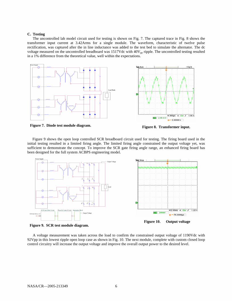
C. Testing The uncontrolled lab model circuit used for testing is shown on Fig. 7. The captured trace in Fig. 8 shows the transformer input current at 3.42Arms for a single module. The waveform, characteristic of twelve pulse rectification, was captured after the in line inductance was added to the test bed to simulate the alternator. The dc voltage measured on the uncontrolled breadboard was 1517Vdc with 40Vpp ripple. The uncontrolled testing resulted in a 1% difference from the theoretical value, well within the expectations.
45
6 1
2 3
Power Supply
1 2
3
4 5
6
Load Bank
Figure 7. Diode test module diagram.
Figure 8. Transformer input.
Figure 9 shows the open loop controlled SCR breadboard circuit used for testing. The firing board used in the initial testing resulted in a limited firing angle. The limited firing angle constrained the output voltage yet, was sufficient to demonstrate the concept. To improve the SCR gate firing angle range, an enhanced firing board has been designed for the full system ACBPS engineering model.
Load
45
6 1
2 3
54
321
121110
98
7
6
1 2
3
4 5
6
Power Supply
SCR Gate Drive Circuit Phase & Control Circuit
SCR Gate Drives 1-12
Attenuation Block
Output Voltage
Output Voltage
Figure 9. SCR test module diagram.
Figure 10. Output voltage
A voltage measurement was taken across the load to confirm the constrained output voltage of 1190Vdc with 92Vpp in this lowest ripple open loop case as shown in Fig. 10. The next module, complete with custom closed loop control circuitry will increase the output voltage and improve the overall output power to the desired level.
6NASA/CR—2005-213349

III. DC Accelerator
A. Design and Analysis The available stock of high voltage radiation-hardened semiconductor switches has influenced and controlled the
design of the accelerator power supply due to their scarcity in today’s market place. Therefore, the voltage rating of the radiation-hardened MOSFETs was the critical design constraint for the topology that has been incorporated. An assumption was made for concerns regarding design margin that the switch should be stressed at no more than 75% of its rated voltage. Presently, 1000 kRad high reliability MOSFETs with a Vds of 400V are available with reasonable Rdson specifications. As a result, the switches should experience no more than 300V in their off state and during transient switching. Since the assumed input voltage to the accelerator is 400VDC, a multiple stage approach to this supply will be necessary. Utilizing multiple stages in a series stacked configuration on the input allows for reduction in the voltage handling capabilities of the semiconductor switches. The number of stages should be minimized in order to maximize the reliability of the supply and minimize the parts count. In turn, to minimize the number of stages, a topology must be selected where the switch experiences the input voltage of the stage during the off-state. This requirement significantly restricts the number of topologies from which to choose, as many of the topologies used in switch mode power supplies expose the switches to twice the input voltage in their off-state. The full bridge and the two-switch forward are two converter topologies that meet the off-state voltage requirements as stated above. While both topologies meet these requirements, further investigation determined that the full bridge topology is more susceptible to switching voltage spikes. Conversely, the two-switch forward topology has the advantage that switching voltage transients are clamped to the input voltage. Additionally, the full bridge is more complex than the two-switch forward. As a result, the parts count of the full bridge is significantly higher per stage. Since the design is a series stack approach consisting of multiple stages, the parts count tends to increase rapidly. Hence, the proposed fundamental topology is the two-switch forward converter. This topology inherently yields reasonable efficiencies with minimal parts count. Figure 11 portrays an idealized two-switch forward converter that has been proposed for integration.
In any forward converter, the magnetization current of the transformer must be taken into account. Otherwise, the stored energy of the core would inevitably cause the converter to fail due to core saturation and/or meltdown. In the traditional forward converter, an additional demagnetizing winding and accompanying diode are required for proper demagnetization6. However, with the two-switch forward topology, the primary side diodes eliminate the need for the additional winding and
diode. When the switches are off, current flows in the direction of the diodes and the core is reset. Consequently, the maximum duty ratio of the converter is limited to no more than 50%. Therefore, to insure proper reset of the core, the duty ratio for this design is chosen to operate at 33% nominally to provide ample margin.
Figure 11. Idealized two-switch forward converter.
With a 400V input, a two series stacked two-switch forward converter will stand 200V input per stage, which stresses the input MOSFETs to a maximum 50% of their 400V rating. Additionally, the goal was to obtain the desired 800V output voltage in two output stages to further reduce parts count. However, in order to meet this constraint, a turns ratio of 1 to 6 is necessary as calculated from Eq. (1). 6
DVdVoN 1
×= (1)
7NASA/CR—2005-213349

Unfortunately, a large ratio is undesirable because it necessitates the use of substantially high voltage rated diodes. Also, switching at high frequency requires ultra fast diodes. Hence, a minimum requirement of 1600V rated
ultra fast diodes would be incurred. Currently, these devices are not readily available.
Therefore, the design has been modified to reduce the voltage stress on the diodes. By center-tapping the transformer secondary of each two-switch forward converter and series-stacking the secondary side rectifier stages provides a means to this end. Figure 12 illustrates this concept. 7
In this configuration, the voltage rating of the secondary side ultra fast diodes need only be 800V, 1-Mrad rating while concurrently providing the 400V output across the sum of the half stages. The entire system would then consist of two of these more complex stages as shown in Fig. 13.
An additional benefit of this design is that the entire system contains only four controlled switches. Since all of the switches would be turned on and off simultaneously, only one PWM chip operated in voltage-mode is required to control the entire supply. Although all four switches are at different potentials, a single gate drive circuit can be implemented via a five-filar wound isolated transformer. A significant advantage of this equal duty cycle control is that input voltage sharing is inherently forced between the two stages. As a result, the input capacitor voltages will tend to converge.
Figure 12. Center-tapping the transformer secondary and series-stacking two traditional forward converter secondary side semiconductors.
4
89
2
7 3
1 : N/2 : N/2
12
12
4
89
2
7 3
1 : N/2 : N/2
12
12
2
1
32
1
3
12
1 2
12
12
2
1
3
VoVd
2
1
3
1 2
12
12
12
Figure 13. Two stage, series stacked, two-switch forward converter.
B. Testing Preliminary testing of the DCAPS lab engineering model as shown in Fig. 13 was conducted with a system
input voltage of 100V and an output voltage of only 200V. Each input stage handled approximately 50V and each output stage handled approximately 100V. Figure 14 displays PWM controller output signal to the gate drive. A duty ratio of 33.40% is observed, as opposed to the theoretical 33.33%. Also depicted in Fig. 14 is the current of one of the return side inductors revealing that the converter is operating in continuous conduction mode as desired.
The output voltage ripple is another area of major interest. The actual output voltage as shown in Fig. 15 is 203V. The peak-to-peak ripple and noise as shown in Fig. 15 is 5.72 Vpp or 2.8% of the 203V. Both the output voltage regulation and peak-to-peak ripple are well within the desired 5% tolerance specification.
8NASA/CR—2005-213349

Figure 16. PWM and input MOSFET Vds. Channel 1 trace: PWM IC Output Channel 2 trace: Vds (50V/div)
Figure 14. PWM IC output and secondary inductor current.
Channel 1 trace: PWM IC Output Channel 3 trace: Secondary Inductor Current
Figure 15. PWM, output voltage (Vo) and output ripple voltage.
Channel 1 trace: PWM IC Output Channel 2 trace: Output Voltage Channel 4 trace: Output Ripple Voltage
The advantage of clamping of the input voltage to eliminate switching spikes is illustrated in Fig. 16. The figure portrays the Vds of one of the input MOSFETs. From the trace it is apparent that essentially no voltage spike transients are manifested during turn off and turn on. As predicted this waveform clearly shows that the voltage stress on the switch is almost precisely 50V, which is the input to the discrete converter with a 100V input voltage to the system. Preliminary testing of the DCAPS has provided results consistent with those theoretical results which have been predicted. Additional testing will be conducted to validate this design.
IV. Conclusion Outlined in this report were two discrete power
supplies, the AC Beam Power Supply and the DC Accelerator Power Supply, carried out under project
Prometheus. Any opinions expressed are those of the author(s) and do not necessarily reflect the views of Project Prometheus. The progress made in the switching topologies that have been proposed for JIMO PPU has been reported.
Regarding the ACBPS, two topologies, diode (uncontrolled) and SCR (controlled), will be utilized in order to meet the specified requirements of the proposed JIMO mission. A full 6.5kV ACBPS will be fabricated and tested and integrated with a thruster. Should the comprehensive radiation testing disqualify the SCR from consideration, MOSFET devices can be used. In this case, the output voltage of the control stage would have to be reduced due to the lower blocking voltage of the MOSFET.
Regarding the DCAPS, numerous solutions were initially analyzed. In an effort to minimize the total parts count and the number of stages, the two-switch forward converter has been chosen as the primary topology of interest. A two stage, series-stacked, two-switch forward approach was necessary in order to meet specifications and was examined as the focus of this paper. A breadboard version of the supply was fabricated. Preliminary testing was performed and the results were promising. Full input/output voltage testing and characterization of the supply will be conducted in the near future. In addition, the DCAPS will be modified for fault shutdown and other issues.
9NASA/CR—2005-213349

References 1Kimnach, G. L., and Soltis, J.V. “Power Management and Distribution Trades Studies for a Deep-space Mission Scientific
Spacecraft,” Space Technology and Applications International Forum – STAIF 2004. 2Foster, J., “Jupiter Icy Moons Orbiter (JIMO) HiPEP Phase 1 Study Report for FY 2003,” NASA Glenn Research Center,
September 30, 2003. 3J.E. Polk, J.E, “Jupiter Icy Moons Orbiter (JIMO) Nuclear Electric Xenon Ion System (NEXIS) Phase 1 Final Report,”
Section 353, JPL , October 1, 2003. 4Dr. Rohal, Patton, Dr. Blue, “GRC Follow on in Reactor and 60Co Irradiation Characterization Test Report”, NASA Glenn
Research Center, 2004. 5Ralph E. Tarter, Solid-State Power Conversion Handbook, John Wiley, 1993. 6Mohan, Undeland, Robbins, Power Electronics Converters, Applications, and Design 2nd ed. John Wiley, 1995.
7Pressman, Abraham, Switching Power Supply Design 2nd ed, McGraw-Hill, 1998.
10NASA/CR—2005-213349

This publication is available from the NASA Center for AeroSpace Information, 301–621–0390.
REPORT DOCUMENTATION PAGE
2. REPORT DATE
19. SECURITY CLASSIFICATION OF ABSTRACT
18. SECURITY CLASSIFICATION OF THIS PAGE
Public reporting burden for this collection of information is estimated to average 1 hour per response, including the time for reviewing instructions, searching existing data sources,gathering and maintaining the data needed, and completing and reviewing the collection of information. Send comments regarding this burden estimate or any other aspect of thiscollection of information, including suggestions for reducing this burden, to Washington Headquarters Services, Directorate for Information Operations and Reports, 1215 JeffersonDavis Highway, Suite 1204, Arlington, VA 22202-4302, and to the Office of Management and Budget, Paperwork Reduction Project (0704-0188), Washington, DC 20503.
NSN 7540-01-280-5500 Standard Form 298 (Rev. 2-89)Prescribed by ANSI Std. Z39-18298-102
Form ApprovedOMB No. 0704-0188
12b. DISTRIBUTION CODE
8. PERFORMING ORGANIZATION REPORT NUMBER
5. FUNDING NUMBERS
3. REPORT TYPE AND DATES COVERED
4. TITLE AND SUBTITLE
6. AUTHOR(S)
7. PERFORMING ORGANIZATION NAME(S) AND ADDRESS(ES)
11. SUPPLEMENTARY NOTES
12a. DISTRIBUTION/AVAILABILITY STATEMENT
13. ABSTRACT (Maximum 200 words)
14. SUBJECT TERMS
17. SECURITY CLASSIFICATION OF REPORT
16. PRICE CODE
15. NUMBER OF PAGES
20. LIMITATION OF ABSTRACT
Unclassified Unclassified
Final Contractor Report
Unclassified
1. AGENCY USE ONLY (Leave blank)
10. SPONSORING/MONITORING AGENCY REPORT NUMBER
9. SPONSORING/MONITORING AGENCY NAME(S) AND ADDRESS(ES)
National Aeronautics and Space AdministrationWashington, DC 20546–0001
Available electronically at http://gltrs.grc.nasa.gov
March 2005
NASA CR—2005-213349AIAA–2004–3452
E–14817
WBS–22–973–80–60NAS3–00145
16
Power Processing for a Conceptual Project Prometheus ElectricPropulsion System
Joseph E. Scina, Jr., Michael Aulisio, Scott S. Gerber, Frank Hewitt,Leonard Miller, and Malik Elbuluk
Power processing unit; Electric propulsion; Ion thruster
Unclassified -UnlimitedSubject Categories: 20 and 33 Distribution: Nonstandard
ZIN Technologies, Inc.3000 Aerospace ParkwayBrook Park, Ohio 44142
Prepared for the 40th Joint Propulsion Conference and Exhibit cosponsored by the AIAA, ASME, SAE, and ASEE,Fort Lauderdale, Florida, July 11–14, 2004. Joseph E. Scina, Jr., Michael Aulisio, Scott S. Gerber, Frank Hewitt, andLeonard Miller, ZIN Technologies, Inc., Brook Park, Ohio 44142; and Malik Elbuluk, University of Akron, Akron,Ohio 44235. Project Manager, Luis R. Piñero, Power and On-Board Propulsion Technology Division, NASA GlennResearch Center, organization code 5430, 216–977–7428.
NASA has proposed a bold mission to orbit and explore the moons of Jupiter. This mission, known as the Jupiter IcyMoons Orbiter (JIMO), would significantly increase NASA’s capability to explore deep space by making use of highpower electric propulsion. One electric propulsion option under study for JIMO is an ion propulsion system. An earlyversion of an ion propulsion system was successfully used on NASA’s Deep Space 1 mission. One concept for an ionthruster system capable of meeting the current JIMO mission requirement would have individual thrusters that are16 to 25 kW each and require voltages as high as 8.0 kV. The purpose of this work is to develop power processingschemes for delivering the high voltage power to the spacecraft ion thrusters based upon a three-phase AC distributionsystem. In addition, a proposed DC-DC converter topology is presented for an ion thruster ancillary supply basedupon a DC distribution system. All specifications discussed in this paper are for design convenience and are speculativein nature.