Power MOSFET Selecting MOSFFETs and Consideration for ...
18
Power MOSFET Selecting MOSFFETs and Consideration for Circuit Design Application Note 2018-07-26 1 © 2017 - 2018 Toshiba Electronic Devices & Storage Corporation Description This document explains selecting MOSFETs and what we have to consider for designing MOSFET circuit, such as temperature characteristics, effects of wire inductance, parasitic oscillations, avalanche ruggedness, and snubber circuit. Power MOSFET Selecting MOSFFETs and Consideration for Circuit Design
Transcript of Power MOSFET Selecting MOSFFETs and Consideration for ...

Power MOSFET Selecting MOSFFETs and Consideration for Circuit Design Application Note
2018-07-26 1 © 2017 - 2018 Toshiba Electronic Devices & Storage Corporation
Description This document explains selecting MOSFETs and what we have to consider for designing MOSFET circuit, such as temperature characteristics, effects of wire inductance, parasitic oscillations, avalanche ruggedness, and snubber circuit.
Power MOSFET Selecting MOSFFETs and Consideration
for Circuit Design

Power MOSFET Selecting MOSFFETs and Consideration for Circuit Design Application Note
2018-07-26 2 © 2017 - 2018 Toshiba Electronic Devices & Storage Corporation
Table of Contents Description ............................................................................................................................................ 1
Table of Contents ................................................................................................................................. 2
1. Selecting MOSFETs .......................................................................................................................... 3
1.1. Voltage and Current Ratings .............................................................................................................. 3
1.2. Considerations for VGS......................................................................................................................... 3
1.3. Switching Speed .................................................................................................................................. 4
2. Considerations for MOSFET Circuit Design ................................................................................... 5
2.1. Temperature Characteristics of Power MOSFETs ............................................................................ 5
2.2. Switching Time and Drive Conditions .............................................................................................. 6
2.3. Effects of Wire Inductance ................................................................................................................. 6
2.4. Parasitic Oscillations ............................................................................................................................ 7
2.5. Use of a Source-Drain Diode ............................................................................................................. 8
2.6. Avalanche Ruggedness ....................................................................................................................... 9
2.7. Parallel Connections .......................................................................................................................... 10
2.8. Snubber Circuit ...................................................................................................................................11
2.8.1. Snubber for a flyback converter ....................................................................................................... 11
2.8.2. General turn-off snubber ...................................................................................................................14
RESTRICTIONS ON PRODUCT USE.................................................................................................. 18

Power MOSFET Selecting MOSFFETs and Consideration for Circuit Design Application Note
2018-07-26 3 © 2017 - 2018 Toshiba Electronic Devices & Storage Corporation
1. Selecting MOSFETs MOSFETs with appropriate ratings and characteristics should be selected according to the applications in which they will be used.
1.1. Voltage and Current Ratings The drain-source voltage VDSS rating is important in selecting MOSFETs. Application of a voltage
exceeding VDSS might result in the destruction of a MOSFET. It is necessary to choose MOSFETs with a VDSS sufficiently higher than the voltage at which they will actually be used. However, MOSFETs with high VDSS ratings tend to have large on-state resistance, RDS(ON). A downside of using such MOSFETs is increased conduction loss. If you select MOSFETs according to possible peak surge voltage, you could end up opting for devices with large on-state resistance. To address this situation, Toshiba also provides MOSFETs with guaranteed tolerance against avalanche breakdown current or energy in the event that a surge voltage exceeding the voltage rating forces a MOSFET into the breakdown region. Such MOSFETs feature a low VDSS and low on-state resistance. Generally, on-state resistance determines the upper limit of the drain current ID. Ensure that not only the loss calculated as ID2×RDS(ON), the permissible power dissipation but also a temperature rise due to heating does not cause the device to exceed its operating temperature range.
1.2. Considerations for VGS The conditions governing VGS are also important factors for the selection of MOSFETs. Drain current, RDS(ON) and gate voltage are described below:
(1) The on-state resistance of MOSFETs is low when they operate in the linear region (i.e., at a voltage lower than pinch-off voltage). Therefore, for switching applications, you can reduce the on-state resistance by using MOSFETs in the low VDS region (Figure 1.1). This helps reduce power loss. Note that the amount of current that MOSFETs can handle is limited by the value of VGS.
(2) MOSFETs turn on when the gate-source voltage VGS exceeds their threshold voltage Vth (Figure 1.2). It is therefore necessary to choose a value for VGS that is sufficiently higher than Vth. There is a tendency that the higher the VGS, the lower the RDS(ON) value becomes. Also, the higher the temperature, the higher the RDS(ON) value becomes (Figure 1.3). In order to reduce loss, it is important to increase VGS in order to minimize the resistance of the device at the current level at which it is used (Figure 1.4). Conversely, a high VGS value increases the drive loss at light loads for high frequency switching. Selecting the optimal gate voltage is therefore critical.
(3) Generally, it is recommended to drive the gate of many power MOSFET at a VGS of 10 V. Toshiba's product portfolio also includes power MOSFETs designed for gate drive at a VGS of 4.5 V. Select the power MOSFET that best suits your equipment requirements.
Figure 1.1 Operating Regions of a MOSFET

Power MOSFET Selecting MOSFFETs and Consideration for Circuit Design Application Note
2018-07-26 4 © 2017 - 2018 Toshiba Electronic Devices & Storage Corporation
1.3. Switching Speed
When a power MOSFET switches at a high frequency, its switching loss accounts for a significant portion of total loss. To reduce total loss for high frequency switching applications, high speed power MOSFETs should be used. In our power MOSFETs lineup, in the case of products were classified in low RDS(on) type and high speed type, choose the MOSFETs depend on the application . However if they are not classified, it needs to adjust switching speed by setting output impedance of driving circuit.
Figure 1.2 ID-VGS Curves Figure 1.3 RDS(ON)-Temperature Curves Figure 1.4 VDS-VGS Curves

Power MOSFET Selecting MOSFFETs and Consideration for Circuit Design Application Note
2018-07-26 5 © 2017 - 2018 Toshiba Electronic Devices & Storage Corporation
2. Considerations for MOSFET Circuit Design 2.1. Temperature Characteristics of Power MOSFETs
The forward transfer admittance |Yfs| of a power MOSFET is given by a differential coefficient of
the ID – VGS curve shown in Figure 2.1. The temperature coefficient of forward transfer admittance becomes negative in the high current region. Even if large drain current is about to flow due to output change, an increase in internal channel temperature causes forward transfer admittance to decrease, making a power MOSFET less prone to a catastrophic failure due to current concentration and thermal runaway. What needs to be considered in the use of a power MOSFET is the temperature dependency of drain-source on-state resistance RDS(ON) (Figure 2.2). The temperature coefficient of RDS(ON) varies with the withstand voltage and the manufacturing process of the device. See the appropriate technical datasheet for details. It is therefore necessary to take the temperature dependency of RDS(ON) into consideration in order to select a heat sink with appropriate thermal resistance.
Figure 2.1 ID – VGS Curves Figure 2.2 RDS(ON) – Tc Curves

Power MOSFET Selecting MOSFFETs and Consideration for Circuit Design Application Note
2018-07-26 6 © 2017 - 2018 Toshiba Electronic Devices & Storage Corporation
2.2. Switching Time and Drive Conditions Bipolar transistors need a large base current to maintain low on-state voltage. In contrast, since power MOSFETs are voltage-controlled devices, they can be driven just by charging gate capacity, and are therefore a low in power consumption. Note, however, that power MOSFETs have a slightly large input capacitance Ciss. Thus, for high speed switching applications, it is necessary to quickly charge the input capacitance from a low-impedance signal source. Low-impedance drive is required to reduce turn-on time. However, the use of a high gate voltage results in the much charging of gate-source capacitance, resulting in an increase in td
(off). Switching time can be controlled via gate resistance. If you want to change the turn-on and turn-off switching speeds separately, you can use diodes to change the gate resistance values for turn-on and turn-off. Figure 2.3 shows some examples.
Figure 2.3 Drive Circuit Examples 2.3. Effects of Wire Inductance
Since the switching time of power MOSFETs is more than an order of magnitude lower than that of bipolar transistors, power MOSFETs are ideal for high speed switching applications. However, because of high speed switching performance, a circuit design should be safeguarded against voltage surges so that an excessive surge caused by stray inductances, LS and LS’, will not be
applied to the MOSFET. The surge voltage Vsurge resulting from stray inductances is calculated as follows:
𝑉𝑉𝑠𝑠𝑠𝑠𝑠𝑠𝑠𝑠𝑠𝑠 = −(𝐿𝐿𝑆𝑆 + 𝐿𝐿𝑆𝑆′) ∙𝑑𝑑𝑑𝑑𝑑𝑑𝑑𝑑
+ 𝑉𝑉𝐷𝐷𝐷𝐷
It is necessary to ensure that drain-source breakdown voltage VDSS will never be exceeded even
in the presence of Vsurge. Vsurge can be decreased by reducing di/dt and stray inductances. Since you do not want to reduce di/dt for high speed switching applications, reducing stray
(a) (b) (C) On-state gate resistance: R1 Off-state gate resistance: R2
VDD
RL
GND
R1
R2
VDD
RL
GND
R1
R2
On-state gate resistance: R1 and R2 in parallel
Off-state gate resistance: R2
On-state gate resistance: R2 Off-state gate resistance:
R1 and R2 in parallel
VDD
RL
GND
R1
R2

Power MOSFET Selecting MOSFFETs and Consideration for Circuit Design Application Note
2018-07-26 7 © 2017 - 2018 Toshiba Electronic Devices & Storage Corporation
inductances are effective. For example, inserting a capacitor as shown in Figure 2.4. is effective to reduce stray inductances.
Figure 2.4 Stray Inductances of a Circuit and the Measure
2.4. Parasitic Oscillations
Power MOSFETs are more prone to parasitic oscillations than bipolar transistors because of the MOSFET’s advantage of high gain in the high frequency domain. A power MOSFET goes into parasitic oscillation when the coupling between input and output increases due to gate-drain capacitance Crss and parasitic wire capacitance Cs causing negative impedance at the input. Several measures are used to prevent parasitic oscillation: • Use thick, short wires, or use twisted wires to prevent the coupling between two wires. • Insert a ferrite bead as close to the gate terminal as possible. • Insert a series resistor in the gate terminal.
Figure 2.5 Prevention of Parasitic Oscillation
Insert a resistor to reduce the gain.
Insert a ferrite bead.
Use thick, short wires.
Cs

Power MOSFET Selecting MOSFFETs and Consideration for Circuit Design Application Note
2018-07-26 8 © 2017 - 2018 Toshiba Electronic Devices & Storage Corporation
2.5. Use of a Source-Drain Diode Typical motor control circuits use power MOSFETs in a bridge configuration and alternately turn on and off the MOSFETs upper and lower arms. When power MOSFETs Q1 and Q4 in Figure 2.6 are turned on, a current flows through the circuit,
as indicated by A. Next, when MOSFET Q1 is turned off to control the motor speed, a current
circulates through the body diode in MOSFET Q2 as indicated by B. When MOSFET Q1 is turned
on thereafter, a short-circuit current flows from Q1 to MOSFET Q2 as shown by C during the
reverse recovery time trr of the body diode of Q2. The resulting loss generates heat. Therefore,
power MOSFETs having a body diode with a short trr are desirable for motor control applications. Although body diodes in power MOSFETs can be used as flywheel diodes, MOSFETs with a high speed diode are commonly used for this purpose. In some cases, you can connect a Schottky barrier diode (SBD) in series with a power MOSFET in order to nullify the effect of the body diode in a MOSFET and instead add an external fast-recovery diode (FRD) in parallel with the MOSFET, as shown in Figure 2.7.
M
Q1
Q2
Q3
Q4
FRD
SBD
Figure 2.7 Adding External Diodes
Figure 2.6 Motor Control Circuitry Using Power MOSFETs
Current A
Current B Short-circuit current C (Reverse Recovery Current)

Power MOSFET Selecting MOSFFETs and Consideration for Circuit Design Application Note
2018-07-26 9 © 2017 - 2018 Toshiba Electronic Devices & Storage Corporation
2.6. Avalanche Ruggedness Power MOSFETs are commonly used as high speed switching devices. A power MOSFET experiences a high voltage spike between drain and source during device turn-off due to circuit inductance and stray inductances. Sometimes, the spike voltage exceeds the ratings of the MOSFET. Conventionally, a surge absorber circuit was used to protect electronic devices. Today, surge absorber circuits are dispensed with in order to reduce the number of parts and thereby the size of the system. To address this requirement, a power MOSFET needs to damp avalanche energy even in the event of a voltage surge exceeding its voltage ratings. In response, Toshiba now provides a product series that can safely operate at up to the self-breakdown voltage as long as avalanche ruggedness conditions are met. Avalanche events place an excessive stress on the MOSFET. Therefore, even if the avalanche capability is guaranteed, it is recommended to ensure that power MOSFETs will not go into avalanche mode for the sake of system reliability. Note that many MOSFETs do not provide any guarantee for repetitive avalanche ruggedness. For automotive and other safety-critical applications, we urged you to ensure that power MOSFETs, even those with a maximum avalanche energy rating, will not enter avalanche mode. Refer the individual datasheets for details. • Avalanche energy calculation
Avalanche energy is calculated as:
𝐸𝐸𝐴𝐴𝑆𝑆 =12𝐿𝐿𝐼𝐼𝐴𝐴𝑆𝑆2
𝐵𝐵𝑉𝑉𝐷𝐷𝑆𝑆𝑆𝑆𝐵𝐵𝑉𝑉𝐷𝐷𝑆𝑆𝑆𝑆 − 𝑉𝑉𝐷𝐷𝐷𝐷
EAS: Avalanche energy
IAS: Avalanche current
BVDSS: Drain-source breakdown voltage
VDD: Supply voltage Avalanche ruggedness is the energy allowable in a single pulse. The maximum channel temperature, Tch(max), is specified so that the rated avalanche current IAS will not be exceeded when single-shot avalanche energy is applied under the prescribed conditions. In practice, an increase in temperature caused by an avalanche event is calculated in order to determine that the channel temperature will not exceed the rated Tch(max) value even after ambient temperature, while taking into account a possible rise in temperature caused by steady-state operation and switching losses. The temperature increase in avalanche mode is estimated as follows:
∆𝑇𝑇𝑐𝑐ℎ = 0.473 ∙ 𝐵𝐵𝑉𝑉𝐷𝐷𝑆𝑆𝑆𝑆 ∙ 𝐼𝐼𝐴𝐴𝑆𝑆 ∙ 𝑟𝑟𝑡𝑡ℎ(𝑐𝑐ℎ−𝑐𝑐) (𝑁𝑁𝑁𝑁𝑑𝑑𝑁𝑁) BVDSS: Drain-source breakdown voltage
IAS: Avalanche current
rth(ch-c): Transient channel-to-case thermal resistance in avalanche mode

Power MOSFET Selecting MOSFFETs and Consideration for Circuit Design Application Note
2018-07-26 10 © 2017 - 2018 Toshiba Electronic Devices & Storage Corporation
Note: Power dissipation PD caused by the current and voltage waveforms shown in Figure 2.8 changes over time in the shape of a triangle as highlighted by oblique lines in Figure 2.9. At this time, the channel temperature changes as indicated by the solid line in Figure 2.9, and peaks at time 1/2 tw. The maximum channel temperature at 1/2 tw is calculated as 0.699 times the channel temperature change caused by the square wave. Hence, the approximate increase in channel temperature is as follows:
∆𝑇𝑇𝑐𝑐ℎ ≅ 0.669 ∙ 𝐵𝐵𝑉𝑉𝐷𝐷𝑆𝑆𝑆𝑆 ∙ 𝐼𝐼𝐴𝐴𝑆𝑆 ∙ 𝑟𝑟𝑡𝑡ℎ(12𝑑𝑑𝑤𝑤)
𝑟𝑟𝑡𝑡ℎ(12𝑑𝑑𝑤𝑤) ≅
1√2
𝑟𝑟𝑡𝑡ℎ(𝑑𝑑𝑤𝑤)
which can be restated as:
∆𝑇𝑇𝑐𝑐ℎ ≅ 0.669 ∙1√2
∙ 𝐵𝐵𝑉𝑉𝐷𝐷𝑆𝑆𝑆𝑆 ∙ 𝐼𝐼𝐴𝐴𝑆𝑆 ∙ 𝑟𝑟𝑡𝑡ℎ(𝑑𝑑𝑤𝑤)
≅ 0.473 ∙ 𝐵𝐵𝑉𝑉𝐷𝐷𝑆𝑆𝑆𝑆 ∙ 𝐼𝐼𝐴𝐴𝑆𝑆 ∙ 𝑟𝑟𝑡𝑡ℎ(𝑑𝑑𝑤𝑤)
2.7. Parallel Connections Power MOSFETs have outstanding thermal stability and do not suffer thermal runaway; therefore, connecting them in parallel is easier than with bipolar transistors. Bipolar transistors are operated by the flow of a base current; therefore, the current balance is disrupted by fluctuations of the base-emitter voltage VBE, making parallel connections difficult. Power MOSFTs, on the other hand, are voltage driven. Therefore it is only necessary to supply drive voltage to each FET connected in parallel, making parallel connection relatively easy. However, when controlling high power at high speeds, it is necessary to carefully consider selection of devices and the range of possible variations in their characteristics. The most important thing to remember when making parallel connections is to avoid current concentration, including overcurrent, and to assure a well-balanced, uniform flow of current to all devices under all possible load conditions. Normally, current imbalance appears during power-on and power-off; however, this is caused by differences in the switching times of the power MOSFET. It is known that variations in
Figure 2.8 Current and Voltage Waveforms Figure 2.9 Power Dissipation PD

Power MOSFET Selecting MOSFFETs and Consideration for Circuit Design Application Note
2018-07-26 11 © 2017 - 2018 Toshiba Electronic Devices & Storage Corporation
switching times are largely dependent on the value of the gate-source threshold voltage Vth.
That is, the smaller the value of Vth the faster the power-on time. Conversely, during power-off,
the larger the value of Vth, the faster the cutoff. Because of this, current imbalance occurs
during both power-on and power-off when the current concentrates in an FET with a small Vth. This current imbalance can apply an excessive power loss of a device and result in failure. For parallel connections, using of power MOSFETs with close values of Vth is preferable in order to reduce variations in switching time during transient periods. It is also important to insert a gate resistor between each power MOSFET connected in parallel to ensure stable operation and prevent abnormal oscillation.(Figure 2.10)
Figure 2.10 Parallel Connection
2.8. Snubber Circuit
Snubber circuits provide protection against transient voltages that occur during turn-off. Generally, a simple RC snubber uses a resistor R in series with a capacitor C. The RC snubber is connected in parallel with a power MOSFET. Cutting off a current in a circuit causes its voltage to increase sharply due to stray inductances. The snubber damps this surge voltage to protect the power MOSFET as well as components in its vicinity.
2.8.1. Snubber for a flyback converter
Transformers for flyback converters have leakage inductance Lleak. Leakage inductance causes a surge voltage to be applied instantaneously across the drain and source terminals of a power MOSFET when the MOSFET turn off. In the worst-case scenario, the surge voltage results in the destruction of the MOSFET. Snubbers for flyback converters are commonly composed of a diode D and an RC network (Figure 2.11 (a)). The RCD snubber is designed to reduce the effect of parasitic factors that cause a voltage surge. The circuit shown in Figure 2.11 (b) is not a snubber circuit; rather, it is a surge absorber using a clamp circuit.
ID2
Caused by
ID1 ID2 Q2
Isolate input and output signals.
It is advisable to place and route a circuit symmetrically.
0
0
ID1
ID2
Caused by (Vth of Q1 ) < (Vth of Q2 )

Power MOSFET Selecting MOSFFETs and Consideration for Circuit Design Application Note
2018-07-26 12 © 2017 - 2018 Toshiba Electronic Devices & Storage Corporation
Figure 2.11 Leakage Inductance of a Flyback Converter
(a) RCD snubber (b) Clamp Circuit Using a Zener Diode

Power MOSFET Selecting MOSFFETs and Consideration for Circuit Design Application Note
2018-07-26 13 © 2017 - 2018 Toshiba Electronic Devices & Storage Corporation
(1) RCD snubber An RDC snubber should be designed as follows. Choose a sufficiently large value for Csn so that current ringing during switching can be ignored. Immediately after a MOSFET is turned off, current IO flows into the secondary coil of the transformer. Vds becomes equal to Vin+nVo. (Where, n is the turn ratio, and nVo is the voltage induced across the primary coil by a current flowing through the secondary coil.) Vds causes a current isn to flow through the diode Dsn. The
voltage across Lleak becomes equal to Vclamp-nVo. At this time, isn is given by: 𝑑𝑑𝑑𝑑𝑠𝑠𝑠𝑠𝑑𝑑𝑑𝑑
= −𝑉𝑉𝑐𝑐𝑐𝑐𝑐𝑐𝑐𝑐𝑐𝑐 − 𝑛𝑛𝑉𝑉𝑜𝑜
𝐿𝐿𝑐𝑐𝑠𝑠𝑐𝑐𝑙𝑙
From this equation, the period of time ts during which isn continues flowing is calculated as
follows (where, ipeak is the peak current that occurs when the MOSFET is turned off.)
𝑑𝑑𝑠𝑠 =𝐿𝐿𝑐𝑐𝑠𝑠𝑐𝑐𝑙𝑙
𝑉𝑉𝑐𝑐𝑐𝑐𝑐𝑐𝑐𝑐𝑐𝑐 − 𝑛𝑛𝑉𝑉𝑜𝑜× 𝑑𝑑𝑐𝑐𝑠𝑠𝑐𝑐𝑙𝑙
The power dissipated by the snubber is:
𝑃𝑃𝑠𝑠𝑠𝑠 = 𝑉𝑉𝑐𝑐𝑐𝑐𝑐𝑐𝑐𝑐𝑐𝑐 ∙𝑑𝑑𝑐𝑐𝑠𝑠𝑐𝑐𝑙𝑙 ∙ 𝑑𝑑𝑠𝑠
2∙ 𝑓𝑓𝑠𝑠
(where, fs is the frequency, and (ipeak ∙ ts)/2] ∙ fs is the current.) Substituting ts into this equation gives:
𝑃𝑃𝑠𝑠𝑠𝑠 =12𝐿𝐿𝑐𝑐𝑠𝑠𝑐𝑐𝑙𝑙 ∙ 𝑑𝑑𝑐𝑐𝑠𝑠𝑐𝑐𝑙𝑙2 ∙
𝑉𝑉𝑐𝑐𝑐𝑐𝑐𝑐𝑐𝑐𝑐𝑐
𝑉𝑉𝑐𝑐𝑐𝑐𝑐𝑐𝑐𝑐𝑐𝑐 − 𝑛𝑛𝑉𝑉𝑜𝑜∙ 𝑓𝑓𝑠𝑠
Psn needs to be consumed by Rsn Hence, since 𝑉𝑉𝑐𝑐𝑐𝑐𝑐𝑐𝑐𝑐𝑐𝑐2
𝑅𝑅𝑠𝑠𝑠𝑠=
12𝐿𝐿𝑐𝑐𝑠𝑠𝑐𝑐𝑙𝑙 ∙ 𝑑𝑑𝑐𝑐𝑠𝑠𝑐𝑐𝑙𝑙2 ∙
𝑉𝑉𝑐𝑐𝑐𝑐𝑐𝑐𝑐𝑐𝑐𝑐
𝑉𝑉𝑐𝑐𝑐𝑐𝑐𝑐𝑐𝑐𝑐𝑐 − 𝑛𝑛𝑉𝑉𝑜𝑜∙ 𝑓𝑓𝑠𝑠
Rsn is calculated as:
𝑅𝑅𝑠𝑠𝑠𝑠 =2𝑉𝑉𝑐𝑐𝑐𝑐𝑐𝑐𝑐𝑐𝑐𝑐(𝑉𝑉𝑐𝑐𝑐𝑐𝑐𝑐𝑐𝑐𝑐𝑐 − 𝑛𝑛𝑉𝑉𝑜𝑜)
𝐿𝐿𝑐𝑐𝑠𝑠𝑐𝑐𝑙𝑙 ∙ 𝑑𝑑𝑐𝑐𝑠𝑠𝑐𝑐𝑙𝑙2 ∙ 𝑓𝑓𝑠𝑠
The snubber capacitance Csn should be considered, based on the ripple voltage of the snubber ΔVclamp. Ripple voltage is calculated as follows:
∆𝑉𝑉𝑐𝑐𝑐𝑐𝑐𝑐𝑐𝑐𝑐𝑐 =𝑉𝑉𝑐𝑐𝑐𝑐𝑐𝑐𝑐𝑐𝑐𝑐
𝐶𝐶𝑠𝑠𝑠𝑠 ∙ 𝑅𝑅𝑠𝑠𝑠𝑠 ∙ 𝑓𝑓𝑠𝑠
𝑪𝑪𝒔𝒔𝒔𝒔 =𝑽𝑽𝒄𝒄𝒄𝒄𝒄𝒄𝒄𝒄𝒄𝒄
∆𝑽𝑽𝒄𝒄𝒄𝒄𝒄𝒄𝒄𝒄𝒄𝒄 ∙ 𝑹𝑹𝒔𝒔𝒔𝒔 ∙ 𝒇𝒇𝒔𝒔
(2) Clamp circuitry using a Zener diode When a Zener diode is used in a clamp circuit, the Zener clamp voltage, Vz, should be chosen based on a voltage Vmax sufficiently lower than the maximum switching voltage of the MOSFET and the input voltage Vin.
Vz=Vmax – Vin The power dissipated by the Zener diode can be calculated in the same manner as for the RCD snubber:
𝑃𝑃𝑍𝑍 =12𝐿𝐿𝑐𝑐𝑠𝑠𝑐𝑐𝑙𝑙 ∙ 𝑑𝑑𝑐𝑐𝑠𝑠𝑐𝑐𝑙𝑙2 ∙
𝑉𝑉𝑐𝑐𝑐𝑐𝑐𝑐𝑐𝑐𝑐𝑐
𝑉𝑉𝑐𝑐𝑐𝑐𝑐𝑐𝑐𝑐𝑐𝑐 − 𝑛𝑛𝑉𝑉𝑜𝑜∙ 𝑓𝑓𝑠𝑠

Power MOSFET Selecting MOSFFETs and Consideration for Circuit Design Application Note
2018-07-26 14 © 2017 - 2018 Toshiba Electronic Devices & Storage Corporation
This equation shows that if Vclamp – nVo is too low, the power dissipation of the Zener diode increases sharply.
2.8.2. General turn-off snubber Surge voltage is produced by stray inductances of a circuit. A snubber should be connected in parallel with a switching device to absorb the surge voltage. There are two types of snubbers: one added across each switching device and a lumped snubber added across a power bus for all switching devices.
(1) Snubbers added to each switching device Cutting off the current in a circuit causes its voltage to increase sharply. Snubbers are designed to reduce a surge voltage to protect a switching device and its surrounding electronic devices.
a. RC snubber circuit ● Ideal for chopper circuits ● The power loss caused by an RC snubber resistor is so large that an RC
snubber is not suitable for high frequency switching applications. ● An RC snubber for a high capacitance switching device needs to have
a resistor with a small value, which causes drain current to increase during turn-on. ● The power P dissipated by the snubber resistor is calculated as follows:
P = 𝐶𝐶𝑠𝑠 ∙ 𝐸𝐸𝑑𝑑2 ∙ 𝑓𝑓
b. RDC charge-discharge snubber ● A diode can be added to the RC snubber to increase snubber resistance.
This makes it possible to eliminate a current to be shared by switching devices during turn-on.
● The large power dissipated by the snubber resistor makes an RDC snubber unsuitable for high frequency applications.
● The power dissipated by the snubber resistor is calculated as follows:
P =𝐿𝐿 ∙ 𝐼𝐼𝑜𝑜2 ∙ 𝑓𝑓
2+𝐶𝐶𝑠𝑠 ∙ 𝐸𝐸𝑑𝑑2 ∙ 𝑓𝑓
2
Figure 2.12 RC Snubber
Figure 2.13 RCD Charge-Discharge Snubber
Power MOSFET Selecting MOSFFETs and Consideration for Circuit Design Application Note
2018-07-26 15 © 2017 - 2018 Toshiba Electronic Devices & Storage Corporation
Figure 2.14 Discharge-Suppressing RCD Snubber
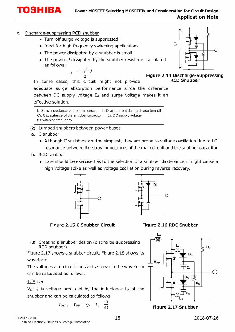
c. Discharge-suppressing RCD snubber
● Turn-off surge voltage is suppressed. ● Ideal for high frequency switching applications. ● The power dissipated by a snubber is small. ● The power P dissipated by the snubber resistor is calculated
as follows:
P =𝐿𝐿 ∙ 𝐼𝐼𝑜𝑜2 ∙ 𝑓𝑓
2
In some cases, this circuit might not provide adequate surge absorption performance since the difference between DC supply voltage Ed and surge voltage makes it an effective solution.
(2) Lumped snubbers between power buses a. C snubber
● Although C snubbers are the simplest, they are prone to voltage oscillation due to LC resonance between the stray inductances of the main circuit and the snubber capacitor.
b. RCD snubber ● Care should be exercised as to the selection of a snubber diode since it might cause a
high voltage spike as well as voltage oscillation during reverse recovery.
(3) Creating a snubber design (discharge-suppressing RCD snubber)
Figure 2.17 shows a snubber circuit. Figure 2.18 shows its waveform. The voltages and circuit constants shown in the waveform can be calculated as follows. a. VDSP1
VDSP1 is voltage produced by the inductance Ls of the snubber and can be calculated as follows:
𝑉𝑉𝐷𝐷𝑆𝑆𝑃𝑃1 = 𝑉𝑉𝐷𝐷𝐷𝐷 + 𝑉𝑉𝑓𝑓𝑠𝑠 + 𝐿𝐿𝑠𝑠 ×𝑑𝑑𝑑𝑑𝑑𝑑𝑑𝑑
Figure 2.15 C Snubber Circuit Figure 2.16 RDC Snubber
Figure 2.17 Snubber
L: Stray inductance of the main circuit Io: Drain current during device turn-off Cs: Capacitance of the snubber capacitor Ed: DC supply voltage f: Switching frequency
Ed

Power MOSFET Selecting MOSFFETs and Consideration for Circuit Design Application Note
2018-07-26 16 © 2017 - 2018 Toshiba Electronic Devices & Storage Corporation
It is desirable to minimize the forward voltage Vfr of diode Ds.
To this end, it is important to reduce Ls that could cause a voltage surge. b. VDSP2 and Cs VCEP2 is the peak voltage across snubber capacitor Cs that occurs when it is overcharged
with the energy from the stray inductance LM of
the main circuit. Since the energy stored in LM is transferred to Cs, the amounts of their energies are equal. Hence, the following equation holds:
12
× 𝐿𝐿𝑀𝑀 × 𝐼𝐼𝑂𝑂𝑂𝑂𝑂𝑂2 =12
× 𝐶𝐶𝑠𝑠 × (𝑉𝑉𝐷𝐷𝑆𝑆𝑃𝑃2 − 𝑉𝑉𝐷𝐷𝐷𝐷)2
From this equation, the value of Cs is calculated as follows:
𝐶𝐶𝑠𝑠 =𝐿𝐿𝑀𝑀 × 𝐼𝐼𝑂𝑂𝑂𝑂𝑂𝑂2
(𝑉𝑉𝐷𝐷𝑆𝑆𝑃𝑃2 − 𝑉𝑉𝐷𝐷𝐷𝐷)2
It is necessary to determine the value of VDSP2, considering the withstand voltage of the MOSFET. c. Selection of the value of snubber resistor Rs The role of the snubber resistor Rs is to discharge the electric
charge stored in the snubber capacitor before a MOSFET begins its next turn-on operation. Let the discharge time constant be τ, then:
𝜏𝜏 = 𝑅𝑅 ∙ 𝐶𝐶 Where, τ is the time taken for the voltage to fall to 37% of the stored voltage. The time taken for the voltage to fall to 10% (i.e. for the capacitor to discharge 90% of the stored charge) is 2.3τ as shown below.
Figure 2.19 Time Constant vs Amount of Discharge
The capacitor must be discharged prior to the next turn-off operation. Hence, the following equation must be satisfied. From this equation, Rs can be calculated as follows:
Figure 2.18 Snubber Waveform
V
τ 2.3τ
37%
10%t

Power MOSFET Selecting MOSFFETs and Consideration for Circuit Design Application Note
2018-07-26 17 © 2017 - 2018 Toshiba Electronic Devices & Storage Corporation
2.3τ ≤1𝑓𝑓
2.3 × 𝑅𝑅𝑠𝑠 ∙ 𝐶𝐶𝑠𝑠 ≤1𝑓𝑓
𝑅𝑅𝑠𝑠 ≤1
2.3 ∙ 𝐶𝐶𝑠𝑠 ∙ 𝑓𝑓
If the value of the snubber resistor is too low, the snubber might exhibit current oscillation. It is necessary to use a resistor with a resistance as high as possible.

Power MOSFET Selecting MOSFFETs and Consideration for Circuit Design Application Note
2018-07-26 18 © 2017 - 2018 Toshiba Electronic Devices & Storage Corporation
RESTRICTIONS ON PRODUCT USE Toshiba Corporation and its subsidiaries and affiliates are collectively referred to as “TOSHIBA”. Hardware, software and systems described in this document are collectively referred to as “Product”.
• TOSHIBA reserves the right to make changes to the information in this document and related Product without notice.
• This document and any information herein may not be reproduced without prior written permission from TOSHIBA. Even with TOSHIBA's written permission, reproduction is permissible only if reproduction is without alteration/omission.
• Though TOSHIBA works continually to improve Product's quality and reliability, Product can malfunction or fail. Customers are responsible for complying with safety standards and for providing adequate designs and safeguards for their hardware, software and systems which minimize risk and avoid situations in which a malfunction or failure of Product could cause loss of human life, bodily injury or damage to property, including data loss or corruption. Before customers use the Product, create designs including the Product, or incorporate the Product into their own applications, customers must also refer to and comply with (a) the latest versions of all relevant TOSHIBA information, including without limitation, this document, the specifications, the data sheets and application notes for Product and the precautions and conditions set forth in the "TOSHIBA Semiconductor Reliability Handbook" and (b) the instructions for the application with which the Product will be used with or for. Customers are solely responsible for all aspects of their own product design or applications, including but not limited to (a) determining the appropriateness of the use of this Product in such design or applications; (b) evaluating and determining the applicability of any information contained in this document, or in charts, diagrams, programs, algorithms, sample application circuits, or any other referenced documents; and (c) validating all operating parameters for such designs and applications. TOSHIBA ASSUMES NO LIABILITY FOR CUSTOMERS' PRODUCT DESIGN OR APPLICATIONS.
• PRODUCT IS NEITHER INTENDED NOR WARRANTED FOR USE IN EQUIPMENTS OR SYSTEMS THAT REQUIRE EXTRAORDINARILY HIGH LEVELS OF QUALITY AND/OR RELIABILITY, AND/OR A MALFUNCTION OR FAILURE OF WHICH MAY CAUSE LOSS OF HUMAN LIFE, BODILY INJURY, SERIOUS PROPERTY DAMAGE AND/OR SERIOUS PUBLIC IMPACT ("UNINTENDED USE"). Except for specific applications as expressly stated in this document, Unintended Use includes, without limitation, equipment used in nuclear facilities, equipment used in the aerospace industry, medical equipment, equipment used for automobiles, trains, ships and other transportation, traffic signaling equipment, equipment used to control combustions or explosions, safety devices, elevators and escalators, devices related to electric power, and equipment used in finance-related fields. IF YOU USE PRODUCT FOR UNINTENDED USE, TOSHIBA ASSUMES NO LIABILITY FOR PRODUCT. For details, please contact your TOSHIBA sales representative.
• Do not disassemble, analyze, reverse-engineer, alter, modify, translate or copy Product, whether in whole or in part.
• Product shall not be used for or incorporated into any products or systems whose manufacture, use, or sale is prohibited under any applicable laws or regulations.
• The information contained herein is presented only as guidance for Product use. No responsibility is assumed by TOSHIBA for any infringement of patents or any other intellectual property rights of third parties that may result from the use of Product. No license to any intellectual property right is granted by this document, whether express or implied, by estoppel or otherwise.
• ABSENT A WRITTEN SIGNED AGREEMENT, EXCEPT AS PROVIDED IN THE RELEVANT TERMS AND CONDITIONS OF SALE FOR PRODUCT, AND TO THE MAXIMUM EXTENT ALLOWABLE BY LAW, TOSHIBA (1) ASSUMES NO LIABILITY WHATSOEVER, INCLUDING WITHOUT LIMITATION, INDIRECT, CONSEQUENTIAL, SPECIAL, OR INCIDENTAL DAMAGES OR LOSS, INCLUDING WITHOUT LIMITATION, LOSS OF PROFITS, LOSS OF OPPORTUNITIES, BUSINESS INTERRUPTION AND LOSS OF DATA, AND (2) DISCLAIMS ANY AND ALL EXPRESS OR IMPLIED WARRANTIES AND CONDITIONS RELATED TO SALE, USE OF PRODUCT, OR INFORMATION, INCLUDING WARRANTIES OR CONDITIONS OF MERCHANTABILITY, FITNESS FOR A PARTICULAR PURPOSE, ACCURACY OF INFORMATION, OR NONINFRINGEMENT.
• Do not use or otherwise make available Product or related software or technology for any military purposes, including without limitation, for the design, development, use, stockpiling or manufacturing of nuclear, chemical, or biological weapons or missile technology products (mass destruction weapons). Product and related software and technology may be controlled under the applicable export laws and regulations including, without limitation, the Japanese Foreign Exchange and Foreign Trade Law and the U.S. Export Administration Regulations. Export and re-export of Product or related software or technology are strictly prohibited except in compliance with all applicable export laws and regulations.
• Please contact your TOSHIBA sales representative for details as to environmental matters such as the RoHS compatibility of Product. Please use Product in compliance with all applicable laws and regulations that regulate the inclusion or use of controlled substances, including without limitation, the EU RoHS Directive. TOSHIBA ASSUMES NO LIABILITY FOR DAMAGES OR LOSSES OCCURRING AS A RESULT OF NONCOMPLIANCE WITH APPLICABLE LAWS AND REGULATIONS.