Power MOSFET Basics - tayloredge.com · transistor (MOSFET) is based on the original field-effect...
93
Transcript of Power MOSFET Basics - tayloredge.com · transistor (MOSFET) is based on the original field-effect...

John P Taylor
Power MOSFET Basics -- Vrej Barkhordarian, International Rectifier, El Segundo, Ca. Introduction to Power MOSFETs and their Applications -- Fairchild Semiconductor Understanding Power MOSFETs -- Fairchild Semiconductor The Do's and Don'ts of Using MOS-Gated Transistors -- International Rectifier Current Ratings of Power Semiconductors -- International Rectifier Gate Drive Characteristics and Requirements for HEXFETS -- International Rectifier Mounting Considerations For IR’s Power Semiconductor Packages -- International Rectifier Mounting Guidelines for the SUPER-247 -- Andrew Sawle and Arthur Woodworth, IR Calculating temperature gradients in power MOSFETS with "HEXRise" program -- International Rectifier MOSFET Thermal Characterization in the Application -- Siliconix/Vishay
John P Taylor

Power MOSFET BasicsVrej Barkhordarian, International Rectifier, El Segundo, Ca.
Discrete power MOSFETsemploy semiconductorprocessing techniques that aresimilar to those of today's VLSIcircuits, although the devicegeometry, voltage and currentlevels are significantly differentfrom the design used in VLSIdevices. The metal oxidesemiconductor field effecttransistor (MOSFET) is basedon the original field-effecttransistor introduced in the70s. Figure 1 shows thedevice schematic, transfercharacteristics and devicesymbol for a MOSFET. Theinvention of the powerMOSFET was partly driven bythe limitations of bipolar powerjunction transistors (BJTs)which, until recently, was thedevice of choice in powerelectronics applications.
Although it is not possible todefine absolutely the operatingboundaries of a power device,we will loosely refer to thepower device as any devicethat can switch at least 1A.The bipolar power transistor isa current controlled device. Alarge base drive current ashigh as one-fifth of thecollector current is required tokeep the device in the ONstate.
Also, higher reverse base drivecurrents are required to obtainfast turn-off. Despite the very advanced state of manufacturability and lower costs of BJTs, theselimitations have made the base drive circuit design more complicated and hence more expensive than thepower MOSFET.
SourceContact
FieldOxide
GateOxide
GateMetallization
DrainContact
n* Drain
p-Substrate
Channel
n* Source tox
l
VGSVT00
ID
(a)
(b)
ID
D
SB(Channel or Substrate)
S
G
(c)
Figure 1. Power MOSFET (a) Schematic, (b) Transfer Characteristics, (c)Device Symbol.
John P Taylor
http://www.irf.com/technical-info/appnotes/mosfet.pdf

Another BJT limitation is that both electrons and holescontribute to conduction. Presence of holes with their highercarrier lifetime causes the switching speed to be several orders ofmagnitude slower than for a power MOSFET of similar size andvoltage rating. Also, BJTs suffer from thermal runaway. Theirforward voltage drop decreases with increasing temperaturecausing diversion of current to a single device when severaldevices are paralleled. Power MOSFETs, on the other hand, aremajority carrier devices with no minority carrier injection. Theyare superior to the BJTs in high frequency applications whereswitching power losses are important. Plus, they can withstandsimultaneous application of high current and voltage withoutundergoing destructive failure due to second breakdown. PowerMOSFETs can also be paralleled easily because the forwardvoltage drop increases with increasing temperature, ensuring an even distribution of current among allcomponents.
However, at high breakdown voltages (>200V) the on-state voltage drop of the power MOSFET becomeshigher than that of a similar size bipolar device with similar voltage rating. This makes it more attractiveto use the bipolar power transistor at the expense of worse high frequency performance. Figure 2 showsthe present current-voltage limitations of power MOSFETs and BJTs. Over time, new materials,structures and processing techniques are expected to raise these limits.
2000
1500
1000
500
01 10 100 1000
Maximum Current (A)
Ho
ldo
ff V
olt
age
(V)
BipolarTransistors
MOS
Figure 2. Current-VoltageLimitations of MOSFETs and BJTs.
DrainMetallization Drain
n+ Substrate(100)
n- Epi Layer
Channelsn+pn+
p+ Body Region p+
Drift Region
G
S
D
Source GateOxide
PolysiliconGate
SourceMetallization
Figure 3. Schematic Diagram for an n-Channel Power MOSFET and the Device.

Figure 3 shows schematic diagram and Figure 4 shows the physical origin of the parasitic components inan n-channel power MOSFET. The parasitic JFET appearing between the two body implants restrictscurrent flow when the depletion widths of the two adjacent body diodes extend into the drift region withincreasing drain voltage. The parasitic BJT can make the device susceptible to unwanted device turn-onand premature breakdown. The base resistance RB must be minimized through careful design of thedoping and distance under the source region. There are several parasitic capacitances associated withthe power MOSFET as shown in Figure 3.CGS is the capacitance due to the overlap of the source and the channel regions by the polysilicon gateand is independent of applied voltage. CGD consists of two parts, the first is the capacitance associatedwith the overlap of the polysilicon gate and the silicon underneath in the JFET region. The second part isthe capacitance associated with the depletion region immediately under the gate. CGD is a nonlinearfunction of voltage. Finally, CDS, the capacitance associated with the body-drift diode, varies inverselywith the square root of the drain-source bias. There are currently two designs of power MOSFETs, usuallyreferred to as the planar and the trench designs. The planar design has already been introduced in theschematic of Figure 3. Two variations of the trench power MOSFET are shown Figure 5. The trenchtechnology has the advantage of higher cell density but is more difficult to manufacture than the planardevice.
Metal
CGS2
CgsmLTO
CGD
RChCGS1
RB BJT
n-
p-
CDS
JFET
REPI
n-
n- Epi Layer
n- Substrate
Figure 4. Power MOSFET Parasitic Components.

BREAKDOWN VOLTAGE
Breakdown voltage,BVDSS, is the voltage atwhich the reverse-biasedbody-drift diode breaksdown and significantcurrent starts to flowbetween the source anddrain by the avalanchemultiplication process,while the gate andsource are shortedtogether. Current-voltagecharacteristics of apower MOSFET areshown in Figure 6.BVDSS is normallymeasured at 250µA draincurrent. For drainvoltages below BVDSS
and with no bias on thegate, no channel isformed under the gate atthe surface and the drainvoltage is entirelysupported by thereverse-biased body-driftp-n junction. Two relatedphenomena can occur inpoorly designed andprocessed devices:punch-through andreach-through. Punch-through is observedwhen the depletionregion on the source sideof the body-drift p-njunction reaches thesource region at drainvoltages below the ratedavalanche voltage of thedevice. This provides acurrent path betweensource and drain andcauses a soft breakdowncharacteristics as shownin Figure 7. The leakagecurrent flowing betweensource and drain is denoted by IDSS. There are tradeoffs to be made between RDS(on) that requires shorterchannel lengths and punch-through avoidance that requires longer channel lengths.
The reach-through phenomenon occurs when the depletion region on the drift side of the body-drift p-njunction reaches the epilayer-substrate interface before avalanching takes place in the epi. Once thedepletion edge enters the high carrier concentration substrate, a further increase in drain voltage willcause the electric field to quickly reach the critical value of 2x10⁵ V/cm where avalanching begins.
Source
Gate
Source
GateOxide
Channel
Oxide
n- Epi Layer
n+ Substrate(100)
Drain
(b)
G SS
Electron Flow
D
(a)
Figure 5. Trench MOSFET (a) Current Crowding in V-Groove Trench MOSFET,(b) Truncated V-Groove MOSFET

ON-RESISTANCE
The on-state resistance of a power MOSFET is made up of several components as shown in Figure 8:
(1)
where:
Rsource = Source diffusion resistanceRch = Channel resistanceRA = Accumulation resistanceRJ = "JFET" component-resistance of theregion between the two body regionsRD = Drift region resistanceRsub = Substrate resistance
Wafers with substrate resistivities of up to20mΩ-cm are used for high voltagedevices and less than 5mΩ-cm for lowvoltage devices.
Rwcml = Sum of Bond Wire resistance, theContact resistance between the sourceand drain Metallization and the silicon,metallization and Leadframecontributions. These are normallynegligible in high voltage devices but canbecome significant in low voltage devices.
Figure 9 shows the relative importance ofeach of the components to RDS(on) over thevoltage spectrum. As can be seen, at highvoltages the RDS(on) is dominated by epiresistance and JFET component. Thiscomponent is higher in high voltagedevices due to the higher resistivity orlower background carrier concentration inthe epi. At lower voltages, the RDS(on) isdominated by the channel resistance andthe contributions from the metal tosemiconductor contact, metallization,bond wires and leadframe. The substrate contribution becomes more significant for lower breakdownvoltage devices.
TRANSCONDUCTANCE
Transconductance, gfs, is a measure of the sensitivity of drain current to changes in gate-source bias.This parameter is normally quoted for a Vgs that gives a drain current equal to about one half of themaximum current rating value and for a VDS that ensures operation in the constant current region.Transconductance is influenced by gate width, which increases in proportion to the active area as celldensity increases. Cell density has increased over the years from around half a million per square inch in1980 to around eight million for planar MOSFETs and around 12 million for the trench technology. Thelimiting factor for even higher cell densities is the photolithography process control and resolution thatallows contacts to be made to the source metallization in the center of the cells.
R R R R R R R RDS(on source ch A J D sub wcml) = + + + + + +
GateVoltage
7
6
5
4
IDS VS VDS LOCUS
3
2
1
0 5 10 150
5
10
15
20
25
(Sat
ura
tio
nR
egio
n)
Lin
ear
Reg
ion
No
rmal
ized
Dra
in C
urr
ent
Drain Voltage (Volts)
Figure 6. Current-Voltage Characteristics of Power MOSFET

Channel length also affects transconductance. Reducedchannel length is beneficial to both gfs and on-resistance,with punch-through as a tradeoff. The lower limit of thislength is set by the ability to control the double-diffusionprocess and is around 1-2mm today. Finally the lower thegate oxide thickness the higher gfs.
THRESHOLD VOLTAGE
Threshold voltage, Vth, is defined as the minimum gateelectrode bias required to strongly invert the surfaceunder the poly and form a conducting channel betweenthe source and the drain regions. Vth is usually measuredat a drain-source current of 250µA. Common values are2-4V for high voltage devices with thicker gate oxides, and1-2V for lower voltage, logic-compatible devices withthinner gate oxides. With power MOSFETs finding increasing use in portable electronics and wirelesscommunications where battery power is at a premium, the trend is toward lower values of RDS(on) andVth.
DIODE FORWARD VOLTAGE
The diode forward voltage, VF, is theguaranteed maximum forward drop ofthe body-drain diode at a specifiedvalue of source current. Figure 10shows a typical I-V characteristics forthis diode at two temperatures. P-channel devices have a higher VF dueto the higher contact resistancebetween metal and p-siliconcompared with n-type silicon.Maximum values of 1.6V for highvoltage devices (>100V) and 1.0V forlow voltage devices (<100V) arecommon.
POWER DISSIPATION
The maximum allowable powerdissipation that will raise the dietemperature to the maximumallowable when the case temperatureis held at 250C is important. It is giveby Pd where:
Tjmax = Maximum allowable temperature of the p-n junction in the device (normally 1500C or 1750C) RthJC
= Junction-to-case thermal impedance of the device.
DYNAMIC CHARACTERISTICS
Sharp
Soft
ID
BVDSS VDS
Figure 7. Power MOSFET BreakdownCharacteristics
N+
P-BASERSOURCERCH
RA
RJ
RD
RSUB
N+ SUBSTRATE
SOURCE
GATE
DRAIN
Figure 8. Origin of Internal Resistance in a Power MOSFET.
PdT j
R thJC=
-m ax 25(2)

When the MOSFET is used as a switch, its basic function is to control the drain current by the gatevoltage. Figure 11(a) shows the transfer characteristics and Figure 11(b) is an equivalent circuit modeloften used for the analysis of MOSFET switching performance.
The switching performance of a device is determined by the time required to establish voltage changesacross capacitances. RG is the distributed resistance of the gate and is approximately inverselyproportional to active area. LS and LD are source and drain lead inductances and are around a few tens ofnH. Typical values of input (Ciss), output (Coss) and reverse transfer (Crss) capacitances given in the datasheets are used by circuit designers as a starting point in determining circuit component values. The datasheet capacitances are defined in terms of the equivalent circuit capacitances as:
50V 100V 500VVoltage Rating:
Packaging
Metallization
Source
Channel
JFETRegion
ExpitaxialLayer
Substrate
REPI
RCH
Rwcml
Figure 9. Relative Contributions to RDS(on) With Different Voltage Ratings.

Ciss = CGS + CGD, CDS shorted
Crss = CGD
Coss = CDS + CGD
Gate-to-drain capacitance, CGD, is anonlinear function of voltage and is the mostimportant parameter because it provides afeedback loop between the output and theinput of the circuit. CGD is also called theMiller capacitance because it causes the totaldynamic input capacitance to become greaterthan the sum of the static capacitances.
Figure 12 shows a typical switching time testcircuit. Also shown are the components ofthe rise and fall times with reference to theVGS and VDS waveforms.
Turn-on delay, td(on), is the time taken tocharge the input capacitance of the devicebefore drain current conduction can start.Similarly, turn-off delay, td(off), is the timetaken to discharge the capacitance after the after is switched off.
0.0 0.5 1.0 1.5 2.0 2.50.1
1
10
100
TJ = 1500C
TJ = 250C
VGS = 0V
VSD, Source-to-Drain Voltage (V)I S
D, R
ever
se D
rain
Cu
rren
t (A
)
Figure 10. Typical Source-Drain (Body) Diode ForwardVoltage Characteristics.
ID
VGS
Slope = gfs
G RG
CGD
LD
D
D'
S'
CDS
LS
S
CGS
C IDBody-drain
Diode
(a) (b)
Figure 11. Power MOSFET (a) Transfer characteristics, (b) Equivalent Circuit Showing Components ThatHave Greatest Effect on Switching

GATE CHARGE
Although input capacitancevalues are useful, they do notprovide accurate results whencomparing the switchingperformances of two devicesfrom different manufacturers.Effects of device size andtransconductance make suchcomparisons more difficult. Amore useful parameter from thecircuit design point of view isthe gate charge rather thancapacitance. Mostmanufacturers include bothparameters on their data sheets.Figure 13 shows a typical gatecharge waveform and the testcircuit. When the gate isconnected to the supply voltage,VGS starts to increase until itreaches Vth, at which point thedrain current starts to flow andthe CGS starts to charge. Duringthe period t1 to t2, CGS
continues to charge, the gatevoltage continues to rise anddrain current risesproportionally. At time t2, CGS
is completely charged and thedrain current reaches thepredetermined current ID andstays constant while the drainvoltage starts to fall. Withreference to the equivalentcircuit model of the MOSFET shown in Figure 13, it can be seen that with CGS fully charged at t2, VGS
becomes constant and the drive current starts to charge the Miller capacitance, CDG. This continuesuntil time t3.
RD
-
+
VDD
VDS
VGS
RG
D.U.T.
-10VPulse Width < 1µµsDuty Factor < 0.1%
(a)
Figure 12. Switching Time Test (a) Circuit, (b) VGS and VDSWaveforms
td(on) tr td(off) tf
VGS
100%
90%
VDS
(b)

Charge time for the Miller capacitance islarger than that for the gate to sourcecapacitance CGS due to the rapidly changingdrain voltage between t2 and t3 (current = Cdv/dt). Once both of the capacitances CGS
and CGD are fully charged, gate voltage (VGS)starts increasing again until it reaches thesupply voltage at time t4. The gate charge(QGS + QGD) corresponding to time t3 is thebare minimum charge required to switchthe device on. Good circuit design practicedictates the use of a higher gate voltagethan the bare minimum required forswitching and therefore the gate chargeused in the calculations is QG
corresponding to t4.
The advantage of using gate charge is thatthe designer can easily calculate theamount of current required from the drivecircuit to switch the device on in a desiredlength of time because Q = CV and I = Cdv/dt, the Q = Time x current. Forexample, a device with a gate charge of20nC can be turned on in 20µsec if 1ma issupplied to the gate or it can turn on in20nsec if the gate current is increased to1A. These simple calculations would nothave been possible with input capacitancevalues.
dv/dt CAPABILITY
Peak diode recovery is defined as themaximum rate of rise of drain-sourcevoltage allowed, i.e., dv/dt capability. If thisrate is exceeded then the voltage across thegate-source terminals may become higherthan the threshold voltage of the device,forcing the device into current conductionmode, and under certain conditions acatastrophic failure may occur. There are two possible mechanisms by which a dv/dt induced turn-onmay take place. Figure 14 shows the equivalent circuit model of a power MOSFET, including theparasitic BJT. The first mechanism of dv/dt induced turn-on becomes active through the feedback actionof the gate-drain capacitance, CGD. When a voltage ramp appears across the drain and source terminalof the device a current I1 flows through the gate resistance, RG, by means of the gate-drain capacitance,CGD. RG is the total gate resistance in the circuit and the voltage drop across it is given by:
(3)
When the gate voltage VGS exceeds the threshold voltage of the device Vth, the device is forced intoconduction. The dv/dt capability for this mechanism is thus set by:
VDD
DID
D
G
SCGS
CDG
SID
TEST CIRCUIT(a)
OGS OGD
GATEVOLTAGE
VG
VG(TH)
t0 t1 t2 t3 t4t
DRAIN CURRENT
DRAINVOLTAGE
VDDID
WAVEFORM
(b)
Figure 13. Gate Charge Test (a) Circuit, (b) Resulting Gateand Drain Waveforms.
V I R R Cdv
dtGS G G GD= =1

(4)
It is clear that low Vth
devices are more prone todv/dt turn-on. Thenegative temperaturecoefficient of Vth is ofspecial importance inapplications where hightemperature environmentsare present. Also gatecircuit impedance has to bechooses carefully to avoidthis effect.The second mechanism forthe dv/dt turn-on inMOSFETs is through theparasitic BJT as shown inFigure 15. The capacitanceassociated with thedepletion region of the bodydiode extending into thedrift region is denoted asCDB and appears betweenthe base of the BJT and the drain of the MOSFET. This capacitance gives rise to a current I2 to flowthrough the base resistance RB when a voltage ramp appears across the drain-source terminals. Withanalogy to the first mechanism, the dv/dt capability of this mechanism is:
(5)
If the voltage that develops across RB is greaterthan about 0.7V, then the base-emitter junctionis forward-biased and the parasitic BJT isturned on. Under the conditions of high (dv/dt)and large values of RB, the breakdown voltage ofthe MOSFET will be limited to that of the open-base breakdown voltage of the BJT. If theapplied drain voltage is greater than the open-base breakdown voltage, then the MOSFET willenter avalanche and may be destroyed if thecurrent is not limited externally.Increasing (dv/dt) capability therefore requiresreducing the base resistance RB by increasingthe body region doping and reducing thedistance current I2 has to flow laterally before itis collected by the source metallization. As inthe first mode, the BJT related dv/dt capabilitybecomes worse at higher temperatures becauseRB increases and VBE decreases with increasingtemperature.
dv
dt
V
R Cth
G GD=
DRAIN
APPLIEDRAMP
VOLTAGE
NPNBIPOLAR
TRANSISTOR
CDB
RB
I2
D
S
SOURCE
CGS
RG
G
CGD
I1
Figure 14. Equivalent Circuit of Power MOSFET Showing Two PossibleMechanisms for dv/dt Induced Turn-on.
GATESOURCE
N+ A
LN+
RS
CDS
DRAIN
Figure 15. Physical Origin of the Parasitic BJTComponents That May Cause dv/dt Induced Turn-on
dv
dt
V
R CBE
B DB=

References:
"HEXFET Power MOSFET Designer's Manual - Application Notes and Reliability Data," InternationalRectifier"Modern Power Devices," B. Jayant Baliga"Physics of Semiconductor Devices," S. M. Sze"Power FETs and Their Applications," Edwin S. Oxner"Power MOSFETs - Theory and Applications," Duncan A. Grant and John Gower

Rev B, October 1998
Application Note 558 Ralph Locher
Introduction to Power MOSFETs and their Applications
INTRODUCTION
The Power MOSFETs that are available today perform the same function as Bipolar transistorsexcept the former are voltage controlled in contrast to the current controlled Bipolar devices. TodayMOSFETs owe their ever-increasing popularity to their high input impedance and to the fact thatbeing a majority carrier device, they do not suffer from minority carrier storage time effects, ther-mal runaway, or second breakdown.
MOSFET OPERATION
An Understanding of the operation of MOSFETs can best be gleaned by the first considering thelateral N-channel MOSFET shown in Figure 1.
With no electrical bias applied to the gate G, no current can flow in either direction underneath thegate because there will always be a blocking PN junction. When the gate is forward biased withrespect to the source S together with an applied drain-source voltage, as shown in Figure 2, thefree hole carriers in the p-epitaxial layer are repelled away from the gate area creating a channel,which allows electrons to flow from the source to the drain. Note that since the holes have beenrepelled from the gate channel, the electrons are the “majority carriers” by default. This mode ofoperation is called “enhancement” but is easier to think of enhancement mode of operation as thedevice being “normally off”, i.e., the switch blocks the current until it receives a signal to turn on.The opposite is depletion mode, which is normally “on” device.
The advantages of the lateral MOSFET are:1. Low gate signal power requirement. No gate current can flow into the gate after the small gate
oxide capacitance has been charged.2. Fast switching speeds because electrons can start to flow from drain to source as soon as the
channel opens. The channel depth is proportional to the gate voltage and pinches closed assoon as the gate voltage is removed, so there is no storage time effect as occurs in transistors.
N+
SOURCE GATE DRAIN
METAL (AL)
SILICON DIOXIDE(SiO )2
S D
G
BODY
N+
N+
SiO2
S DG
N+
RLVD
VG
INVERTEDZONE
ID
P BODY SUBSTRATE
Figure 1. Lateral N-Channel MOSFET Cross-Section
Figure 2. Lateral MOSFET Transistor Biased forForward Current Conduction
John P Taylor
http://www.fairchildsemi.com/an/AN/AN-558.pdf

The major disadvantages are:1. High resistance channels. In normal operation, the source is electrically connected to the
substrate. With no gate bias, the depletion region extends out from the N+ drain in a pseudo-hemispherical shape. The channel length L cannot be made shorter than the minimum deple-tion width required to support the rated voltage of the device.
2. Channel resistance may be decreased by creating wider channels but this is costly since ituses up valuable silicon real estate. It also slows down the switching speed of the device byincreasing its gate capacitance.
Enter vertical MOSFETs!The Power MOSFET structure (also known as DMOS) is shown Figure 3.
The current path is created by inverting the p-layer underneath the gate by the identical method inthe lateral MOSFETs. Source current flows underneath this gate area and then vertically throughthe drain, spreading out as it flows down. A typical MOSFET consists of many thousands of N+sources conducting in parallel. This vertical geometry makes possible lower on-state resistances(RDS(on)) for the same blocking voltage and faster switching than the lateral MOSFETs.
There are many vertical construction designs possible, e.g., V-groove and U-groove, and manysource geometries, e.g. squares, triangles, hexagons, etc. The many considerations that deter-mine the source geometry are RDS(on), input capacitance, switching times and transconductance.
PARASITIC DIODE
Early versions of MOSFETs were susceptible to voltage breakdown due to voltage transients andalso had a tendency to turn on under high rates of rise of drain-to-source voltage (dV/dt). Bothresulted in catastrophic failures. The dV/dt turn-on was due to the inherent parasitic NPN transis-tor incorporated within the MOSFET, shown schematically in Figure 4a. Current flow needed tocharge up junction capacitance CDG acts like base current to turn on the parasitic NPN.
The parasitic NPN action is suppressed by shorting the N+ source to the P+ body using thesource metallization. This now creates an inherent PN diode anti-parallel to the MOSFET transis-tor (see Figure 4b). Because of its extensive junction area, the current ratings and thermalresistance of this diode exhibit a very long reverse recovery time and large reverse recovery currentdue to the long minority carrier lifetimes in the N-drain layer, which precludes the use of this
N- DRAIN
N+ SUBSTRATE
POLY SILICON GATE
N+
P-
P+
CURRENTFLOW
SOURCEMETALLIZATION
CHANNEL
GATE OXIDE
CHANNEL
P+
P- P-
N+N+ N+
DRAIN
Figure 3. Vertical DMOS Cross-Sectional

diodes except for very low frequency applications. e.g., motor control circuit shown in Figure 5.However in high frequency applications, the parasitic diode must be paralleled externally by anultra-fast rectifier to ensure that the parasitic diode does not turn on. Allowing it to turn will sub-stantially increase the device power dissipation due to the reverse recovery losses within the diodeand also leads to higher voltage transients due to the larger reverse recovery current.
CONTROLLING THE MOSFET
A major advantage of the Power MOSFET is its very fast switching speeds. The drain current isstrictly proportional to gate voltage so that the theoretically perfect device could switch in 50ps -200ps, the time it takes the carriers to flow from source to drain. Since the MOSFET is a majoritycarrier device, a second reason why it can outperform the junction transistor is that its turn-off isnot delayed by minority carrier storage time in the base. A MOSFET begins to turn off as soon asits gate voltage drops down to its threshold voltage.
SWITCHING BEHAVIOR
Figure 6 illustrates a simplified model for the parasitic capacitances of a Power MOSFET andswitching voltage waveforms with a resistive load.There are several different phenomena occurringduring turn-on. Referring to the same figure:
S
D
GPARASITIC
DIODE
M
Figure 4c. Circuit Symbol
Figure 5. Full-Wave Motor Control Circuit
Figure 4a. DMOS ConstructionShowing Location of the Parasitic
NPN Transistor
Figure 4b. Parasitic Diode
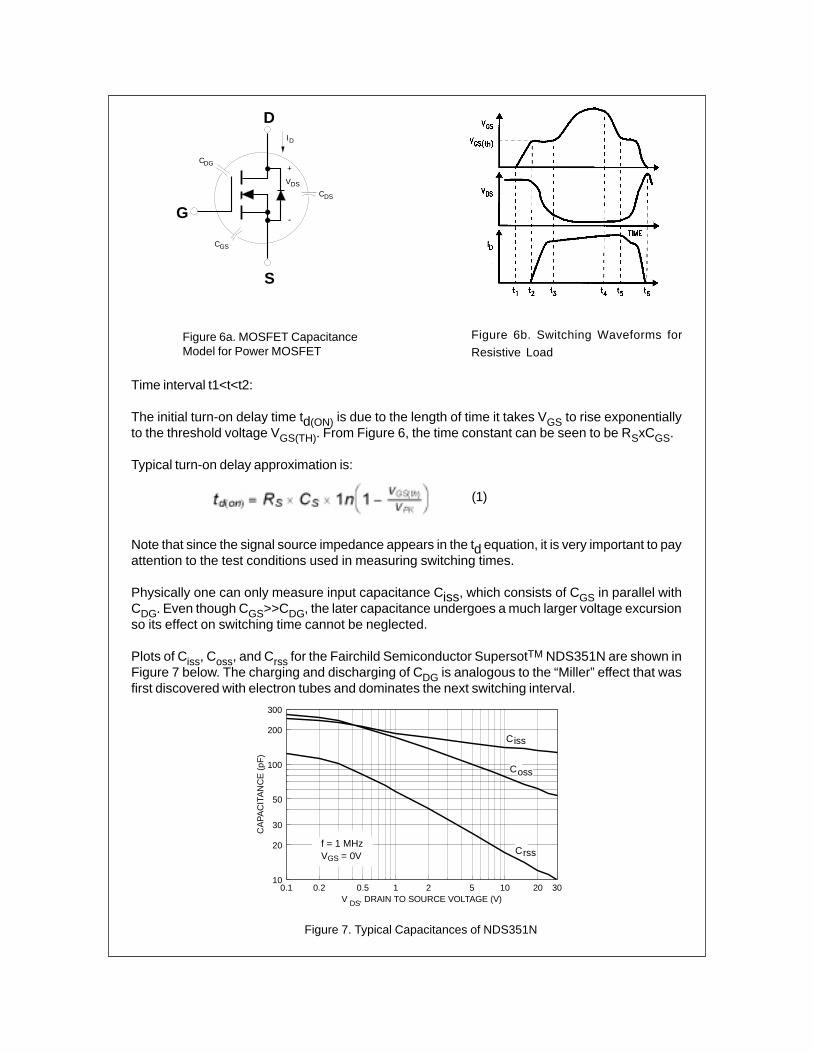
Time interval t1<t<t2:
The initial turn-on delay time td(ON) is due to the length of time it takes VGS to rise exponentiallyto the threshold voltage VGS(TH). From Figure 6, the time constant can be seen to be RSxCGS.
Typical turn-on delay approximation is:
(1)
Note that since the signal source impedance appears in the td equation, it is very important to payattention to the test conditions used in measuring switching times.
Physically one can only measure input capacitance Ciss, which consists of CGS in parallel withCDG. Even though CGS>>CDG, the later capacitance undergoes a much larger voltage excursionso its effect on switching time cannot be neglected.
Plots of Ciss, Coss, and Crss for the Fairchild Semiconductor SupersotTM NDS351N are shown inFigure 7 below. The charging and discharging of CDG is analogous to the “Miller” effect that wasfirst discovered with electron tubes and dominates the next switching interval.
S
D
G
DGC
GSC
DSCDSV
DI
+
-
Figure 6a. MOSFET CapacitanceModel for Power MOSFET
Figure 6b. Switching Waveforms for
Resistive Load
0.1 0.2 0.5 1 2 5 10 20 3010
20
30
50
100
200
300
V , DRAIN TO SOURCE VOLTAGE (V)
CA
PA
CIT
AN
CE
(pF
)
DS
C iss
f = 1 MHzV = 0VGS
C oss
C rss
Figure 7. Typical Capacitances of NDS351N

Time interval t2<t<t3:
Since VGS has now achieved the threshold value, the MOSFET begins to draw increasing loadcurrent and VDS decreases. CDG must not only discharge but its capacitance value also increasessince it is inversely proportional to VDS, namely:
(2)
Unless the gate driver can quickly supply the current required to discharged CDG, voltage fall willbe slowed with increases in turn-on time.
Time interval t3<t<t4:
The MOSFET is now on so the gate voltage can rise to the overdrive level.
Turn-off interval t4<t<t6:
Turn-off occurs in reverse order. VGS must drop back close to the threshold value before RDS(on)will start to increase. As VDS starts to rise, the Miller effect due to CDG re-occurs and impedes therise of VDS as CDG recharges to VCC.
Specific gate drive circuits for different applications are discussed and illustrated later in thispaper.
MOSFET CHARACTERIZATION
The output characteristics (ID vs VDS) of the Fairchild Semiconductor SupersotTM NDS351N areillustrated in Figures 8 and 9. The two distinct regions of operation in Figure 8 have been labeled“linear” and “saturated”. To understand the difference, recall that the actual current path in aMOSFET is horizontal through the channel created under the gate oxide and then vertical throughthe drain. In the linear region of operation, the voltage across the MOSFET channel is notsufficient for the carriers to reach their maximum current density. The static RDS(on), definedsimply as VDS/IDS, is a constant.
As VDS is increased, the carriers reach their maximum drift velocity and the current amplitudecannot increase. Since the device is behaving like a current generator, it is said to have high outputimpedance. This is the so-called “saturation” regions. One should also note that in comparingMOSFET operation to Bipolar transistor, the linear and saturated regions are just the opposite tothe MOSFET. The equal spacing between the output ID curves for constant step in VGS indicatesthat the transfer characteristics in Figure 9 will be linear in the saturated region.
Figure 8. NDS351N Output Characteristics Figure 9. NDS351N Transfer Characteristics

IMPORTANCE OF THRESHOLD VOLTAGE
Threshold voltage VGS(th) is the minimum gate voltage that initiates drain current flow. VGS(th) canbe easily measured on a Tektronix 576 curve tracer by connecting the gate to the drain andrecording the required drain voltage for a specified drain current, typically 250µA. VGS(th) in Figure9 is 1.6V. While a high value of VGS(th), can apparently lengthen turn-on delay time, a low value forPower MOSFET is undesirable for the following reasons:
1. VGS(th) decreases with increased temperature.2. The high gate impedance of a MOSFET makes it susceptible to spurious turn-on due to gatenoise.3. One of the more common modes of failure is gate-oxide voltage punch-through. Low VGS(th)requires thinner oxides, which lowers the gate oxide voltage rating.
POWER MOSFET THERMAL MODEL
Like all other power semiconductor devices, MOSFETs operate at elevated junction temperature.It is important to observe their thermal limitations in order to achieve acceptable performance andreliability. Specification sheets contain information on maximum junction temperature (TJ(max)),safe operating areas, current ratings and electrical characteristics as a function of TJ where appro-priate. However, since it is still not possible to cover all contingencies, it is still important that thedesigner perform some junction calculations to ensure that the device operates within specifica-tions.
Figure 10 shows an elementary, steady-state, thermal model for any power semiconductor andthe electrical analogue. The heat generated at the junction flows through the silicon pellet tothe case or tab and then to the heat sink. The junction temperature rise above the surroundingenvironment is directly proportional to this heat flow and the junction-to-ambient thermal resis-tance. The following equation defined the steady-state thermal resistance RθJA between devicejunction to ambient:
(3)where:TJ = average temperature at the device junction (oC)TA = average temperature at ambient (oC)P = average heat flow in watts (W).Note that for thermal resistance to be meaningful, two temperature reference points must bespecified. Units for RθJA are 0C/W.
Figure10. MOSFET Steady-State Thermal Resistance Model

The thermal model shows symbolically the locations for the reference points of junction tempera-ture, case temperature, sink temperature and ambient temperature. These temperature referencedefine the following thermal resistances:
RθJC: Junction-to-Case thermal resistance.RθCS: Case-to-Sink thermal resistance.RθSA:Sink-to-Ambient thermal resistance.
Since the thermal resistances are in series:
(4)
The design and manufacture of the device determines RθJC so that while RθJC will vary somewhatfrom device to device, it is the SOLE RESPONSIBILITY of the manufacturer to guarantee a maxi-mum value for RθJC. Both the user and manufacturer must cooperate in keeping RθCS to anacceptable maximum. Finally, the user has sole responsibility for the external heat sinking.By inspection of Figure 10, one can write an expression for TJ:
(5)
While this appears to be a very simple formula, the major problem using it is due to the fact thatthe power dissipated by the MOSFET depends upon TJ. Consequently one must use either aniterative or graphical solution to find the maximum RθSA to ensure stability. But an explanation oftransient thermal resistance is in order to handle the case of pulsed applications.
Use of steady-state thermal resistance is not satisfactory for finding peak junction temperaturesfor pulsed applications. Plugging in the peak power value results in overestimating the actualjunction temperature while using the average power value underestimates the peak junction tem-perature at the end of the power pulse. The reason for the discrepancy lies in the thermal capacityof the semiconductor and its housing, i.e., its ability to store heat and to cool down before the nextpulse.
The modified thermal model for the MOSFET is shown in Figure 11. The normally distributedthermal capacitances have been lumped into single capacitors labeled CJ, CC, and CS. Thissimplification assumes current is evenly distributed across the silicon chip and that the onlysignificant power losses occur in the junction. When a step pulse of heating power, P, is intro-duced at the junction, figure 12a shows that TJ will rise at an exponential rate to some steadystate value dependent upon the response of the thermal network. When the power input is termi-nated at time t2, TJ will decrease along the curve indicated by Tcool in Figure 12a back to its initialvalue. Transient thermal resistance at time t is thus defined as:
(6)
The transient thermal resistance curve approaches the steady-state value at long times and theslope of the curve for short times is inversely proportional to CJ. In order to use this curve
Figure 11. Transient Thermal Resistance Model

Figure 13c. Junction Temperature Response
to Individual Power PulseFigure 13d. Use of Superposition to Determine
Peak TJ
with confidence, it must represent the highest values ZθJC for each time interval that can beexpected from the manufacturing distribution of the products.
While predicting TJ in response to a series of power pulses becomes very complex, superpositionof power pulses offers a rigorous numerical method of using the transient thermal resistance curveto secure a solution. Superposition tests the response of a network to any input function byreplacing the input with an equivalent series of superimposed positive and negative step functions.Each step function must start from zero and continue to the time for which TJ is to be computed.For example, Figure 13 illustrates a typical train of heating pulses.
TJ at time is given by:
(7)
The typical use condition is to compute the peak junction temperature at thermal equilibrium for atrain of equal amplitude power pulses as shown in Figure 14.
Figure 12a. Junction Temperature Response to a
Step Pulse of Heating Power
Figure 12b. Transient Thermal Resistance Curve
for NDS351N
Figure 13a. Heat Input Figure 13b. Equivalent Heat Input by
Superposition of Power Pulses

To further simplify this calculation, the bracketed expression in equation (G) has been plotted forall Fairchild Semiconductor Power MOSFETs, as exemplified by the plot of ZθJC in Figure 14b.From this curve, one can readily calculate TJ if one knows PM. ZθJC and TC using the expression:
(8)
Example: Compute the maximum junction temperature for a train of 1W, 10ms wide heatingpulses repeated every 100ms. Assume a case temperature of 55oC.Duty factor=0.1From Figure 14b: ZθJC=0.14*250oC/W=35oC/WSubstituting into Equation (7):TJ(max)=55+1*35=90oC
SAFE OPERATING AREA
The Power MOSFET is not subjected to forward or reverse bias second breakdown, which caneasily occur in transistors. Second breakdown is a potentially catastrophic condition in transis-tors caused by thermal hot spots in the silicon as the transistor turns on or off. However in theMOSFET, the carriers travel through the device much as if it were a bulk semiconductor, whichexhibits positive temperature coefficient. If current attempts to self-constrict to a localized area,the increasing temperature of the spot will raise the spot resistance due to positive temperaturecoefficient of the bulk silicon. The ensuing higher voltage drop will tend to redistribute the currentaway from the hot spot. Figure 15 shows the safe operating area of the Fairchild SemiconductorSupersotTM NDS351N device.
Figure 14a. Train of Power Pulses Figure 14b. Normalized r(t) for NDS351N
Figure 15. Safe Operating Area of NDS351N

Note that the safe area boundaries are only thermally limited and exhibit no derating for secondbreakdown. This shows that while the MOSFET transistor is very rugged, it may still be destroyedthermally by forcing it to dissipate too much power.
ON-RESISTANCE RDS(on)
The on-resistance of a Power MOSFET is a very important parameter because it determines howmuch current the device can carry for low to medium frequency (less than 200kHz) applications.After being turned on, the on-state is defined simply as its on-state voltage divided by on-statecurrent. When conducting current as a switch, the conduction losses P are:
(9)
To minimize RDS(on), the applied gate signal should be large enough to maintain operation in thelinear or ohmic region as shown in Figure 8. Fairchild Semiconductor SUPERSOTTM-3 NDS351Nwill conduct its rated current for VGS=4.5V, which is also the value used to generate the curves ofRDS(on) vs ID and TJ that are shown in Figure 16 for the Fairchild Semiconductor Supersot NDS351N.Since RDS(on) is a function of TJ, Figure 16 plots this parameter at varies junction temperatures.Note that as the drain current rises, RDS(on) increases once ID exceeds the rated current value.Because the MOSFET is a majority carrier device, the component of RDS(on) due to the bulkresistance of the N- silicon in the drain region increases with temperature as well. While this mustbe taken into account to avoid thermal runaway, it does facilitate parallel operation of MOSFETs.Any imbalance between MOSFETs does not result in current hogging because the device with themost current heat up and ensuing higher on-voltage will divert some current to the other devices inparallel.
TRANSCONDUCTANCE
Since MOSFETs are voltage controlled, it has become necessary to resurrect the termtransconductance gFS, commonly used in the past with electron tubes. Referring to Figure 8, gFSequals to the change in drain current divided by the change in gate voltage for a constant drainvoltage. Mathematically:
(10)
Figure 16. RDS(on) of NDS351N

Transconductance varies with operating conditions, starting at 0 for VGS<VGS(th) and peaking at afinite value when the device is fully saturated. It is very small in the ohmic region because thedevice cannot conduct any more current. Transconductance is useful in designing linear amplifiersand does not have any significance in switching power supplies.
GATE DRIVE CIRCUITS FOR POWER MOSFETs
The drive circuit for a Power MOSFET will affect its switching behavior and its power dissipation.Consequently the type of drive circuitry depends upon the application. If on-state power lossesdue to RDS(on), will predominate, there is little point in designing a costly drive circuit. This powerdissipation is relatively independent of gate drive as long as the gate-source voltage exceeds thethreshold voltage by several volts and an elaborate drive circuit to decrease switching times willonly create additional EMI and voltage ringing. In contrast, the drive circuit for a device switching at200KHz or more will affect the power dissipation since switching losses are a significant part ofthe total power dissipation.
Compare to a junction transistor, the switching losses in a MOSFET can be made much smallerbut these losses must still be taken into consideration. Examples of several typical loads alongwith the idealized switching waveforms and expressions for power dissipation are given in Figure17 to 19.
Their power losses can be calculated from the general expression:
(11)
where fS =Switching frequency.
For the idealized waveforms shown in the figures, the integration can be approximated by thecalculating areas of triangles:Resistive loads:
Inductive Load:
Figure17. Resistive Load
Switching Waveforms
Figure18. Clamped Inductive
Load Switching WaveformsFigure19. Capacitive Load
Switching Waveforms
where PC = conduction loss during period T.

Capacitive load:
Gate losses and blocking losses can usually be neglected. Using these equations, circuit de-signer is able to estimate the required heat sink. A final heat run in a controlled temperatureenvironment is necessary to ensure thermal stability.
Since a MOSFET is essentially voltage controlled, the only gate current required is that neces-sary to charge the input capacitance Ciss. In contrast to a 10A transistor, which may require abase current of 2A to ensure saturation, a Power MOSFET can be driven directly by CMOS oropen-collector TTL logic circuit similar to that in Figure 20.
Turn-on speed depends upon the selection of resistor R1, whose minimum value will be deter-mined by the current sinking rating of the IC. It is essential that an open collector TTL buffer beused since the voltage applied to the gate must exceed the MOSFET threshold voltage. CMOSdevices can be used to drive the power device directly since they are capable of operating 15Vsupplies.
Interface ICs, originally intended for other applications, can be used to drive the Power MOSFETs,as shown below in Figure 21.
Figure 20. Open Collector TTL Drive Circuit
Figure 21. Interface ICs Used to Drive Power MOSFETs
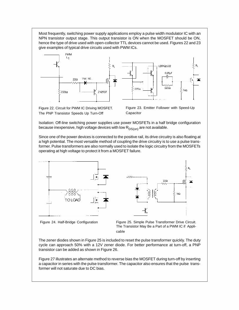
Most frequently, switching power supply applications employ a pulse width modulator IC with anNPN transistor output stage. This output transistor is ON when the MOSFET should be ON,hence the type of drive used with open-collector TTL devices cannot be used. Figures 22 and 23give examples of typical drive circuits used with PWM ICs.
Isolation: Off-line switching power supplies use power MOSFETs in a half bridge configurationbecause inexpensive, high voltage devices with low RDS(on) are not available.
Since one of the power devices is connected to the positive rail, its drive circuitry is also floating ata high potential. The most versatile method of coupling the drive circuitry is to use a pulse trans-former. Pulse transformers are also normally used to isolate the logic circuitry from the MOSFETsoperating at high voltage to protect it from a MOSFET failure.
The zener diodes shown in Figure 25 is included to reset the pulse transformer quickly. The dutycycle can approach 50% with a 12V zener diode. For better performance at turn-off, a PNPtransistor can be added as shown in Figure 26.
Figure 27 illustrates an alternate method to reverse bias the MOSFET during turn-off by insertinga capacitor in series with the pulse transformer. The capacitor also ensures that the pulse trans-former will not saturate due to DC bias.
Figure 22. Circuit for PWM IC Driving MOSFET.
The PNP Transistor Speeds Up Turn-Off
Figure 23. Emitter Follower with Speed-Up
Capacitor
Figure 24. Half-Bridge Configuration Figure 25. Simple Pulse Transformer Drive Circuit.The Transistor May Be a Part of a PWM IC if Appli-
cable

Opto-isolators may also be used to drive power MOSFETs but their long switching times makethem suitable only for low frequency applications.
SELECTING A DRIVE CIRCUIT
Any of the circuits shown are capable of turning a Power MOSFET on and off. The type of circuitdepends upon the application. The current sinking and sourcing capabilities of the drive circuit willdetermine the switching time and switching losses of the power device. As a rule, the higher thegate current at turn-on and turn-off, the lower the switching losses will be. However, fast drivecircuits may produce ringing in the gate circuit and drain circuits. At turn-on, ringing in the gatecircuit may produce a voltage transient in excess of the maximum VGS rating, which will puncturethe gate oxide and destroy it. To prevent this occurrence, a zener diode of appropriate value maybe added to the circuit as shown in Figure 28. Note that the zener should be mounted as close aspossible to the device.
At turn-off, the gate voltage may ring back up to the threshold voltage and turn on the device for ashort period. There is also the possibility that the drain-source voltage will exceed itsmaximum rated voltage due to ringing in the drain circuit. A protective RC snubber circuit or zenerdiode may be added to limit drain voltage to a safe level.
Figure 26. Improved Performance at Turn-Off
with a TransistorFigure 27. Emitter Follower Driver with Speed-
Up Capacitor
Figure 28. Zener Diode to Prevent Excessive Gate-Source Voltages

TRADEMARKS
ACEx™CoolFET™CROSSVOLT™E2CMOSTM
FACT™FACT Quiet Series™FAST®
FASTr™GTO™HiSeC™
The following are registered and unregistered trademarks Fairchild Semiconductor owns or is authorized to use and isnot intended to be an exhaustive list of all such trademarks.
LIFE SUPPORT POLICY
FAIRCHILD’S PRODUCTS ARE NOT AUTHORIZED FOR USE AS CRITICAL COMPONENTS IN LIFE SUPPORTDEVICES OR SYSTEMS WITHOUT THE EXPRESS WRITTEN APPROVAL OF FAIRCHILD SEMICONDUCTOR CORPORATION.As used herein:
ISOPLANAR™MICROWIRE™POP™PowerTrench™QS™Quiet Series™SuperSOT™-3SuperSOT™-6SuperSOT™-8TinyLogic™
1. Life support devices or systems are devices orsystems which, (a) are intended for surgical implant intothe body, or (b) support or sustain life, or (c) whosefailure to perform when properly used in accordancewith instructions for use provided in the labeling, can bereasonably expected to result in significant injury to theuser.
2. A critical component is any component of a lifesupport device or system whose failure to perform canbe reasonably expected to cause the failure of the lifesupport device or system, or to affect its safety oreffectiveness.
PRODUCT STATUS DEFINITIONS
Definition of Terms
Datasheet Identification Product Status Definition
Advance Information
Preliminary
No Identification Needed
Obsolete
This datasheet contains the design specifications forproduct development. Specifications may change inany manner without notice.
This datasheet contains preliminary data, andsupplementary data will be published at a later date.Fairchild Semiconductor reserves the right to makechanges at any time without notice in order to improvedesign.
This datasheet contains final specifications. FairchildSemiconductor reserves the right to make changes atany time without notice in order to improve design.
This datasheet contains specifications on a productthat has been discontinued by Fairchild semiconductor.The datasheet is printed for reference information only.
Formative orIn Design
First Production
Full Production
Not In Production
DISCLAIMER
FAIRCHILD SEMICONDUCTOR RESERVES THE RIGHT TO MAKE CHANGES WITHOUT FURTHERNOTICE TO ANY PRODUCTS HEREIN TO IMPROVE RELIABILITY, FUNCTION OR DESIGN. FAIRCHILDDOES NOT ASSUME ANY LIABILITY ARISING OUT OF THE APPLICATION OR USE OF ANY PRODUCTOR CIRCUIT DESCRIBED HEREIN; NEITHER DOES IT CONVEY ANY LICENSE UNDER ITS PATENTRIGHTS, NOR THE RIGHTS OF OTHERS.
©2001 Fairchild Semiconductor Corporation Application Note 7500 Rev. A
AN-7500
Understanding Power MOSFETs
Introduction
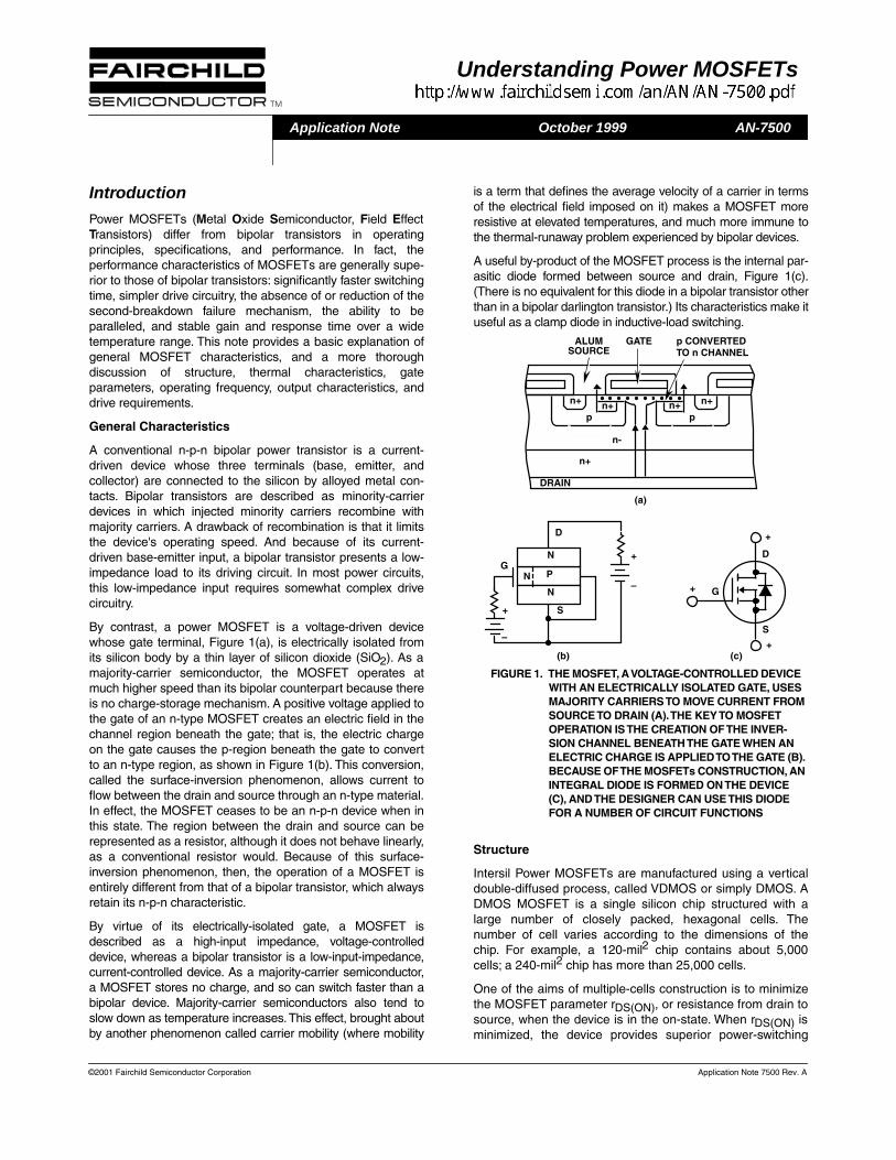
Power MOSFETs (Metal Oxide Semiconductor, Field EffectTransistors) differ from bipolar transistors in operatingprinciples, specifications, and performance. In fact, theperformance characteristics of MOSFETs are generally supe-rior to those of bipolar transistors: significantly faster switchingtime, simpler drive circuitry, the absence of or reduction of thesecond-breakdown failure mechanism, the ability to beparalleled, and stable gain and response time over a widetemperature range. This note provides a basic explanation ofgeneral MOSFET characteristics, and a more thoroughdiscussion of structure, thermal characteristics, gateparameters, operating frequency, output characteristics, anddrive requirements.
General Characteristics
A conventional n-p-n bipolar power transistor is a current-driven device whose three terminals (base, emitter, andcollector) are connected to the silicon by alloyed metal con-tacts. Bipolar transistors are described as minority-carrierdevices in which injected minority carriers recombine withmajority carriers. A drawback of recombination is that it limitsthe device's operating speed. And because of its current-driven base-emitter input, a bipolar transistor presents a low-impedance load to its driving circuit. In most power circuits,this low-impedance input requires somewhat complex drivecircuitry.
By contrast, a power MOSFET is a voltage-driven devicewhose gate terminal, Figure 1(a), is electrically isolated fromits silicon body by a thin layer of silicon dioxide (SiO2). As amajority-carrier semiconductor, the MOSFET operates atmuch higher speed than its bipolar counterpart because thereis no charge-storage mechanism. A positive voltage applied tothe gate of an n-type MOSFET creates an electric field in thechannel region beneath the gate; that is, the electric chargeon the gate causes the p-region beneath the gate to convertto an n-type region, as shown in Figure 1(b). This conversion,called the surface-inversion phenomenon, allows current toflow between the drain and source through an n-type material.In effect, the MOSFET ceases to be an n-p-n device when inthis state. The region between the drain and source can berepresented as a resistor, although it does not behave linearly,as a conventional resistor would. Because of this surface-inversion phenomenon, then, the operation of a MOSFET isentirely different from that of a bipolar transistor, which alwaysretain its n-p-n characteristic.
By virtue of its electrically-isolated gate, a MOSFET isdescribed as a high-input impedance, voltage-controlleddevice, whereas a bipolar transistor is a low-input-impedance,current-controlled device. As a majority-carrier semiconductor,a MOSFET stores no charge, and so can switch faster than abipolar device. Majority-carrier semiconductors also tend toslow down as temperature increases. This effect, brought aboutby another phenomenon called carrier mobility (where mobility
is a term that defines the average velocity of a carrier in termsof the electrical field imposed on it) makes a MOSFET moreresistive at elevated temperatures, and much more immune tothe thermal-runaway problem experienced by bipolar devices.
A useful by-product of the MOSFET process is the internal par-asitic diode formed between source and drain, Figure 1(c).(There is no equivalent for this diode in a bipolar transistor otherthan in a bipolar darlington transistor.) Its characteristics make ituseful as a clamp diode in inductive-load switching.
Structure
Intersil Power MOSFETs are manufactured using a verticaldouble-diffused process, called VDMOS or simply DMOS. ADMOS MOSFET is a single silicon chip structured with alarge number of closely packed, hexagonal cells. Thenumber of cell varies according to the dimensions of thechip. For example, a 120-mil2 chip contains about 5,000cells; a 240-mil2 chip has more than 25,000 cells.
One of the aims of multiple-cells construction is to minimizethe MOSFET parameter rDS(ON), or resistance from drain tosource, when the device is in the on-state. When rDS(ON) isminimized, the device provides superior power-switching
n+ n+
n-
pn+ n+
n+
DRAIN
ALUM GATE p CONVERTEDTO n CHANNEL
(a)
+ G
S
D
+
+(c)
p
D
N
P
N
GN
S+
–
+
–
(b)
FIGURE 1. THE MOSFET, A VOLTAGE-CONTROLLED DEVICE WITH AN ELECTRICALLY ISOLATED GATE, USES MAJORITY CARRIERS TO MOVE CURRENT FROM SOURCE TO DRAIN (A). THE KEY TO MOSFET OPERATION IS THE CREATION OF THE INVER-SION CHANNEL BENEATH THE GATE WHEN AN ELECTRIC CHARGE IS APPLIED TO THE GATE (B). BECAUSE OF THE MOSFETs CONSTRUCTION, AN INTEGRAL DIODE IS FORMED ON THE DEVICE (C), AND THE DESIGNER CAN USE THIS DIODE FOR A NUMBER OF CIRCUIT FUNCTIONS
SOURCE
Application Note October 1999
[ /Title (AN7244)/Sub-ject (Understand-ing Power MOS-FETs, Inter-sil Corpo-ration)/Author ()/Key-words ()/Cre-ator ()/DOCINFO pdf-mark
[ /Page-Mode /Use-Out-lines/DOC-VIEW pdf-mark
John P Taylor
http://www.fairchildsemi.com/an/AN/AN-7500.pdf

©2001 Fairchild Semiconductor Corporation Application Note 7500 Rev. A
performance because the voltage drop from drain to sourceis also minimized for a given value of drain-to-source current.
Since the path between drain and source is essentiallyresistive, because of the surface-inversion phenomenon,each cell in the device can be assumed to contribute anamount, RN, to the total resistance. An individual cell has afairly low resistance, but to minimize rDS(ON), it is necessaryto put a large number of cells in parallel on a chip. In general,therefore, the greater the number of paralleled cells on achip, the lower its rDS(ON) value:
rDS(ON) = RN/N, where N is the number of cells.
In reality, rDS(ON) is composed of three separate resis-tances. Figure 2 shows a curve of the three resistive compo-nents for a single cell and their contributions to the overallvalue of rDS(ON). The value of rDS(ON) at any point of thecurve is found by adding the values of the three componentsat that point:
rDS(ON) = RBULK + RCHAN + REXT
where RCHAN represents the resistance of the channelbeneath the gate, and REXT includes all resistances resultingfrom the substrate, solder connections, leads, and thepackage. RBULK represents the resistance resulting from thenarrow neck of n material between the two layers, as shown inFigure 1(a), plus the resistance of the current path below theneck and through the body to the substrate region of thedevice.
Note in Figure 2 that RCHAN and REXT are completely inde-pendent of voltage, while RBULK is highly dependent onapplied voltage. Note also that below about 150 volts,rDS(ON) is dominated by the sum of RCHAN and REXT.Above 150 volts, rDS(ON) is increasingly dominated byRBULK. Table 1 gives a percentage breakdown of the contri-bution of each resistance for three values of voltage.
Two conclusions, inherent consequences of the laws ofsemiconductor physics, and valid for any DMOS device, canbe drawn from the preceding discussion: First, rDS(ON)obviously increases with increasing breakdown-voltagecapability of a MOSFET. Second, minimum rDS(ON)performance must be sacrificed if the MOSFET must with-stand ever-higher breakdown voltages.
The significance of RBULK in devices with a high voltagecapability is due to the fact that thick, lightly doped epi layersare required for the drain region in order to avoid producinghigh electric fields (and premature breakdown) within thedevice. And as the epi layers are made thicker and lessresistive to support high voltages, the bulk component ofresistance rapidly increases (see Figure 2) and begins todominate the channel and external resistance. The rDS(ON)therefore, increases with increasing breakdown voltagecapability, and low rDS(ON) must be sacrificed if theMOSFET is to withstand even higher breakdown voltages.
There is a way around these obstacles. The rDS(ON) in Fig-ure 2 holds only for a given cell and chip size. Using a largerchip results in a lower value for rDS(ON) because a large chiphas more cells (see Figure 3), shifting the vertical axis foreach of the constituent parts.
The penalty for using a larger chip, however, is an increasein cost, since chip size is a major cost factor. And becausechip area increases exponentially, not linearly, with voltage,the additional cost can be substantial. For example, to obtaina given rDS(ON) at a breakdown voltage twice as great as theoriginal, the new chip requires an area four or five timeslarger than the original. Although the cost does not riseexponentially, it is substantially more than the original cost.
Effects of Temperature
The high operating temperatures of bipolar transistors arefrequent cause of failure. The high temperatures are causedby hot-spotting, the tendency of current in a bipolar device toconcentrate in areas around the emitter. Unchecked, thishot-spotting results in the mechanism of thermal runaway,and eventual destruction of the device. MOSFETs do notsuffer this disadvantage because their current flow is in theform of majority carriers. The mobility of majority carriers(where, again, mobility is a term that defines the averagevelocity of a carrier in terms of the electrical field imposed onit) is temperature dependent in silicon: mobility decreaseswith increasing temperature. This inverse relationshipdictates that the carriers slowdown as the chip gets hotter. Ineffect, the resistance of the silicon path is increased, whichprevents the concentrations of current that lead to hot spots.In fact, if hot spots do attempt to form in a MOSFET, the localresistance increases and defocuses or spreads out thecurrent, rerouting it to cooler portions of the chip.
TABLE 1. PERCENTAGE RESISTANCE COMPONENTS FOR A TYPICAL CHIP
BVDSS 40V 150V 500V
RCHANNEL 50% 23% 2.4%
RBULK 35% 70% 97%
REXTERNAL 15% 7% <1%
100 100030
3000
1000
100
10
REXT
RCHAN
RBULK
rDS(ON)
BVDSS (V)
r DS
(ON
) (m
Ω)
REXT
RCHANRBULK
rDS(ON)
FIGURE 2. THE DRAIN-TO-SOURCE RESISTANCE, rDS(ON), OF A MOSFET IS NOT ONE BUT THREE SEPARATE RESISTANCE COMPONENTS
Application Note 7500

©2001 Fairchild Semiconductor Corporation Application Note 7500 Rev. A
Because of the character of its silicon structure, a MOSFET has a positive temperature coefficient of resistance, as shown by the curves of Figure 4.
The positive temperature coefficient of resistance meansthat a MOSFET is inherently more stable with temperaturefluctuation, and provides its own protection against thermalrunaway and second breakdown. Another benefit of thischaracteristic is that MOSFETs can be operated in parallelwithout fear that one device will rob current from the others.If any device begins to overheat, its resistance will increase,and its current will be directed away to cooler chips.
Gate Parameters
To permit the flow of drain-to-source current in an n-typeMOSFET, a positive voltage must be applied between thegate and source terminals. Since, as described above, thegate is electrically isolated from the body of the device,theoretically no current can flow from the driving source intothe gate. In reality, however, a very small current, in the
range of tens of nanoamperes, does flow, and is identified ondata sheets as a leakage current, IGSS. Because the gatecurrent is so small, the input impedance of a MOSFET isextremely high (in the megohm range) and, in fact, is largelycapacitive rather than resistive (because of the isolation ofthe gate terminal).
Figure 5 illustrates the basic input circuit of a MOSFET. The ele-ments are equivalent, rather than physical, resistance, R, andcapacitance, C. The capacitance, called CISS on MOSFET datasheets, is a combination of the device's internal gate-to-sourceand gate-to-drain capacitance. The resistance, R, representsthe resistance of the material in the gate circuit. Together, theequivalent R and C of the input circuit will determine the upperfrequency limit of MOSFET operation.
Operating Frequency
Most DMOS processes use a polysilicon gate structurerather than the metal-gate type. If the resistance of the gatestructure (R in Figure 5) is high, the switching time of theDMOS device is increased, thereby reducing its upper oper-ating frequency. Compared to a metal gate, a polysilicongate has a higher gate resistance. This property accounts forthe frequent use of metal-gate MOSFETs in high-frequency(greater than 20MHz) applications, and polysilicon-gateMOSFETs in higher-power but lower-frequency systems.
Since the frequency response of a MOSFET is controlled bythe effective R and C of its gate terminal, a rough estimatecan be made of the upper operating frequency fromdatasheet parameters. The resistive portion depends on thesheet resistance of the polysilicon-gate overlay structure, avalue of approximately 20 ohms. But whereas the total Rvalue is not found on datasheets, the C value (CISS) is; it isrecorded as both a maximum value and in graphical form asa function of drain-to-source voltage. The value of CISS isclosely related to chip size; the larger the chip, the greaterthe value. Since the RC combination of the input circuit mustbe charged and discharged by the driving circuit, and sincethe capacitance dominates, larger chips will have slowerswitching times than smaller chips, and are, therefore, moreuseful in lower-frequency circuits. In general, the upperfrequency limit of most power MOSFETs spans a fairly broadrange, from 1MHz to 10MHz.
0 100 200 300 400 500 600
BVDSS (V)
10642
1
0.60.4
0.2
0.1
0.060.04
0.02
0.01
r DS
(ON
) (Ω
)
CHIP
CHIP
LARGEST
SMALLEST
FIGURE 3. AS CHIP SIZE INCREASES, rDS(ON) DECREASES
ID = 4AVGS = 10V
4
3
2
1
0-50 0 50 100 150 200
JUNCTION TEMPERATURE - TJ (oC)
r DS
(ON
) (Ω
)
FIGURE 4. MOSFETs HAVE A POSITIVE TEMPERATURE COEFFICIENT OF RESISTANCE, WHICH GREATLY REDUCES THE POSSIBILITY OF THERMAL RUNAWAY AS TEMPERATURE INCREASES
GS
D
CISS
R
FIGURE 5. A MOSFETs SWITCHING SPEED IS DETERMINED BY ITS INPUT RESISTANCE R AND ITS INPUT CAPACITANCE CISS
Application Note 7500

©2001 Fairchild Semiconductor Corporation Application Note 7500 Rev. A
Output Characteristics
Probably the most used MOSFET graphical data is theoutput characteristics or a plot of drain-to-source current(IDS) as a function of drain-to-source voltage (VDS). A typi-cal characteristic, shown in Figure 6, gives the drain currentthat flows at various VDS values as a function of the gate-to-source voltage (Vgs). The curve is divided into tworegions: a linear region in which VDS is small and drain cur-rent increases linearly with drain voltage, and a saturatedregion in which increasing drain voltage has no effect ondrain current (the device acts as a constant-current source).The current level at which the linear portion of the curve joinswith the saturated portion is called the pinch-off region.
Drive Requirements
When considering the Vgs level required to operate aMOSFET, note from Figure 6, that the device is not turnedon (no drain current flows) unless Vgs is greater than acertain level (called the threshold voltage). In other words,the threshold voltage must be exceeded before an apprecia-ble increase in drain current can be expected. Generally Vgsfor many types of DMOS devices is at least 2V. This is animportant consideration when selecting devices or designingcircuits to drive a MOSFET gate: the gate-drive circuit mustprovide at least the threshold-voltage level, but preferably, amuch higher one.
As Figure 6 shows, a MOSFET must be driven by a fairlyhigh voltage, on the order of 10V, to ensure maximumsaturated drain-current flow. However, integrated circuits,such as TTL types, cannot deliver the necessary voltagelevels unless they are modified with external pull-upresistors. Even with a pull-up to 5V, a TTL driver cannot fullysaturate most MOSFETs. Thus, TTL drivers are mostsuitable when the current to be switched is far less than therated current of the MOSFET. CMOS ICs can run fromsupplies of 10V, and these devices are capable of driving aMOSFET into full saturation. On the other hand, a CMOSdriver will not switch the MOSFET gate circuit as fast as aTTL driver. The best results, whether TTL or CMOS ICsprovide the drive, are achieved when special buffering chipsare inserted between the IC output and gate input to matchthe needs of the MOSFET gate.
PULSE TESTPULSE DURATION = 80µSDUTY CYCLE ≤ 2%TC = 25oC
VG = 8V
VG = 7V
VG = 6V
VG = 5V
VG = 4V
VG = 10V
VG = 20V
0 2 4 6 8 10 12 14
DRAIN-TO-SOURCE VOLTAGE - VDS (V)
DR
AIN
CU
RR
EN
T -
I D (
A)
30
25
20
15
10
5
0
FIGURE 6. MOSFETs REQUIRE A HIGH INPUT VOLTAGE (AT LEAST 10V) IN ORDER TO DELIVER THEIR FULL RATED DRAIN CURRENT
Application Note 7500

TRADEMARKS
The following are registered and unregistered trademarks Fairchild Semiconductor owns or is authorized to use and isnot intended to be an exhaustive list of all such trademarks.
LIFE SUPPORT POLICY
FAIRCHILD’S PRODUCTS ARE NOT AUTHORIZED FOR USE AS CRITICAL COMPONENTS IN LIFE SUPPORTDEVICES OR SYSTEMS WITHOUT THE EXPRESS WRITTEN APPROVAL OF FAIRCHILD SEMICONDUCTOR CORPORATION.As used herein:1. Life support devices or systems are devices orsystems which, (a) are intended for surgical implant intothe body, or (b) support or sustain life, or (c) whosefailure to perform when properly used in accordancewith instructions for use provided in the labeling, can bereasonably expected to result in significant injury to theuser.
2. A critical component is any component of a lifesupport device or system whose failure to perform canbe reasonably expected to cause the failure of the lifesupport device or system, or to affect its safety or
effectiveness.
PRODUCT STATUS DEFINITIONS
Definition of Terms
Datasheet Identification Product Status Definition
Advance Information
Preliminary
No Identification Needed
Obsolete
This datasheet contains the design specifications forproduct development. Specifications may change inany manner without notice.
This datasheet contains preliminary data, andsupplementary data will be published at a later date.Fairchild Semiconductor reserves the right to makechanges at any time without notice in order to improvedesign.
This datasheet contains final specifications. FairchildSemiconductor reserves the right to make changes atany time without notice in order to improve design.
This datasheet contains specifications on a productthat has been discontinued by Fairchild semiconductor.The datasheet is printed for reference information only.
Formative orIn Design
First Production
Full Production
Not In Production
DISCLAIMER
FAIRCHILD SEMICONDUCTOR RESERVES THE RIGHT TO MAKE CHANGES WITHOUT FURTHERNOTICE TO ANY PRODUCTS HEREIN TO IMPROVE RELIABILITY, FUNCTION OR DESIGN. FAIRCHILDDOES NOT ASSUME ANY LIABILITY ARISING OUT OF THE APPLICATION OR USE OF ANY PRODUCTOR CIRCUIT DESCRIBED HEREIN; NEITHER DOES IT CONVEY ANY LICENSE UNDER ITS PATENTRIGHTS, NOR THE RIGHTS OF OTHERS.
PACMAN™POP™PowerTrenchQFET™QS™QT Optoelectronics™Quiet Series™SILENT SWITCHERSMART START™Star* Power™Stealth™
FASTFASTr™GlobalOptoisolator™GTO™HiSeC™ISOPLANAR™LittleFET™MicroFET™MICROWIRE™OPTOLOGIC™OPTOPLANAR™
Rev. H
ACEx™Bottomless™CoolFET™CROSSVOLT™DenseTrench™DOME™EcoSPARK™E2CMOSTM
EnSignaTM
FACT™FACT Quiet Series™
SuperSOT™-3SuperSOT™-6SuperSOT™-8SyncFET™TinyLogic™UHC™UltraFET™VCX™

AN-936 (v.Int)
The Do's and Don'ts of Using MOS-Gated Transistors(HEXFET® is the trademark for International Rectifier Power MOSFETs)
In this application note, some of the most common do's and don'ts of using power HEXFET®s are described. The objective is tohelp the user get the most out of these remarkable devices, while reducing "on the job" learning time to a minimum.
Topics Covered:Be Mindful of the Reverse Blocking Characteristics of the DeviceBe Careful When Handling and Testing Power HEXFET®sBeware of Unexpected Gate-to-Source Voltage SpikesBeware of Drain or Collector Voltage Spikes Induced by SwitchingDo Not Exceed the Peak Current RatingStay within the Thermal Limits of the DevicePay Attention to Circuit LayoutBe Careful When Using the Integral Body-Drain DiodeBe On Your Gaurd When Comparing Current Ratings
1. BE MINDFUL OF THE REVERSE BLOCKING CHARACTERISTICS OFTHE DEVICE
IGBTs have a limited reverse blocking capability of approximately 20-30 V, with high leakage. This is characterized in IR’s datasheets with a Reverse Avalanche Energy (EARV). This rating isuseful to absorb energy spikes due to the stray inductance inseries with the anti-parallel diode. This is a significantadvantage over bipolar transistors and power darlingtons.A feature of power MOSFETs is that they inherently have builtinto them an integral reverse body-drain diode. The existence ofthis diode is explained by reference to Figure 1. When thesource terminal is made positive with respect to the drain,current can flow through the middle of the source cell, across aforward biased P-N junction. In the "reverse" direction, thepower HEXFET® thus behaves like a P-N junction rectifier. Theintegral body-drain diode is a real circuit element, and itscurrent handling capability is typically as high as that of thetransistor itself. Some circuits require an "inverse" rectifier to beconnected across the switching device, and in these circuits itwill often be possible to utilize the body-drain diode of theHEXFET® provided the proper precautions are taken.
2. BE CAREFUL WHEN HANDLING & TESTING POWER HEXFET®S
The user's first "contact" with a MOS-gated transistor could be a package of parts arriving on his desk. Even at this stage, itbehooves one to be knowledgeable about some elementary precautions. Being MOS devices, HEXFET®s can be damaged by staticcharge when handling, testing or installing into a circuit. Power Devices have large input capacitance, and are able to absorbstatic charge without excessive buildup of voltage. In order to avoid possible problems, however, the following procedures shouldbe followed as a matter of good practice, wherever possible:
• MOS-gated transistors should be left in their anti-static shipping bags, or conductive foam, or they should be placed in metalcontainers or conductive tote bins, until required for testing or connection into a circuit. The person handling the deviceshould ideally be grounded through a suitable wrist strap, though in reality this added precaution is seldom essential.
• Devices should be handled by the package, not by the leads. When checking the electrical characteristics of the MOS-gatedtransistors on a curve tracer, or in a test circuit, the following precautions should be observed:
• Test stations should use electrically conductive floor and table mats that are grounded. Suitable mats are availablecommercially.
Figure 1. Basic HEXFET Structure
John P Taylor
http://www.irf.com/technical-info/appnotes/an-936.pdf

AN-936 (v.Int)• When inserting the device in a curve tracer or a test circuit, voltage should not be applied until all terminals are solidly
connected into the circuit.• When using a curve tracer, a resistor should be connected in series with the gate to damp spurious oscillations that can
otherwise occur on the trace. A suitable value of resistance is 100 ohms.• For repeated testing, it is convenient to build this resistor into the test fixture.• When switching from one test range to another, voltage and current settings should be reduced to zero, to avoid the
generation of potentially destructive voltage surges during switching. The next step is to connect the device into an actual circuit. The following simple precautions should be observed: • Work stations should use electrically grounded table and floor mats.• Soldering irons should be grounded.
Now that the device has been connected into its circuit, it is ready for the power to be applied. From here on, success in applyingthe device becomes a matter of the integrity of the circuit design, and of what circuit precautions have been taken to guardagainst unintentional abuse of its ratings.
The following are the interrelated device and circuit considerations that lead to reliable, trouble-free design.
3. BEWARE OF UNEXPECTED GATE-TO-SOURCE VOLTAGE SPIKES
Excessive voltage will punch through the gate-source oxide layer and result in permanent damage. This seems obvious enough,but it is not so obvious that transient gate-to-source overvoltages can be generated that are quite unrelated to, and well in excessof, the amplitude of the applied drive signal. The problem is illustrated by reference to Figure 2.If we assume that the impedance, Z, of the drive source is high, then any positive-going change of voltage applied across thedrain and source terminals (caused, for example, by the switching of another device in the circuit) will be reflected as a positive-going voltage transient across the source and the drain terminals, in the approximate ratio of:
The above ratio is typically about 1 to 6. This means that a change of drain-to-source voltage of 300V, for example, couldproduce a voltage transient approaching 50V between the gate and source terminals. In practice this “aiming” voltage will notappear on the gate if the dv/dt is positive because the MOS-gated device goes in conduction at approximately Vgs = 4V, therebyclamping the dv/dt at the expense of a current transient and increased power dissipation. However, a negative-going dv/dt willnot be clamped. This calculation is based upon the worst case assumption that the transient impedance of the drive circuit is highby comparison with the gate-to-source capacitance of the device. This situation can, in fact, be quite easily approximated if thegate drive circuit contains inductance—for example the leakage inductance of an isolating drive transformer. This inductanceexhibits a high impedance for short transients, and effectively decouples the gate from its drive circuit for the duration of thetransient.
The negative-going gate-to-source voltage transient produced under the above circumstances may exceed the gate voltage ratingof the device, causing permanent damage. It is, of course, true that since the applied drain transient results in a voltage at thegate which tends to turn the device ON, the overall effect is to an extent self-limiting so far as the gate voltage transient isconcerned. Whether this self-limiting action will prevent the voltage transient at the gate from exceeding the gate-source voltagerating of the device depends upon the impedance of the external circuit. Spurious turn-on is of itself undesirable, of course,though in practical terms one may grudgingly be able to accept this circuit operating imperfection, provided the safe operatingarea of the device is not violated.
Notice that a voltage clamp (a conventional zener diode is suitable for this purpose) to prevent the gate-source voltage ratingfrom being exceeded will not prevent the dv/dt induced turn-on, as the gate will not reach the zener voltage. In many instancesthe zener is responsible for generating oscillations in the gate circuit, particularly when a significant amount of stray inductanceis present. A more fundamental solution, of course, is to make the impedance of the gate circuit low enough that not only is thegate-source voltage rating not exceeded, but also the voltage transient at the gate is contained to a level at which spurious turn-ondoes not occur.
1
1+C
C
gs
dg

AN-936 (v.Int)
It should be remembered that a collapse of voltage across the device (i.e., a negative-going dv/dt) will produce a transientnegative voltage spike across the gate-source terminals. In this case, of course, there will be no tendency for the device to turnON, and hence no tendency for the effect to be self-limiting. A zener diode connected to clamp positive transients willautomatically clamp negative-going transients, limiting them to the forward conduction voltage drop of the zener.
"POSITIVEGOING"CHANGE
"NEGATIVE GOING"CHANGE
DRAIN-SOURCEVOLTAGE
WITH NOCLAMPING GATE-SOURCE
VOLTAGE
WITH NOCLAMPING
D
CDS
CDG
CGS
S
ZG
DRIVESOURCE
IMPEDANCE
EXTERNALLY CONNECTEDCLAMPING ZENER DIODE
Figure 2. A Rapidly Changing Applied Drain-Source Voltage will Produce Gate-Source Transients
R
L
+E
(a) UNCLAMPEDINDUCTIVE
LOAD
OVERVOLTAGETRANSIENTDUE TO L
Figure 3. Drain-Source Overvoltage Transient whenSwitching Off with Unclamped Inductive Load
+E
LS
LS
R
L
LSD
S
VDS
E(b) CLAMPEDINDUCTIVE
LOAD
OVERVOLTAGETRANSIENTDUE TO LS
LS = STRAY CIRCUITINDUCTANCE
Figure 4. Drain-Source Overvoltage TransientProduced by Stray Circuit Inductance When Switching
Off with Clamped, Inductive Load

AN-936 (v.Int)
4. BEWARE OF DRAIN OR COLLECTOR VOLTAGE SPIKES INDUCED BYSWITCHING
The uninitiated designer is often not aware that self-inflicted overvoltage transients can be produced when the device is switchedOFF, even though the DC supply voltage for the drain circuit is well below the VDS rating of the transistor.Figure 3 shows how a voltage spike is produced when switching the device OFF, as a result of inductance in the circuit. Thefaster the device is switched, the higher the overvoltage will be.Inductance is always present to some extent in a practical circuit, and therefore, there is always danger of inducing overvoltagetransients when switching OFF. Usually, of course, the main inductive component of the load will be "clamped", as shown inFigure 4. Stray circuit inductance still exists, however, and overvoltage transients will still be produced as a result—to saynothing of the fact that the clamping diode may not provide an instantaneous clamping action, due to its "forward recovery"characteristic.
The first approach to this problem is to minimize stray circuit inductance, by means of careful attention to circuit layout, to thepoint that whatever residual inductance is left in the circuit can be tolerated. HEXFET®s have an inductive energy rating thatmakes capable of withstanding these inductive spikes, assuming that the data sheet limits for energy and temperature are notviolated. IGBTs, however, do not have an avalanche rating, and a clamping device should be connected, physically as close aspossible to the drain and source terminals, as shown in Figure 5. A conventional zener diode, or a "transorb" clamping device,are satisfactory for this purpose. An alternative clamping circuit is shown in Figure 6, depending on the voltage and currentrating of the circuit. The capacitor C is a reservoir capacitor and charges to a substantially constant voltage, while the resistor R is sized to dissipatethe "clamping energy" while maintaining the desired voltage across the capacitor. The diode D must be chosen so that its forwardrecovery characteristic does not significantly spoil the transient clamping action of the circuit. A simple RC snubber can also beused, as shown in Figure 7. Note, however, that an RC snubber not only limits the peak voltage, it also slows down the effectiveswitching speed. In so doing, it absorbs energy during the whole of the switching period, not just at the end of it, as does avoltage clamp. A snubber is therefore less efficient than a true voltage clamping device.
Note that the highest voltage transient occurs when switching the highest level of current. The waveform of the voltage across thedevice should be checked with a high-speed oscilloscope at the full load condition to ensure that switching voltage transients arewithin safe limits.
5. DO NOT EXCEED THE PEAKCURRENT RATING
All power transistors have a specified maximum peakcurrent rating. This is conservatively set at a level thatguarantees reliable operation and it should not beexceeded. It is often overlooked that, in a practicalcircuit, peak transient currents can be obtained that arewell in excess of the expected normal operating current,unless proper precautions are taken. Heating, lightingand motor loads, for example, consume high in-rushcurrents if not properly controlled. A technique thatensures that the peak current does not exceed thecapability of the device is to use a current sensing controlthat switches it OFF whenever the currentinstantaneously reaches a preset limit.
Unexpectedly high transient current can also be obtainedas a result of rectifier reverse recovery, when a transistoris switched ON rapidly into a conducting rectifier. This isillustrated in Figure 8. The solution is to use a fasterrectifier, or to slow down the switching of the transistorto limit the peak reverse recovery current of the rectifier.
6. STAY WITHIN THE THERMAL LIMITS
+E
LS
LSR
L
LSVDS
D
S CLAMPINGZENER
OVERVOLTAGETRANSIENTCLAMPEDBY ZENER
(c) CLAMPEDINDUCTIVE LOADWITH LOCAL D-SZENER CLAMP
Figure 5. Overvoltage Transient at Switch-Off Clamped byLocal Drain-Source Zener

AN-936 (v.Int)
Power transistors are thermally limited. They must bemounted on a heatsink that is adequate to keep thejunction temperature within the rated under the"worst case" condition of maximum power dissipationand maximum ambient temperature.
It must be remembered that in a switchingapplication, the total power is due to the conductionlosses and the switching loss. Switching time andswitching losses of HEXFET®s are essentiallyindependent of temperature, but the conduction lossesincrease with increasing temperature, because RDS(on)
increases with temperature. IGBTs, on the contrary,have switching losses that highly dependent oftemperature, while conduction losses are not. Thismust be taken into account when sizing the heatsink.The required thermal resistance of the heatsink canbe calculated as follows:The transistor conduction power, PT, is given
approximately by PT = On-state Voltage x Drain orCollector currentThe switching energy depends upon the voltage andcurrent being switched and the type of load. The totalswitching loss, PS, is the total switching energy, εT,
multiplied by the operating frequency, f. eT is the sumof the energies due to the individual switchings thattake place in each fundamental operating cycle:
PS = εT f
The total power dissipation is the sum of the conduction power, PT, and the switching power, PS.
P = PT + PS
Since:∆TJA = PRth
where:Rth = junction-to-ambient thermal
resistance
The junction-to-ambient thermal resistance, RJA,is made up of the internal junction-to-casethermal resistance, RJC, plus the case-to-
heatsink thermal resistance, RCS, plus the sink-
to-ambient thermal resistance, RSA. The firsttwo terms are fixed for the device, and therequired thermal resistance of the heatsink, RS-
A, for a given junction temperature rise DTJ-A,can be calculated from:
RS-A = RJ-A - (RJC + RC-S)
7. PAY ATTENTION TO CIRCUIT LAYOUT
+E
E
EC
D
R
C
EC
0
Figure 6. Overvoltage Transient at Switch-Off Limited byLocal Clamp
+ELS
LSR
L
LS
D
S
(d) CLAMPED INDUCTIVELOAD WITH LOCAL
D-S SNUBBER
VDS
SNUBBER
OVERVOLTAGE TRANSIENTREDUCED BY SNUBBER
E
Figure 7 . Overvoltage Transient at Switch-Off Limited by LocalCapacitor-Resistor Snubber
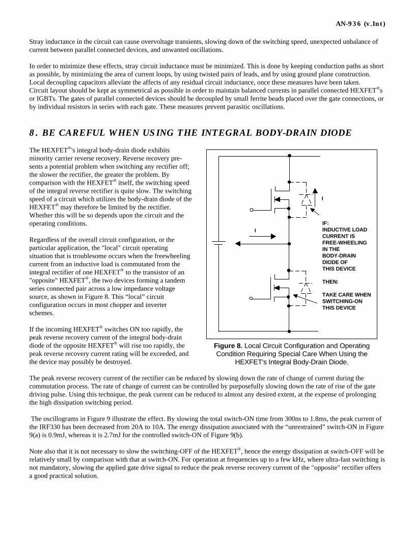
AN-936 (v.Int)
Stray inductance in the circuit can cause overvoltage transients, slowing down of the switching speed, unexpected unbalance ofcurrent between parallel connected devices, and unwanted oscillations.
In order to minimize these effects, stray circuit inductance must be minimized. This is done by keeping conduction paths as shortas possible, by minimizing the area of current loops, by using twisted pairs of leads, and by using ground plane construction.Local decoupling capacitors alleviate the affects of any residual circuit inductance, once these measures have been taken.Circuit layout should be kept as symmetrical as possible in order to maintain balanced currents in parallel connected HEXFET®sor IGBTs. The gates of parallel connected devices should be decoupled by small ferrite beads placed over the gate connections, orby individual resistors in series with each gate. These measures prevent parasitic oscillations.
8. BE CAREFUL WHEN USING THE INTEGRAL BODY-DRAIN DIODE
The HEXFET®'s integral body-drain diode exhibitsminority carrier reverse recovery. Reverse recovery pre-sents a potential problem when switching any rectifier off;the slower the rectifier, the greater the problem. Bycomparison with the HEXFET® itself, the switching speedof the integral reverse rectifier is quite slow. The switchingspeed of a circuit which utilizes the body-drain diode of theHEXFET® may therefore be limited by the rectifier.Whether this will be so depends upon the circuit and theoperating conditions.
Regardless of the overall circuit configuration, or theparticular application, the "local" circuit operatingsituation that is troublesome occurs when the freewheelingcurrent from an inductive load is commutated from theintegral rectifier of one HEXFET® to the transistor of an"opposite" HEXFET®, the two devices forming a tandemseries connected pair across a low impedance voltagesource, as shown in Figure 8. This “local” circuitconfiguration occurs in most chopper and inverterschemes.
If the incoming HEXFET® switches ON too rapidly, thepeak reverse recovery current of the integral body-draindiode of the opposite HEXFET® will rise too rapidly, thepeak reverse recovery current rating will be exceeded, andthe device may possibly be destroyed.
The peak reverse recovery current of the rectifier can be reduced by slowing down the rate of change of current during thecommutation process. The rate of change of current can be controlled by purposefully slowing down the rate of rise of the gatedriving pulse. Using this technique, the peak current can be reduced to almost any desired extent, at the expense of prolongingthe high dissipation switching period.
The oscillograms in Figure 9 illustrate the effect. By slowing the total switch-ON time from 300ns to 1.8ms, the peak current ofthe IRF330 has been decreased from 20A to 10A. The energy dissipation associated with the “unrestrained” switch-ON in Figure9(a) is 0.9mJ, whereas it is 2.7mJ for the controlled switch-ON of Figure 9(b).
Note also that it is not necessary to slow the switching-OFF of the HEXFET®, hence the energy dissipation at switch-OFF will berelatively small by comparison with that at switch-ON. For operation at frequencies up to a few kHz, where ultra-fast switching isnot mandatory, slowing the applied gate drive signal to reduce the peak reverse recovery current of the "opposite" rectifier offersa good practical solution.
I
IIF:INDUCTIVE LOADCURRENT ISFREE-WHEELINGIN THEBODY-DRAINDIODE OFTHIS DEVICE
THEN:
TAKE CARE WHENSWITCHING-ONTHIS DEVICE
Figure 8. Local Circuit Configuration and OperatingCondition Requiring Special Care When Using the
HEXFET's Integral Body-Drain Diode.
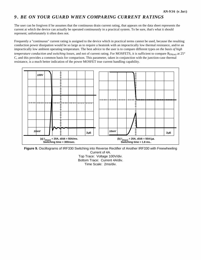
AN-936 (v.Int)
9. BE ON YOUR GUARD WHEN COMPARING CURRENT RATINGS
The user can be forgiven if he assumes that the continuous drain current rating, that appears on the data sheet represents thecurrent at which the device can actually be operated continuously in a practical system. To be sure, that's what it shouldrepresent; unfortunately it often does not.
Frequently a "continuous" current rating is assigned to the device which in practical terms cannot be used, because the resultingconduction power dissipation would be so large as to require a heatsink with an impractically low thermal resistance, and/or animpractically low ambient operating temperature. The best advice to the user is to compare different types on the basis of hightemperature conduction and switching losses, and not of current rating. For MOSFETS, it is sufficient to compare RDS(on) at 25°C, and this provides a common basis for comparison. This parameter, taken in conjunction with the junction-case thermalresistance, is a much better indication of the power MOSFET true current handling capability.
10mV 2µµS10mV 2µµS
100V
(a) I(max) = 20A, di/dt = 50A/ms.Switching time = 300nsec.
(b) I(max) = 20A, di/dt = 50A /µ/µs.Switching time = 1.8 ms..
Figure 9. Oscillograms of IRF330 Switching into Reverse Rectifier of Another IRF330 with FreewheelingCurrent of 4A.
Top Trace: Voltage 100V/div.Bottom Trace: Current 4A/div.
Time Scale: 2ms/div.

AN-949 (v.Int)
Current Ratings of Power Semiconductors
Topics Covered:
What is a current rating?Current ratings for power semiconductorsContinuous current ratingsCurrent ratings under duty cycle conditionsTransient thermal impedancePeak Current Ratings of Power SemiconductorsRMS values of common waveforms
1. WHAT IS A CURRENT RATING?
The current rating of an electrical device, be that a circuit breaker or a motor or a transformer, is the current at which thetemperature within the electrical device reaches a value that may impair the reliability or functionality of the device itself. Themanufacturer knows the temperature limits of the materials used in the device, but he does not know the temperature of theambient in which the device will be used. So he makes an assumption on this temperature. This has two important consequences:
1. A current rating is meaningless without the rated temperature2. The temperature at wich the rating applies may, or may not be related to actual operating conditions. If it is, the
current rating can be used as an indication of the current capability of that device in a real applications. If the device israted at a temperature that is not encountered in a typical operating environment, e.g. 25ºC, it cannot be trusted toprovide an indication of actual device capability in an application. It can only be used to compare the ratings ofsimilar devices rated at the same temperature.
The rating of electrical devices like motors and circuit breakers are dictated by various agreements and regulations. The ratingsof many other devices, like transformers, resistors and semiconductors are specified in their data sheets. As a result, the usermust do, at a minimum, a verification that the device is capable of operating:
a) at the maximum currentb) at the maximum ambient temperaturec) without exceeding its maximum temperature
2. CURRENT RATINGS FOR POWER SEMICONDUCTORS
Like any other electrical device, power semiconductors must be operated within their maximum temperature. Since the vastmajority of power semiconductors operate at large power densities, they need to be heatsunk. It is the task of the designer toidentify the heatsink, or other cooling method, that fulfills the requirements a, b and c of the previous section. This task isnormally referred to as “thermal design”.
Power semiconductors have, however, some additional limitations normally associated with their capability of handling highvoltages and high currents at the same time, under static or dynamic conditions. These limitations are peculiar to the specifictype of semiconductor, e.g. SOA for transistors, dv/dt, di/dt and tq for tyristors, trr for diodes. Information on these limitations arenormally contained in publications that are specific to the particular device.
Bipolar transistors have one additional limitation that is not common to other power semiconductors: gain. To operate a bipolartransistor at its headlined “rated” continuous current would require an inconveniently large amount of drive current, and thesaturation voltage and switching times would be hard to live with in a practical design.
Other power semiconductors are not limited by gain. IGBT for motor drive applications are, by design, limited in gain to currentlevels much beyond normal operating conditions to reduce the current under short-circuit conditions.
John P Taylor
http://www.irf.com/technical-info/appnotes/an-949.pdf

AN-949 (v.Int)
3. CONTINUOUS CURRENT RATINGS
The continuous rating of a power semiconductor is based is heat removal when conducting a fixed amount of current. This isdetermined by the fundamental equation for temperature rise (see INT-936), with no switching losses present. Rated ID, for aMOSFET is therefore:
where RDS(on) is the limiting value of the on-resistance at rated T(Jmax] , at the appropriate value of ID. RthJC is the maximumvalue of internal junction-to-case thermal resistance, and Tc is the case temperature.
Similarly, the continuous current rating of a diode, or a thyristor, or an IGBT is calculated from the basic equation of temperaturerise. The power dissipation is calculated from voltage drop and continuous current.
Except for water-cooled sinks, it is very difficult to keep the case temperature of a power semiconductor at less than 90º. Thus,the usable continuous direct current of a power device for most practical is whatever is applicable to a case temperature of 90 to110° C. This allows a sufficient differential between case and ambient temperature for the heat dissipator to handle the heattransfer.
The “headlined” continuous current rating shown on the data sheets of most power transistors is usually larger than the abovepractically usable level of continuous drain current. This is because the case temperature adopted by the industry, to which the“headlined” continuous ID rating applies, is 25°C.
Figure 1 shows typical heatsinks for TO-3 and TO-220 packaged HEXFET®s that allow them to operate in a 40°C ambient at acontinuous direct drain current that is 60 to 70% of the rated continuous drain current at Tc = 25°C; the corresponding steadycase temperature is about 100°C.
The continuous current rating of power transistors is, however, of little direct use to the designer, other than as a benchmark, forthe following three reasons:
1. Power transistors are normally operated in switchmode, with duty cycles considerably less than l00%, and what is reallyof interest is the current-carrying capability of the device under the actual “switched” operating conditions.
2. When operated in switchmode, power transistors have switching losses, that have to be calculated and added to the
conduction losses, as indicated in INT-936. 3. The selection of the power device may be dictated by surge requirements that make the continuous current rating
irrelevant.
And, if this were not enough, advances in the low-voltage MOSFET technology have reduced conduction losses to the point thatthe package has become the limiting factor in their continuous current rating. This is explained in INTDT93-4
4. SWITCHING “DUTY CYCLE” RATINGS
The basic thermal equation of INT-936 determines the basic rating of a “thermal system” in a practical application. Thisequation can be used to determine how much power can be dissipated by a (known) thermal system or the junction temperaturefor a given set of electrical operating conditions (power dissipation). Since the power entered in that equation is the “average”power, it remains valid as long as the frequency of operation is high with respect to the thermal inertia of the system. When thefrequency is very low (tens of Hz), the transient thermal response curve is used, as described below in Section 5.
The power dissipation is normally divided in conduction and switching. Conduction losses in a power MOSFET, being resistivein nature, can be calculated as (IRMS)2 x R. The RMS content of waveforms of different shape can be found in the Appendix.Switching losses can be calculated from the switching waveforms, from the gate charge or from analytical methods. Conductionand switching losses for IGBTs are more complex, as explained in INT-990.
I = T - T
R RDJMAX C
DS(on) th(JC)

AN-949 (v.Int)
5. JUNCTION TEMPERATURE UNDER PULSED CONDITIONS
Under surge conditions the junction temperature risesexponentially, according to its thermal inertia. Rather than usingthe thermal resistance, that is appropriate for steady stateoperation, we use the Transient Thermal Impedance (or, morecorrectly, Thermal Response Curve), as the one shown in Figure2. For a surge of given duration (x axis), this curve gives athermal response factor (y axis). The peak junction temperaturedue to the surge condition can be calculated as indicated in thefigure itself. The power dissipation is normally calculated fromthe voltage and current across the device during the surge.
This curve is also useful for determining the peak junctiontemperature for power or pulses with a very low repetition rate,when the method described in the previous section is notapplicable The reason for this is illustrated by the waveforms inFigures 3(a) and 3(b). Both sets of waveforms are for the samepower dissipation and duty cycle, but for different operatingfrequencies. The cycle-by-cycle fluctuations of junctiontemperature at 20Hz (Figure 3a) are clearly greater than at 200Hz(Figure 3b). As frequency increases, thermal inertia of thejunction “irons out” instantaneous temperature fluctuations, andthe junction responds more to average, rather than peak powerdissipation. At frequencies above a few kHz and duty cycles above20% or so, cycle-by-cycle temperature fluctuations become small,and peak junction temperature rise becomes equal to the averagepower dissipation multiplied by the DC junction-to-case thermalresistance, within one or two percent.
For pulses with low repetition rate the remaining curves in Figure2 show effective thermal impedance at different duty cycles. Thesecurves are approximately related to the single pulse curve, by thefollowing relationship:
Effective normalized thermal impedance = D + (l - D) x (transientthermal impedance for single pulse of duration t).
The thermal impedance, when multiplied by the power dissipationduring the conduction period t (i.e., the power within theconduction pulse itself, not the power averaged over the wholecycle), gives the value of the repetitive peak junction-to-casetemperature rise.
To determine the absolute value of the peak junction temperature,it is, of course, necessary to know the case temperature TC understeady-state operating conditions. Because of thermal inertia, theheatsink responds only to average power dissipation (except atextremely low frequencies which generally will not be of practicalinterest). TC is therefore given by:TC = TA + (RthC-S + RthS-A) PAV
where:TA = ambient temperatureRthC-S = case-to-sink thermal resistanceRthS-A = sink-to-ambient thermal resistancePAV = average power dissipationalso,PAV = peak power x duty cycle for rectangular pulses of power
(a) Type 621-A heatsink give 4A continuous rating forIRF331 with 5 CFM airflow in 400C ambient.
(b) Type 641-A heatsink gives 3.5A continuous ratingfor IRF331 with natural convection cooling in 400C
ambient.
(c) Type 689-75 e4 heatsink give 1A continuous ratingfor IRF710 with natural convection cooling in 400C
ambient.
Figure 1. Typical Heatsinks for HEXFETs(Heatsink by Wakefield)

AN-949 (v.Int)The transient thermal response curve assumes constant case temperature. This is generally valid for pulses shorter than 10ms.For longer surges the case temperature starts to rise and the results are of questionable accuracy. For operation in free air, casetemperature starts to rise within few ms and this curve does not provide any useful information. More sophisticated analyticalmethods that take the entire thermal system into account are normally used to calculate temperature rise under these conditions.
0-0.5
0.2
0.1
0.05
0.02
0.01SINGLE PULSE
(THERMAL RESPONSE)
NOTES:1. DUTY FACTOR, D-t1/t2
2. PEAK TJ-PDM x ZthJC + TC
t1t2
PDM
10-5 10-4 10-3 10-2 0.1 1 1010-2
0.1
1
10
t1, Rectangular Pulse Duration (seconds)
The
rmal
Res
pons
e (Z
θθJC
)
Figure 2. Transient Thermal Impedance Curves for IRF530 HEXFET
∆∆TJ = 640C
t = 10ms
100WPOWER
JUNCTIONTEMPRISE
(a) t = 10 ms D = 0.2
100WPOWER
JUNCTIONTEMPRISE
t = 1ms
∆∆TJ = 33.40CAVERAGE
(b) t = 1 ms D = 0.2
Figure 3. Waveforms of Power and Junction Temperature for Repetitive Operation,showing that Peak Junction Temperature is function of Operating Frequency. IRF330

AN-949 (v.Int)
6. PEAK CURRENT RATINGS
IGBTs and MOSFETs are able tocarry peak current well in excess oftheir continuous current rating,provided that the rated junctiontemperature is not exceeded. There is,however, an upper limit on thepermissible current, defined by therated peak current. Most devices havea peak rating, that is several timestheir continuous rating at Tc =25°C.
Power transistors are fundamentally“linear” devices, as opposed to“latching” devices. As currentincreases, the point eventually isreached at which they go into “linear”
operation and start to act, in effect, asa current limiter. This point dependsupon the drive voltage applied to thegate, the safe limit of which isdetermined by the thickness of theoxide that insulates the gate from thebody of the device. Peak ratings ofpower devices are normallyachievable with an applied gate voltage that is equal to the maximum permissible gate voltage of 20V. They are repetitiveratings, as long as the junction temperature is kept within the rated TJmax. Peak junction temperature can be calculated from thethermal impedance data for the device, as indicated above.
It should be pointed out that the on-resistance of any MOSFET does increase as current increases. As shown in Figure 4, the on-resistance of a 100V rated HEXFET® at its rated IDM with 20V applied to the gate is typically 1.4 x the value at the rated ID; thecorresponding multiplier for a 400V rated HEXFET® is 2.9. This increase of on-resistance must, of course, be taken into accountwhen making thermal calculations and designing for use of the IDM rating.
APPENDIX
Determining the RMS Value of ID WaveformsTo accurately determine the conduction losses in a MOSFET, the RMS value for ID must be known. The current waveforms are
rarely simple sinusoids or rectangles, and this can pose some problems in determing the value for IRMS. The following equations
and procedure can be used to determine IRMS for any waveform that can be broken up into segments for which the RMS valuecan be calculated individually.
The RMS value of any waveform is defined as I RMS = I 2(t)dt0
t
T
∫(1)
Figure A-1 shows several simple waveforms and the derivation for IRMS using equation (1).
If the actual waveform can be approximated satisfactorily by combining the waveforms in Figure A-1, then the RMS value of the
waveform can be calculated from: I RMS I RMS I RMS I RMS N= + + ⋅⋅ ⋅ +21
22
2( ) ( ) ( ) (2)
This is true to the extent that no two waveforms are different from zero at the same time.In some applications such as switching regulators, it is possible for the designer to control the wave shape with topology ormagnetic design. This can be very beneficial in reducing the value for IRMS in the switch for a given value of average current.
3
2
1
00 20 40 60 80 100
100VHEXFET VGS = 20V
VGS = 20V400VHEXFET
400V HEXFET
VGS = 10VVGS = 10V100VHEXFET
%IDMRated ID @ TC = 250C
PE
R U
NIT
RD
S(o
n)
Figure 4. Typical Variation of On-Resistance with Drain Current.

AN-949 (v.Int)
EFFECT OF WAVEFORM SHAPE ON RMS VALUE
In a swith mode converter, the current waveforms through the inductors, transformer windings rectifiers and switches will appearas shown in Figure A-1, ranging from a triangle to a rectangle depending on the value of the averaging inductor and load.
The RMS content of the current waveform changes accordingly and this has a bearing on the MOSFET conduction losses that areproportional to I2RMS.
A measure of the squareness of the waveform can be obtained from the ratio: KI
Ia
b=
It can be shown that: KI
If L, La
bc= = ( ) where:
L = inductance of the averaging choke.Lc = l is the critical inductance for a
particular input voltage and loadpower.
As L is increased, K goes from 0 (triangle) to 1(rectangle).
From the above expression and II I
avga b=
+2
we have: IK
KIa avg=
+2
1,
IK
Ib avg=+2
1
Substituting into the RMS expression for atrapezoidal waveform, shown in Figure A-1, wehave:
I DK K
KRMS avg=
+ ++
21
3 1
2
2 I( )
For constant I(avg) and D, the normalized (IRMS =1 for K = 1) IRMS is as shown in Figure A-3. Thiscurve shows that, for trianglar current waveforms,the I2R losses are 32% higher than for rectangular
waveforms. It is also apparent that for Ia / Ib > 0.6,the improvement incurred by increasing L is only2%, so from a practical point of view, L need onlybe about twice Lc.
Increasing the value of Ia / Ib increases the switchturn-on losses but decreases the turn-off losses.Since the turn-off losses tend to be larger than theturn-on losses, increasing Ia / Ib reduces the totalswitching loss also.For the case of discontinuous inductor currcnt (L< Lc), Ia / Ib = 0 and is no longer relevant, sincethe waveforms are now triangles.
I1
T = T FULL WAVESINUSOIDAL
T
I1
T
T
PULSEDSINUSOIDAL
PHASECONTROLLEDSINUSOIDAL
T
T
I1
t1
I1
T
IbIa
T RECTANGULAR
T
I1
T TRIANGLE
IRMS = I1D2
D =T
T
D = 1 -t1T
D =T
T
IRMS = I1D3
D =T
T
IRMS = I1D2
+ sin T (1-D) cos ΠΠ (1-D)2ΠΠ
1/2
IRMS =I1
2
IRMS = D ( Ib2 + Ia Ib + Ia
2)/31/2
D =T
T
IRMS = I1 D
Figure A-1

AN-949 (v.Int)
LARGE L
SMALL L
Ib
IbIa
Figure A-2. Current Waveform
1.16
1.14
1.12
1.10
1.08
1.06
1.04
1.02
1
00 0.1 0.2 0.3 0.4 0.5 0.6 0.7 0.8 0.9 1.0
K = Ia / Ib
I RM
S N
OR
MA
LIZ
ED
Figure A-3. Variation of IRMS with Squareness Ratio

AN-937 (v.Int)
Gate Drive Characteristics and Requirements forHEXFET®s
Topics covered:Gate drive vs base driveEnhancement vs DepletionN vs P-ChannelMax gate voltageZener diodes on gate?The most important factor in gate drive: the impedance of the gate drive circuitSwitching 101 or Understanding the waveformsWhat happens if gate drive impedance is high? dv/dt induced turn-onCan a TTL gate drive a standard HEXFET®?The universal bufferPower dissipation of the gate drive circuit is seldom a problemCan a C-MOS gate drive a standard HEXFET®?Driving HEXFET®s from linear circuitsDrive circuits not referenced to groundGate drivers with optocouplersGate drive supply developed from the drain of the power deviceGate drivers with pulse transformersGate drivers with choppersDrive requirements of Logic Level HEXFET®sHow fast is a Logic Level HEXFET®driven by a logic circuit?Simple and inexpensive isolated gate drive suppliesA well-kept secret: Photovoltaic generators as gate driversDriving in the MHz? Use resonant gate driversRelated topics
(Note: Most of the gate drive considerations and circuits are equally applicable to IGBTs. Only MOSFETs are mentioned for thesake of simplicity. Special considerations for IGBTs are contained in INT-990)
1. GATE DRIVE VS BASE DRIVE
The conventional bipolartransistor is a current-drivendevice. As illustrated inFigure 1(a). a current mustbe applied between the baseand emitter terminals to pro-duce a flow of current in thecollector. The amount of adrive required to produce agiven output depends uponthe gain, but invariably acurrent must be made to flowinto the base terminal toproduce a flow of current inthe collector.
The HEXFET®is fundamentally different: it is a voltage-controlled power MOSFET device. A voltage must be applied betweenthe gate and source terminals to produce a flow of current in the drain (see Figure 1b). The gate is isolated electrically from thesource by a layer of silicon dioxide. Theoretically, therefore, no current flows into the gate when a DC voltage is applied to it -though in practice there will be an extremely small current, in the order of nanoamperes. With no voltage applied between thegate and source electrodes, the impedance between the drain and source terminals is very high, and only the leakage currentflows in the drain.
IC
IB
CURRENTSOURCE
CURRENTIN BASE
PRODUCESCURRENTIN COLLECTOR
ID
VOLTAGESOURCE
VOLTAGEAT GATE
PRODUCESCURRENTIN DRAIN
+++
(a) Bipolar Transistor (b) HEXFET
Figure 1. Bipolar Transistor is Current Driven, HEXFET is Voltage Driven
John P Taylor
http://www.irf.com/technical-info/appnotes/an-937.pdf

AN-937 (v.Int)
When a voltage is applied between the gate andsource terminals, an electric field is set up within theHEXFET®. This field “inverts” the channel (Figure2) from P to N, so that a current can flow from drainto source in an uninterrupted sequence of N-typesilicon (drain-channel-source). Field-effecttransistors can be of two types: enhancement modeand depletion mode. Enhancement-mode devicesneed a gate voltage of the same sign as the drainvoltage in order to pass current.
Depletion-mode devices are naturally on and areturned off by a gate voltage of the same polarity asthe drain voltage. All HEXFET®s are enhancement-mode devices.
All MOSFET voltages are referenced to the sourceterminal. An N-Channel device, like an NPNtransistor, has a drain voltage that is positive withrespect to the source. Being enhancement-modedevices, they will be turned on by a positive voltageon the gate. The opposite is true for P-Channeldevices, that are similar to PNP transistors.Although it is common knowledge that HEXFET®transistors are more easily driven than bipolars, a few basic considerationshave to be kept in mind in order to avoid a loss in performance or outright device failure.
2. GATE VOLTAGE LIMITATIONS
Figure 2 shows the basic HEXFET®structure. The silicon oxide layer between the gate and the source regions can be puncturedby exceeding its dielectric strength. The data sheet rating for the gate-to-source voltage is between 10 and 30 V for mostHEXFET®s.Care should be exercised not to exceed the gate-to-source maximum voltage rating. Even if the applied gate voltage is kept belowthe maximum rated gate voltage, the stray inductance of the gate connection, coupled with the gate capacitance, may generateringing voltages that could lead to the destruction of the oxide layer. Overvoltages can also be coupled through the drain-gateself-capacitance due to transients in the drain circuit. A gate drive circuit with very low impedance insures that the gate voltageis not exceeded in normal operation. This is explained in more detail in the next section.
Zeners are frequently used “to protect the gate from transients”. Unfortunately they also contribute to oscillations and have beenknown to cause device failures. A transient can get to the gate from the drive side or from the drain side. In either case, it wouldbe an indication of a more fundamental problem: a high impedance drive circuit. A zener would compound this problem, ratherthan solving it. Sometimes a zener is added to reduce the ringing generated by the leakage of a gate drive transformer, incombination with the input capacitance of the MOSFET. If this is necessary, it is advisable to insert a small series resistor (5-10Ohms) between the zener and the gate, to prevent oscillations.
3. THE IMPEDANCE OF THE GATE CIRCUIT
To turn on a power MOSFET a certain charge has to be supplied to the gate to raise it to the desired voltage, whether in thelinear region, or in the “saturation” (fully enhanced) region. The best way to achieve this is by means of a voltage source, capableof supplying any amount of current in the shortest possible time. If the device is operated as a switch, a large transient currentcapability of the drive circuit reduces the time spent in the linear region, thereby reducing the switching losses.
On the other hand, if the device is operated in the linear mode, a large current from the gate drive circuit minimizes therelevance of the Miller effect, improving the bandwidth of the stage and reducing the harmonic distortion. This can be betterunderstood by analyzing the basic switching waveforms at turn-on and turn-off for a clamped inductive load, as shown in Figures
DRAIN DRAIN
DIODE CURRENT
TRANSISTORCURRENT
TRANSISTORCURRENT
NSOURCE
NGATE OXIDE
P
N
INSULATINGOXIDE
SOURCEMETALLIZATION
SILICON GATECHANNEL
Figure 2. Basic HEXFET Structure

AN-937 (v.Int)
3 and 5. Figure 3 shows the waveforms of the drain current, drain-to-source voltage and gate voltage during the turn-on interval.For the sake of simplicity, the equivalent impedance of the drive circuit has been assumed as purely resistive.
At time, t0, the drive pulse starts to rise. At t0 it reaches the threshold voltage of the HEXFET®s and the drain current starts toincrease. At this point, two things happen which make the gate-source voltage waveform deviate from its original “path”. First,inductance in series with the source which is common to the gate circuit (“common source inductance”) develops an inducedvoltage as a result of the increasing source current. This voltage counteracts the applied gate drive voltage, and slows down therate of rise of voltage appearing directly across the gate and source terminals; this in turn slows down the rate of rise of thesource current. This is a negative feedback effect: increasing current in the source produces a counteractive voltage at the gate,which tends to resist the change of current.
The second factor that influences the gate-source voltage is the so called “Miller” effect. During the period t1 to t2 some voltageis dropped across “unclamped” stray circuit inductance in series with the drain, and the drain-source voltage starts to fall. The
LOAD
"OPEN CIRCUIT"DRIVEPULSE
DRIVE CIRCUITRESISTANCE
G
INDUCTANCESTRAY
SOURCESOURCEINDUCTANCE
DRAIN-SOURCEVOLTAGE
DRAIN-SOURCE
VTH
"OPEN CIRCUIT" DRIVE PULSE
GATE-SOURCEVOLTAGE
I
t0 t1 t3t2 t4
Figure 3. Waveforms at Turn-On
DRIVE
+
- ID
+
-IS
THIS INDUCED VOLTAGESUBSTRACTS FROM THEDRIVE VOLTAGERESULTING IN
RESULTING INTHIS VOLTAGE RISING
MORE SLOWLYRESULTING IN
SLOW RISE OF IS
VOLTAGE DROP ACROSSTHIS L MEANS THAT THE
DRAIN VOLTAGE FALLRESULTING IN
DISCHARGE OFTHIS CAPACITOR
RESULTING INMORE CURRENT
THROUGH THISRESISTANCE
Figure 4. Diagrammatic Representation of EffectsWhen Switching-ON
DRAIN-SOURCEVOLTAGE
G-S VOLTAGE
CURRENT
GATE VOLTAGEGIVING IVTH
"OPEN CIRCUIT"DRIVE PULSE
t4t3t2t1t0
I
Figure 5. Waveforms at Turn-OFF

AN-937 (v.Int)
decreasing drain-source voltage is reflected across the drain-gate capacitance, pulling a discharge current through it, andincreasing the effective capacitive load on the drive circuit.This in turn increases the voltage drop across the source impedance of the drive circuit, and decreases the rate of rise of voltageappearing between the gate and source terminals. Obviously, the lower the impedance of the gate drive circuit, the less this effectwill be. This also is a negative feedback effect; increasing current in the drain results in a fall of drain-to-source voltage, which inturn slows down the rise of gate-source voltage, and tends to resist the increase of drain current. These effects are illustrateddiagramatically in Figure 4. This state of affairs continues throughout the period t1 to t2, as the current in the HEXFET®rises to
the level of the current, IM, already flowing in the freewheeling rectifier, and it continues into the next period, t2 to t3, when thefreewheeling rectifier goes into reverse recovery.
Finally, at time t3 the freewheeling rectifier starts to support voltage and drain current and voltage start to fall. The rate of fall ofdrain voltage is now governed almost exclusively by the Miller effect, and an equilibrium condition is reached, under which thedrain voltage falls at just the rate necessary for the voltage between gate and source terminals to satisfy the level of drain currentestab-lished by the load. This is why the gate-to-source voltage falls as the recovery current of the freewheeling rectifier falls,then stays constant at a level corresponding to the drain current, while the drain voltage falls. Obviously, the lower the impe-dance of the gate-drive circuit, the higher the discharge current through the drain-gate self-capacitance, the faster will be the falltime of the drain voltage and the switchinglosses.
Finally, at time t4, the HEXFET®is switched fullyon, and the gate-to-source voltage rises rapidlytowards the applied “open circuit” value.
Similar considerations apply to the turn-offinterval. Figure 5 shows theoretical waveformsfor the HEXFET®in the circuit of Figure 4 duringthe turn-off interval. At to the gate drive starts to
fall until, at tl , the gate voltage reaches a levelthat just sustains the drain current and the deviceenters the linear mode of operation. The drain-to-source voltage now starts to rise. The Millereffect governs the rate-of-rise of drain voltageand holds the gate-to-source voltage at a levelcorresponding to the constant drain current.Once again, the lower the impedance of the drivecircuit, the greater the charging current into thedrain-gate capacitance, and the faster will be therise time of the drain voltage. At t3 the rise ofdrain voltage is complete, and the gate voltageand drain current start to fall at a rate determinedby the gate-source circuit impedance.
We have seen how and why a low gate driveimpedance is important to achieve highswitching performance. However, even whenswitching performance is of no great concern, itis important to minimize the impedance in thegate drive circuit to clamp unwanted voltagetransients on the gate. With reference to Figure6, when one HEXFET®is turned on or off, a stepof voltage is applied between drain and source ofthe other device on the same leg. This step ofvoltage is coupled to the gate through the gate-to-drain capacitance, and it can be large enough toturn the device on for a short instant (“dv/dtinduced turn-on”). A low gate drive impedance would keep the voltage coupled to the gate below the threshold.
A STEP OF VOLTAGE CAUSES
VDS Q1
VDS Q2
VGS Q1
VGS Q2
A TRANSIENTON THE GATE
Figure 6. Transients of Voltage Induced on the Gate by RapidChanges on the Drain-to-Source Voltage

AN-937 (v.Int)
In summary: MOS-gated transistors should be driven from low impedance (voltage) sources, not only to reduce switching losses,but to avoid dv/dt induced turn-on and reduce the susceptibility to noise.
4. DRIVING STANDARD HEXFET®S FROM TTL
Table 1 shows the guaranteed sourcing and sinking currents for different TTL families at their respective voltages. From thistable, taking as an example of the 74LS series, it is apparent that, even with a sourcing current as low as 0.4 mA, the guaranteedlogic one voltage is 2.4V (2.7 for 74LS and 74S). This is lower than the possible threshold of a HEXFET®. The use of a pull-upresistor in the output, as shown in Figure 7, takes the drive voltage up to 5 V, as necessary to drive the gate of Logic LevelHEXFET®s, but is not sufficient to fully enhance standard HEXFET®s. Section 8 covers the drive characteristics of the logiclevel devices in detail.
LogicConditions 54 / 74 54H / 74H
(54L) /74L
(54LS) /74LS 74S
Logic ZeroMin. sink current
for VOL
16mA< 0.4V
20mA< (0.4V) /
20mA< (0.3V) /
0.4V
(4) / 8< (0.4V) /
0.5V
20mA
0.5V
Logic OneMax. source
current for VOH
-0.4mA>2.4V
-0.5mA>2.4V
-0.2mA>2.4V
-0.4mA> (2.5) /
2.7V
-1.0mA>2.7V
Typical GatePropagation Delay
10ns 7ns 50ns 12ns 4ns
Table 1. Driving HEXFET®s from TTL (Totem Pole Outputs)
Open collector buffers, like the 7406, 7407, etc., possibly withseveral drivers connected in parallel as shown in Figure 9, giveenough voltage to drive standard devices into “fullenhancement”, i.e. data sheet on-resistance. The impedance ofthis drive circuit, however, gives relative long switching times.Whenever better switching performance is required, interfacecircuits should be added to provide fast current sourcing andsinking to the gate capacitances. One simple interface circuit isthe complementary source-follower stage shown in Figure 9. Todrive a MOSFET with a gate charge of 60 nC in 60 ns an averagegate current of 1 A has to be supplied by the gate drive circuit, asindicated in INT-944. The on-resistance of the gate driveMOSFETs has to be low enough to support the desired switchingtimes.
With a gate charge of 60 nC and at a switching frequency is100kHz, the power lost in the gate drive circuit is approximately:
P = VGS x QG x f = 12 x 60 x 10-9 x 100 x 103 = 72mW
The driver devices must be capable of supplying 1A withoutsignificant voltage drop, but hardly any power is dissipated inthem.
5. DRIVING STANDARD HEXFET®S FROM C-MOS
While the same general considerations presented above for TTL would also apply to C-MOS, there are three substantialdifferences that should be kept in mind:
1. C-MOS has a more balanced source/sink characteristic that, on a first approximation, can be thought of as a 500 ohmresistance for operation over 8V and a 1k ohm for operation under 8V (Table 2).
Figure 7. Direct Drive from TTL Output
LOAD
VH
PULL-UPRESISTOR
TTL(TOTEM POLE)

AN-937 (v.Int)
2. C-MOS can operate from higher supply voltages than 5V so that HEXFET®saturation can be guaranteed.3. Switching times are longer than those for TTL (Table 2).
When C-MOS outputs are directly coupled to the gate ofa HEXFET®, the dominant limitation to performance isnot the switching time, but the internal impedance(assuming that C-MOS are operated from a 10V orhigher voltage supply). It will certainly not be able toturn OFF the HEXFET®as fast as the TTL, while theturn-ON waveform will be slightly better than what canbe achieved with a 7407 with a 680 ohm pull-upresistor. Of course, gates can be paralleled in anynumber to lower the impedance and this makes C-MOSa very simple and convenient means of drivingHEXFET®s. Drivers can also be used, like the 4049 and4050 which have a much higher current sinkingcapability (Table 2), but they do not yield any significantimprovement in current sourcing.
For better switching speeds, buffer circuits, like the oneshown in Figure 9, should be considered, not only toprovide better current sourcing and sinking capability,but also to improve over the switching times of the C-MOS output itself and the dv/dt noise immunity.
6. DRIVING HEXFET®S FROM LINEAR CIRCUITS
The complementary source follower configuration of Figure 9 can also be used in linear applications to improve drive capabilityfrom an opamp or other analog source.
Most operational amplifiers have a very limited slew rate, in the order of few V/microsec. This would limit the bandwidth to lessthan 25kHz. A larger bandwidth can be obtained with better operational amplifiers followed by a current booster, like the onesshown in Figures 10 or 11. For a system bandwidth of 1MHz, the opamp bandwidth must be significantly higher than 1MHz andits slew rate at least 30V/µs.
VH
680 ΩΩ
IRF320
7407
680 ΩΩ
12V
Figure 8. High Voltage TTL driver and its waveforms
Figure 9. Simple Interface to Drive HEXFETs from TTL
7407
1K
VH
LOAD+12V
INPUT
87
2
4
5 6
1
3
IRF7307 OR IRF7507

AN-937 (v.Int)
Standard BufferedOutputs 4049 / 4050 Drivers
Logic Supply Voltage
Logic Conditions 5V 10V 15V 5V 10V 15VLogic Zero:Approximate sink currentfor VOL < 1.5V
1.5mA 3.5mA 4mA 20mA 40mA 40mA
Logic One:Minimum source current for VOH
-0.5mA> 4.6V
-13mA> 9.5V
-3.4mA> 13.5V
-1.25mA> 2.5V
-1.25mA> 9.5V
-3.75mA> 13.5V
Typical switching times of logic drive signals:RISEFALL
100ns100ns
50ns50ns
40ns40ns
100ns40ns
50ns20ns
40ns15ns
Table 2. Driving HEXFET®s from C-MOS (Buffered)
When analog signals determine the switching frequency orduty cycle of a HEXFET®, as in PWM applications, avoltage comparator is normally used to command theswitching. Here, too, the limiting factors are the slew rate ofthe comparator and its current drive capability. Responsetimes under 40ns can be obtained at the price of low outputvoltage swing (TTL compatible). Once again, the use ofoutput buffers like the ones shown in Figures 9, may benecessary to improve drive capability and dv/dt immunity. Ifbetter switching speeds are desired. a fast op-amp should beused.
In many applications, when the HEXFET®is turned on,current transfers from a freewheeling diode into theHEXFET®. If the switching speed is high and the strayinductances in the diode path are small, this transfer canoccur in such a short time as to cause a reverse recoverycurrent in the diode high enough to short out the dc bus. Forthis reason, it may be necessary to slow down the turn-on ofthe HEXFET®while leaving the turn-off as fast as practical.Low impedance pulse shaping circuits can be used for thispurpose, like the ones in Figures 12 and 13.
7. DRIVE CIRCUITS NOTREFERENCED TO GROUND
To drive a HEXFET®into saturation, an appropriate voltagemust be applied between the gate and source. If the load isconnected between source and ground, and the drive voltage isapplied between gate and ground, the effective voltage betweengate and source decreases as the device turns on. An equilibriumpoint is reached in which the amount of current flowing in theload is such that the voltage between gate and source maintainsthat amount of drain current and no more. Under theseconditions the voltage drop across the MOSFET is certainlyhigher than the threshold voltage and the power dissipation canbe very high. For this reason, the gate drive circuit is normallyreferenced to the source rather than to the ground. There are
Figure 10. Dual Supply Op-Amp Drive Circuit
VH
LOAD
+12V
INPUTS
87
2
4
5 6
1
3
IRF7309 OR IRF7509
-
+
-12V0.1 µµFCER
FETINPUT
OPAMP
Figure 11. Single Supply Op-Amp Drive Circuit(Voltage Follower)
CA3103
VH
LOAD
+12V
87
2
4
5 6
1
3
IRF7307 OR IRF7507
-
+
0.1 µµFCER
FETINPUT
OP AMP.
2
3

AN-937 (v.Int)
basically three ways of developing a gate drive signal that is referenced to a floating point:
1. By means of optically coupled isolators.2. By means of pulse transformers.
By means of DC to DC chopper circuits with transformer isolation.
7.1 MGDs with optocouplers
Most optocouplers require a separatesupply grounded to the source on thereceiving end of the optical link anda booster stage at the output, asshown in Figure 14a. One of themajor difficulties encountered in theuse of optocouplers is theirsusceptibility to noise. This is ofparticular relevance in applicationswhere high currents are beingswitched rapidly. Because of thedv/dt seen by the VEE pin, theoptocoupler needs to be rated forhigh dv/dt, in the order of 10 V/ns.
Figure 15a shows an MGD withunder-voltage lockout and negativegate bias. When powered with a 19V floating source, the gate drivevoltage swings between +15V and -3.9V. D1 and R2 offset the emitter voltage by 3.9V. The switching waveforms shown in Figure 15b are similar to those in Figure14b except for the negative bias. Q3, D2 and R5 form the under voltage lockout circuit.
The LED D2 is used as low voltage, low current reference diode. Q3 turns on when the voltage at the anode of D2 exceeds thesum of the forward voltage of LED and the base-emitter voltage of Q3. This enables the operation of the optocoupler. Thetripping point of the under voltage lock-out circuit is 17.5V. The start-up wave forms are shown in Figure 16.
Figure 12. A pulse shaper. The 555 is used as an illustration of a Schmitt Trigger pulse shaper
INPUT PULSE
T = RC
WITH DIODECONNECTEDAS SHOWN
VH
LOAD
+12V
87
2
4
5 6
1
3
IRF7307 OR IRF7507
C
555
8
42
36
1 R
4.7K
INPUT
Figure 13. Pulse shaper implemented with an integrator
VH
LOAD
+12V
87
2
4
5 6
1
3
C
INPUTCA3103-
+
C
R
VINPUT
WITH DIODECONNECTEDAS SHOWN
SLOPE OF VRC V/SEC

AN-937 (v.Int)
The auxiliary supply for the optocoupler and its associated circuitry can be developed from the drain voltage of the MOSFETitself, as shown in Figure 17, 18 and 19. This supply can be used in conjunction with the UV-lockout shown in Figure 15 toprovide a simple high-quality optoisolated drive.
The circuit in Figure 17a can be modified to provide higheroutput current. By changing C1 to 680pF and R3 to 5.6k, itsperformance changes to what is shown in Figures 20, 21 and22. Other methods of developing isolated supplies are discussedin Section 9.
7.2 Pulse transformers
A pulse transformer is, in principle, a simple, reliable andhighly noise-immune method of providing isolated gate drive.Unfortunately it has many limitations that must be overcomewith additional components. A transformer can only transfer tothe secondary the AC component of the input signal.Consequently, their output voltage swings from negative topositive by an amount that changes with the duty cycle, asshown in Figure 23. As a stand-alone component they can beused for duty cycles between 35 and 65%.
Figure 14a. Simple high current optoisolated driver
87
2
4
5 6
1
3
+ C210
BATT115V
GATE
EMITTER3.9V
C10.1
IRF7307 OR IRF7507
VCC
OUT
EN
VEEC
A8
7
6
5
ISO1R1 2
3
3.3k
Input: 5V/div
Output : 5V/div
Horiz: 500ns/div
Figure 14b: Waveforms associated with thecircuit of Figure 14a when loaded with 100nF
Figure 15a: Optoisolated driver with UV lockout and negative gate bias
87
2
4
5 6
1
3C210
BATT119V
GATE
EMITTER
3.9V
C10.1
IRF7309 OR IRF7509
VCC
OUT
EN
VEEC
A8
7
6
5
ISO1R1 2
3
3.3k
R310k
Q3R5
R41K
D2LED
R54.7K
1K D13.9V
C310
HCPL2200 2N2222
UNDERVOLTAGELOCK-OUT
OUTPUTBUFFER
SINGLE TO SPLITPOWER SUPPLY
IN+
IN-

AN-937 (v.Int)
Input: 5V/div
Output : 5V/div
Horiz: 500ns/divFigure 15b: Waveforms of the circuit in Figure 21a
when loaded with 100nF
FILE: 01A-POL.DAT
VBATT1 5V/div
Output: 5V/div
Horiz: 20ms/div File: 01-UV.datFigure 16. Start-up waveforms for the
circuit of Figure 15a.
Gate Voltage: 10V/div
C2 ripple voltage: 0.5V/div
Q1 drain voltage: 200V/div
Horiz: 5 µµs/div File: GPS-1.plt
Figure 17b. Waveforms of the circuit in Figure23a.C1 = 100 pF, R3 = 5.6 k, f = 50 kHz
Figure 17a. Drive supply developed from the drain voltage
+15V
D315V
15VRTN
C20.1
R3D2
1N4148C1R2
100D1
1N4148
Q1IRF840
R1
10
Q2IRF840R4
RG2
DRVRTN
DRIVE
VCC(300V)
20 30 40 50 60 70 80 90 1000
1
2
3
Frequency (kHz)
Zen
er C
urre
nt (
mA
)
Figure 18 . Zener current (max output current)for the circuit in Figure 23a.
Figure 19 . Start-up voltage at 50 kHzfor the circuit in Figure 23a.
Horiz.: 500 µµs/div File: GPS-3.PLT
C2 voltage: 5V/div.

AN-937 (v.Int)
They have the additional advantage of providing a negative gate bias. One additional limitation of pulse transformers is the factthat the gate drive impedance is seriously degraded by the leakage inductance of the transformer. Best results are normallyobtained with a few turns of twisted AWG30 wire-wrap wire on a small ferrite core.
Lower gate drive impedance and a wider duty-cycle range can be obtained with the circuit in Figure 24a. In this circuit, Q1 andQ2 (a single Micro-8 package) are used to buffer the input and drive the primary of the transformer. The complementary MOSoutput stage insures low output impedance and performs wave shaping. The output stage is fed by a dc restorer made by C2 andD1 that references the signal to the positive rail. D1 and D2 are also used to generate the gate drive voltage.
The input and output wave form with 1nF load capacitance are shown in Figure 24b. The turn-on and turn-off delays are 50ns.The rise and fall times are determined by the 10 Ohm resistor and the capacitive load. This circuit will operate reliably between20 and 500 kHz, with on/off times from 0.5 to 15 microsecs.
Due to the lack of an under voltage lock-out feature, the power-up and power down behavior of the circuit is important.Intentionally C1 and C2 are much bigger in value then C3 so that the voltage across C3 rises to an adequate level during the firstincoming pulse. The power-up wave forms at 50kHz switching frequency and 50% duty cycle are shown in Figure 25. Duringthe first pulse, the output voltage is 10V only, and drops back below 10V at the fifth pulse.
Gate voltage: 10V/div.
Drain voltage: 200V/div.
C2 ripple voltage: 1V/div
Horiz: 2 µµs/div File: gps-4.plt
Figure 20. Waveforms of the circuit inFigure 23a. with C1=680pF, R3=1k,
f=100kHz.
10 20 30 40 50 60 70 80 100Frequency (kHz)
Zen
er C
urre
nt (
mA
)
Figure 21 . Zener current (max output current)for the circuit in Figure 23a.with C1 = 680pF, R3 = 1k
20
10
0
90
C2 voltage: 5V/div
Horiz: 100 µµs/div. File: GPS-6.plt
Figure 22. Start-up voltage at 100 kHz for thecircuit in Figure 23a. with C1=680pF, R3=R3=1k
0VGS
Figure 23. Volt-seconds acrosswinding must balance

AN-937 (v.Int)
8
2
4
5 6
1
3
+12V
IN
12VRTN
Q2IR7509
Q1IR7509
C1
1
T1C2
1
D1IN4148
D2
IN4148
1
Q3
2
3R2
10
R1
10Q4
1
3
2C40.1
IN
100K
E
G
1nLOAD
R3
IRFL014 OR IRFD014T1: CORE: 331X1853E2A A1=2600 (PHILIPS, OD=0.625", Ae=0.153CM^2)
PRIMARY: 17T, SEC.: 27T
Figure 24a. Improving the performance of a gate drive transformer
Figure 24b. Waveforms associated with the circuitof Figure 24a
Input: 5V/div.
Output: 5V/div.
HORIZ: 50µµS/div. FILE: X2-START.PLT
Figure 25. Waveforms during start-up for the circuit inFigure 24a.
87
2
4
5 6
1
3
+12V
12VRTN
INPUT
C1
0.1
C1
0.47
T1
1
C2
VCC
IN
FAULT
VSCOM
CS
87
65
U21
4
IR2127/8
HO
VB
2
3
R38.2K
D5
11DF6
R21K
C
G
R4220
C510n
E
D411DQ04
100K
T1: CORE: 331X185 3E2A, A1=2600 (OD=0.625", Ae=0.153 CM^2)PRIMARY: 17T, AWG 28 SEC: 27T, AWG 28
Figure 26a. Transformer-coupled MGD with UV lockout and short-circuit protection

AN-937 (v.Int)
The power down of the circuit is smooth and free from voltage spikes. When the pulse train is interrupted at the input, the C2capacitor keeps the input of the CMOS inverter high and R1 discharges C3. By the time the input to the CMOS inverter dropsbelow the threshold voltage of Q4, C3 is completely discharged the output remains low.
The addition of a MOS-Gate Driver IC improves the performance of the circuit in Figure 24a, at the expenses of prop delay. Thecircuit shown in Figure 26a has the following features:
- No secondary supply required- Propagation delay ~500ns (CL= 10nF)- Duty cycle range 5% to 85%- Nominal operating frequency 50kHz (20kHz to 100kHz)- Short circuit protection with Vce sensing. Threshold Vce = 7.5V- Undervoltage lock-out at Vcc = 9.5V- Over voltage lock out at Vcc = 20V
The short circuit protection is implemented with a Vce sensing circuit in combination with the current sense input (CS) ofIR2127/8. When the HO pin if U2 goes high R3 starts charging C5. Meanwhile the IGBT turns on, the collector voltage drops tothe saturation level, D5 goes into conduction and C5 discharges. When the collector voltage is high, D5 is reverse biased and thevoltage on C5 keeps raising. When C5 voltage exceeds 250mV the IR2127/8 shuts down the output. The fault to shut-downdelay is approximately 2 microsecs.
For operation with a large duty cycle, several options are available. The circuits described in AN-950 use a saturating transformerto transfer the drive charge to the gate. The circuit shown in Figure 28a, on the other hand, achieves operation over a wide rangeof duty cycles by using the MGD as a latch. It has the following features:
- Frequency range from DC to 900kHz.- Turn-on delay: 250ns.- Turn-off delay 200ns- Duty cycle range from 1% to 99% at 100kHz.- Under voltage and over voltage lockout.- Optional short circuit protection, as shown in Figure 26a
In the circuit of Figure 28a the transformer is small (8 turns), since it transmits only short pulses to the secondary side. TheMGD on the secondary side of the transformer is latched by the feedback resistor R4. Figures 28b and 28c show the performanceof this circuit at the two extremes of 900 kHz and 2.5 Hz
Horiz.: 500ns/div.
Output: 5V/div.
Input: 2V/div.
Figure 26b. Waveforms associated with thecircuit of Figure 26a.
Input: 5V/div.
Output: 5V/div.
IR2121 ERR pin: 5V/div.
Horiz: 1 µµs/div. FILE: X1-ERR.PLT
Figure 27. Shutdown due to high VCEsat

AN-937 (v.Int)
7.2 Chopping gate drives
Chopper circuits can maintain a gate drive signal for an indefinite period of time, have good noise immunity performance and,with some additional circuitry, the isolated supply can be avoided.
The basic operating principle is shown in Figure 29. To turn on the MOSFET, a burst of high frequency is transmitted to thesecondary side. The MOSFET is turned off by interrupting the high frequency. The diode and the bipolar transistor form acrowbar that rapidly discharges the gate.
In addition to providing the gate drive signal, the high frequency transformer is frequently used to power auxiliary circuitry, likeshort-circuit protection, thus avoiding a dedicated supply.
8. DRIVE REQUIREMENTS AND SWITCHING CHARACTERISTICS OFLOGIC LEVEL HEXFET®S
Many applications require a power MOSFET to be driven directly from 5 V logic circuitry. The on-resistance of standard powerMOSFETs is specified at 10 V gate drive, and are generally not suitable for direct interfacing to 5V logic unless an oversizedMOSFET is employed.
87
2
4
5 6
1
3
+12V
12VRTN
IN
C1
1
C2
1nF
T14.7K
R2VCC
IN
ERR
VSVSS
CS
87
65
U11
4
IR2121
HO
VB
2
3
R4 18K
R5 18K
+15V
G
C31
E
TRANSFORMER: CORE: 266CT125-3E2A, (OD=0.325", Ae=0.072cm,^2, A1=2135)
PRIMARY: 8T, AWG 28 SEC: 8T, AWG 28
Figure 28a. Transformer-coupled MGD for operation from DC to 900 kHz
R1560
R318K 15VRTN
IRF7509 OR IRF7309
Input: 2V/div.
Output: 25.ns/div.
Horiz.: 25.ns/div. File: XP-900K.PLT
Figure 28b. Waveforms associated with thecircuit of Figure 28a operated at 900 kHz
Input: 5V/div.
Output: 10V/div.
Reference 60Hz: 10V/div.
Horiz: 50ms/div. File: XP-2P5HZ.PLT
Figure 28c. Waveforms associated with the circuitof Figure 28a operated at 2.5 Hz

AN-937 (v.Int)
Logic level HEXFET®s are specifically designed for operation from 5V logic and have guaranteed on-resistance at 5 or 4.5 Vgate voltage. Some have guaranteed on-resistance at 2.7 V.
Some important considerations for driving logic level HEXFET®s are discussed in this section and typical switching performanceof these is illustrated when driven by some common logic drive circuits.
8.1 Comparison to Standard HEXFET®s
Some devices are available as Logic-level HEXFET®s as well as standard HEXFET®s. The logic-level version uses a thinner gateoxide and different doping concentrations. This has the following effects on the input characteristics:
• Gate Threshold voltage is lower.• Transconductance is higher.• Input capacitance is higher.• Gate-source breakdown voltage is lower.
While input characteristics are different, reverse transfer capacitance, on-resistance, drain-source breakdown voltage, avalancheenergy rating, and output capacitance are all essentially the same. Table 3 summarizes the essential comparisons betweenstandard and logic level HEXFET®s.
Characteristics and Ratings Standard HEXFET ®
(IRF Series)Comparable Logic Level HEXFET ®
(IRL Series)Gate Threshold Voltage VGS(on) 2 - 4V 1 - 2V
On-Resistance RDS(on)
Logic level HEXFET®has same value of RDS(on)
VGS = 5V as standard HEXFET®at VGS = 10V
RDS(on) of logic level HEXFET®also speed at VGS = 4VTransconductance gfs Typically 39% larger for logic level HEXFET®
Input Capacitance Crs Typically 33% larger for logic level HEXFET®
Output Capacitance Crss Essentially the sameReverse Transfer Capacitance Crss Essentially the sameGate Charge
Gate-Source Qgs Essentially the sameGate-Drain Qgd Essentially the sameTotal Qg Essentially same as
VGS = 10VEssentially same atVGS = 5V
Drain Source BreakdownVoltage
BVDSS Same
Continuous Drain Current ID Same
Single Pulse Avalanche EnergyEAS Same
Max. Gate-Source Voltage VGS + 20V +10V
Table 3: Essential Comparisons of Standard and Logic Level HEXFET®s
The gate charge for full enhancement of the logic level HEXFET®is, however, about the same as for a standardHEXFET®because the higher input capacitance is counteracted by lower threshold voltage and higher transconductance. Sincethe logic level HEXFET®needs only one half the gate voltage, the drive energy is only about one half of that needed for thestandard HEXFET®. Since the gate voltage is halved, the gate drive resistance needed to deliver the gate charge in a given timeis also halved, relative to a standard HEXFET®. In other words, for the same switching speed as a standard HEXFET®powerMOSFET, the drive circuit impedance for the logic level HEXFET®must be approximately halved.
The equivalence of switching times at one half the gate resistance for the logic level HEXFET®is illustrated by the typicalswitching times for the IRL540 and the IRF540 HEXFET®s shown in Table 4, using data sheet test conditions.

AN-937 (v.Int)
Gate Resistance Gate Voltage Drain Current Typical Values (ns)RG
(ΩΩ)VGS
(V)ID
(A)tD on tr tD on tr
9 10 28 15 72 40 504.5 5 28 15 72 44 56
Table 4: Typical Resistive Switching Times for IRL540 and IRF540
TTL families do not actually deliver 5V in their VOH condition, even into an open circuit. The 5V level can, however, be reachedby the addition of a pull-up resistor from the output pin to the 5V bus, as illustrated in Figure 30. Without the pull-up resistor,the RDS(on) value at VGS = 5V may not be attained, and the value specified at VGS = 4V should be used for worst case design.
8.2 Driving Logic Level HEXFET®s
The gate threshold voltage of MOSFETs decreases with temperature. At high temperature it can approach the VOL(max)
specification of the logic driver. Care should be exercised to insure that VTH(min) at the highest operating temperature is greaterthan VOL(max) of the various logic families in order to guarantee complete turn off.
55574 8
328 5
15 VCONTROL
INPUT
470LOAD
Figure 29.
+5V
LOGICINPUTS
RET
LOAD
Figure 30. Pull-up resistor usedto deliver 5V gate drive
+VDD
R1
Figure 31a. High common mode inductance
RL
D
LD
G
LS
S
LW
RET.SIG. RET.
DRIVE
+VDD
R1
Figure 31b. Minimum common modeinductance
RL
D
LD
G
LS
S
LWRET.SIG. RET.
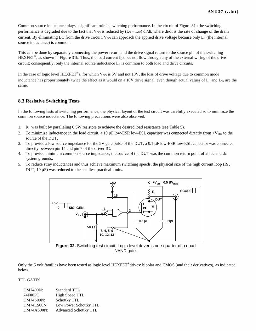
AN-937 (v.Int)
Common source inductance plays a significant role in switching performance. In the circuit of Figure 31a the switchingperformance is degraded due to the fact that VGS is reduced by (LS + LW) di/dt, where di/dt is the rate of change of the drain
current. By eliminating LW from the drive circuit, VGS can approach the applied drive voltage because only LS (the internalsource inductance) is common.
This can be done by separately connecting the power return and the drive signal return to the source pin of the switchingHEXFET®, as shown in Figure 31b. Thus, the load current ID does not flow through any of the external wiring of the drivecircuit; consequently, only the internal source inductance LS is common to both load and drive circuits.
In the case of logic level HEXFET®s, for which VGS is 5V and not 10V, the loss of drive voltage due to common mode
inductance has proportionately twice the effect as it would on a 10V drive signal, even though actual values of LS and LW are thesame.
8.3 Resistive Switching Tests
In the following tests of switching performance, the physical layout of the test circuit was carefully executed so to minimize thecommon source inductance. The following precautions were also observed:
1. RL was built by paralleling 0.5W resistors to achieve the desired load resistance (see Table 5).
2. To minimize inductance in the load circuit, a 10 µF low-ESR low-ESL capacitor was connected directly from +VDD to thesource of the DUT.
3. To provide a low source impedance for the 5V gate pulse of the DUT, a 0.1 µF low-ESR low-ESL capacitor was connecteddirectly between pin 14 and pin 7 of the driver IC.
4. To provide minimum common source impedance, the source of the DUT was the common return point of all ac and dcsystem grounds.
5. To reduce stray inductances and thus achieve maximum switching speeds, the physical size of the high current loop (RL,DUT, 10 µF) was reduced to the smallest practical limits.
Only the 5 volt families have been tested as logic level HEXFET®drives: bipolar and CMOS (and their derivatives), as indicatedbelow.
TTL GATES
DM7400N: Standard TTL74F00PC: High Speed TTLDM74S00N: Schottky TTLDM74LS00N: Low Power Schottky TTLDM74AS00N: Advanced Schottky TTL
+VDD = 0.5 BVDSS
Figure 32. Switching test circuit. Logic level driver is one-quarter of a quadNAND gate.
RL
DUT
+5V
0.1pF0.1pF
3
15
12
7, 4, 5, 910, 12, 13
50 ΩΩ
VSS
+5V0 SIG. GEN.
SCOPE

AN-937 (v.Int)
CMOS GATES
74AC00PC: Advanced CMOS74ACT00PC: TTL Compatible CMOSMM74HC00N: Micro CMOSMM74HCT00N: TTL Compatible Micro CMOS
BIPOLARDS0026: High Speed MOSFET Driver
The test conditions for the resistive switching performance is shown in Table 5. The resistive switching times obtained with theabove TTL and CMOS gates are tabulated in Table 6. In this table ton = Time in microseconds from 90% to 10% VDD and toff =
Time in microseconds from 10% to 90% VDD. Inductive switching gives faster voltage rise times than resistive switching due tothe resonant charging of the output capacitance of the device. Voltage fall times are essentially the same.
LOGIC LEVELHEXFET®
SWITCHINGVOLTAGE
(V)
SWITCHING CURRENT(A)
RDSON(ΩΩ)
RL(ΩΩ)
IRLZ14IRLZ24IRLZ34IRLZ44IRLZ514IRLZ524IRLZ524IRLZ544
3030303050505050
8162440581225
0.240.120.060.0340.600.300.180.085
3.251.51.20.79.55.94.01.9
Table 5. Resistive Switching Conditions
Logic Family Logic Level HEXFET ®,Quad, Dual Input IRLZ14 IRLZ24 IRLZ34 IRLZ44 IRL514 IRL524 IRL534 IRL544
Nand Gate ton toff ton toff ton toff ton toff ton toff ton toff ton toff ton toffDM7400NSTANDARD TTL 0.173 0.018 0.663 0.026 0.700 0.076 1.491 0.146 0.151 0.0220.238 0.041 0.263 0.060 0.616 0.124
7400FDOPCHIGH SPEED TTL 0.124 0.008 0.490 0.013 0.429 0.068 0.863 0.146 0.104 0.0040.159 0.034 0.176 0.059 0.372 0.136
DM7400SCHOTTKY TTL 0.133 0.092 0.549 0.020 0.503 0.032 1.068 0.142 0.116 0.0060.183 0.041 0.212 0.057 0.441 0.132
DM74LSLOW POWER SCHOTTKY TTL 0.174 0.038 0.778 0.093 0.706 0.146 1.438 0.342 0.155 0.0400.240 0.062 0.267 0.090 0.567 0.199
DM4SDONADVANCED SCHOTTKY TTL 0.126 0.008 0.567 0.013 0.446 0.023 0.896 0.149 0.111 0.0050.161 0.127 0.176 0.058 0.336 0.130
74ACOOPCADVANCED CMOS 0.012 0.007 0.120 0.012 0.125 0.027 0.251 0.139 0.036 0.0040.052 0.028 0.066 0.055 0.125 0.125
74ACTOOPCTTL COMPATIBLE CMOS 0.012 0.006 0.121 0.011 0.125 0.016 0.233 0.127 0.033 0.0440.052 0.027 0.060 0.055 0.120 0.122
MM74CHCOONMICRO CMOS 0.066 0.039 0.179 0.091 0.227 0.147 0.508 0.328 0.058 0.0440.092 0.068 0.111 0.096 0.232 0.213
MM74HCTCO4TTL COMPATIBLE MICRO CMOS 0.066 0.030 0.179 0.060 0.227 0.123 0.504 0.269 0.068 0.0350.092 0.051 0.111 0.086 0.232 0.186
DS0026HIGH SPEED MOSFET DRIVER 0.052 0.005 0.016 0.005 0.014 0.007 0.032 0.016 0.021 0.0040.036 0.004 0.036 0.005 0.029 0.009
Table 6. Results of the resistive load switching test
Typical Test Oscillograms
IRLZ24: 60V, 0.1 Ohm, N-Channel, TO-220 logic level HEXFET®was driven by each of the logic families listed in Table 4 andthe comparative resistive switching times photographed.

AN-937 (v.Int)
9. SIMPLE AND INEXPENSIVE METHODS TO GENERATE ISOLATEDGATE DRIVE SUPPLIES.In several applications, dc-to-dc converters are used to power the MOS Gate Driver. Although the gate drive requires littlepower, the noisy environment, the isolation voltage and creepage distance requirements and the high dv/dt between the primaryand secondary size make the design of the DC-to-DC converter somewhat complicated. Its key parameters are listed below:OUTPUT VOLTAGE, CURRENT. The output voltage of the DC-to-DC converter is the sum of the positive and negative drivevoltage to the gate. The load current required from the DC-to-DC converter is the sum of the current consumption of the drivecircuit and the average drive current to the gate.
dv/dt CAPABILITY. When the DC-DC converter powers a high sideswitch, the secondary side of theconverter is connected to the output ofthe power circuit. The rapid change ofhigh voltage at the output of powercircuit stresses the isolation of thetransformer and injects noise to theprimary side of the transformer.Switching noise at the primary sidedisturbs the operation of the converterand the control circuit for the powerstage, causing false triggering andshoot-through. Therefore atransformer with high voltageisolation, appropriate creepagedistances and low winding-to-winding capacitance is required in thisapplication.
SMALL SIZE. To reduce the interwinding capacitances the transformer must be made small. This implies operation at highfrequency. Small size and compact layout help reducing the EMI and RFI generated by the converter. Figure 33a shows aforward converter made with two CD4093 gates to generate the clock and drive the MOSFET. Energy as transferred to thesecondary when the MOSFET is on, in about 33% of the cycle. When the MOSFET is off, the secondary winding is used todemagnetize the transformer and transfer the magnetizing energy to the load, thus eliminating the need for a demagnetizingwinding. The switching waveforms are shown in Figure 33b. The ringing in the drain voltage during the fly-back period is due tothe loose coupling between the primary and the secondary windings. The load current vs. output voltage characteristic of thecircuit is shown in Figure 34. When the output current falls below 5 mA, the circuit works as flyback converter because thedemagnetizing current flows through the output. A minimum load of 5mA is required to limit the output voltage at 15V.
+12V
Figure 33a. 100 kHz Forward converter
1312
11 100
1µµF
IRFD110
1N414812K
20K
56
4
CD40931n
12VRTN
1µµF
T1
4XIN4148 V0
RL
f = 100kHz
T1 TRANSFORMER: DORE: PHILIPS 240XT250-3EA2 TOROID
(OD = 0.75", Ae=0.148CM^2, AI=3000)
PRIMARY: 14 TURNS, AWG 30 TEFLON INSULATED WIRE
SECONDARY: 24 TURNS, AWG 30 TEFLON INSULATED WIRE
Gate voltage: 5V/div.
Drain voltage: 10V/div.
Horiz: 2 µµs/div.
Figure 33b. Waveforms associated with thecircuit in Figure 33a
35
30
25
20
15
100 20 40 60 80 100 120
Load current (mA)
Out
put V
olta
ge (
V)
Figure 34. Load current vs. output voltage at 100 kHz,Rout = 27.7 Ohms

AN-937 (v.Int)
If the converter is loaded with aconstant and predictable load, a zenercan provide the necessary regulation.Otherwise a three-terminal regulatoror a small zener-driven MOSFET maybe necessary.The circuit in Figure 35a is similar tothe previous one, except that thehigher switching frequency is higher(500 kHz) and the transformer issmaller. The remaining three gates inthe package are connected in parallelto drive the MOSFET and reduce theswitching losses. The switchingwaveforms are shown in Figure 35b.The output resistance (Rout) of thiscircuit is higher than the circuit shownin Figure 33a, mainly because thestray inductance of the smaller transformer is higher and the effects of the stray inductance are higher. Figure 37a shows a push-pull operated at 500 kHz. The single gate oscillator produces a 50% duty cycle output, while the remaining gates in the packageare used to drive the push-pull output stage. The primary of the transformer sees half the voltage compared to the previouscircuit, therefore the number of turns at the primary were reduced to half.
10. PHOTOVOLTAIC GENERATORS AS GATE DRIVERS
A photovoltaic generator is a solid state power supply powered by light, normally an LED. The combination of the LED and thephotovoltaic generator in one package is called a Photovoltaic Isolator or PVI and is available in a 8-pin DIP package. As avoltage source, the PVI can function as a “dc transformer” by providing an isolated low current to a load. While an optoisolatorrequires a bias supply to transmit a signal across a galvanic barrier, the PVI actually transmits the energy across the barrier.More information on the PVI can be found in Application Note GBAN-PVI-1 which appears in the Microelectronic RelayDesigner’ s Manual. This data book also contains the data sheet for the photovoltaic isolator, the PVI1050. A circuit is alsoprovided in the AN to significantly speed up turn off of the switch. As a gate driver the PVI has significant limitations: its shortcircuit current is in the order of 30 microA with a very high internal impedance. Its simplicity, however, makes it appealing insolid-state relay replacements, where switching times are not important and switching transients are not present.
A typical application is the ac switch described below. The IGBT and the power MOSFET are not suited to switching ACwaveforms directly. The IGBT can only conduct current in one direction while the power MOSFET has an anti-parallel diodethat will conduct during every negative half-cycle. Bidirectional blocking capability can be achieved by connecting two powerMOSFETs source to source, or two IGBTs with anti-parallel diodes emitter to emitter, as shown in Figure 39.
+12V
Figure 35a. 500 kHz Forward converter
13
1211
100
1µµF
IRFD110
1N41481K
6K
56
4
CD4093220p
12VRTN
1µµF
T1
4XIN4148 V0
RL
f = 500kHz
T1: CORE: PHILIPS 266CT125-3E2A (od=0.375", Ae=0.072CM^2, AL=2135
PRIMARY: 4T, AWG 30, SECONDARY: 7T, AWG30
9
810
1
23
14
7
30
25
20
15
10
0 10 20 30 5040Load current (mA)
Out
put v
olta
ge (
V)
Figure 36. Load current vs. output voltage,Rout = 27.7 Ohms
Drain Voltage: 10V/div.
Gate voltage: 5V/div.
Horiz.: 250ns/div.
Figure 35b. Waveforms associated with thecircuit in Figure 35a

AN-937 (v.Int)
In the case of the MOSFET, there is the possibility that, for low current levels, the current flows through both MOSFETchannels, instead that one MOSFETs and diode, thereby achieving lower overall voltage drop. The MOSFET channel is abidirectional switch, that is, it can conduct current in the reverse direction.
If the voltage across the MOSFETchannel is less than the VF of theintrinsic diode (which typically has ahigher VF than discrete diodes), thenthe majority of the current will flowthrough the MOSFET channelinstead of the intrinsic diode. Thegate drive for both the MOSFETs andIGBTs must be referenced to thecommon sources or emitters of thedevices. Since this node will beswinging with the AC waveform, anisolated drive is necessary. The PVIcan be used, as shown in Figure 40.
11. RESONANT GATE DRIVE TECHNIQUES
As indicated in Section 14, gate drive losses in hard switching areequal to Qgs x Vgs x f. An IRF630 operated at 10 Mhz with agate voltage of 12 V would have gate drive losses of 3.6 W,independent from the value of the gate drive resistor. Clearly, toachieve hard switching at this frequency, the resistance of the gatedrive circuit is limited to whatever is associated with the internalimpedance of the driver and with the gate structure of the deviceitself. Furthermore, the stray inductance of the gate drive circuitmust be limited to tens of nH. The design and layout of such acircuit is not an easy task.
An alternative method to drive the gate in such an application isto design a resonant circuit that makes use of the gate capacitanceand stray inductance as its reactive components, adding whateverinductance is necessary to achieve resonance at the desiredfrequency. This method can reduce the peak of the gate drivecurrent and losses in half, while simplifying the design of the gatedrive circuit itself. Since the gate charge is not dissipated at everyswitching transition, but stored in a reactive component, the gatedrive losses are proportional to the resistance of the gate drivecircuit, rather than being independent from it. More informationon this gate drive method can be found in an article by El-Hamamsy: Design of High-Efficiency RF Class-D PowerAmplifier and in references at the end of this article (IEEETransactions on Power Electronics, May 1994, page 297).
Related Topics
MOS-Gate Driver IcsTransformer drive with wide duty cycle capabilityGate ChargeThree-phase MOS-Gate DriverPhotovoltaic Isolators (PVI)
+12V
Figure 37a. 500 kHz Forward converter
13
1211
100
1µµF10K
56
4
CD4093220p
12VRTN
1µµFT1
1N4148 V0
RL
f = 500kHz
T1: CORE: PHILIPS 266CT125-3E2A (od=0.375", Ae=0.072CM^2, AL=2135
PRIMARY: 4T, AWG 30, SECONDARY: 7T, AWG30
9
810
1
23
14
7
7, 8
2
4
5, 6
13
7T
1N4148
100nF100nF
2TIRF7307
Buffer input: 5V/div.
Buffer Output: 5V/div.
Horiz.: 500ns/div
Figure 37b. Waveforms associated with the circuit in Figure 37a
20
19
18
17
16
15
14
130 10 20 30 40 50 60
Figure 38. Load current vs. output voltage,Rout=27.7 Ohms

1
Application Note AN-1012
Mounting Considerations For International Rectifier’s Power Semiconductor Packages
by Pamela Dugdale and Arthur Woodworth, International Rectifier
Introduction It is important that power semiconductors are correctly mounted if full functionality is to be achieved. Incorrect mounting may lead to both thermal and mechanical problems. The aim of this Application Note is to describe good practise in the mounting of power semiconductors. Making Good Thermal Contact One of the major considerations when mounting all power semiconductor packages is the dissipation of heat. This is because the junction temperature of the die and the glass transition temperature of the plastic limit the performance of the device. Indeed there are maximum allowable temperatures above which the device functionality cannot be guaranteed. The way in which a device is mounted can have a large effect on the thermal contact between the header and the heat sink and hence on the ability of the package to dissipate heat. This is often referred to as the contact thermal resistance and is quoted in datasheets. A full discussion of all of the components that make up the thermal resistance of a power semiconductor package is given in International Rectifier Application Note AN-997 “Mounting Guidelines for the Super-247”. In the present note we shall concentrate on the thermal resistance between the case and the heat sink as this is the most dependent on the mounting technique.
Package Case
Heatsink
Air Gap
Figure 1. Cross section showing the source of the thermal contact resistance between a package case and the heat sink.
The physical source of the contact resistance is a result of the fact that surfaces are never perfectly flat. The recommended flatness for the mounting surface is 0.02mm in 10mm. Particular attention should be paid to ensuring that no damage occurs during the manufacture of mo unting holes. Even for two well-prepared surfaces contact only actually occurs at several points separated by large air gaps. This is shown in Figure 1. As air is a very good thermal insulator this is undesirable and increases the thermal resistance. There are two ways of reducing the volume of air trapped between the surfaces. One is to increase the force holding the two surfaces together and the other is to improve the quality of the contact area by filling in the gaps. In the case of the former this can be done by either applying a force above the die with a clip or by increasing the torque on the screw, which mounts the tab to the heatsink. The way in which the thermal resistance varies as a function of the torque on the mounting screw or the clip force is shown in Figs. 2 and 3. Over tightening the mounting screw may lead to deformation of the semiconductor package and hence an increase in the thermal resistance. This is shown in Fig. 2 which gives the thermal resistance as a function of torque for the PowIRtab™, showing a minimum at 1.1Nm for dry mounting and 0.8Nm for wet mounting. Other package types behave in a similar way. Details of how to correctly mount down a semiconductor to avoid this and other problems are given in this application note.

2
Application Note AN-1012
0
0.5
1
1.5
0 0.5 1 1.5
Torque / Nm
The
rmal
Res
ista
nce
C/W
Dry Mounting
With Heatsink Compound
Figure 2. Contact thermal resistance as a function of mounting screw torque for a PowIRtab™ package mounted to a heat sink showing both dry mounting and mounting using heat sink compound.
0
0.5
1
1.5
0 100 200 300 400
Force / N
The
rmal
Res
ista
nce
C/W
Dry Mounting
With Heatsink Compound
Figure 3. Contact thermal resistance as a function of clip force for a PowIRtab™ package mounted to a heat sink showing both dry mounting and mounting using heat sink compound. The second technique requires the use of a heat sinking compound. This is usually a silicone grease loaded with electrically insulating, thermally conductive material such as alumina. The purpose of the grease is to fill the gaps without increasing the distance between the two surfaces. If the layer of grease is too thick then the thermal resistance will be increased. To determine the correct amount of grease for a particular application a series of experiments should be performed. Several power packages and heat sinks should be assembled using different amounts of grease applied evenly to one side of each mounting surface. This can be achieved using a small rubber roller. When the amount is correct a very small amount of grease should appear around the perimeter of the device
as it is slowly torqued or clip mounted to the heat sink. Excess compound should be carefully removed. An alternative to grease is the use of thermally conductive pads. These are conformal under pressure and tend to fill the air voids in the same way as grease. The main advantage of this approach is the ease of handling, however as many of these pads are silicone based the thermal resistance of this solution tends to be higher than it would be if grease were used. In addition to this, the silicone pads provide electrical is olation, which can be either an advantage or disadvantage depending on the specific application. An alternative approach is to use a phase change material. These materials are solid until they are heated to temperatures in the range 50oC to 60oC at which point they start to flow, filling the air gaps. Such materials are available on their own or as coatings on silicone or other thermally conductive pads. For the case when electrical isolation is not required, the phase change material is available as a thin coating on aluminium foil. The relative performance of thermal grease, phase change materials and silicone conductive pads and is given in Table 1. These results were measured by International Rectifier engineers at the Assembly R&D lab.
Interface Material
Electrical Properties
Thermal Resistance Junction to Heat
Sink Heat sink Compound
Non - Conducting
0.7oC/W
Phase Change Thermal Compound
Non - Conducting
1.2oC/W
Aluminium Foil Coated in Phase Change Compound
Conducting 1.2oC/W
Thermal Interface Pad
Isolating 1.6oC/W
Thermal Interface Pad
Conducting 1.6oC/W
Table 1. Performance of thermal interface materials. Correct Mounting Procedures In this section the correct mounting procedures for the TO220 package will be discussed. This will include advice on clip mounting, screw mounting and the requirements for isolation. By

3
Application Note AN-1012
using the TO-220 as an example most of the common issues relating to the mounting of power packages will be covered. Problems that are specific to the other power packages, including the International Rectifier PowIRtab™ and Super packages, will be discussed in the next section. General Rules
• The TO-220 package should always be fastened to the heat sink before soldering the leads to the PCB.
• When bending the leads they must be clamped tightly between the package and the bending point to avoid strain on the package. The leads must be bent at a minimum distance of 2mm from the plastic for standard packages, and 3mm from the plastic for the TO-273. The TO-274 is not normally lead formed because on the design of the leg.
• The leads should be bent no more than 90o and should never be bent more than once.
• The radius of curvature should not be less than the thickness of the leads and ideally should be greater than 2 times the thickness of the leads.
• Lateral lead forming is not advisable. The pin spacing of the leads should be adhered to when mounting to a PCB.
• It is recommended that in the case where a device is rigidly secured to a PCB and also to a heat sink mounted on the PCB, a bend is put in the leads to allow for differences in thermal expansion.
• Care should be taken not to cause any mechanical damage to the package or any surface finishes.
• Heat sink compound or some other thermal interface material should be used.
Screw Mounting
• For the TO-220 a M3 screw should be used. Self-tapping screws should not be used.
• It is recommended that a rectangular washer is inserted between the screw head and the mounting tab. Care must be taken to ensure that the washer does
not damage the plastic body of the package during the mounting process.
• The recommended mounting torque is 1.1Nm. This should not be exceeded.
• When electrical isolation is required insulating pads and insulating bushes should be used.
Figures 4 and 5 show the suggested mounting hardware for the TO-220.
M3 SCREW
RECTANGULAR WASHER
DEVICE
MICA INSULATOR
HEATSINK
INSULATING BUSHPLAIN WASHERSPRING WASHER
M3 NUT
Figure 4. Screw mounting through a heat sink using a nut.
MICA INSULATOR
DEVICE
RECTANGULAR WASHER
INSULATING BUSH
M3 SCREW
HEATSINK
Figure 5. Screw mounting into a tapped heat sink.

4
Application Note AN-1012
Clip Mounting This section is applicable to the TO-220 and Super220™ (TO-273) packages.
• Using clip mounting ensures that the force is applied above the silicon and that the thermal contact is good.
Figure 6. The effect of the position of the applied force.
• Increasing the force supplied by the clip will ensure reduced thermal resistance. This is shown in Figure 3. However the increased cost of stronger clips is not always worth the performance improvements and a minimum force of 20N and typically up to 50N is recommended.
• Isolation is safely achieved by the use of an insulating pad and without the use of bushes.
• Isolation between the bond wires and the mounting clip is provided by the mould compound. The minimum thickness of plastic between a bond wire and the clip is greater than the thickness of the plastic on the header of a fullpak device. This provides 4kV dc isolation which is equivalent to 2.5kV rms ac.
• For heat sinks less than 5mm in thickness saddle clips should be used. These produce contact forces of between 15N and 50N.
Figure 7. Saddle clip mounting of a Super220™ package.
• For heat sinks greater than 5mm in thickness, U clips are used. These produce contact forces of between 15N and 50N.
Figure 8. U-Clip mounting of a Super-220™ package.
• There are a number of proprietary clip solutions where the clip is anchored in a feature in an extruded heat sink. Forces of between 25N and 50N can be achieved.
Figure 9. Customized Clip Mounting of a Super-220
Application of force off-centre (i.e. bolting a device to heatsink) leads to uneven themal contact. Using clip mounting ensures that the force is
applied above the silicon and that the thermal contact is good.
Interface material

5
Application Note AN-1012
Pop Riveting
• It is recommended that press rivets made of a soft material are used rather than pop rivets.
• The hole in the heat sink should be smaller than the device mounting hole, within acceptable tolerances. This ensures that the rivet squeezes more tightly on the heat sink than on the device,
Soldering A separate application note covers soldering down power semiconductor packages “Surface Mounting of Larger Devices.” In general devices that are being mounted to aluminium heat sinks must be either screw or clip mounted. A new technology, PowersitesTM, allows solderable power semiconductor packages to be mounted to aluminium heat sinks. Additional Information for Other Package Types
• Full-Pak devices do not require isolation pads or bushes as the package is isolated by design
• The Super220™ (TO-273) does not have a hole for screw mounting and should be mounted using clips. The ‘hole – free’ design allows the package to carry more current. Full instructions for mounting the Super220™ (TO-273) package are given in AN-1000 “Mounting Guidelines for the Super-220”
• The Super247™ (TO-274) does not have a hole for screw mounting and should be mounted using clips. The ‘hole – free’ design allows the package to carry more current. Full instructions for mounting the Super247™ (TO-274) package are given in AN-997 “Mounting Guidelines for the Super-247”
• Mounting instructions for the PowIRtab package are given in AN-1010 “PowIRtab™ Mounting Guidelines.”
• This is a high current package suitable for mounting to bus bars.
Mounting SOT227 The SOT227 is a power module with some special mounting requirements.
• The package has two mounting holes and four connection terminals.
• Fasten the device to the heat sink before connecting the leads.
• The maximum allowable torque is 1.3Nm on the terminals and on the mounting base.
• M4 screws should be used with lock washers. These are included with the packages.
• The separation of the centre of the mounting holes is 30mm ± 0.2mm. Full details of the dimensions are given on the datasheet.
• The first mounting screw should be tightened to one third of the maximum torque, the second screw should then be tightened to the same torque. Full tightening of both of the screws can then be completed.
• The case to sink thermal resistance at the recommended mounting torque is 0.05C/W for a greased surface.

6
Application Note AN-1012
Links to Suppliers of Thermal Management and Mounting Accessories Company Name
Link Suppliers of……
Aavid Thermal Technologies
www.aavid.com Interface materials, clips, heatsinks.
Austerlitz Electronic GmbH
www.austerlitz-electronic.com
Interface materials, clips, heatsinks.
Bergquist www.bergquistcompany.com
Interface materials
Chomerics www.chomerics.com Interface materials, PowerSitesTM, heatspreaders.
Fischerelektronik www.fischerelektronik.de
Heatsinks and clips.
Fujipoly www.fujipoly.com
Interface materials
Kunze-Folien www.kunze-folien.de Interface materials, clips and customized heat sinks.
R-Theta www.r-theta.com
Heat sinks
Redpoint Thermalloy www.thermalloy.com Interface materials, clips and heatsinks.
Thermagon Inc www.thermagon.com
Interface materials
Warth International www.warth.co.uk Interface materials and clips.

AN-997 (v.Int)
1
Mounting Guidelines for the SUPER-247by Andrew Sawle and Arthur Woodworth
Introduction
Born from the need to accommodate ever increasing amounts of silicon in smaller, space saving packages,the SUPER-247 now allows the same die sizes that can be put in a much larger TO-264. The SUPER-247has the same outer dimensions as the industry standard TO-247 but can dissipate more power than the TO-247 whilst occupying less space than the TO-264. This package also allows the use of efficient and reliableclip mounting methods to heatsinks. This allows designers to reduce both the size and the cost of theirsystems.
This Application Note will examine the subjects involved with clip mounting the SUPER-247 to heatsinks.
Topics Covered:A breakdown of system thermal resistance.The minimum force for a good thermal contact and the maximum force allowable before deviceparameter degradation.Wet and dry contact conditions and the effect on thermal resistance.The effect on thermal resistance of using an electrical isolator between the device and theheatsink.Typical clip types, how they work and the forces that they impart. Conclusion.
1. A Breakdown of System Thermal Resistance
The thermal resistance (Rth(junction-ambient)) of a system (system = package through to heatsink) is made upfrom a number of component parts as shown in Figure 1.1 below.
Rth(junction-case) Rth(case-sink)
Rth(sink)
Rth(sink-ambient)
Silicon DiePackage
Heatsink Block
Rth
(junc
tion-
ambi
ent)
Figure 1.1 - Build-up of Thermal Resistance in a System
The designer of a system has varying amounts of influence over the component parts of the overall thermalresistance of his design:
Ø Rth(junction-case) - this has been determined during the design and manufacture of the product.The system designer has no direct influence.
Ø Rth(case-sink) (or Contact Thermal Resistance) - determined by the size and quality of thecontact areas between the package and the sink, the use of intermediate materials and thecontact pressure. Hence, the system designer can have a large influence over this parameter.
Ø Rth(sink) and Rth(sink-ambient) - determined by heatsink design, i.e. material and shape. Systemdesigner will choose optimum sink matching both performance and cost requirements.

AN-997 (v.Int)
2
Thermal resistances for packages and heatsinks can be determined from datasheets and although the contactthermal resistances can also be taken from manufacturer’s data, this figure is generally ‘TYPICAL’ and fora single set of specified conditions. Hence, it is possible for a designer to gain better or worse contactthermal resistances depending on parameters that he prescribes. The following sections include someinformation to help the designer in improving rather than worsening contact thermal resistances in theirsystems.
2. Minimum and Maximum Contact Forces
As previously mentioned, there are a number of factors that affect the contact thermal resistance, one of thefactors being the contact force with which the package is pushed against the heatsink.
Why and How Does Contact Force Affect Thermal Resistance?
Package cases and heatsink surfaces can never be perfectly flat. Hence contact between the two will onlyoccur at several points allowing an air gap between the surfaces (as illustrated in Figure 1.2). Since air is avery good thermal insulator this means that the contact thermal resistance is much greater than it would be ifthe two surfaces were in perfect contact (no air gap). However, as the contact force (pushing the twosurfaces together) increases then so will the number of points at which the two surfaces contact one anotherand the air-gap will be reduced, in turn reducing the contact thermal resistance.
Package Case
Heatsink
Air Gap
Figure 1.2 - Diagram Showing the Effect (Under High Magnification) When Two Non-Perfect Surfaces Meet.
What is the Minimum Force that Should be Applied to Gain Good Thermal Contact?
As the contact force is increased, the contact thermal resistance decreases. However, this does NOT followa linear relationship and shows diminishing returns in thermal resistance reduction for increases in thecontact force (as shown in Figure 1.3). A rapid initial fall-off in contact thermal resistance is replaced by amore gradual reduction with increased contact force. The minimum contact force should therefore be nolower than the point at which these rapid reductions in thermal resistance end - this occurs at approximately20N.
Maximum Contact Force
The minimum contact force of 20N mentioned above is purely that, the MINIMUM force. Any forceapplied above that figure will still show gains in reduced contact thermal resistance until the maximumforce that the package can withstand before the device characteristics are altered or the package isdestroyed. This maximum limit figure has been measured to be 200N TYP. However, these gains are notfree, for in general terms a greater contact force means a larger, more expensive clamping system. A contactforce should therefore be chosen that optimises both the thermal and the cost requirements of the system.

AN-997 (v.Int)
3
0
0.2
0.4
0.6
0.8
1
1.2
1.4
1.6
1.8
2
0 20 40 60 80 100 120 140 160 180
Contact Force [N]
Co
nta
ct T
her
mal
Res
ista
nce
[°
C/W
]20N = Minimum contact force.
'Dry' Contact Condition
Figure 1.3 - Minimum Contact Force
3. Contact Conditions
As mentioned previously, the contact conditions between the package and the heatsink will affect thecontact thermal resistance. Contact conditions encompass a number of areas including: surface roughness,surface cleanliness, paint finishes and intermediate materials. The surface roughness of the heatsinkingmaterial should be no greater than 0.02mm over the area where the device is to be mounted. Surfacecleanliness during assembly of package and heatsink is imperative, even if a thermal grease or othermaterial is subsequently added. Unclean surfaces can be held apart by dirt or grease thus increasing thethermal resistance. However, normal paint finishes (up to 50 µm thick) have been shown to have little effecton thermal resistance, this therefore leaves intermediate materials as an area for discussion.
Intermediate Materials
Contact between two non-perfect surfaces will result in an air gap between them. The most common methodof overcoming this is to use a thermally conductive heatsinking compound to fill the gaps between thesurfaces and hence lower the contact thermal resistance. This compound also has the advantage that itprevents moisture from penetrating between the surfaces.
A number of different companies offer heatsinking compound, these usually consist of silicon grease loadedwith some electrically insulating, good thermally conducting material such as alumina. Thinly applied, thesecompounds are advantageous as they fill the air gaps and do not further increase the distances between thesurfaces. Thickly applied they can hold the two surfaces apart and increase the contact thermal resistance.The following graph displayed in Figure 1.4 shows the contact thermal resistance for ‘dry’ conditions (nocompound) and the thermal resistance using compound, both are plotted against contact force.
The metal heatspreader on the back of the SUPER-247 package is non-electrically isolated from the pinoutsof the device within, i.e. in the case of a MOSFET the heatspreader is the drain contact, for an IGBT thecollector. Hence in cases where devices are not electrically paralleled but share the same heatsink, it isnecessary to insert an electrically isolating material between the package and the heatsink block. Theisolator usually takes the form of a pad and many companies offer a range of pad material types and sizesdependant on requirements.

AN-997 (v.Int)
4
At the minimum stated contact force of 20 N the following contact resistances can be achieved:
Contact Conditions Rth(c-s) @ 20N Contact Force‘Dry’ (no compound) 1.2°C/WThermal Compound 0.2°C/W
The pad obviously has a direct and detrimental effect on the contact resistance as insertion adds an extraresistance into the build-up. Again, the contact thermal resistance is dependant on contact pressure. Thefollowing graph, shown in Figure 1.5, illustrates the higher thermal resistance when using an isolator pad,adding a new line to the thermal resistance curve. The isolator used to plot the line was a typical siliconeloaded pad. Therefore, it should be noted that when electrically isolating a device from a heatsink thethermal resistance of the system will increase.

AN-997 (v.Int)
5
0
0.5
1
1.5
2
2.5
3
3.5
0 50 100 150 200
Contact Force [N]
Co
nta
ct T
her
mal
Res
isit
ance
[°
C/W
] Isolator Pad
'Dry' Condition
Thermal Compound
Figure 1.5 - Contact Thermal Resistance Plotted Against Contact Force
4. Typical Clips and What They Do
Why Clips?
The use of clips for providing the contact pressure is quickly becoming popular. Clip mounting provides anumber of advantages over the more traditional screw mounting techniques:
Ø Clips provide a more uniform pressure over the entirety of the mating surfaces. Althoughscrew mounting can provide a higher pressure, the force is centred at one end of the packageand there is often a loss of coplanarity between package and heatsink.
Ø Clips are faster to apply than aligning and tightening screws.Ø Clips regulate the force applied and ensure that the same force is applied to each
package/heatsink pair. Hence there is no danger of over-tightening (deforming the packageand/or heatsink) or under-tightening (increasing the contact thermal resistance).
Clip Types
There are a number of different clip types available on the market that can be used dependant on theapplication. Following are some examples of clips and the way in which they are typically used. The ideasshown by no mean encompass all the solutions available and do not prescribe the only ways in which theclips can be used.
Saddle Clips
An example of a SUPER-247 mounted to a heatsink using a saddle clip is shown in Figure 1.6.

AN-997 (v.Int)
6
Figure 1.6 - SUPER-247 Mounted to Heatsink Using Saddle Clip
When using saddle clip type solutions, the heatsink materials are thin in cross-section, typically less than5mm in thickness. The clips push into holes cut into heatsink material and lock against the back face of theheatsink. These clips produce contact forces in the range 20-60N.
‘U’ Clips
An example of a ‘U’ Clip assembly is shown in Figure 1.7.
This clip type clamps the device and the heatsink materialtogether. Variations on this clip type allow devices to beclamped to the front and back of the heatsink block using thesame clip. ‘U’ clips typically impart forces in the 20N-40Nrange. This force is partly dependent of the thickness of theheatsink material, i.e. thicker the material, the greater theforce.
Figure 1.7 - ‘U’ Clip Assembly
Extrusion Mounted Clips
There are a number of proprietary clip solutionsoffered where the clip is anchored in a feature inthe extruded heatsink. Figure 1.8 shows onesolution type where the clip fits into a shaped slotin the heatsink material.
Figure 1.8 - Extrusion Mounted Clip (SlotAnchorage)

AN-997 (v.Int)
7
This solution can produce contact forces in therange 15 - 25N. However the shaped slot is anexpensive addition to the heatsink and thissolution type is being replaced in favour of clipsmounted between shortened heatsink fins or cliprails (as shown in Figure 1.9 below). The extrudedheatsinks are less costly and the forces that can beapplied are higher, typically in the range 25 - 50N
Figure 1.9 - Extrusion Mounted Clip (RailAnchorage)
Other Solutions
Heatsink manufacturers offer a wide range of heatsink types, usually extrusions or formed metal and at acost are willing to produce customised solutions. Some manufacturers will supply the heatsink withintegrated clip both in extruded and formed metal varieties or a combination of the two. It is also possible tohave heatsink solutions supplied with thermal compound or isolator materials already applied in the correctplaces to aid assembly.
Sources for Clip Solutions
The following are companies who can supply the types of clips/solutions discussed in this Application Note:
Redpoint Thermalloy,Cheney Manor,Swindown,Wiltshire.SN2 2QN
Avvid Thermal Technologies,Corporate Headquarters,One Kool Path,Laconia,New HampshireUSA
Austerlitz Electronic gmbh,Ludwig Feuerbach -Straβe 38,90961 Nüenburg, Postfach 1048,GERMANY

AN-997 (v.Int)
8
Relevance to TO-247 Heatsink Mounting
The clipping/mounting concepts covered in this application note for the SUPER-247 can also be applied tothe standard TO-247 package. However, it should be noted that due to the screw mounting capability of thestandard TO-247 the package to heatsink contact area is reduced and hence the contact thermal resistance isINCREASED from 0.2°C/W(SUPER-247) to 0.24°C/W(TO-247). Therefore, whilst the minimumclamping force of 20N still applies, the contact thermal resistance graph for the SUPER-247 will not.
Conclusion
The SUPER-247 package can now dissipate more power and encapsulate more silicon than the industrystandard TO-247, a package with the same footprint. It also allows for faster and less costly clip mountingto heatsinks. However, the way in which the device is mounted to the heatsink will affect the thermalperformance of the system (silicon, package and heatsink). The designer can have a direct affect on thecontact thermal resistance and the design parameters that he sets can have either a positive or adverse effecton system performance. This Application Note has discussed the need for an adequate force (20N) for goodthermal contact and the fact that intermediate materials also affect the thermal resistance. Thinly appliedthermal compound will improve the contact thermal resistance whilst electrical isolators are likely to causedeterioration in this parameter.
There are many clip/heatsink solutions available and some have been indicated in this Application Note.The chosen solution will depend on the application in which it is used and should be chosen to optimiseboth cost and thermal performance characteristics.

- 1 -
Application Note AN-1033
CALCULATING TEMPERATURE GRADIENTS IN POWER MOSFETS WITH THE “HEXRISE” PROGRAM
by Doug Butchers, International Rectifier GB Ltd.
(HEXRISE may be downloaded from: www.irgb.co.uk) www.irgb.co.uk)
INTRODUCTION This note is intended to assist with the application of the Program “HEXRISE” in practical real life cases. To use this Program effectively it is important to appreciate its scope and to be able to apply it to thermal calculations for heat sinking arrangements that extend beyond just the immediate boundaries of the power semiconductor itself. Semiconductor cooling A typical cooling arrangement for a power semiconductor device will involve the transfer of heat from its source (the junction) through many different materials and interfaces to the final cooling medium - usually air. Along the way, the generation of the temperature gradient of the junction above the ambient temperature, is a function of both the power flow and the thermal response to the different materials encountered in its course. Figure 1 shows a typical mechanical arrangement for a plastic package on a heat sink. In many cases it would be usual to have an additional isolation layer between the base of the power semiconductor and the heat sink –especially for connections requiring multiple devices.
Figure 1: Typical heatsink arrangement
Figure 1: Typical heat sink arrangement Equivalent thermal circuit Figure 2 shows an equivalent thermal circuit for the previous mechanical example with the power semiconductor having two significant thermal components-the die and the package header. There are two parameters associated with each different material section in the thermal path:
1. A thermal resistive element, Rth in K/W 2. A thermal capacity element, Cth in Ws/g.K
Rth J-B
Rth Htsk-amb.
Header
TJ
"Plastic"
T amb
Die
Die attach
T ht-sk
T base

- 2 -
Application Note AN-1033
Figure 2: Equivalent thermal circuit
Figure 2: Equivalent thermal circuit The thermal resistance element is responsible for the steady-state temperature difference across the section in question while the thermal capacity element is responsible for storing heat energy at a given rate, thereby introducing a time function which delays the establishing thermal gradient. The combination of these two elements has a direct analogy to an electrical circuit containing resistance and capacitance. The Rth x Cth product is the thermal time constant with similar properties to the electrical time constant. Alternative thermal approach With HEXRISE, the thermal response characteristics of the semiconductor is modelled in a more easily accessible way than above. The device thermal parameters (steady–state and transient) are derived from the data sheet transient resistance characteristic - readily available from every device data sheet. (more in the following section.) Also, unlike the equivalent thermal circuit, the use of the data sheet thermal resistance characteristics makes a knowledge of the separate die and header thermal performance parameters unnecessary since the curve reflects the true transient and steady-state performance of the composite packaged part. Basic Program principles The temperature rise for a given thermal path in response to a power step such as that shown in figure 3, is given by: Temp rise @ t1 = P1 x Rth1 Where: P1 the power Rth1 is the thermal resistance @ time t1 The temperature rise @ t2 = P1 x Rth2 – P1 x Rth1
T amb
TJunction
T ht-sk
C th die
C th header
C th heatsink
Rth die
Rth header
T header
Power semiconductor
Rth ht-sk

- 3 -
Application Note AN-1033
Figure 3: Basic temperature rise calculation Any current waveform may be approximated by subdividing it up into small sections of time and specifying each subdivision with a power value and a thermal resistance value appropriate to the time at which it occurs. Refer to figure 4. In this way, the temperature rise at any time may be calculated by applying this principle of positive and negative power pulse contributions to describe the complete wave shape.
Figure 4: Waveform subdivision
Time
T i m e
t1
t2
P1
P1
Defined CurrentWaveform
I1
I2
I3
Rth3
Rth2
Rth1
P3
P2
P1
t1 t2t3
P1 x Rth3 -P1 x Rth2
P2 x Rth2 - P2 x Rth1
P3 x Rth1
T3 =
++
P1
P2
P3
Rth1 Rth2 Rth3

- 4 -
Application Note AN-1033
General temperature rise expression The temperature rise for the complete waveform can consequently be defined by a mathematical series such as that shown in figure 5. Note it is necessary to be able define the current waveform in terms of time for the purpose of calculating the instantaneous power.
Figure 5: General series expression Thermal resistance relationship HEXRISE uses the transient thermal resistance characteristic from the device data sheet and relates it to time with the expression:
R (t) = XT x TYT
Where: YT = log (R1/R2) / (log (T1/T2) XT = R / TYT
Note that this calculation will only be valid for calculation times up to the “transient” characteristic limit indicated by the end of the “straight line” (Tlim) section of the published thermal resistance curve. Figure 6.
TN = P1 (RN - RN-1 ) + P2 (RN-1 - RN-2 ) + P3 (RN-2 - RN-3 )........ + PN R1
TT(N)(N) is the temperature rise of the junction at the Nth intervalis the temperature rise of the junction at the Nth intervalPP (N)(N) is the instantaneous power in the device at the Nth intervalis the instantaneous power in the device at the Nth interval
using the midusing the mid--point current valuepoint current valueRR (N) (N) is the transient thermal resistance (Junctionis the transient thermal resistance (Junction-- case) for the case) for the
time Ttime T (N)(N)
"Nth" Interval
Defined CurrentWaveform
I(N)
P(N)
Rth(N)
T(N)

- 5 -
Application Note AN-1033
Figure 6: Data book thermal resistance curve (Log/Log scale) Therefore for a defined current wave shape the temperature rise at a given time may be computed. Program procedures The Program computes as follows: Calculates constants to express thermal resistance as a function of time (XT and YT) Creates an array of thermal resistance values for each waveform subdivision ( R1 to RN) and one of thermal resistance difference terms, (RN - RN-1 ) for the number of time
intervals chosen. Calculates instantaneous power values at each current / time subdivision of the waveform using the current expression as defined by the user. (P1 to PN) Creates an array of Power x Thermal resistance difference terms for “N” time intervals (P1 x (RN –RN-1)) to (PN x R1 ) Sums all of the terms for temperature rise for each time interval. Refer to general expression in figure 5. Using HEXRISE beyond the transient thermal resistance “limit” The calculation is only accurate for calculation times up to the “transient” characteristic limit indicated by the end of the “straight line” (Tlim) section of the published thermal resistance curve. This can be the key area for accurate calculation as the junction-to-case thermal response is short compared with most heat sink response times and damage can occur to the silicon in these short times.
ThermalResistance
R1,T1
R2,T2
Time
T lim
T lim is limit time of Rj-b for HEXRISE

- 6 -
Application Note AN-1033
The HEXRISE program provides a means of accurately predicting the short-term temperature rise profile of the MOSFET (Junction-base) during this phase and can provide significant confidence in the long term reliability and integrity of the part in application. In many applications the complete profile of the semiconductor’s absolute temperature depends upon the performance of the other heatsinking. Here it can be important to fully utilise both the steady-state and the transient thermal resistances of these coolers. For example HEXRISE can also be usefully applied to longer-term high frequency application cases. Here the junction heating and cooling times are shorter in duration and the junction temperature excursions are smaller but the average power may well be relatively large. A significant temperature gradient may be developed across the cooling heatsink. For continuous waveforms use the approach detailed in Application “profile 4” (next section) and run a 10-cycle calculation extrapolating it to a final settled value. This will provide an estimate for the maximum junction temperature excursion. For a continuous high frequency waveform it will also be necessary to include switching losses and by adding these averaged power losses to the total losses and applying them to the heatsink gradient, the effect on the peak junction temperature may be included. The section following shows how to combine the results from HEXRISE to those calculations where external heat sinking plays an important role. Typical Application Profiles Most applications where this Program will be helpful will have load duty cycles, which are characterised by one of the four following formats:
1. Single pulse of power within semiconductor transient Rth range (Tlim)
Key features
• On-time + off-time must be ≤ T lim • Heatsink (if any) thermal performance is not significant here. • Maximum absolute junction temperature will be Tjn(1) + starting base / ambient temperature
T lim
Current Waveshape as selected fromHEXRISE menu
Tjr
Tjn(1)
Junc
tion-
base
gra
dien
t
Temperature

- 7 -
2. Multiple pulses of power within semiconductor transient Rth range (Tlim)
Key features
• Total pulse train time must be T lim
• Each successive peak temperature Tjn(n) and residual cycle temperature Tjr(n) is higher than the one before.
• Heatsink (if any) thermal performance is not significant here.
• Maximum absolute junction temperature will be Tjn(n) + starting base / ambient temperature
3. Multiple pulses of power for time greater than semiconductor transient Rth range (Tlim)
Tjn(1)
Junc
tion-
base
gra
dien
t
Tjn(2)
Current Waveshape as selected from HEXRISE menu
T lim
Temperature
Tjr(2)
Tjr(1)
T lim
Tjn(1)Tjn(2)
Tjn(n)
Tjr(1)
Tjr(n)
Junc
tion-
base
gra
dien
t
Temperature
Current Waveshape as selected fromHEXRISE menu
Tjr(2)

- 8 -
Key features
• Total pulse train time will be ≥ T lim
• Each successive peak temperature Tjn(n) and residual cycle temperature Tjr(n) is higher than the one before. A stable (equal) cycle temperature increase and cycle temperature decrease is not achieved.
• Heatsink thermal performance (transient thermal resistance ) may be significant here.
• The maximum absolute junction temperature may be estimated for the nth pulse as:-
≅ (Tjn(n) – Tjr(n) ) + W x Rthsk(t) + ambient temperature W is the average power dissipated in the heatsink over transient time.
Rthsk(t) is the heatsink transient thermal resistance for time (t) to the nth pulse.
4. Multiple pulses of power for time which achieves steady-state thermal resistance for the heat sink and stable semiconductor temperature cycle increases and decreases.
Key features
• Stable condition exists where Tjn(1)= Tjn(n)
• The maximum absolute junction temperature may be estimated as:
(Tjn(n) – Tjr(n) )** + W x Rthsk(s/s) + ambient temperature Rthsk(s/s) is the heat sink steady-state thermal resistance.
W is the average power dissipated in the heat sink
** Run HEXRISE for sufficient time to be able to identify stability
Current Waveshape as selected fromHEXRISE menu
t lim
Tjn(1) Tjn(2) Tjn(n)
Jun
ctio
n-b
ase
gra
die
nt
Tjr(1)
Tjr(n)
Tjr(2)

- 9 -
In all cases considered, the thermal time constant of the heat sink is assumed to be long compared with that of the semiconductor device.
Summary The junction temperature profile of a power MOSFET for a variety of applied current waveforms may be predicted using the HEXRISE Program.
Short-term temperature effects are calculated directly, while for the longer and continuous events, transient and steady-state temperature rises (determined by relatively large external heatsinks) may be combined with these short-term profiles to arrive at an accurate assessment of the instantaneous junction temperature.
The approach taken in HEXRISE very specifically uses data sheet information and thereby deliberately avoids the need for the inclusion of constructional-related details of die and package - not always readily available to the user. The benefits of being able to assess peak temperature excursions for a variety of applied current waveforms are that reliability and even survivability judgements may be made with some degree of accuracy.
In many applications, such are the economic pressures upon designs, that occasional, severe short-time overloads may have to be accommodated with components whose size or number cannot be increased. A confidence in the maximum temperature peaks and their duration is essential in accurate risk assessment.
HEXRISE provides a screen driven format, which enables the user to view the chosen defined current waveform and immediately appreciate the resulting graphical temperature profile.

AN819Vishay Siliconix
Document Number: 7161914-May-01
www.vishay.com1
MOSFET Thermal Characterization in the Application
Wharton McDaniel
The use of surface-mount packages for power MOSFETs hasprogressed dramatically over the past 10 years. Today, powerMOSFETs are widely available in packages that continue toget smaller. Now the question is how to choose best device inthe smallest package and make a space-critical design aseffective as possible. A major part of the problem isdetermining the thermal performance of the device on theprinted circuit board (PCB) where it is mounted. Fortunately,a simple test method can be used to establish thermalperformance of a MOSFET in a particular application.
The main piece of thermal data provided by MOSFETsuppliers is typically RJA, or junction-to-ambient thermalresistance. The basic thermal circuit (Figure 1) for thisparameter consists of two components: the thermal resistanceof the package and the thermal resistance of the PCB it ismounted on. The problem with the PCB component in RJA isthat the characterization board used to create data sheetspecifications does not accurately represent the boards usedin actual applications. The PCB area is different, the copperpatterns are different, many applications use multilayer board,and actual applications have many different componentsmounted on the board along with the MOSFET. All these thingscreate thermal performance that tends to be different, and inmost cases better than the performance of thecharacterization board. More recently, suppliers have addedRJF to the characterization data, which defines the thermalperformance of the package itself. This is an excellentparameter to use to compare package performance and to usein determining actual device performance.
FIGURE 1. Basic Thermal Circuit
RFARJF
For any given application, the ideal MOSFET is the smallestdevice that provides the electrical and thermal performancethat is required. The thermal performance is the most difficultto predict since, as previously described, the thermalcharacteristics of each PCB are different. Although there isdata published showing the relationship between thermalresistance and the copper area used to spread heat, it is
accurate only for the PCB where it is mounted. When trying tooptimize the thermal performance, this is not good enough.
The most practical method of optimizing thermal performanceis to characterize the MOSFET on the PCB where it will beused, or on a board that is very similar. This characterizationcan be performed using the same techniques used for thedatasheet characterization, although the datasheetcharacterization is performed by a dedicated thermal analyzer.The basis of this method is to dissipate a known amount ofpower in the MOSFET, and to measure the amount oftemperature rise this causes in the junction, giving the datarequired to calculate the junction to ambient thermalresistance in C/W. The following procedure provides a simplemethod of determining the steady-state thermal resistance ofa MOSFET on the PC board where it will be used.
The procedure has two main steps. First is thecharacterization of the body diode. Second is the temperaturerise measurements and calculation of the thermal resistance.
Diode Characterization
Characterization of the body diode is important because thebody diode is used to measure the junction temperature of theMOSFET. As an inherent part of the MOSFET structure, thebody diode makes the ideal sensor for this purpose. Theforward voltage, VF, of the diode varies with temperature,therefore the diode’s temperature coefficient is needed to getan accurate representation of the junction temperature. Theforward voltage is measured with a low level current flowingthrough it to insure there is no self heating, which would makethe junction temperature measurement inaccurate. If it is notpossible to perform the measurements of VF, the generic VFtemperature coefficient of –2mV/C for a diode can be used atthe cost of accuracy.
For characterization of the diode, the MOSFET can bemounted on a PCB or just connected with wires. Electrically,the gate should be connected to the source to insure theMOSFET cannot turn on.
The characterization is performed as follows:
Measure room temperature Troom Measure VF of body diode with IF of 10 mA at room
temperature Measure VF of body diode with IF of 10 mA at 100C Calculate the diode temperature coefficient using
TC VF @ 100C – VF @ room
100 – Troom mVC

AN819Vishay Siliconix
www.vishay.com2
Document Number: 7161914-May-01
FIGURE 2. Connection Diagram
Power Supplyun
Constant Current Mode
DeviceUnderTest
9-V Supplyfor
Sense Current
DigitalScope
IF (Heating Current) 10 mA
820
Temperature Rise Measurement and Calculation ofThermal Resistance
The MOSFET being characterized is mounted on theapplication PCB and has the gate shorted to the source, withthe drain and source connected to two power supplies(Figure 2). The first power supply is configured as a constantcurrent source, which forces current through the body diode toheat the junction when the switch is closed. The second powersupply provides the sensing current for measuring the junctiontemperature. This supply is connected to the drain and source,forcing 10 mA though the body diode, with the VF of the bodydiode indicating the junction temperature. Also, it staysconnected throughout the test in order that the sensing currentwill flow immediately upon removal of the heating current.
The measurement procedure is as follows:
Close the switch. Source current through the body diode such that
approximately 1 W is dissipated after reachingequilibrium. Equilibrium has been reached when VFstabilizes.
Power is defined as PD = VF IF. Open the switch, dropping IF to 10 mA. Measure VF
immediately using a digital scope triggered on thenegative slope of VF.
Calculation of RJA
Calculate VF, result will be negative Calculate TJ using TJ = VF/TC RJA = TJ/PD
Verification of the Method
This method was verified using an Si4410DY mounted on thestandard thermal characterization board. The forward voltageof the body diode, VF, was measured to be 0.586 V at a roomtemperature of 21.3C. The device was placed in an oven, theoven temperature raised to 100C, and VF measured to be0.394 V. This yields
TC 0.394 V – 0.586 V100C – 21.3C
–2.4 mVC
With the device connected according to Figure 2, 0.94 W wasdissipated in the body diode. The starting value was measuredto be 0.582 V. A digital oscilloscope was used to measure VFimmediately after the heating current was turned off. This gavea VF of 0.402 mV. ∆VF is –180 mV. Therefore,
TJ VF
TC –180 mV
–2.4 mVC
TJ 75Cand
RJA
TJ
PD 75C
0.94 W
RJA 79.8 C
W
This value compares well with the measured value of75.7C/W, measured using an AnaTech Phase 10 analyzer.
With RJA calculated, junction temperature can be predictedfor any given power dissipation level using the equation aspreviously mentioned.
TJ PD RJA TA
It should be noted that if other components on the PCBgenerate heat, the effective RJA will be higher since thetemperature of the PCB will be raised by those components.If those components can be made to dissipate their typicalpower while performing the characterization above, the valueof RJA will reflect this additional heating.
The process of selecting a power MOSFET on the basis ofelectrical parameters must be done with care. Close attentionmust be paid to the thermal performance of the MOSFET aspart of the PCB assembly. Characterization of the MOSFETbeing used on the PCB being used can help insure that thecorrect device is chosen on the basis of both electrical andthermal performance.