Power Factor Correction Input Circuit - ECE Senior...
14
Power Factor Correction Input Circuit Written Proposal Paul Glaze, Kevin Wong, Ethan Hotchkiss, Jethro Baliao November 2, 2016 Abstract We are to design and build a circuit that will improve power factor input for a Variable Frequency Drive (VFD) provided by Lenze through a DC to DC converter. The boost converter is the DC to DC topology and a prebuilt IC (ICE3PCS01G) will be the controller. This allows for greater efficiency or more work given the same input which is important for Lenze to stay competitive as well as saving costs for their customers. The PFC circuit is to take 120VAC and get an output of 325VDC with a power factor of 0.95 with a max continuous power of 1472 watts or about 2.0 hp. We must also consider the noise induced by the switching and design a filter to eliminate it. It is important that the circuit we are designing and building is capable of handling these conditions as Lenze has stressed that they are looking for a power factor circuit to use for various projects particularly in their variable frequency drives.
Transcript of Power Factor Correction Input Circuit - ECE Senior...

Power Factor Correction Input Circuit
Written ProposalPaul Glaze, Kevin Wong, Ethan Hotchkiss, Jethro Baliao
November 2, 2016
Abstract
We are to design and build a circuit that will improve power factor input for aVariable Frequency Drive (VFD) provided by Lenze through a DC to DC converter.The boost converter is the DC to DC topology and a prebuilt IC (ICE3PCS01G)will be the controller. This allows for greater efficiency or more work given the sameinput which is important for Lenze to stay competitive as well as saving costs for theircustomers.
The PFC circuit is to take 120VAC and get an output of 325VDC with a powerfactor of 0.95 with a max continuous power of 1472 watts or about 2.0 hp. We mustalso consider the noise induced by the switching and design a filter to eliminate it. Itis important that the circuit we are designing and building is capable of handling theseconditions as Lenze has stressed that they are looking for a power factor circuit to usefor various projects particularly in their variable frequency drives.

Contents
1 Background 2
2 Theory 22.1 General Theory . . . . . . . . . . . . . . . . . . . . . . . . . . . . . . . . . . 22.2 Buck-Boost . . . . . . . . . . . . . . . . . . . . . . . . . . . . . . . . . . . . 32.3 SEPIC . . . . . . . . . . . . . . . . . . . . . . . . . . . . . . . . . . . . . . . 42.4 Flyback . . . . . . . . . . . . . . . . . . . . . . . . . . . . . . . . . . . . . . 42.5 Boost . . . . . . . . . . . . . . . . . . . . . . . . . . . . . . . . . . . . . . . 4
3 Design 53.1 Specifications and Constraints . . . . . . . . . . . . . . . . . . . . . . . . . . 53.2 Prototyping and Printed Circuit Board . . . . . . . . . . . . . . . . . . . . . 5
4 Solution 54.1 PFC Converter Type . . . . . . . . . . . . . . . . . . . . . . . . . . . . . . . 54.2 Active vs. Passive Rectification . . . . . . . . . . . . . . . . . . . . . . . . . 54.3 DC/DC Conversion . . . . . . . . . . . . . . . . . . . . . . . . . . . . . . . . 64.4 Control . . . . . . . . . . . . . . . . . . . . . . . . . . . . . . . . . . . . . . 64.5 Budget . . . . . . . . . . . . . . . . . . . . . . . . . . . . . . . . . . . . . . . 7
5 Experimental Procedures 75.1 Power Factor Measurement . . . . . . . . . . . . . . . . . . . . . . . . . . . . 75.2 Power Efficiency . . . . . . . . . . . . . . . . . . . . . . . . . . . . . . . . . . 75.3 Total Harmonic Distortion(THD) . . . . . . . . . . . . . . . . . . . . . . . . 7
6 Preliminary Results 86.1 Buck-Boost . . . . . . . . . . . . . . . . . . . . . . . . . . . . . . . . . . . . 86.2 SEPIC . . . . . . . . . . . . . . . . . . . . . . . . . . . . . . . . . . . . . . . 86.3 Flyback . . . . . . . . . . . . . . . . . . . . . . . . . . . . . . . . . . . . . . 96.4 Boost . . . . . . . . . . . . . . . . . . . . . . . . . . . . . . . . . . . . . . . 9
7 Moving Forward 107.1 Fall . . . . . . . . . . . . . . . . . . . . . . . . . . . . . . . . . . . . . . . . . 107.2 Spring . . . . . . . . . . . . . . . . . . . . . . . . . . . . . . . . . . . . . . . 10
8 Conclusion 11
9 Personnel and Collaborators 12
1

1 Background
Power factor is one of the most important elements in an AC electrical system. Powerfactor is the ratio of real power to apparent power in the circuit. The relationship can berepresented by the power triangle. Here the apparent power, S can be determined by takingthe vector sum of the reactive power, Q and the real power.
Power Factor(PF) = cosφ =P
S(1)
Frequency inverters also known as variable frequency drives (VFDs) are instruments thatalter the input voltage frequency and magnitude to obtain an AC output. This drive wouldbe used to power an inductive motor. We can find VFDs in many fields ranging from largescale industrial networks to small gadgets.
There are many ways to correct power factor. They all work well but they work bestin different circumstances. They all are used to save power lost in inductive coils or incapacitors. Power factor correction is also important for the stability of the power grid.Utility companies will charge a fee if a company's power factor is poor. Companies are eagerto buy products like this because they save money increase efficiency.
2 Theory
2.1 General Theory
Power factor correction is needed to reduce the total power needed. When a load iscapacitive or inductive, power is needed to create the required electrical field or magneticfield. The field must be created in one polarity, broken down, and then created again in theopposite polarity, and the cycle repeats. The power consumed in this process is not usedto do any work. The ratio of power used to do work vs the total power used is the powerfactor. By adding technology to correct this, it can reduce the apparent power. If the powerfactor is very low it may destabilize the power grid, or create transients that can damageother devices on the power grid. As a result, it is imperative that industy takes advantageof power factor correction since it is much more economical and prevents any damages.
2

Power factor correction is in high demand in today’s industrial world. Low power factoris generally caused by inductive loads, ie. motors. These inductive loads cause the currentto lag behind the voltage. The current and voltage being out of phase is the driving factorin lower power factor.
When apparent power rises without an increase in real power, this leads to a needless in-crease in current. As a result, this leads to quadratically greater losses given that conductivelosses increase with the square of the current.
Utility companies have always desired higher power factors because just as low powerfactor wastes money and resources within an industry, it is also a waste for the utilitycompany to generate power that cannot be delivered due to conductive losses. Many utilitycompanies will go as far as to penalize industrial accounts for low power factor.
Prior to the rise of power electronics, power factor correction was limited to the use ofcapacitors, and/or synchronous condensers. These devices are effective at lowering the powerfactor, but not without their drawbacks.
Using purely a capacitive power factor correction circuit is the simplest method of powerfactor correction, as it has the exact opposite effect of an inductor. Capacitors force thecurrent to lead the voltage, therefore, if the capacitance and the inductance are perfectlybalanced, the load will be at the unity power factor. However, capacitors are fixed devicesand do not allow for adjustment and variation of load without external control of connectingand disconnecting capacitors to maintain power factor.
A second option for power factor correction is the synchronous condenser. On a basiclevel, a synchronous condenser is a no load AC motor that uses the same characteristicsthat absorb the reactive power to produce reactive power in order to bring the load to unity.This practice is very effective, however it is also noisy and large. Neither of these optionsare feasible for installation in a small motor drive.This is where the power electronics comein.
Research in power electronics began in the 1950s and over the last 60 years, have becomea formidable force in the world of electricity. The use of power electronics would allow foran AC-DC rectification coupled with a power factor correction DC-DC converter that woulddraw power very close to the unity power factor while still fitting into a small package.
While power electronics have existed for many years, their practical industrial applicationis a fairly recent development. At this time, Lenze has no motor drives fitted with a powercorrection circuit. This project will be the pioneer for integrated power factor correction.
2.2 Buck-Boost
The buck-boost works with two states. When the switch is open, the inductor willincrease in voltage to maintain current, and in doing so charges the capacitor. When theswitch is closed the capacitor will maintain voltage while current rushed through the inductorcharging it. Then by changing switching times the output voltage can be controlled. With abit of feedback the switch can control the shape of the current correcting the power factor.
The buck-boost has some unique characteristics to consider for this application. It caneither increase or decrease the output voltage with a small voltage ripple and limit the inrushcurrent. Furthermore, it can be seen that the switch is between the input power and theinductor which gives it an advantage over the other topologies.
3

There are a few challenges with the buck-boost as well. It is hard to get to 325 voltsneeded for this task. Also the output voltage is inverted making because of the orientation ofthe switch. It also cost more being less efficient and larger components then the buck-boost.
2.3 SEPIC
The single-ended primary-inductor converter, or SEPIC is another topology available tous to use as a PFC circuit. It includes two inductors or a coupled inductor, a MOSFET, twocapacitors and a diode. It is also one of the more complex topologies investigated in regardsto loop control. Like the Buck-Boost, it is able to increase or decrease the input voltagevalues but its output is the same polarity as the input and due to the inductor being onthe input side, it will limit the slope of the current. However, because it has two inductors,it is larger than the other topologies. Additionally, since it transfers all its energy throughseries capacitors, large capacitors are needed. As a team, we decided that SEPIC was notthe optimal choice in this project due to its size and its complexity.
2.4 Flyback
The Flyback converter is one of the possible topologies to correct power factor. Basicallya derivative of the Buck-Boost converter, what makes this topology stand out above the restis the lack of an additional inductor and the use of a Flyback Transformer. The topologyconsists of just a single MOSFET, a diode, a mutual inductor and a capacitor. It carriesall the positives of a Buck-Boost converter with additional benefits. A Flyback can isolatevoltages, it is very simple to design, a low cost option and has a small footprint. However, itshares drawbacks similar to a Boost Converter where it is difficult to control due to right handplane (RHP) issues. Additionally, the Flyback is not optimal for high power applicationsdue to the high current stress on components and the need for a larger transformer.
2.5 Boost
The boost converter is a step-up power converter. This means that the output voltageis higher than the input voltage. When the switch is closed, current will be drawn into theinductor, charging it. When the switch is open, the current from the inductor flows throughthe diode to charge the capacitor and powers the load. When the switch closes again, thecapacitor maintains the output power to the load while the inductor charges again. Thisconverter is advantageous because it is the simplest topology that can correct the powerfactor and raise the voltage. Because of this simplicity, it offers the smallest footprint and isless expensive than the other topologies. Despite this simplicity, the boost converter providesa power factor far over the requirement of 0.95 at a large range of power levels. The boostconverter, however, does have a few drawbacks. The most pertinent drawback of the boostconverter is that it is difficult to stabilize due to a right half plane zero. This will be furtheraddressed in the control section of the report. The other drawbacks are a high inrush currentand high output voltage ripple due to the pulsating input.
4

3 Design
3.1 Specifications and Constraints
Input Voltage Range = 90-132V single phase ACAC Line Frequency Range = 48-62HzInput power factor ≥ 0.95 above 50% loadInrush Current >40AHold up time ≥ 10ms Note: Pout = 1472W Vout ≥ 228VDCMean Output Voltage = 325 VDCOutput Voltage Ripple = 20Vpk-pk at full loadMean Output Current = 4.5 AMaximum Continuous Output Power = 1472 WPeak output power = 200% load for 3 seconds, 150% load for 1 minute
3.2 Prototyping and Printed Circuit Board
We first began our design by following equations in the Infineon PFC Boost ConverterGuide. Using the calculated values from that, we built a model in MATLAB Simulink forour preliminary simulations using PI Control. Moving forward, we will add non-idealities toour simulation for further analysis. We are also going to model our circuit with the InfineonPFC Boost Controller IC chip. From there, we will design a PCB. While designing andwaiting for the PCB to be made, we will hand wire a prototype for initial testing.
4 Solution
4.1 PFC Converter Type
Through our research, we analyzed various PFC techniques such as capacitor banks,synchronous condensers, and power electronics converters. It quickly became apparent thatneither the capacitor bank nor the synchronous condenser were suitable for our purposes. Thecapacitor banks are not a viable option due to adjustability constraints and the synchronouscondenser is not an option due to size and noise constraints. As a result, power electronicswas the chosen method as they were small and generate little to no noise.
4.2 Active vs. Passive Rectification
The three stages for PFC using power electronics are the rectification stage, the DC/DCpower stage, and the control stage. The rectification is the simplest stage of the three asthere are only two major options: passive and active rectification. The advantages of usingpassive rectification are simplicity and cost. Passive rectification is very simple in that afull wave diode-bridge rectifier only has 4 components. Due to the simplicity, the cost isvery low. The advantages of active rectification are a lower voltage drop resulting in higherefficiencies and the option of bi-directional current flow. Team 1703 and Lenze agreed that
5

it would be best to pursue passive rectification given that cost reduction is paramount forthis design.
4.3 DC/DC Conversion
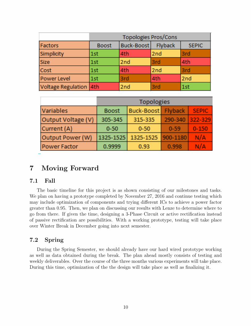
The second stage of PFC design is the DC/DC conversion. In most applications ofDC/DC converters, the input is a clean DC wave. In our case, the input is a pulsating DCwaveform ranging from 0 to 170V. This means that we are forced to use a larger inductorand capacitor in order to maintain a clean and consistent output waveform regardless ofwhich topology is used. With that in mind, the boost, buck-boost, flyback and SEPICwere chosen to further investigate. With each topology, we looked at the pros and cons aswell as the waveforms to compare the results and ultimately decide on which topology tofocus our efforts into. By looking at the strengths in simplicity, size, cost, power level, andvoltage regulation of the various topologies, the Boost Converter was determined to be themost appropriate. Team 1703 and Lenze have decided to continue forward with the BoostConverter design and implement it in between the AC/DC rectification circuit and the VFDinput.
4.4 Control
The third stage of the PFC circuit is the control circuit. This is the most complex part ofthe circuit due to the range of options for control. The three major options are analog control,designing and building our own feedback circuit using a microcontroller, and a prebuilt ICchip. Each of these options have their own advantages and disadvantages. Analog controlexcels in its speed, and cost effectivity. Despite that, analog control falls short in stabilityover a range of conditions and adjustability. Another option is designing and building afeedback circuit using a microcontroller. This option excels in its adjustability as we couldoptimize it specifically to each application. Where this option falls short is cost, complexityand development time. The last option is using a pre-built IC control chip. This optionexcels in cost, stability, and size. The only downfalls of this are the dependence upon a 3rdparty chip, which Lenze has no problems with given that they have other products that relyon 3rd party chips, and that we are limited on adjustability. The PFC Control chip thatwe have in mind, Infineon (ICE3PCS01G) is less than $2.00 per chip and has been testedat power levels very similar to ours. This chip allows adjustability of output voltage andswitching frequency from 21kHz to 250kHz.
6

4.5 Budget
Lenze has stated the budget to be $2000 which is very lenient. Additionally, since we areplanning on the boost topology, further costs are minimized as boost is the simplest topologyof the four we investigated. Lenze has stated that they will purchase parts and PCBs.
5 Experimental Procedures
5.1 Power Factor Measurement
In simulation, we measure power factor using a voltage and a current probe to determinereal and reactive power and use those to calculate power factor. With hardware, we will usea power meter that measures the input voltage and input current and computes the real,apparent, and reactive power, and displays the power factor.
5.2 Power Efficiency
In order to calculate efficiency of the converter, we will use a power meter on the inputand output of the circuit and compare them using the following equation:
5.3 Total Harmonic Distortion(THD)
In simulation, we measure THD using a Spectrum Analyzer. With hardware, we will usean oscilloscope.
7

6 Preliminary Results
6.1 Buck-Boost
6.2 SEPIC
8

6.3 Flyback
6.4 Boost
9
7 Moving Forward
7.1 Fall
The basic timeline for this project is as shown consisting of our milestones and tasks.We plan on having a prototype completed by November 27, 2016 and continue testing whichmay include optimization of components and trying different ICs to achieve a power factorgreater than 0.95. Then, we plan on discussing our results with Lenze to determine where togo from there. If given the time, designing a 3-Phase Circuit or active rectification insteadof passive rectification are possibilities. With a working prototype, testing will take placeover Winter Break in December going into next semester.
7.2 Spring
During the Spring Semester, we should already have our hard wired prototype workingas well as data obtained during the break. The plan ahead mostly consists of testing andweekly deliverables. Over the course of the three months various experiments will take place.During this time, optimization of the the design will take place as well as finalizing it.
10

8 Conclusion
This project is focusing on designing a PFC circuit for Lenze that would work with one oftheir variable frequency drives. Working with a 120VAC input we must design a circuit thatcan output 325VDC and a power factor of 0.95 or greater. Looking at various topologiesbased on their size, simplicity, power level and voltage regulations, the boost converter wasthe most suitable for the design. Using the Simulink software in MATLAB we obtained somepreliminary results for all the converters. Moving forward, we plan to work with the PFCcontrol chip (ICE3PCS01G) by Infineon to complete our closed loop control. Additionallylooking to the future, we expect to have a working prototype by the November and starttesting moving into next semester. As an extra goal, we plan on looking into a three-phasedesign as that is much more optimal versus single phase due to industy demand.
11

9 Personnel and Collaborators
Ethan HotchkissSenior Engineering [email protected]
Kevin WongSenior Engineering [email protected]
Paul GlazeSenior Engineering [email protected]
Jethro BaliaoSenior Engineering [email protected]
Program Manager: Christopher [email protected]
Faculty Advisor: Ali [email protected]
University of ConnecticutStorrs, CT 06269
Lenze Americas CorporationUxbridge, MA 01569
12

References
[1] H. Wei, and I. Batarseh. Comparison of Basic Converter Topologies For Power Factor Correction 1998.
[2] J.W. Kolar and T. Friedli. The Essence of Three-Phase PFC Rectifier Systems-Part I. IEEE Transactionson Power Electronics, Vol. 28, No.1,pp176-198.
[3] S. Abdel-Rahman, F. Stuckler, K. Siu. PFC boost converter design guide. 2016.
[4] P.T. Krein. Elements of Power Electronics 2nd Edition. 2015.
13