POWER AMPLIFIERS - UCSB · 2016-03-27 · Power Amplifiers • Purpose of a power amplifier...
84
POWER AMPLIFIERS ©James Buckwalter 1
Transcript of POWER AMPLIFIERS - UCSB · 2016-03-27 · Power Amplifiers • Purpose of a power amplifier...

POWER AMPLIFIERS
©James Buckwalter 1

Power Amplifiers
• Purpose of a power amplifier– Generate high output power
– Efficient conversion of DC power to RF power
– Linear amplification
• Generally PAs will be – Common source
– Cascode
• Inductor is a “choke” to provide DC
• Capacitor is a “ac coupling” path to output
©James Buckwalter 2

Definition of Power
• Instantaneous Power
• Average Power
• There is a component that averages to zero that corresponds to energy stored and dissipated each cycle.
©James Buckwalter 3
P = v t( ) × i t( )
Pav =1
Tv t( ) × i t( )dt
t=0
T
ò

Definition of Power
• If the voltage and current is
• The average power becomes
• In phasor notation
©James Buckwalter 4
v t( ) =V cos wt( )
i t( ) = I cos wt +q( )
Pav =1
TVI cosq cos2 wt( )dt
t=0
T
ò =1
2VI cosq
v t( ) =V Re e jwt{ }
P =1
2Re vi*{ } =
1
2V
2Re Y{ } =
1
2I
2Re Z{ } Preac =
1
2Im vi*{ }

Example:
©James Buckwalter 5

Time Scales for Power Amplifiers
• Carrier T ~1ns, Period Ts ~100ns, Control ~ 1ms
©James Buckwalter 6

Power Scales for Power Amplifiers
©James Buckwalter 7

Large Signal Analysis
• Consider harmonic analysis
• Power
• In phasor
©James Buckwalter 8
P =V0I0 +1
2Vk Ik cos qk( )
k³1
å
v t( ) = Vk cos kwt( )k³0
å
i t( ) = Ik cos kwt +qk( )k³0
å
P =1
2Vk
2
k³1
å Re Yk{ } =1
2Ik
2
k³1
å Re Zk{ }

Harmonic Engineering
• Power is not simply V2
• May see strong harmonic content but power delivered at harmonics might be small due to impedance at harmonics
• Keep load reactive at harmonics.
©James Buckwalter 9
P =1
2Vk
2
k³1
å Re Yk{ } =1
2Ik
2
k³1
å Re Zk{ }
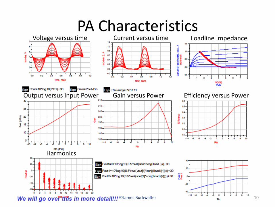
PA Characteristics
©James Buckwalter 10
Voltage versus time Current versus time Loadline Impedance
Output versus Input Power Gain versus Power Efficiency versus Power
Harmonics

Notation
• Be careful about notation of voltage, current, and power.
• Average power
• For small signal, RMS voltage and current is common
• Therefore,
©James Buckwalter 11
vrms =v
2
P =1
2Re vi*{ }
P = Re vrmsi*
rms{ }

Units
• Peak Units
• RMS Units
v
RF= v
pksin w
RFt( )
vrms
=1
Tv
RFt( )( )
2
dt-T /2
T /2
ò
© James Buckwalter 12

What does it mean to be “matched”?
• The antenna will appear to be 50 at the RF frequency so the input impedance of the receiver should be 50 .
• Why 50 ?
– It’s historical but an important (IEEE) standard.
– 30 Ohms offers the best power handling.
– 75 Ohms offers the lowest attenuation.
– All test interfaces are 50 .
©James Buckwalter 13

Power Amplifier Matching
• Loadline should be matched to 50 Ohm antenna output (or something like that).
• How do we do this?
©James Buckwalter 14

Power Delivered to a Load
Pdel ,L
=1
2Â v
LiL
*{ } =1
2Â i
LZ
LiL
*{ } =iL
2
2R
L
Pdel ,L
=v
S
2
2
RL
RS+ R
L( )2
+ XS+ X
L( )2
©James Buckwalter 15

Power Delivered to a Load
©James Buckwalter 16
Pdel ,L
=v
S
2
2
RL
RS+ R
L( )2
+ XS+ X
L( )2
• How do you maximize the power delivered?
• Vary the load while keeping the source impedance fixed.

Two Important Conclusions:Conjugate (Power) Matching
I)XS
= -XL
II)¶P
DL
¶RL
= 0® RS
= RL
Pdel ,L,max
=v
S
2
8RS
=v
L
2
2RL
©James Buckwalter 17
since vL
=R
L
RS+ R
L
vS
=1
2v
S

What is the Penalty for Mismatch?
©James Buckwalter 18
Pdel ,L
=v
S
2
8RS
1
1+d X
2RS
æ
èç
ö
ø÷
2®
Pdel ,L
Pav ,S
=1
1+d X
2RS
æ
èç
ö
ø÷
2
X
S= -X
L+dX
• The PA is very nonlinear at high power. This explains how the gain and power change under different conditions.

Characteristics of Transistor Amplifiers
©James Buckwalter 19

Ideal Assumptions
• The transistor acts like a current source
• Current controlled by input voltage as long as threshold condition is satisfied.
• Current is independent of output voltage as long as minimum/maximum output voltage is satisfied.
©James Buckwalter 20

Difference between Current Models
©James Buckwalter 21

Classes of Power Amplifier
• Bias point amplifiers
– Class-A
– Class-B
– Class-C
• Switching amplifier
– Class-E
– Class-F
©James Buckwalter 22

PA Waveform
• Drain current consists of DC current and AC current
©James Buckwalter
iD = ID + id
id = ipk sin wot( )
vo = -id R
23

PA Quiescent Conditions
• DC Conditions
VDS = VDD
IDS = IDD
• DC and AC Conditions
VDS = VDD+VAC
VAC = VOUT
IDS = IDD+IAC
IAC=-ILOAD=-VOUT/RL
©James Buckwalter 24

Transistors as Power Devices
• At high-power, the transistor is operating as a large signal device.
• Large voltage swing across drain-source junction
• Maximum voltage is VMAX~2Vddof transistor
• Minimum voltage is VMIN ~Vkwhere transistor begins to turn off
• Maximum current of transistor at VMIN is Imax
©James Buckwalter 25

Time Waveforms
©James Buckwalter 26
vin =VGG + vpk cos wot( )
iD = IDD - ipk cos wot( ) = IDD - iL
iL = ipk cos wot( )
vDS =VDD + iL RL

Class A Operation
• Bias such that device never turns “off” (Vgs – Vt > 0)
• Note that the peak voltage across transistor is 2 Vdd!
©James Buckwalter
iD
= IDD
- ipk
cos wRF
t( )
v
DS=V
DD+ i
pkR
Lcos w
RFt( )
P
RF=
ipk
2 RL
2
27

Class-A Efficiency
• How much power consumption is required to keep the amplifier from turning off?
• Device power
• Maximum efficiency
©James Buckwalter
h =P
RF
PDC
=i
pk
2 RL
2IDD
VDD
£V
DD
2VDD
= 50%
IDD
³ ipk
VDD
³ ipk
RL+V
MIN
28
iD
= IDD
- ipk
cos wRF
t( )v
DS=V
DD+ i
pkR
Lcos w
RFt( )
P
dev= P
devdc( )+ P
devw( ) = I
DDV
DD-
1
2i
pk
2 RL

Voltage Swing Limitations
• Efficiency
• RF Voltage/Current
• This defines the limitation in delivering power
©James Buckwalter 29
h =P
o
PDC
=P
o
Pmax
Pmax
PDC
VRF ,MAX
=1
2V
MAX-V
MIN( )
VDD
=1
2V
MAX+V
MIN( )
VMAX
= 2VDD
-VMIN
IRF ,MAX
= IDD
PRF ,MAX
=1
2V
RF ,MAXI
RF ,MAX=
1
4V
MAX-V
MIN( ) IDD
PDC
=VDD
IDD

Class-A Efficiency vs RF Power
• Construct efficiency in terms of minimum device output voltage and d.c. voltage
©James Buckwalter 30
h =P
RF
PDC
=P
RF
PRF ,MAX
PRF ,MAX
PDC
h =P
RF
PRF ,MAX
1
2
VMAX
-VMIN( ) I
DD
VMAX
+VMIN( ) I
DD
h =P
RF
PRF ,MAX
1
2
2VDD
- 2VMIN
2VDD
=P
RF
PRF ,MAX
1
21-
VMIN
VDD
æ
èçç
ö
ø÷÷
Operating Power
Maximum Class-A Efficiency
Device FactorBack-off of amplifier
results in linear efficiency degradation with power
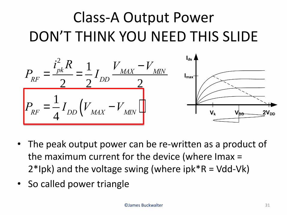
Class-A Output PowerDON’T THINK YOU NEED THIS SLIDE
• The peak output power can be re-written as a product of the maximum current for the device (where Imax = 2*Ipk) and the voltage swing (where ipk*R = Vdd-Vk)
• So called power triangle
©James Buckwalter 31
PRF
=i
pk
2 R
2=
1
2I
DD
VMAX
-VMIN
2
PRF
=1
4I
DDV
MAX-V
MIN( )

Power Triangle
• Another way to look at this is that the area under the IV curve should give the total power
©James Buckwalter 32
PRF
=1
2
IMAX
2
VMAX
-VMIN( )
2
PRF
=1
8I
MAX2V
DD-V
MIN( )Breakdown voltage (BV) may be larger than twice the VDD. More generally, we should take 2 VDD

Class A Load-line Resistance
• Must increase current handling or voltage handling of device.
• Load line is defined by
• For Silicon CMOS, voltage is extremely limited. Large current means wide transistors and low output impedances.
©James Buckwalter
RLL
=V
MAX-V
MIN( )I
MAX
33

Example: 1 W Power Amplifier in CMOS
• You are asked to design a 1 W PA in a 1 V CMOS process.
• What is the size of the transistor assuming that the transistor can handle 1 mA per micron of DC current; i.e. 2mA per micron of Idd? The knee voltage is 0.3 V.
• What is the loadline resistance?
©James Buckwalter 34

Solution: 1 W Power Amplifier in CMOS
• Power delivered from PA:
• CMOS PAs handle high current!!!
©James Buckwalter
PDEL
=I
DD2V
DD-V
K( )4
IDD
=4P
DEL
2VDD
-VK
=4W
1.7V= 2.35A
35

Solution: 1 W Power Amplifier in CMOS
• The loadline resistance is
• This is an extremely small resistance. This makes matching difficult as we will discuss today!
©James Buckwalter
RLL
=V
MAX-V
K( )I
DC
=2.7V
2.35A=1.14W
36

More Examples
©James Buckwalter 37

Class A Load-line Resistance
• Load line can be defined under different conditions
• Different load lines selected for fixed Vdd
©James Buckwalter 38
P
RF=
1
8I
MAXV
MAX-V
MIN( )
h =P
RF
PRF ,MAX
1
21-
VMIN
VDD
æ
èçç
ö
ø÷÷

Power/Efficiency Trade-off
• Changing RL changes efficiency and output power.
• Larger loadlineresistance achieves higher efficiency at expense of power.
©James Buckwalter 39
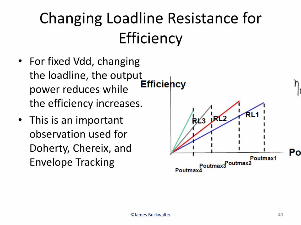
Changing Loadline Resistance for Efficiency
• For fixed Vdd, changing the loadline, the output power reduces while the efficiency increases.
• This is an important observation used for Doherty, Chereix, and Envelope Tracking
©James Buckwalter 40

CLOSER LOOK AT LOADLINE
©James Buckwalter 41

Effect of Output Capacitance
• Loadline is not static when transistor model is no longer quasi static
©James Buckwalter 42
iD
= IDD
- ipk
cos wRF
t( )+CDS
d
dtv
OUT
id
= -ipk
cos wRF
t( )+ jwRF
CDS
vOUT

Matching Conditions
• 1) DC loadline considerations dictate choice of RL to optimize Pout or PAE combination. (not necessarily gain)
• 2) Imaginary part of load admittance is established to match the imaginary part of device
©James Buckwalter 43
BL = -Á YO{ }

Simulating the Reactive Loadline
• De-embed the Cds and Cdg values and add these as “negative” capacitors to get a quasi-static loadline.
©James Buckwalter 44

Simulation of Waveforms
• Now we can look inside transistor to get loadline
©James Buckwalter 45

Load Pull Contour
• Load pull measurement (simulation) consists of systematically varying load impedance and measuring amplifier characteristics
• Load pull contours describe how Pout (efficiency, linearity, etc) vary with ZL
©James Buckwalter 46

Load Pull Contours
©James Buckwalter 47

Differences in Load Pull for Power and PAE
©James Buckwalter 48

PA Design Methodology
1. Choose Vdd based on transistor technology with sufficient power handling capability and breakdown voltage
2. Using DC characteristics choose load line and verify the Pout can be obtained.
3. Determine the input impedance matching network using the bias condition on the average DC current corresponding to average output power
4. Determine the load susceptance and match the output to obtain RL and BL
5. Provide output match at harmonic frequencies6. Set-up bias network7. Optimize using simulator.
©James Buckwalter 49

Overdriven Class A
• You might wonder what happens when we turn a class A amplifier to “11”
• In general, you get higher output power and efficiency in the overdriven regime but this is difficult to analyze
• Vin determine Idrain through the nonlinear transistor characteristics
• Vdrain depends on the load impedance at different harmonics
• If Vdrain is too low, the transistor is forced into triodand becomes a voltage source causing current collapse.
©James Buckwalter 50

©James Buckwalter 51

Power Added Efficiency
• Power added efficiency incorporates the RF power lost into driving the device.
• The PAE is never more than the drain efficiency.
• High gain is required from the PAE to make the amplifier efficient.
©James Buckwalter
, , , ,
,
1
11
rf out rf in rf out rf in
DC DC rf out
P P P PPAE
P P P
PAEG
52

PAE
• Gain can be changing with output power as device is pushed into compression
©James Buckwalter 53
Po
=i
pk
2 R
2=
gmv
in( )2
2R
G =P
o
Pin
µ gm
2 R

CLASS B
©James Buckwalter 54

Class-B Operation
• Drain current on for half the cycle
©James Buckwalter
iD
=i
pkcos w
ot( ) i
d> 0
0 id
£ 0
ì
íï
îï
vpk
= -iD
2Rcos w
RFt( )
P
RF=
vpk
2
2R£
VDD
2
2R
55
Note that the current is half-wave rectified by the voltage is a sine wave!

Fourier Components for Half-Wave
• Even harmonics result from half wave current
©James Buckwalter 56
iD
=i
pkcos w
ot( ) i
d> 0
0 id
£ 0
ì
íï
îï
iD
f( ) =i
pk
p+
ipk
2sin 2p ft( ) -
2ipk
p
cos 4pkft( )4k 2 -1k³1
å
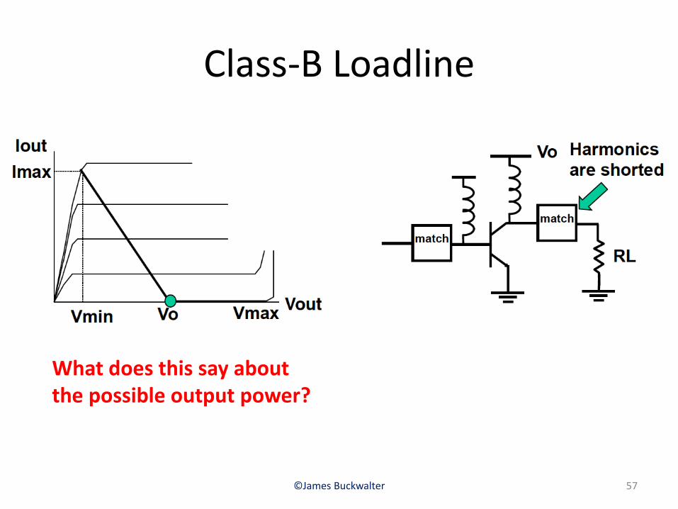
Class-B Loadline
©James Buckwalter 57
What does this say about the possible output power?

Harmonic Matching for Class-B
©James Buckwalter 58
• At fundamental, generate loadline match
• At higher harmonics, ZL = 0

Power Dissipation in Class A and Class B
©James Buckwalter 59

Class-B Current Analysis
• IQ should be zero for DC (no power consumption with no input).
• However, quiescent current is obviously not the “average” current.
• To calculate the d.c. power consumption, the d.c. average power
• Looking at the half-wave drain current, we could also calculate
©James Buckwalter 60
IDC
=1
2piPK
sin q( ) dq £iPK
p0
p
ò
IFUND
=1
piPK
sin2 q( ) dq £iPK
20
p
ò

Class-B Efficiency
• The output power and DC power are
• Therefore, the maximum drain efficiency is
©James Buckwalter
h =P
RF
PDC
=
vPK
2
2RV
DDiPK
p
=p
2
vPK
2
RVDD
iPK
=p
4
vPK
VDD
®hMAX
= 78%
61
PRF
=1
2v
PKiPK
=1
2
vPK
2
R=
1
2R
iPK
2
æ
èçç
ö
ø÷÷
2
PDC
=VDD
IDC
=VDD
iPK
p

Class-A versus Class-B
• Comparing power of Class-A and B
• Comparing efficiency of Class-A and B
• What is the cost of class-B amplifier?
©James Buckwalter
PRF ,A
=V
DD
2
2RP
RF ,B=
VDD
2
2R
50% 78%A B
62

Class-B Efficiency Revisited• How does efficiency depend on knee voltage?
• The efficiency depends on the output power
• The drain efficiency changes with the root of the output power. Recall for class-A!
©James Buckwalter 63
h =p
4
VRF ,MAX
VDD
VRF
VRF ,MAX
=p
4
VMAX
-VMIN
VMAX
+VMIN
PRF
PRF ,max
h =p
41-
VMIN
VDD
æ
èçç
ö
ø÷÷
PRF
PRF ,max
h =1
21-
VMIN
VDD
æ
èçç
ö
ø÷÷
PRF
PRF ,MAX

Efficiency vs. Power
©James Buckwalter 64
Very important! Note that not only is the peak power higher the efficiency is higher in backoff.
When the average power is 3 dB lower than the peak, what is the efficiency for class-A and class-B?

Class-B Loadline
©James Buckwalter 65
How do we match to this loadline?

Class-B Loadline
©James Buckwalter 66
• The piecewise loadline shown in the previous slides seems to suggest a loadline.
• However, we should consider the loadlinebased on the fundamental. Therefore, the voltage swing at the fundamental is (Vmax –Vmin )/2. The current swing is Imax/2.
• The loadline resistance is the same as class-A!
RL =Vmax -Vmin
Imax

Maximum Output Power for Class-B
• Again, this is the same as class-A output power
• So what is the penalty?
©James Buckwalter 67
PRF
=1
2v
RF ,MAXiRF ,MAX
PRF
=1
8V
MAX-V
MIN( ) IMAX

Gain for Class-B
• Compared to the gain for Class-A amplifier the power gain of class-B is ¼ (or 6 dB) less.
• What is the implication of this? Lower PAE!
©James Buckwalter 68
P
RF=
ipk
2 R
8=
gmv
in( )2
8R

Gain
©James Buckwalter 69

Features of Class-B
©James Buckwalter 70

CLASS C
©James Buckwalter 71

Class-C Amplifier
©James Buckwalter 72
• Like class-B, IQ= 0
• Unlike class-B, conduction
angle < 180 deg
• Gain is low since device is
turned on for only a short
period
Iout
VoutVoVmin
Imax
Vmax
time
time
Vo
Vce
Idc
Ic
Vrf
match
match
VoRL
Harmonics are
shorted

Class-C Amplifier
©James Buckwalter 73
• IDC < IRF / p
• PRF < 1/4 VRF IRF
• PDC = VDD IDC
Iout
VOUTVDDVMIN
Imax
VMAX
time
time
VDD
Vds
IDC
Id
VRF
match
match
VoRL
Harmonics are
shorted

Load Impedance Is A Resonant Network
©James Buckwalter 74
RLmatch
Vo
fo
Z=RL at fo
Z=0 at 2fo, 3fo, 4fo,…
Short at all harmonics here
Z
10 WAt fo -j2W j2W
10 WAt 2fo -j1W j4W
Representative Z values
fo
2fo

Class-C Waveform
©James Buckwalter 75
timeIdc
Ic
I t( ) =iPK cosf - IS when iPKcosf > IS
0 otherwise
ìíï
îï
cosf =IS
iPK
®IS is the (negative) offset
iPK is the amplitude
IDC =1
2pI q( )
0
f
ò dq =1
2piPK cosq - IDD( )
0
f
ò dq
IDC =1
piPK sinf - IDDf( )
IFUND =1
pI q( )
0
2p
ò cosqdq =2
pI q( )
0
f
ò cosqdq
IFUND =2
piPK cos2 q - IS cosq( )dq
0
f
ò
IFUND =2
p
1
2iPKf +
1
4iPK sin2f - IS sinf
æ
èç
ö
ø÷
IFUND =2
piPK
1
2f +
1
4sin2f - cosf sinf
æ
èç
ö
ø÷
IFUND =iPK
pf -
1
2sin2f
æ
èç
ö
ø÷

Class-C Conduction
• Note the angle φ defined for the waveform analysis is related to the conduction angle of the transistor by a factor of two, i.e. 2φ=Φ
• Φ is the conduction angle during which the current conducts through the transistor. What happens for Φ of pi or 2pi?
©James Buckwalter 76
IFUND =iPK
p
F
2-
1
2sinF
æ
èç
ö
ø÷IDC =
iPK
psin
F
2-
F
2cos
F
2
æ
èç
ö
ø÷

Class-C Efficiency
• As conduction angle approaches 0, the efficiency approaches 100%.
• What is the penalty?
©James Buckwalter
h =P
RF ,MAX
PDC
=v
PKiPK
2VDD
IDC
=F- sin F( )( )
2 2sinF
2
æ
èç
ö
ø÷-Fcos
F
2
æ
èç
ö
ø÷
æ
èç
ö
ø÷
77

Class C Waveform Analysis
• Calculate efficiency in presence of
©James Buckwalter 78
h =1
2
vPKiPK
VDC IDC
=1
2
vpk
VDC
ipk
pipk
p
F - sin F( )
2sinF
2
æ
èç
ö
ø÷-Fcos
F
2
æ
èç
ö
ø÷
=Vpk
VRF ,MAX
VRF ,MAX
VDC
f F( )
h =VFUND
VFUND,MAX
VFUND,MAX
VDC
f F( )
h = f F( ) 1-VMIN
VDD
æ
èç
ö
ø÷
POUT
POUT ,MAX
f 0( ) =1 f p( ) =p
4f 2p( ) =
1
2
f F( ) =1
2
F- sin F( )
2sinF
2
æ
èç
ö
ø÷-Fcos
F
2
æ
èç
ö
ø÷

Power Amplifier Comparison
©James Buckwalter 79

Class-C Amplifier Efficiency
• Class C has very good efficiency because whenever the
device has current, Vds is particularly low
©James Buckwalter 80
time
time
Vo
Vds
Idc
ID
Vrf

Class-C Waveform Analysis
• How about the loadlineresistance?
©James Buckwalter 81
RL =VFUND
IFUND
VFUND =VMAX -VMIN
2
IFUND = IS
F
2-
1
2sinF
æ
èç
ö
ø÷
IMAX = IS - IO = IS 1- cosF
2
æ
èç
ö
ø÷
IFUND =IS
p
F
2-
1
2sinF
æ
èç
ö
ø÷ =
IMAX
2p
F - sinF
1- cosF
2
RL = pVMAX -VMIN
IMAX
2 1- cosF
2
æ
èç
ö
ø÷
F - sinF
0
2
4
6
8
10
12
14
16
18
20
0 15 30 45 60 75 90
Theta (degrees)
RL
/ R
L C
lass A
Iout
VoutVoVmin
Imax
Vmax

Gain and Conduction Angle
©James Buckwalter 82
Pin (dBm)
Gain (dB)
6dB
Class A
Class B ideal
Class B real
Class AB "ideal"
Class AB "real"
Class C "real"

Power Amplifier Comparison
©James Buckwalter 83
• Maximum voltage swing is 2Vo – Vmin
• Gain is 6 dB lower for class-B than class-A, expect it to be even lower than class-C.
• Power density is the same for class A and B but lower for class C.

Other Classes of Amplifiers
• PA research is focused around getting high-power power at high-efficiency.
• Class D Amplifiers– Push-pull style amplifier
• Class E/F Amplifiers– Switching amplifiers which can allow 100% PAE
but require care with harmonics
• Class J Amplifier– Overdriven class-A
©James Buckwalter 84