Power Amplifier devices for UMTS - ARMMS · Power Amplifier devices for UMTS A D Vare, R Hopper ......
8
Power Amplifier devices for UMTS A D Vare, R Hopper Roke Manor Research, Romsey, Hants S051 OZN, [email protected] , [email protected] When developing power amplifiers for use in UMTS basestations it is vital to make the right choice for the final power device(s). This paper outlines the impact of the 3GPP specification for base stations on the power amplifier, determines tests and benchmarks to enable device comparison, and discusses how device characteristics can influence the rest of the system. INTRODUCTION The power amplifier stage of a typical cellular basestation represents a high proportion of the overall unit cost, this in part is due to the high cost of the power transistor used to generate the final output power, therefore a key decision for the designer is: `how many transistors?' too few and the spectral requi rements will not be met, too many and the efficiency will suffer and the cost will be excessive, this is true regardless of any linearity enhancement scheme surrounding the amplifier power stages. The other key question that must be answered is: `What technology will achieve the required goals?' here the usual choice is between LDMOS and GaAsFET, and can only be answered by device testing against a common benchmark. This paper attempts to: • Detail the requirements of the power device based on the 3GPP specification. • Derive a test suite for characterising devices to enable common comparison. • Detail device demoboards and test boards. • Present typical results. • Discuss results and draw conclusions that impact the overall architecture. REQUIREMENTS The bottom line for the spectral requirements of a UMTS basestation is detailed in (1) from this the requirements for the power amplifier must be drawn, and then finally given knowledge of the performance of any linearity enhancement scheme employed, the requirements for the power stage. Within the 3GPP specification there are 4 power output classes defined ranging from > 43dBm total power output down to < 31dBm. These power classes modify the spectrum emission mask that the basestation must comply with. So to make the first key decision one must determine how much power the power transistor(s) need to generate. First, the basestation power output must be decided. Second, knowledge of all losses following the final transistor(s) must be known, and third, how much improvement does the linearity enhancement scheme give. It is assumed here that all 3GPP compliant power amplifiers will employ a linearity enhancement scheme, because unfortunately transistors are not yet linear enough on their own, although there is hope with techniques like `Derivative Super-position' (2)(3) and other potentially more linear structures like GaN. Typical linearity enhancement schemes used today include feedforward and digital pre-distortion. Not all the above questions can be answered at the start of a project; therefore all devices short-listed must be tested over a range of output powers. CHARACTERISATION To make an informed decision as to the correct number and type of devices, one must gather data for all devices that might be suitable. The first port of call is the manufacturer datasheet; these vary a lot in quality and can really give the designer a hard time as quite often each manufacturer uses tests that do not cover your particular requirements. This has historically been very true of datasheets for UMTS transistors for several reasons; (a) the 3GPP standard has been around for a several years and has only recently been frozen, thus parameters change, (b) test equipment manufacturers have done their best to keep up with the standards but inevitably there has been a lag, thus different test equipment give different results, (c) the specification gives several options for the modulation, for example when measuring spurious emissions there is a choice of three formats depending on what the basestation will support, which can affect the measured performance. So inevitably this means that the designer must determine a set of tests, which will provide all the information necessary to make the final decision. Datasheet information usually includes the following information that is useful to the designer: • Single carrier Adjacent Channel Leakage Ratio (ACLR) versus output power. © 22 October 2002 Roke Manor Research Ltd 4/1
Transcript of Power Amplifier devices for UMTS - ARMMS · Power Amplifier devices for UMTS A D Vare, R Hopper ......
Power Amplifier devices for UMTS
A D Vare, R Hopper
Roke Manor Research, Romsey, Hants S051 OZN, [email protected] , [email protected]
When developing power amplifiers for use in UMTS basestations it is vital to make the right choice for the final powerdevice(s). This paper outlines the impact of the 3GPP specification for base stations on the power amplifier, determines
tests and benchmarks to enable device comparison, and discusses how device characteristics can influence the rest of thesystem.
INTRODUCTIONThe power amplifier stage of a typical cellularbasestation represents a high proportion of the overallunit cost, this in part is due to the high cost of the powertransistor used to generate the final output power,therefore a key decision for the designer is: `how manytransistors?' too few and the spectral requi rements willnot be met, too many and the efficiency will suffer andthe cost will be excessive, this is true regardless of anylinearity enhancement scheme surrounding the amplifierpower stages. The other key question that must beanswered is: `What technology will achieve the requiredgoals?' here the usual choice is between LDMOS andGaAsFET, and can only be answered by device testingagainst a common benchmark.This paper attempts to:
• Detail the requirements of the power devicebased on the 3GPP specification.
• Derive a test suite for characterising devices toenable common comparison.
• Detail device demoboards and test boards.• Present typical results.• Discuss results and draw conclusions that
impact the overall architecture.
REQUIREMENTSThe bottom line for the spectral requirements of a UMTSbasestation is detailed in (1) from this the requirementsfor the power amplifier must be drawn, and then finallygiven knowledge of the performance of any linearityenhancement scheme employed, the requirements for thepower stage. Within the 3GPP specification there are 4power output classes defined ranging from > 43dBm totalpower output down to < 31dBm. These power classesmodify the spectrum emission mask that the basestationmust comply with.So to make the first key decision one must determinehow much power the power transistor(s) need togenerate. First, the basestation power output must bedecided. Second, knowledge of all losses following the
final transistor(s) must be known, and third, how muchimprovement does the linearity enhancement schemegive. It is assumed here that all 3GPP compliant poweramplifiers will employ a linearity enhancement scheme,because unfortunately transistors are not yet linearenough on their own, although there is hope withtechniques like `Derivative Super-position' (2)(3) andother potentially more linear structures like GaN.Typical linearity enhancement schemes used todayinclude feedforward and digital pre-distortion.Not all the above questions can be answered at the startof a project; therefore all devices short-listed must betested over a range of output powers.
CHARACTERISATIONTo make an informed decision as to the correct numberand type of devices, one must gather data for all devicesthat might be suitable. The first port of call is themanufacturer datasheet; these vary a lot in quality andcan really give the designer a hard time as quite ofteneach manufacturer uses tests that do not cover yourparticular requirements. This has historically been verytrue of datasheets for UMTS transistors for severalreasons; (a) the 3GPP standard has been around for aseveral years and has only recently been frozen, thusparameters change, (b) test equipment manufacturershave done their best to keep up with the standards butinevitably there has been a lag, thus different testequipment give different results, (c) the specificationgives several options for the modulation, for examplewhen measuring spurious emissions there is a choice ofthree formats depending on what the basestation willsupport, which can affect the measured performance.So inevitably this means that the designer must determinea set of tests, which will provide all the informationnecessary to make the final decision.
Datasheet information usually includes the followinginformation that is useful to the designer:
• Single carrier Adjacent Channel Leakage Ratio(ACLR) versus output power.
© 22 October 2002 Roke Manor Research Ltd
4/1
• Two carrier ACLR and 3'd OrderIntel-modulation Distortion (IMD) versus outputpower.
• Optimised source and load impedances (usefulfor the test circuit).
However quite often the modulation used for themeasurements is not fully described in terms of statistics,or varies between manufacturers, or worse still, not evenstated, necessitating re-measurement to a commonstandard. In some cases the designer may have a specialmodulation employing clipping algorithms, which wouldhave to be used.In addition to the above data, the designer would alsowant to characterise the following parameters using a testcircuit or demoboard:
• S parameters over frequency.• Gain and phase compression.• 2 carrier CW IMD products, 3 `d , 5 `h , and 7`h at
least.• Sensitivity to variation in Idq.
To make these measurements repeatable and to removethe drudgery it is essential to automate the process asmuch as possible. At RMRL a suite of programs havebeen written using Agilent VEE, which has enabled adatabase of over 300MB to be generated for a broadspectrum of parts.As well as spectral, (1) also contains other requirementsthat relate to the wanted signal modulation quality,namely Error Vector Magnitude (EVM), and Peak CodeDomain Error (PCDE), both defined in section 6.7 of (1).These requirements are very important as they relate tothe overall bit error rate for the base station transmitter.The power amplifier will contribute to the overall figuresof EVM and PCDE, but measurements have shown thatif the power amplifier meets the spectral requirementsthen the linearity is sufficiently good such that thecontribution to signal modulation quality will benegligible. Therefore swept measurements of EVM andPCDE versus power output do not necessarily need to beincluded in the test suite.
W-CDMA TEST SIGNALWithin the 3GPP specification, there are options as to themodulation format, these are referred to as `test models'.
There are basically 4 different test models, each used forspecific tests, in the case of ACLR and spuriousemissions the relevant test model is Test Model 1,defined in (1) 6.1.1.1. However within this test modelthere are 3 options; 16, 32 and 64 DPCH (DedicatedPhysical CHannel) or `users', this results in a spreadspectrum signal which exhibits a high peak to mean ratiodependant on the option chosen. Figure 1 plots thetheoretical Complementary Cumulative Density Function(CCDF) for each option. It shows that there is about 1dBdifference in absolute peak power between each option.This can affect the test results, therefore for repeatabilityreasons, one option should be standardised on. At RMRL
the 64 DPCH has been decided on as this stresses thetransistor to the maximum.In most base stations a clipping algorithm is employed inDSP at the baseband stage to reduce the maximum peakof the signal in order to reduce the stress on the poweramplifier, allowing it to provide more power and hencebetter efficiency. However when choosing devices it isbetter to consider testing using an unclipped waveformsince this represents a worse case scenario. Resultsshould only improve with clipping. It adds a safetymargin for the designer, and provides protection fromchanges to the actual clipping algorithm.
Figure 1: Test Model 1/64 CCDF cuove
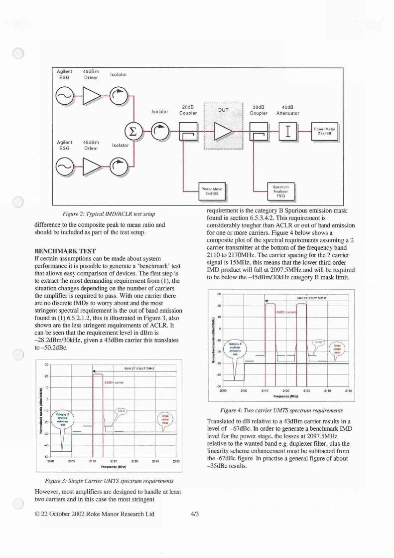
TEST BENCHFor testing high power devices a special test setup isrequired comprising:
• A high power dc supply.• 2 x W-CDMA capable signal generators, e.g.
Agilent ESG or Rohde and Schwarz SMIQ.• 2 x High power class A driver amplifiers.• Isolators.• High power directional couplers.• High power attenuators.• 2 x power meters.• High dynamic range spectrum analyser with rms
detector and ACLR measuring capability e.g.Rohde and Schwarz FSIQ.
A typical test setup is given in Figure 2 below:Note that the two tone signal is generated by combiningat high power, and note the use of isolators, bothmeasures ensure that source IMD is negligible. Thewhole test set-up must be carefully calibrated for losswith a network analyser to ensure accurate measurementssince a loss of 0.2dB already represents 1W in 20W.Note also that (1) 6.1.1.6.3 states that each modulatedcarrier shall have a different scrambling code,incremented from 0 starting with the lowest carrierfrequency, there shall also be 1/5 time slot offset betweentheir frame structures. This again will make a minor
© 22 October 2002 Roke Manor Research Ltd
4/2
0Agilent
45dBmESG
DriverIsolator
Agilent
45dBmESG
DriverIsolator
Isolator20dB
Coupler30dB
40dBCoupler
Attenuator
Power MeterE4418B
SpectrumAnalyser
FS IQ
0
4/3
Figure 2: Typical IMD/ACLR test setup
difference to the composite peak to mean ratio andshould be included as part of the test setup.
BENCHMARK TESTIf certain assumptions can be made about systemperformance it is possible to generate a `benchmark' testthat allows easy comparison of devices. The fast step isto extract the most demanding requirement from (1), thesituation changes depending on the number of carriersthe amplifier is required to pass. With one carrier thereare no discrete IlViDs to worry about and the moststringent spectral requirement is the out of band emissionfound in (1) 6.5.2.1.2, this is illustrated in Figure 3, alsoshown are the less stringent requirements of ACLR. Itcan be seen that the requirement level in dBm is-28.2dBm/30kHz, given a 43dBm carrier this translatesto -50.2dBc.
30 --
-
_ __
_ ...
i.
_.. -1-Band 21101o 2170M-lz
420
43dBrr carnet10
0
10 RCLAE -E Gleamy B
((
)5^-
.
-20 l , ' muskM1
{I--L
-
40
502090
2100
2110
2120
2130 2140
2150Frequency (MHz)
Figure 3: Single Carrier UMTS spectrum requirements
However, most amplifiers are designed to handle at leasttwo carriers and in this case the most stringent
© 22 October 2002 Roke Manor Research Ltd
requirement is the category B Spurious emission maskfound in section 6.5.3.4.2. This requirement isconsiderably tougher than ACLR or out of band emissionfor one or more carriers. Figure 4 below shows acomposite plot of the spectral requirements assuming a 2carrier transmitter at the bottom of the frequency band2110 to 2170MHz. The carrier spacing for the 2 carriersignal is 15MHz, this means that the lower third orderIMD product will fall at 2097.5MHz and will be requiredto be below the -45dBm/30kHz category B mask limit.
30Band 2110 to 2170NHz
20
10i43d8m career
1
o
^
>
- 10 -
QlgOry B 1 ACLR
-i^ snya
-20 t e,n̂ I / ,kimlEx
-40
-502080
2100
2110
2120
2130
2140
2150Frequency (MHz)
Figure 4: Two carrier UMTS spectrum requirements
Translated to dB relative to a 43dBm carrier results in alevel of -67dBc. In order to generate a benchmark IMDlevel for the power stage, the losses at 2097.5MHzrelative to the wanted band e.g. duplexer filter, plus thelinearity scheme enhancement must be subtracted fromthe -67dBc figure. In practise a general figure of about-35dBc results.

TWO CARRIER BENCHMARK:Total 3GPP requirement =
-67dBcLinearity improvement scheme = 20dBDuplexer out of band loss*=
10dBMargin =
2dBPower stage IMD level =
-35dBc
* K&L WSD-00189 UMTS duplexer
The linearisation improvement figure of 20dB suggeststhat a feedforward system is requi red to produce acompliant multi-carrier amplifier.
DEMOBOARDS AND TEST BOARDSThe quickest route to characterising a device is to obtainan application demoboard from the transistormanufacturer. The demoboards are designed to be asflexible as possible and adjustable tuning elements areoften included for optimisation. The user can thereforeoptimise the demoboard to some degree for theirparticular application. However it is necessary at somepoint to make your own board customised to yourapplication and manufacturing philosophy.Sometimes the delivery of a demoboard is either outsideof your timescales or simply not available, in this case itis necessary to make your own board from the outset.Designing your own test board for a high powertransistor is at lust a rather slow process as there aresignificantly more steps involved compared to say asmall signal device, in particular with regard to themechanical and heatsinldng arrangements. The typicaltasks involved include the following:
• If gerber files for a test board can be obtainedfrom the manufacturer, use them!
• No gerber files, then hopefully obtain themanufacturer declared optimum source and loadimpedances, decide what they mean and usethem as a starting point for matching circuits.
• Design the test board including bias networks.• Design the heatsink and / or baseplate.• Have all parts manufactured.• Build the pcbs and assemble the completed test
board onto the heatsink.• Test the test board, and tune up if necessary.• Compare the results against the datasheet.
Figure 5 is an example of a test board for a MotorolaMRF 21125 based on manufacturer supplied data, it ispart of a family of test boards all designed around thesame heat sinking and biasing arrangements in order tospeed up development of a test board for a new device. Itcan be seen that the gate and drain circuitry can berapidly removed and replaced in order to experiment withdifferent matching circuits. The gate bias circuit is alsoon a separate board for the same reason, however this is
only a temporary solution as the gate bias circuit shouldreally be thermally connected to the power transistor inorder for the transistor Idq to be correctly thermallycompensated. Note also that the power transistor is notsoldered, this is only acceptable for a test board, wheredevices are to be compared, soldering makes this hardwork.
Figure 5: Typical power device testboard
TYPICAL CHARACTERISATION RESULTS
Figure 6 below shows small signal gain curves over afrequency sweep of 500MHz centered on 2140MHz. Itcompares a typical demoboard against another transistorof the same family optimised for flat gain. Flat gain isimportant for manufacture repeatability as a `peaked'response is more sensitive to component tolerances.
18IuMTB
Band16
4
^ ^nnS 12
'
cr)
10
CI) I 1 ? nnr...6
-Typical demoboard
-Bandwidth optimised2
design
0
1.89
2.14
2.39
Frequency (MHz)
Figure 6: Small Signal Gain
Flat gain (and phase) over frequency is also a veryimportant characteristic when linearisation is employed.In the case of a feedforward system the amplitude (and
© 22 October 2002 Roke Manor Research Ltd
4/4

Where A is the amplitude ripple in dB, and 4 is the phaseripple, both over the bandwidth of interest. Taking thetwo devices above over a bandwidth of 15MHz, and60MHz, and the following cancellation figures resultassuming the phase ripple for both devices were equal tozero:
DeviceCarrier spacing Standard
demoboardOptimised
device15MHz -33.70dB -64.80dB60MHz -25.76dB -38.48dB
Compared to the 2 carrier benchmark described earlierwhere 20dB is required from the lineariser, the standarddemoboard would cause severe limitations as carrierspacing is increased as on its own would consume nearlyall the budget just due to gain ripple. The figures will beworse if phase ripple were included. The output stageconsidered here will be only one part of the completeamplifier line-up and the way the S21 of all the devicesinteract would have to be carefully considered.
Figure 7 below shows a typical plot of power gain andphase versus input power level. The amplifiercompression at the higher power levels can be clearlyseen.
Figure 7: CW power sweep
The absolute gain and shape of the compression curve isrelated to the quiescent current (Idq) of the transistorwhich for a class AB stage will be in the region of 10%of Id max. It is important to set the optimum Idq for bestefficiency and linearity. Linearity is strongly affected byIdq due to the gain peaks as the device approachessaturation, these cause so called IMD `sweet spots', the
gain peaks are a form of build-in pre-distortion giving alittle gain expansion. The gain response can also interactwith the phase curve to give the same result. If thetransistor manufacturer had better control of the devicetransconductance curve then maybe we might seeimproved transistors and the goal of a class AB amplifierwithout an external lineariser might be achievable.It is still useful to plot the gain and phase of a transistorversus power level, but is not ideal for optimisinglinearity, it is far better to adjust Idq whilst observingIMD directly.
As mentioned above Idq has a strong effect on thelinearity of a device, this can be easily observed in Figure8 which shows 3'd order IMD levels versus averagepower output from a typical LDMOS device as Idq isvaried. For this particular device the optimum Idq underCW excitation is about 1.30A. Similar plots could bedrawn for 5th and 7th order products, however generally3rd order is dominant and so optimising Idq for this orderis normally adequate. Note for this device the dip in IMDor `sweet spot' at 40dBm output level at an Idq of 1.3A.
Characterisation using CW is very useful for carrying outan initial comparison of devices and optimisation,however the performance will change considerably underW-CDMA excitation due to the high peak to mean ratioand spread spectrum characteristics of the signal. Figure9 shows ACLR versus output power for the same deviceas shown in Figure 8. By comparison the followingpoints can be drawn:
• At high power s45dBm, the IMD/ACLR levelsare similar and the amplifier is driven well intocompression by the peaks of the signal.
• With W-CDMA the `sweet spots' havedisappeared.
• Significant `memory effect' or ACLR imbalanceis evidence with W-CDMA as power is backedoff.
• At high Idq where the device is getting closer toclass A bias, the back off curve with W-CDMAretains the shape seen with CW, albeit at anoverall lower level.
• The optimum Idq setting for single car rier W-CDMA has increased to =1.6A.
I
I
I
I
J -40
-Ma g (dB) - -45
--Phase (deg) - -50
-55
-60
-s5
-70
-75
-80
-85
-so
10
15
20
25
30
35
40
45
Input power (dBm)
19
18
17
16
12
11
10
9
S:=10. 1og[ 10 10/ +1-410 01.cos(1, ),
phase) ripple limits the amount of improvement that canbe obtained over a given bandwidth.The amount of improvement or cancellation is given theequation below found in (4):
A
© 22 October 2002 Roke Manor Research Ltd
4/5

-+3rd imd 0.70A-+3rd imd 1.OOA
-+3rd imd 1.30Aimd 1.60A-+3rd
3rd- -
--3rd
- - - --3rd imd-3rd imd-3rd imd
-Efficiency-Efficiency
imdimd
0.70A1.00A1.30A1.60A1.9A
1.0A1.6A
+3rd imd 1.90A- -Efficiency 0.7A
Efficiency 1.3A_
Efficiency 1.9A
AdMallr
25
30
35
40
45
50
Average output power (dBm)
80
70
60u -20
50 Z.U T.. -30
40 `2v -40
30 W 0-50
20
10 -60
0 -70
imd 0.70A-+3rd 3rd imd 0.70A 3rd imd 1.OOA
-3rd imd 1.30A 3rd imd 1.60A
-3rd imd 1.9A- - -Efficiency 1.0A- - -Efficiency 1.6A
-imd 1.OOA-+3rd
+3rd imd 1.30Aimd 1.60A- +3rd
-imd 1.90A-+3rd
- -Efficiency 0.7AEfficiency 1.3AEfficiency 1.9A
-
30
35
40
Average output power (dBm)
-10
-60
-70
0
70
60
20
10
-8020 20
0
80
25
0
45
50 g'
u40 m
30 W
Figure 8: CW IMD versus Idq
Figure 9: ACLR with 1 x W-CDMA source
ACLR with a spread signal is really a composite of 3 `d ,5th 7`h etc orders of IMD products added together overthe complete range of baseband frequencies, or like aclosely spaced multi-tone CW signal, thus it is nosurprise that the plots seen in Figure 8 and Figure 9 areso different.
Now consider the case of a two can•ier W-CDMA signalapplied to the same amplifier, see Figure 10 and Figure11 below.In Figure 10 the plot of 3rd order IMD it can be seen thatthe `sweet spots' have reappeared, but there is significant`memory effect' with more than 10dB IMD imbalancenoted at some power levels. This points to poor design ofthis particular demoboard supplied as is from themanufacturer.
Figure 10: IMD with 2 x W-CDMA source
Here we see:• `Sweet spots' very sensitive to Idq.• Large memory effect.• Optimum Idq now = 1.9A (at 2 carrier
benchmark -35dBc).
Figure 11: ACLR (lower carrier) with 2 x W-CDMA source
Figure 11 shows the ACLR plot for the same 2 carrierW-CDMA input signal, but just considering the lower ofthe two carriers, in practise the other carrier will exhibitessentially the same set of curves. The plots aresignificantly different to the single carrier case shown inFigure 9, however with two carriers the absolute peak tomean ratio will have been modified to perhaps 12dB sothis is no surprise.Here we conclude:
• ACLR with two carriers is significantly lower inlevel compared to 3rd order IMD (5dB or moreat high power), therefore less important.Normally improving the 3rd order IMD to meetspecification will automatically ensure ACLR isacceptable.
• Optimum Idq is again = 1.9A.
-10
+ACLR 0.70A
- --ACLR 0.70A+ACLR 1.OOA ACLR 1.OOA+ACLR 1.30A
-ACLR 1.30A+ACLR 1.60A ACLR 1.60A+ACLR 1.90A
-ACLR 1.9AEfficiency 0.7A
-Efficiency 1.0AEfficiency 1.3A
-Efficiency 1.6AEfficiency 1.9A
-70
-80 -20
-10
-20
80
70
60
+ACLR 0.70A
--ACLR 0.70A
---+ACLR 1.OOA ACLR 1.OOA-10 -
+ACLR 1.30A
-ACLR 1.30A
-+ACLR 1.60A ACLR 1.60A
-+ACLR 1.90A
-ACLR 1.9A
- -Efficiency 0.7A
- - -Efficiency 1.0A
Efficiency 1.3A
- - -Efficiency 1.6AEfficiency 1.9A
70
60
80
© 22 October 2002 Roke Manor Research Ltd
4/6
IMPACT OF MEMORY EFFECT
As observed Figure 10, this particular demoboardexhibited quite different memory effects under 2 carrierCW conditions compared to 2 carrier W-CDMAconditions: in the CW case hardly any memory wasobserved and in the W-CDMA case up to a very poor10dB was noticed.If 10dB IMD imbalance exists at the benchmark levelthen the implications are that if the higher of the twoIMDs is enhanced by the memory effect whilst the otheris cancelled then the amplifier is not providing the powerit could if there were no memory effect. This means thatwith a feedforward amplifier either the correction has towork harder or the amplifier has to be backed off morewith the hit on efficiency. Neither case is desirable.Memory effect can also cause big problems with digitalpre-distorting linearisers as independent coefficients tocontrol each IMD product is not available and thus oneIMD could be improved at the expense of the other, orjust a generally poorer performance results. Morerecently digital techniques at RMRL have beendeveloped to overcome these limitations. Therefore it isimportant for multicarrier amplifiers that the memoryeffect be characterised.Memory effect can be explained in different ways, oneuseful way described by Steve Cripps in (5) is "a time lag...between AM-AM and AM-PM responses", this can beintroduced by poor gate and drain decoupling at lowfrequencies causing a distortion of the envelope currentswhich results in IMD asymmetry. This is really onlyapplicable to reduced conduction angle amplifiers likeclass AB where drain current varies with output power,this is seen in the plots above and note that as Idq israised towards class A bias, memory effects reduces.The 2 carrier CW IMD plot does not show up thememory effect very well because the carrier spacing usedwas only 1MHz. Better evidence will be seen if thecarrier spacing is varied between 1MHz and about15MHz which represents more closely the range ofenvelope frequencies with a 2 carrier W-CDMA signal.Figure 12 below shows a typical family of curvesmeasured with a carrier spacing varied between 1 and15MHz, here large amounts of IMD imbalance areobserved as the carrier spacing is varied.
Figure 12: 3rd Order CW IMD versus output power with 1 to15MHz carrier spacings
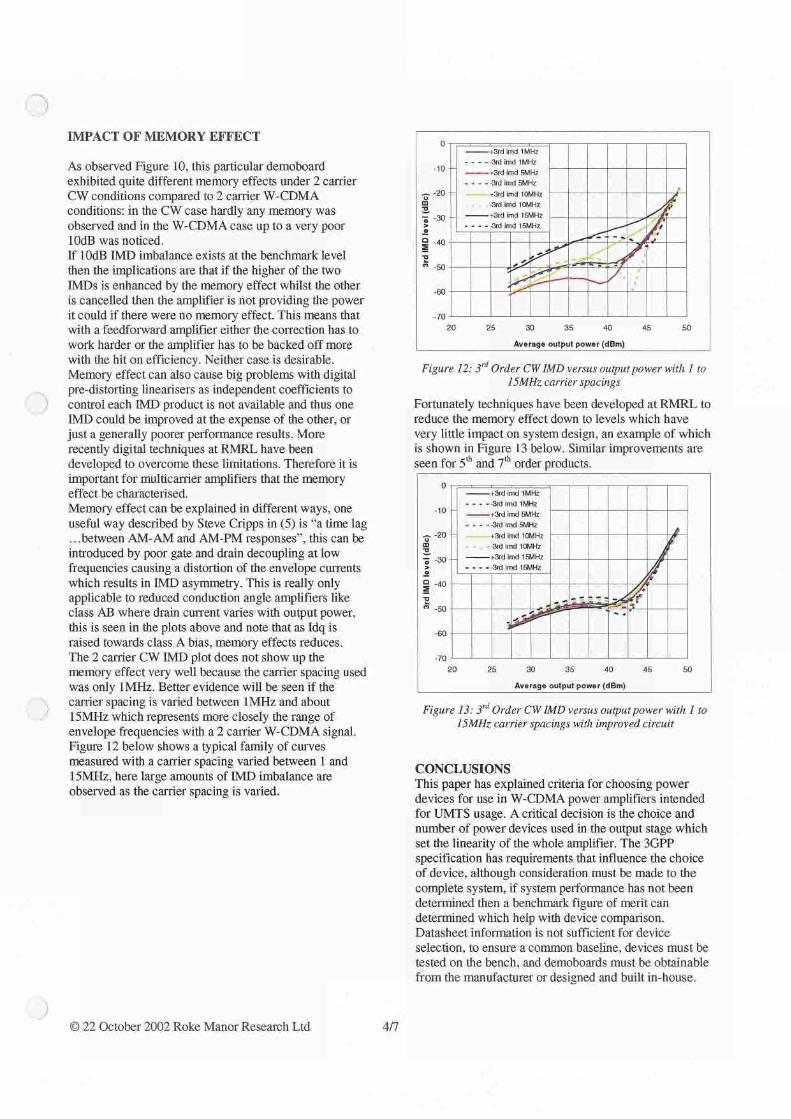
Fortunately techniques have been developed at RMRL toreduce the memory effect down to levels which havevery little impact on system design, an example of whichis shown in Figure 13 below. Similar improvements areseen for 5`h and 7`h order products.
Figure 13: 3rd Order CW IMD versus output power with 1 to15MHz carrier spacings with improved circuit
CONCLUSIONSThis paper has explained criteria for choosing powerdevices for use in W-CDMA power amplifiers intendedfor UMTS usage. A critical decision is the choice andnumber of power devices used in the output stage whichset the linearity of the whole amplifier. The 3GPPspecification has requirements that influence the choiceof device, although consideration must be made to thecomplete system, if system performance has not beendetermined then a benchmark figure of merit candetermined which help with device comparison.Datasheet information is not sufficient for deviceselection, to ensure a common baseline, devices must betested on the bench, and demoboards must be obtainablefrom the manufacturer or designed and built in-house.
-+3rd md 1MHz 3rd imd 1MHz-+3rd md 5MHz 3rd imd 5MHz
_--
- - -
-3rd+3rd imd
+3rd imd
-3rd imd
imd 10MHz15MHz
15MHz
z
,''A
20
25
30
35
40
45
50
Average output power (dBm)
0
-1o
-60
-70
Average output power (dBm)
-+3rd md 1MHz 3rd imd 1MHz-+3rd imd 5MHz
- --3rd md 5MHz+3rd md 10MHz-3rd imd 10MHz
_ - +3rd imd 15MHz 3rd imd 15MHz
.
.=
T.
-7020 25 30
35
40 5045
0
-10
u -20Ma
m -30
O -40
co -5o
-60
© 22 October 2002 Roke Manor Research Ltd
4/7
Careful considerations must be made to the test setup toensure that the correct test signals are used with thecorrect test equipment and that the system is accuratelycalibrated.It is important to build up an automated test suite to carryout the tests to ensure repeatability and gather more datathan could be achieved manually.Traditional characterisation using CW stimulus althoughuseful is not sufficient for complete characterisation of adevice, measurements must made using W-CDMAsources and swept over power.Memory effects in class AB devices limit performanceand reduce efficiency. There are very significantdifferences between the performance of devices withinthe same technology and between different technologies,this too must be carefully characterised. Techniques areavailable to minimise the impact of device memory.
ACKNOWLEDGEMENT
RMRL would like to acknowledge the support ofSIEMENS ICM and for their permission to publish thispaper.
The authors would like to thank contributions fromA.Altham and M.Horgan both of RMRL to this paper.
REFERENCES
(1)
3GPP TS 25.141 V5.1.0(2001-12), 3rd GenerationPartners/tip Project; Technical specification Group RadioAccess Networks; Base Station conformance testing (FDD)(Release 5).
(2) `Application of Derivative Superposition to low-IM3Distortion IF Amplifiers", Workshop on RF CircuitTechnology, A CMP Europe Conference, University ArmsHotel, Cambridge, UK. March 11 "', 2002. Peter M. Jupp (RokeManor Research), D.R. Webster (University College London).
(3) Ultra-Linear Distributed Class-AB LDMOS RFPower Amplifier for Base Stations, M.P. van der Heijens, H.C.de Graaff, L.C.N. de Vreede, J.R. Gajadharsing, and J.N.Burghatz. IEEE 2001.
(4) Feedforward Linear Power Amplifiers, NickPothecary, Artech House 1999.
(5) Advanced Techniques in RF Power Amplifier Design,Steve C. Cripps, Artech House 2002.
© 22 October 2002 Roke Manor Research Ltd
4/8