Polymer integrated Young interferometers for label-free...
78
UNIVERSITATIS OULUENSIS ACTA C TECHNICA OULU 2012 C 432 Meng Wang POLYMER INTEGRATED YOUNG INTERFEROMETERS FOR LABEL-FREE BIOSENSING APPLICATIONS UNIVERSITY OF OULU GRADUATE SCHOOL; UNIVERSITY OF OULU, FACULTY OF TECHNOLOGY, DEPARTMENT OF ELECTRICAL ENGINEERING; UNIVERSITY OF OULU, INFOTECH OULU C 432 ACTA Meng Wang
Transcript of Polymer integrated Young interferometers for label-free...
ABCDEFG
UNIVERS ITY OF OULU P.O.B . 7500 F I -90014 UNIVERS ITY OF OULU F INLAND
A C T A U N I V E R S I T A T I S O U L U E N S I S
S E R I E S E D I T O R S
SCIENTIAE RERUM NATURALIUM
HUMANIORA
TECHNICA
MEDICA
SCIENTIAE RERUM SOCIALIUM
SCRIPTA ACADEMICA
OECONOMICA
EDITOR IN CHIEF
PUBLICATIONS EDITOR
Senior Assistant Jorma Arhippainen
University Lecturer Santeri Palviainen
Professor Hannu Heusala
Professor Olli Vuolteenaho
University Lecturer Hannu Heikkinen
Director Sinikka Eskelinen
Professor Jari Juga
Professor Olli Vuolteenaho
Publications Editor Kirsti Nurkkala
ISBN 978-951-42-9963-6 (Paperback)ISBN 978-951-42-9964-3 (PDF)ISSN 0355-3213 (Print)ISSN 1796-2226 (Online)
U N I V E R S I TAT I S O U L U E N S I SACTAC
TECHNICA
U N I V E R S I TAT I S O U L U E N S I SACTAC
TECHNICA
OULU 2012
C 432
Meng Wang
POLYMER INTEGRATED YOUNG INTERFEROMETERS FOR LABEL-FREE BIOSENSING APPLICATIONS
UNIVERSITY OF OULU GRADUATE SCHOOL;UNIVERSITY OF OULU,FACULTY OF TECHNOLOGY,DEPARTMENT OF ELECTRICAL ENGINEERING;UNIVERSITY OF OULU,INFOTECH OULU
C 432
ACTA
Meng W
ang
C432etukansi.fm Page 1 Friday, October 26, 2012 12:55 PM

A C T A U N I V E R S I T A T I S O U L U E N S I SC Te c h n i c a 4 3 2
MENG WANG
POLYMER INTEGRATED YOUNG INTERFEROMETERS FOR LABEL-FREE BIOSENSING APPLICATIONS
Academic dissertation to be presented with the assentof the Doctoral Training Committee of Technologyand Natural Sciences of the University of Oulu forpublic defence in Auditorium TS101, Linnanmaa, on 23November 2012, at 12 noon
UNIVERSITY OF OULU, OULU 2012

Copyright © 2012Acta Univ. Oul. C 432, 2012
Supervised byProfessor Risto MyllyläDocent Jussi Hiltunen
Reviewed byProfessor Seppo HonkanenProfessor Janis Spigulis
ISBN 978-951-42-9963-6 (Paperback)ISBN 978-951-42-9964-3 (PDF)
ISSN 0355-3213 (Printed)ISSN 1796-2226 (Online)
Cover DesignRaimo Ahonen
JUVENES PRINTTAMPERE 2012
Wang, Meng, Polymer integrated Young interferometers for label-free biosensingapplications. University of Oulu Graduate School; University of Oulu, Faculty of Technology, Department ofElectrical Engineering; Infotech Oulu, P.O. Box 4500, FI-90014 University of Oulu, FinlandActa Univ. Oul. C 432, 2012Oulu, Finland
Abstract
Integrated optical (IO) sensor allowing sensitive, label-free, real-time and multi-parametermonitoring of bio-molecular interactions are conventionally fabricated with inorganic dielectricsinherited from CMOS manufacturing technology. Polymers as complement materials to inorganicdielectrics are becoming to have an increasing market share for IO circuits in opticalcommunications networks owing to its good optical properties, versatile processibility and lowcost. This work aims at developing disposable low-cost biosensors based mainly on polymericmaterials, with a performance comparable to inorganic-dielectric based IO biosensors.
This thesis describes the development of polymer IO biosensors based on the Younginterferometer (YI) transducer platform for ambient noise compensation and a complete periodicintensity fringe pattern. Three different waveguide configurations were utilized, taking intoconsideration operational simplicity, fabrication simplicity and enhanced sensitivity. Among thedeveloped polymer biosensors, an unconventional interferometer structure: a vertically placeddual-slab waveguide interferometer and an inverted rib waveguide configuration were employed.To enhance the sensitivity of the waveguides, deposition of Ta2O5 high index coating wasperformed on the rib waveguide configuration. Along with the development of polymer biosensorsbased on the inverted-rib waveguide configuration, a fabrication process was also developedfeaturing UV-imprinting and spin coating. The simple two-step fabrication process demonstratedusing a polymer mold is potentially transferable to the roll-to-roll manufacture process.
Calibration of the developed sensors was performed by homogeneous refractive index (RI)sensing with glucose de-ionized water solutions. By investigating an antibody – antigen bindinginteraction involving C-reactive protein and its conjugates, this thesis confirmed the applicabilityof the developed sensors to specific molecule detection. Moreover, to establish the influence ofwater molecular absorption on measurement stability, an evaluation was carried out on thepolymeric waveguide. Finally, the thesis presented a comparison between the developed sensors,exploring their sensitivities, stabilities, limits of detection (LODs) and other aspects related tooperation and fabrication. The results indicated that the Ta2O5-coated polymer waveguide sensorhad a high sensing capability. In homogeneous RI sensing, the achieved detection limits were9×10-7 RIU (refractive index unit), i.e., three times the noise level, and 270 fg/mm2 for surfacemass density.
Keywords: immunoassay, optical biosensor, rib waveguide, slab waveguide, Ta2O5high-index coating, UV-imprinting, UV-sensitive polymer, Young interferometer

Wang, Meng, Polymeeriset integroidun optiikan Youngin interferometritmerkkiaineettomissa biomittauksissa. Oulun yliopiston tutkijakoulu; Oulun yliopisto, Teknillinen tiedekunta, Sähkötekniikan osasto;Infotech Oulu, PL 4500, 90014 Oulun yliopistoActa Univ. Oul. C 432, 2012Oulu
Tiivistelmä
Integroidulla optiikalla toteutetut anturit mahdollistavat biomolekulaarisen vuorovaikutuksentutkimisen käyttäen herkkiä moniparametrisia ja merkkiaineettomia menetelmiä. Näiden bioan-tureiden valmistukseen käytetään tavallisesti CMOS-teknologian piiristä tuttuja epäorgaanisiapuolijohteita ja eristemateriaaleja. Viime aikoina on kuitenkin polymeeristen materiaalien käyt-töä integroidussa optiikassa tutkittu merkittävästi johtuen polymeerien hyvistä optisista ominai-suuksista, monipuolisesta työstettävyydestä ja edullisista kustannuksista. Tämän työn tarkoituk-sena on kehittää edullisia, kertakäyttöisiä, pääasiallisesti polymeerisistä materiaaleista valmistet-tuja bioantureita, jotka vastaavat suorituskyvyltään epäorgaanisista materiaaleista valmistettujaintegroidun optiikan antureita.
Tässä työssä kehitetyt polymeeriset integroidun optiikan bioanturit perustuvat Youngin inter-ferometriin mahdollistaen ympäristökohinan kompensoinnin ja ne tuottavat pintavuorovaikutus-ten tutkimiseen jaksoittaisen interferenssikuvion. Työssä hyödynnettiin kolmea erilaista valoka-navarakennetta huomioiden niiden käytön helppous, valmistuksen yksinkertaisuus ja mittaus-herkkyys. Yksi kehitetyistä polymeerisistä bioantureista koostui päällekkäisistä kerrostetuistapolymeerikerroksista. Toisen tutkitun rakenteen toiminta puolestaan perustui käänteiseen harjan-nevalokanavaan. Mittausherkkyyttä parannettiin pinnoittamalla polymeerirakenne Ta2O5-pin-noitteella. Näin muodostui kerrostettu komposiittivalokanava, joka oli tässä työssä tutkittu kol-mas sensorirakenne. Itse bioanturien lisäksi kehitettiin myös valmistusprosessi, jossa hyödynnet-tiin UV-painatusta ja nestefaasipinnoitusta. Tässä työssä havaittiin lisäksi, että kehitetty yksin-kertainen valmistusmenetelmä on paitsi toimiva, myös mahdollisesti siirrettävissä rullalta rullal-le valmistus- ja tuotantoteknologiaan.
Kehitettyjen anturien kalibrointi suoritettiin homogeenisella taitekerroinmittauksella käyttä-en liuoksia, jotka valmistettiin glukoosista ja deionisoidusta vedestä. Kehitettyjen anturiensoveltuvuus spesifien molekyylien tunnistamista varten todennettiin tutkimalla vasta-aineiden jaantigeenien sitoutumisreaktioita ja vuorovaikutusta C-reaktiivisella proteiinilla ja sen konjugaa-teilla. Lisäksi työssä tutkittiin veden absorption vaikutusta mittauksen stabiilisuuteen. Tutkimuk-sessa suoritettiin vertailu kehitettyjen anturien ja niiden ominaisuuksien välillä kiinnittäen huo-miota mittausherkkyyteen, stabiilisuuteen, määritys- ja toteamisrajoihin ja muihin anturien val-mistukseen sekä käyttöön liittyviin keskeisiin piirteisiin. Tulokset osoittavat, että Ta2O5-pinnoi-tetun polymeerivalokanavan mittausherkkyys oli suurin vertailluista rakenteista. Homogeenises-sä taitekerroinmittauksessa saavutettu määritys- ja toteamisraja oli 9×10⁻⁷ taitekerroinyksikköä(RIU). Pintamassatiheysmittauksessa saavuttu tulos oli 270 fg/mm2.
Asiasanat: harjannevalokanava, immunomääritys, optinen bioanturi, planaarinenvalokanava, Ta2O5-pinnoitus, UV-painatus, UV-sensitiivinen polymeeri, Younginterferometri

7
Acknowledgements
This study is based on research work carried out at the Optoelectronics and
Measurement Techniques Laboratory of University of Oulu during the years
2007–2012. Therefore I would like to express my deepest gratitude to my
supervisor Prof. Risto Myllylä for providing me the research opportunity in his
group, and all the support and guidance throughout my undergraduate and
doctoral studies.
My sincere appreciation goes to Dr. Jussi Hiltunen from VTT Technical
Research Center of Finland. I want to thank him for leading me to his research
expertise, and for sharing his time, knowledge and ideas to guide me through the
difficulties of research. Thanks also to other colleagues from VTT, Dr. Leena
Hakalahti for her help of providing many of the facilities and resource necessary
to carry out my research work, Dr. Pentti Karioja, M.Sc. Sanna Uusitalo, M.Sc.
Christina Liedert, M.Sc. Marianne Hiltunen, and M.Sc Noriyuki Masuda for their
help and fruitful discussions.
I want to acknowledge and thank all my colleagues in the Optoelectronics
and Measurement Techniques Laboratory, especially Dr. Hanna Jobbour, Lic.Tech.
Eija Vieri, M.Sc. Karoliina Jokinen, and M.Sc. Miia Määttälä for helping me
accomplish this thesis work with their friendship, encouragement, and continuous
support.
I wish to thank co-author Prof. Jyrki Lappalainen, M.Sc. Jarkko Puustinen in
Microelectronics and Materials Physics Laboratory for AFM measurements, and
Dr. Martin Charlton and Dr. Stuart Pearce for preparing Ta2O5 coating in
University of Southampton.
I would also like to thank Prof. Seppo Honkanen (University of Eastern
Finland) and Prof. Janis Spigulis (University of Latvia) for reviewing my thesis.
I want to thank my parents for believing in me and supporting me to pursue
my degrees in Finland ten years ago. Without their encouragement, none of this
would be possible. Finally, I owe my deepest and loving gratitude to my beloved
husband Dr. Wu Chen and son Jiayuan Chen. Without their love and
understanding, I would have never finished this book.
Financial support from Infotech Oulu Graduate School, TaunoTönning
Foundation, and Tekniikan edistämissäätiö (TES) is highly appreciated.
Oulu, June 2012 Meng Wang

8
9
Abbreviations and symbols
1D one dimensioanl
2D two dimensional
AFM atomic force microscopy
BSA bovine serum albumin
CMOS complementary-symmetry metal–oxide–semiconductor
CRP C-reactive protein
CTE coefficient of thermal expansion
CVD chemical vapor deposition
DI de-ionized
FFT fast Fourier transform
F13 –TCS tridecafluoro-(1,1,2,2)-tetrahydrooctyl-trichlorosilane
III-V refers to the periodic table classification; material composition of
group three and five materials
IgG immunoglobulin G
IO integrated optics
KCl potassium chloride
LOD limit of detection
NaCl sodium chloride
Na2HPO4 disodium hydrogen phosphate
NaH2PO4 sodium dihydrogen phosphate
NIL nano-imprinting lithography
PBS phosphate-buffered saline
PDMS polydimethylsiloxane
PMMA poly(methyl methacrylate)
RI refractive index
RIE reactive ion etching
RIU refractive index unit
RMS root-mean-square
SEM scanning electron microscope
Si silicon
Si3N4 silicon nitride
SiO2 silicon dioxide
SiON silicon oxynitride
SNR signal-to-noise-ratio
SOI silicon on insulator

10
SPR surface plasma resonance
Ta2O5 Tantalum pentoxide
TiO2 Titanium dioxide
TE transverse electric
TIR total internal reflection
TM transverse magnetic
UV ultraviolet
YI Young interferometer
a half width of the waveguide
arb. unit arbitrary unit
°C degrees Celcius
b half length of the waveguide
D the distance from the sensor output facet to the collecting objective
lens
d the separation between the sensing and referencing waveguide at the
output facet
dn/dc the refractive index increment of the protein solution
Da Dalton, 1.66×10⁻²⁷ kg
fg/mm2 femtogram per square millimeter
E electric field
E|| tangential part of the electric field
H|| tangential part of the magnetic field
I, I1, I2 Intensity
j imaginary unit
k0 wave number in vacuum
kx, ky wave number in the x- and y-direction
L interaction length
ml milliliter
nad refractive index of the adlayer
nc refractive index of the cover medium
neff effective refractive index
nf refractive index of the core
nm nanometer
nM nanomolar
ns refractive index of the substrate
P spatial period of the fringe pattern

11
pol polarization
p, q integers corresponding to the numbers of the optical power peaks in
x- and y- directions
rad radian
rpm rounds per minute
s second
t time
tad thickness of the adlayer
teff effective waveguide thickness
tf thickness of the waveguide
x, y, z Cartesian coordinates
β propagation constant
Γ coupling efficiency
δ phase change of the propagating wave in the sensing waveguide
ΔC concentration change of the analyte
ΔM change of the surface mass density
Δneff change of effective refractive index
ΔX change of one or a combination of parameters
Δφ phase difference between the referencing and sensing waveguides
Δzf, c evanescent field penetration depth into the substrate (j=s) or cover
medium (j=c)
λ wavelength
µm micrometer
ρ parameter used for theoretical sensitivity calculation
ω angular frequency

12
13
List of original papers
I Wang M, Uusitalo S, Määttälä M, Myllylä R & Känsäkoski M (2008) Integrated dual-slab waveguide interferometer for glucose concentration detection in the physiological range. Proc SPIE 7003: 70031N-1-10. DOI: 10.1117/12.780184.
II Wang M, Uusitalo S, Liedert C, Hiltunen J, Hakalahti L & Myllylä R (2012) Polymeric dual-slab waveguide interferometer for biochemical sensing applications. Appl Opt 51: 1886–1893.
III Wang M, Hiltunen J, Uusitalo S, Puustinen J, Lappalainen J, Karioja P & Myllylä R (2011) Fabrication of optical inverted-rib waveguides using UV-imprinting. Microeletron Eng 88(2): 175–178.
IV Wang M, Hiltunen J, Liedert C, Hakalahti L & Myllylä R (2012) An integrated Young interferometer based on UV-imprinted polymer waveguides for label-free biosensing applications. J Europ. Opt Soc Rap Public 7: 12019.
V Wang M, Hiltunen J, Liedert C, Pearce S, Charlton M, Hakalahti L, Karioja P & Myllylä R (2012) Highly sensitive biosensor based on UV-imprinted layered polymeric–inorganic composite waveguides. Opt Express 20: 20309–20317.
Author’s contribution to publications I-V:
I The author studied the slab waveguide Young interferometer with the
commercialized SiON based sensor chip provided by Farfield Scienctific
Inc. In this paper, a theoretical sensitivity analysis of three-layer waveguide
biosensors was carried out together with co-author Sanna Uusitalo.
II The author fabricated and characterized the polymer dual-slab waveguide
interferometer biosensors with glucose water solutions and demonstrated
the functionality of biosensing with non-specific adsorption of
biomolecules.
III Together with co-author Dr. Jussi Hiltunen, the author developed the
fabrication process for the inverted-rib polymer waveguide. The author
fabricated the waveguides utilizing UV-imprinting lithography.
Characterization of the waveguide was done together with Dr. Jussi
Hiltunen. Fabrication of the inverted-rib waveguide is a fundamental step
for development of sensing systems in Papers IV & V.
IV The author fabricated and characterized the polymer inverted-rib
waveguide Young interferometer biosensor. The sensor was calibrated with
bulk refractive index sensing using glucose water solutions. Biosensing
ability was demonstrated with specific antibody-antigen binding.
14
V The composite polymeric-inorganic waveguide interferometer biosensor
was developed, based on the structure of the polymer inverted-rib
waveguide prepared by the author. Ta2O5 high-index coating was fabricated
by co-author Jussi Hiltunen at Southampton University. The author
conducted both the theoretical and experimental sensitivity analysis and
performed the biosensing measurements using an immunoassay provided
by co-author Christina Liedert. The measurement results suggested a
significant enhancement of sensitivity and detection limit.

15
Contents
Abstract Tiivistelmä Acknowledgements 7 Abbreviations and symbols 9 List of original papers 13 Contents 15 1 Introduction 17
1.1 Basics of optical biosensors .................................................................... 17 1.2 Integrated evanescent field biosensors .................................................... 18 1.3 Motivation of the thesis ........................................................................... 19
2 Waveguide biosensors in theory 21 2.1 Theory behind waveguide biosensors utilizing evanescent field
probe ....................................................................................................... 21 2.2 Young interferometer .............................................................................. 23
2.2.1 Structures of Young interferometer .............................................. 23 2.3 Theoretical sensitivity analysis of polymer-based waveguide
sensors ..................................................................................................... 25 2.3.1 Determination of propagation constant by the Marcatili
method .......................................................................................... 25 2.3.2 The sensitivities to the change of bulk RI and adlayer
thickness ....................................................................................... 26 3 Sensor design, fabrication and characterization 29
3.1 Polymers in integrated optics .................................................................. 29 3.1.1 Polymeric IO biosensors ............................................................... 30 3.1.2 Ormocer - organic and inorganic hybrid polymer ........................ 32
3.2 Dual-slab Young interferometers ............................................................ 32 3.2.1 Fabrication process and waveguide characterization ................... 33
3.3 Inverted-rib waveguide Young interferometers ....................................... 35 3.3.1 Inverted-rib waveguide fabrication and characterization ............. 35 3.3.2 Rib-waveguide for Young interferometers ................................... 38
3.4 Ta2O5 high refractive index coating ......................................................... 40 4 Biosensor experiments and results 45
4.1 Measurement setup ................................................................................. 45 4.2 Effect of water absorption in polymer waveguides ................................. 46 4.3 Sensing of bulk refractive index ............................................................. 48

16
4.4 Immunoassay .......................................................................................... 51 4.4.1 Materials ....................................................................................... 51 4.4.2 Experiments .................................................................................. 52 4.4.3 Results .......................................................................................... 54
5 Discussion 57 5.1 Measurement error analysis .................................................................... 57
5.1.1 Mechanical noise .......................................................................... 57 5.1.2 Quantization errors of the image acquisition device..................... 58 5.1.3 Optical noises ............................................................................... 60 5.1.4 Drift caused by temperature variations ......................................... 61
5.2 A comparison between the three different YI configurations .................. 62 5.3 Future work ............................................................................................. 64
6 Summary 65 References 67 Original Papers 73
17
1 Introduction
During the recent decades, the benefits of biosensor analysis have begun to be
recognized in many areas of analytical science, research and development. The
current application range includes biomedical research, healthcare,
pharmaceuticals, environmental monitoring and homeland security
(Narayanaswamy 2004 & Wolfbeis 2004, Cooper 2009). In general, the function
of a biosensor can be described as follows: a biosensor utilizes a biological
recognition element to detect the presence of an analyte and creates a physical or
chemical response that is converted by a transducer to a measurable signal. A
sophisticated biosensor can provide detailed information on the binding affinity
and, in many cases, also on the binding stoichiometry, thermodynamics and
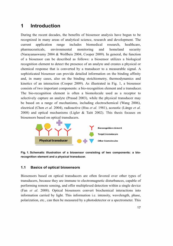
kinetics of an interaction (Cooper 2009). As illustrated in Fig. 1, a biosensor
consists of two important components: a bio-recognition element and a transducer.
The bio-recognition element is often a biomolecule used as a receptor to
selectively capture an analyte (Prasad 2003), while the physical transducer may
be based on a range of mechanisms, including electrochemical (Wang 2006),
electrical (Chen et al. 2004), radioactive (Hsu et al. 1981), acoustic (Länge et al.
2008) and optical mechanisms (Ligler & Taitt 2002). This thesis focuses on
biosensors based on optical transducers.
Physical transducer
Fig. 1. Schematic illustration of a biosensor consisting of two components: a bio-
recognition element and a physical transducer.
1.1 Basics of optical biosensors
Biosensors based on optical transducers are often favored over other types of
transducers, because they are immune to electromagnetic disturbances, capable of
performing remote sensing, and offer multiplexed detection within a single device
(Fan et al. 2008). Optical biosensors convert biochemical interactions into
information carried by light. This information i.e. intensity, wavelength, phase,
polarization, etc., can then be measured by a photodetector or a spectrometer. This
18
type of sensors is widely used in two detection protocols: fluorescent-based
detection and label-free detection. In a fluorescent-based detection scheme,
labeling of target molecules or receptors usually needs to be prepared in advance.
This process is both labor intensive and time-consuming, and the fluorescent
marker may interfere with the function of the labeled biomolecule (Ray et al.
2010). In a label-free detection scheme, on the other hand, the properties of light
are directly manipulated by biochemical interactions to produce a real-time signal
without affecting the targeted molecules. The most common method in label-free
detection involves monitoring effective refractive index (RI) changes resulting
from biomolecular interactions. Effective RI changes take place on a sensing
surface coated with immobilized receptors. By binding to the receptors, target
molecules change the thickness of the surface adlayer, thereby inducing a change
in the effective refractive index. Such changes are probed by an evanescent field
at the surface of an optic fiber or a waveguide. By using the evanescent field, a
sensitive determination of the refractive index changes on the near adjacent of the
waveguide surface can be obtained in integrated optical sensors.
1.2 Integrated evanescent field biosensors
Integrated optical (IO) sensors have drawn a great interest in the past a few
decades, because they allow sensitive, real-time, label-free, on-site measurements
of biochemical species (Lambeck 2006). Most IO sensors are based on a planar
multilayer waveguide structure, deposited on top of a silicon or glass substrate. A
multilayer waveguide structure consists of a very thin higher refractive index
layer, containing a network of optical waveguide channels, and adjacent lower
refractive index layers for light confinement. As a result of total internal reflection
(TIR) of light propagating in the layer with the higher refractive index, an
evanescent wave field penetrates the boundaries of the layer and reaches the top
of the waveguide surface with a typical penetration depth of a few hundred
nanometers, which is sufficient for the study of biochemical interactions (Ligler
& Taitt 2002). This type of planar waveguide geometry allows facile integration
with sample delivery and detection systems, as well as the functionalization and
patterning of recognition element arrays onto the surface, enabling the
simultaneous detection of multiple analytes using a single waveguide transducer
(Mukundan et al. 2009).
Ever since the introduction of the first IO biosensor based on grating couplers
(Lukosz & Tiefenthaler 1984), IO sensors of many different configurations have
19
been developed, including grating couplers (Vörös et al. 2002), interferometer
sensors (Prieto et al. 2003), resonant mirrors (George et al. 1995), surface plasma
resonance (SPR) sensors (Homola et al. 1999), ring resonators (Ksendzov & Lin
2005) and photonic crystal waveguide sensors (Skivesen et al. 2007). Typical IO
sensors are usually fabricated using inorganic dielectrics such as SOI (Densmore
et al. 2008), Si3N4 (Ymeti et al. 2002), III-V group composites (Cassidy 2007),
metal oxides e.g. Ta2O5 (Schmitt et al. 2007), with claddings of SiO2. Fabrication
of inorganic dielectric-based waveguides poses high facility requirements.
Constructing a slab waveguide with its multilayer structure involves such
processes as sputtering, ion exchange, epitaxial growth or chemical vapor
deposition (CVD), while ridge/rib waveguides require conventional
photolithography and reactive ion etching (RIE) to define the wave-guiding
channel (Hunsperger 2009). These fabrication processes are both capital-intensive
and time-consuming. Typical sensitivity of bulk RI sensing devices or biosensors
based on inorganic dielectric materials have a limit of detection (LOD) above 10-6
refractive index units (RIU), approaching 10-8 RIU for homogeneous refractive
index sensing. In surface sensing of molecule adsorption, a LOD of 13 fg/mm2 in
surface mass density has been achieved (Schmitt et al. 2007).
1.3 Motivation of the thesis
In recent years, polymers have become important materials for optical
waveguides, because of their good optical properties, versatile processability and
potential for low-cost production. Polymers can be easily processed with various
molding techniques at relatively low temperatures. As a result, they have become
suitable complementary materials to inorganic dielectrics in waveguide sensor
fabrication.
The key motivation for this work is to develop low-cost, high-performance,
disposable optical sensors based on polymeric materials for biosensing
applications in aqueous environments. To achieve that end, the following issues
were taken into consideration during the sensor development:
1. A fabrication process targeted on polymeric materials needs to be developed
based on molding technologies. The process should enable high-volume,
low-cost production of polymer IO biosensors.
2. To simplify the fabrication process and enhance usability, new sensor
structures and waveguide configurations need to be utilized and evaluated.

20
3. To achieve a performance level comparable to inorganic dielectric based
biosensors, the sensitivity of polymer-based sensors needs to be improved.
21
2 Waveguide biosensors in theory
In an optical waveguide, the higher refractive index of the core layer allows total
internal reflection of light at the core-cladding interface. A light beam coupled
into the waveguide is confined in the core and guided through to the end facet of
the waveguide. Light propagation in optical waveguides is usually described as an
electromagnetic wave having angular frequency ω propagating in the z direction
with propagation constant β. The electric field is expressed by:
( ) ( )ztjeyxEzyxE βω −= ,),,( , (1)
The propagation constant β is the z-directed component of the wave number k.
The ratio of the propagation constant β in a medium to the wave number k0 in
vacuum is called the effective refractive index neff:
0k
neff
β= . (2)
2.1 Theory behind waveguide biosensors utilizing evanescent field
probe
When light propagates in a dielectric waveguide, the boundary condition of the
electromagnetic field must be satisfied. That is, the tangential component of the
electric field E|| and magnetic field H|| should be continuous across the boundary.
In order to satisfy the boundary condition, a non-vanishing solution to Maxwell’s
equations is found, suggesting the existence of a non-travel wave at the boundary.
This means that, although light energy is totally reflected, an electromagnetic
field extends out from the interface into the lower index medium as shown in Fig.
2. This field is called evanescent field, and it decays exponentially with distance
from the surface, generally around a depth of 100 nm (Taitt et al. 2005).
22
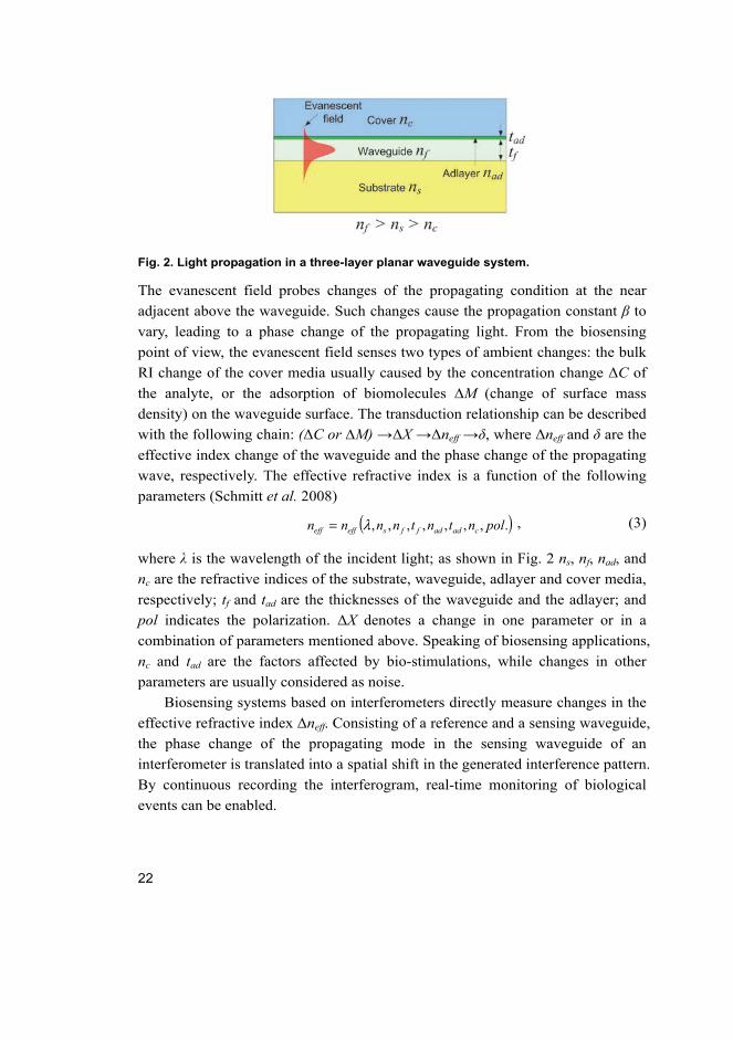
Fig. 2. Light propagation in a three-layer planar waveguide system.
The evanescent field probes changes of the propagating condition at the near
adjacent above the waveguide. Such changes cause the propagation constant β to
vary, leading to a phase change of the propagating light. From the biosensing
point of view, the evanescent field senses two types of ambient changes: the bulk
RI change of the cover media usually caused by the concentration change ΔC of
the analyte, or the adsorption of biomolecules ∆M (change of surface mass
density) on the waveguide surface. The transduction relationship can be described
with the following chain: (ΔC or ∆M) →ΔX →Δneff →δ, where Δneff and δ are the
effective index change of the waveguide and the phase change of the propagating
wave, respectively. The effective refractive index is a function of the following
parameters (Schmitt et al. 2008)
( ).,,,,,,, polntntnnnn cadadffseffeff λ= , (3)
where λ is the wavelength of the incident light; as shown in Fig. 2 ns, nf, nad, and
nc are the refractive indices of the substrate, waveguide, adlayer and cover media,
respectively; tf and tad are the thicknesses of the waveguide and the adlayer; and
pol indicates the polarization. ΔX denotes a change in one parameter or in a
combination of parameters mentioned above. Speaking of biosensing applications,
nc and tad are the factors affected by bio-stimulations, while changes in other
parameters are usually considered as noise.
Biosensing systems based on interferometers directly measure changes in the
effective refractive index Δneff. Consisting of a reference and a sensing waveguide,
the phase change of the propagating mode in the sensing waveguide of an
interferometer is translated into a spatial shift in the generated interference pattern.
By continuous recording the interferogram, real-time monitoring of biological
events can be enabled.
23
2.2 Young interferometer
Interferometer sensors typically consist of a reference arm and a sensing arm,
offering inherent background compensation for environmental disturbances, such
as temperature fluctuations. Interferometry is considered one of the most sensitive
techniques for optical sensing (Lukosz 1991). Different from the most commonly
used Mach-Zehnder interferometer, an IO Young interferometer (YI) generates a
complete periodic intensity pattern. It allows determining the absolute sign of the
induced phase change and produces a linear correlation between the spatial
change of the interference pattern and the induced phase change (Cross et al.
1999). For these reasons, the Young interferometer was chosen as the biosensor
development platform in this thesis.
2.2.1 Structures of Young interferometer
Three different structures of YI are commonly used in IO sensors, including a
horizontally-placed double-rib/strip waveguide structure (Schmitt et al. 2007, Qi
et al. 2009), a vertically-placed double-slab waveguide structure (Cross et al.
2003, Ricard-Blum et al. 2006) and a Y-junction structure (Brandenburg et al.
2000, Ymeti et al. 2005). This thesis utilized the latter two structures in polymer
biosensor developing. The dual-slab waveguide interferometer, shown in Fig. 3a,
was first developed in 1999 by Cross et al. (Cross et al. 1999). The vertical
structure contains alternatively stacked thin layers of waveguide claddings and
cores. Unlike traditional horizontally integrated Y-junction YIs, the slab-
waveguide YI does not need to be patterned for the structure of the Y-junction.
Moreover, the vertically-integrated structure offers the benefit of high tolerance to
misalignments of in-coupling light, since horizontal alignment is not required.
The Y-junction YI shown in Fig. 3b was also used, due to the existence of such
patterning methods, as imprinting and moulding, that are dedicated to polymers
and can be applied to simplify the fabrication process.
24
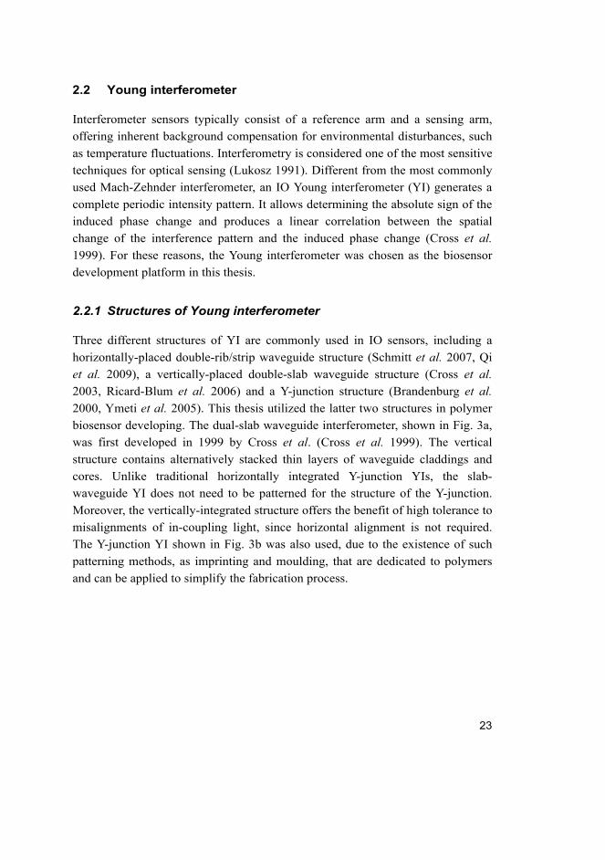
a) b)
Fig. 3. Structures of Young interferometer a) vertical spaced dual-slab Young
interferometer; b) Y-junction Young’s interferometer (Paper II & V, published by
permission of (c) 2012 OSA).
In both structures, a common input light beam launched at the input facet is split
and propagates through both waveguides simultaneously. The two separated
beams diffract out when they reach the output end-facet and interfere with each
other. Preferably an equal distribution of light in both waveguides is required in
order to optimize the visibility of the interferogram. In the far-field, a fringe
pattern is generated by the overlapping of the outgoing divergent beams. The
irradiance I of the interferogram pattern can be described by the following
equation (Hariharan 2003)
)cos(2 2121 δϕ −Δ++= IIIII , (4)
where I1 and I2 are the intensities of the two interfering beams, Δφ is the phase
difference between them, and δ is the additional phase shift caused by an effective
RI change in the sensing window. This change can be quantified by the following
expression
effnL Δ⋅=
0
2
λπδ , (5)
where L indicates interaction length (i.e., the length of the sensing window) and
λ0 is the vacuum wavelength of the monochromatic light source. When a stimulus,
i.e., a change in the analyte’s RI or attachment of biomolecules on the sensing
waveguide, appears, the effective RI of the propagating mode in the sensing
waveguide varies with respect to the wave propagating in the reference
waveguide. This produces a phase change of the generated interferogram,
displayed visually as a spatial shift of the fringe pattern.
25
2.3 Theoretical sensitivity analysis of polymer-based waveguide sensors
2.3.1 Determination of propagation constant by the Marcatili method
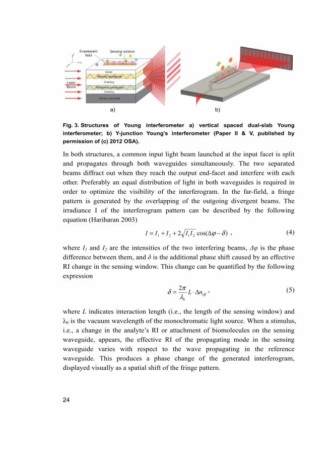
In slab and rib waveguides, the propagation constant β can be determined by the
Marcatili Method. It is an analytical method, designed to model two-dimensional
optical waveguides. Fig. 4 shows a cross-sectional view of a buried optical
waveguide. The core has a width of 2a and a height of 2b.
Fig. 4. Schematic illustration of the waveguide model used in the Marcatili method
(Paper I, published by permission of (c) 2008 SPIE).
In this method it is assumed that the electric and magnetic fields are confined to
the core and do not exist in the four hatched regions. By solving Maxwell’s
Equations, the following relations for wave numbers are obtained for the TE and
TM modes (Kawano & Kitoh 2001):
TE & TM:
22220 yxf kknk −−=β , (6)
TE:
( ) ( )12
arctan2222
0
2220
2220 −+
−−⋅
−−
= pk
knnk
knk
knkak
x
xcf
yc
yfx
π , (7)
( ) ( ) ( )12
arctan2
1arctan
2
12222
02222
0 −+
−−+
−−= q
k
knnk
k
knnkbk
y
ysf
y
ycf
y
π , (8)

26
TM:
( )( )
( ) ( )12
arctan2222
0
2220
2
2220
2
−+
−−⋅
−−
= pk
knnk
knkn
knknak
x
xcf
xcf
xfcx
π (9)
( ) ( ) ( )12
arctan2
1arctan
2
12222
0
2
222220
2
2
−+
−−+
−−= q
k
knnk
n
n
k
knnk
n
nbk
y
ysf
c
f
y
ycf
c
fy
π (10)
where k0 = 2π/λ0 is the wave number in vacuum and kx and ky are the wave
numbers in the x and y directions. As shown in Fig. 4, a and b are the half width
and length of the waveguide, while p and q are integers corresponding to the
numbers of the optical power peaks in the x and y directions. Unlike ordinary
mode orders, they start from 1 instead of 0.
With equation (2), the effective refractive index of the guided mode can be
derived from the propagation constant. This index is required in the next section
to analyze the theoretical sensitivity of the waveguide sensor.
2.3.2 The sensitivities to the change of bulk RI and adlayer thickness
IO waveguide biosensors respond to changes in the bulk RI of the cover media
and to the surface adsorption of biomolecues. A stimulated change on the
effective RI can be described by
ad
ad
effc
c
effeff t
t
nn
n
nn Δ
∂∂
+Δ∂∂
=Δ , (11)
where the derivatives ∂neff/∂nc and ∂neff/∂tad are the sensitivity of the waveguide to
the bulk RI change ∆nc and the thickness change of the biomolecule adlayer ∆tad
correspondingly. When the wavelength of the propagating wave and the physical
parameters of the waveguide structure are known, the sensitivities ∂neff/∂nc and
∂neff/∂tad can be defined by the following equations according to (Tiefenthaler &
Lukosz 1989)
ρ
−
Δ=
∂∂
12
2
,
c
eff
eff
cf
eff
c
c
eff
n
n
t
z
n
n
n
n , (12)
( ) ( )( ) ( )
ρ
−+
−+−−−
=∂∂
1
122
22
22
2222
feffceff
adeffceff
cf
cad
effeff
efff
ad
eff
nnnn
nnnn
nn
nn
tn
nn
t
n , (13)
27
where ρ = 0 for TE modes and ρ = 1 for TM modes. nad is the refractive index of
the adlayer and teff is the effective waveguide thickness given by
=
Δ+=csj
jffeff ztt,
,, (14)
tf is the waveguide thickness and ∆zf,j is the penetration depth of the evanescent
field into the substrate (j = s) or cover medium (j = c).
( ) ( )[ ]22
0
122
220
,
11
jeff
jefffeff
jeff
jfnnk
nnnn
nnkz
−
−++
−
−=Δ−
ρρ , (15)
where ρ equals 0 for the TE mode and 1 for the TM mode. Using Ormocore for
the waveguide core, Ormocomp for the substrate and water for the cover medium,
the sensitivity of the waveguide can be studied with respect to the different
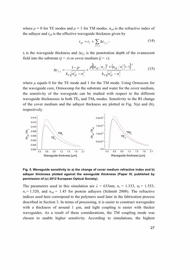
waveguide thicknesses in both TE0 and TM0 modes. Sensitivity to the RI change
of the cover medium and the adlayer thickness are plotted in Fig. 5(a) and (b),
respectively.
0.3 0.6 0.9 1.2 1.5 1.8 2.10.000
0.002
0.004
0.006
0.008
0.010
0.012
0.014
∂nef
f /∂n
c
Waveguide thickness [μm]
TE0
TM0
0.3 0.6 0.9 1.2 1.5 1.8 2.10.0
5.0x10⁻⁶
1.0x10⁻⁵
1.5x10⁻⁵
2.0x10⁻⁵
TE0∂n
eff
/∂t ad
Waveguide thickness [μm]
TM0
Fig. 5. Waveguide sensitivity to a) the change of cover medium refractive index and b)
adlayer thickness plotted against the waveguide thickness (Paper IV, published by
permission of (c) 2012 European Optical Society).
The parameters used in this simulation are λ = 633nm, nc = 1.333, nf = 1.553,
ns = 1.520, and nad = 1.45 for protein adlayers (Schmitt 2008). The refractive
indices used here correspond to the polymers used later in the fabrication process
described in Section 3. In terms of processing, it is easier to construct waveguides
with a thickness of around 1 µm, and light coupling is easier with thicker
waveguides. As a result of these considerations, the TM coupling mode was
chosen to enable higher sensitivity. According to simulations, the highest
28
sensitivities are achieved at a waveguide thickness of 580 nm with maximum
values of ∂neff/∂nc = 0.0134 and ∂neff/∂tad = 2.1×10⁻⁵ nm-1.
With longer radiation wavelength, the penetration depth would become longer.
However, in usual biosensing applications with the size of biomolecules up to a
few nanomemters, a much longer penetration depth is not necessary. Besides, in
the application point of view, visible wavelength is much easier to handle in cases
like light coupling and detection. Therefore the visible wavelength was selected
for measurements in this thesis. The near infra-red wavelength was only used for
testing purposes.
29
3 Sensor design, fabrication and characterization
This section provides a detailed description of the material, structure, fabrication
process and device characterization of the developed sensors. Owing to the
unique benefits possessed by the different Young interferometer structures, both
the vertically-spaced dual-slab and the conventional Y-junction based structure
described in Subsection 2.2.1 were utilized in the fabrication of the polymer-
based interferometric sensors.
3.1 Polymers in integrated optics
Research on the use of organic materials for integrated optics started in the early
1970s (Tien 1971). As polymers represent a new material available for optical
integrated optics, they are less studied than semiconductors and inorganic
dielectrics within the telecommunications industry (Paloczi 2005). In recent years,
the driving force of the market has greatly increased the demand for large
quantities of inexpensive IO devices, and polymeric materials certainly satisfy
this requirement.
Polymers possess many good features, including high optical transmittance,
low dispersion and a refractive index that is tunable within a limited range. Most
importantly, polymers offer versatile processability. Thus, in contrast to
semiconductor materials that require several successive thin-film growths and
photolithography with expensive equipment, optical polymers lend themselves to
flexible, large area, low-cost fabrication of waveguide devices through simple
spin-coating techniques and low-temperature processing. Moreover, they are fully
compatible with semiconductor electronics. By controlling the ratio of the
polymer diluted in the solvent and spinning speed, a coated film can achieve a
thickness in the range of 0.1 to 100 µm (Ma et al. 2002). Due to easy
processability, a variety of substrates are compatible for polymer waveguide
devices, such as glass, silicon dioxide, silicon, indium phosphide—and even
certain types of polymers (Chang-Yen et al. 2005).
The fabrication process of polymer waveguides will be summarized here
briefly. For slab waveguides, where the optical field is vertically confined, spin
coating or dip coating are usually applied to the deposition of multilayer thin
films on the chosen substrate. For rib waveguides, confinement of the optical field
in the lateral direction requires patterning of the polymer. Various techniques
30
available for patterning fall into the following categories: photoresist-based
photolithography (Usui et al. 1996), direct photolithography (Cha et al. 2004),
soft lithography (Unger et al. 2000) and moulding (Heckele & Schomburg 2004).
Photoresist-based photolithography, which utilizes masks, is directly adopted
from standard semiconductor processing technology, where photolithography is
performed on the photoresist layer coated on the polymer and the developed
pattern is transferred into the polymer by RIE. For photosensitive polymers,
direct photolithography can be used to pattern waveguides by conventional mask
photolithography or direct laser writing (Eldada et al. 1996). Photosensitive
polymers behave like negative tone photoresists, and polymerization is caused by
exposure to ultraviolet (UV) light. Being confined to the polymer fabrication
process, non-photolithographic techniques, i.e., soft lithography and moulding,
are not available for more conventional photonic materials, such as glass and
semiconductors (Eldada et al. 2000). These unique techniques for polymer
processing are simple to perform and require less complicated, low-cost
equipment. There is no clear distinction between these two techniques, since they
both use a mould to transfer patterns. However, soft lithography utilizes
polydimethylsiloxane (PDMS) moulds to transfer micropatterns. The moulds
themselves are made of hard materials, such as aluminium, nickel, silicon or even
hardened polymers (Wang et al. 2011), which allow quick prototyping. Often
used moulding techniques for thermal plastics are injection moulding and hot
embossing, while the UV nanoimprint lithography (NIL) technique is utilized for
photosensitive polymers.
UV-NIL is usually performed at low pressure and room temperature. By
pressing a transparent mould with nano-/microscale features on a UV-sensitive
thin resin layer or droplet and curing it under UV light, a replica of the mould is
formed. NIL relies on direct mechanical deformation of the resist material and can
therefore achieve resolutions beyond the limitations set by light diffraction or
beam scattering that are encountered in conventional photolithography (Guo
2007). This technique is capable of producing high-resolution nanoscale features
down to sub-10 nm with high throughput (Kuo et al. 2003).
3.1.1 Polymeric IO biosensors
Besides the easy processability mentioned above, another advantage of polymer-
based IO devices is their high potential for use as chemical and biological sensors,
31
because the organic groups in a polymeric compound can be designed and
tailored to react against a specific medium (Lifante 2003).
Several polymer-based planar waveguide sensors have been developed
recently, such as ring resonators (Chao et al. 2006, Kim et al. 2008), polarometric
interferometers (Kwon et al. 2009), Mach-Zehnder interferometers (Shew et al.
2008, Bruck et al. 2011) and grating couplers (Oh et al. 2006, Kim et al. 2010).
The sensitivity of these previously reported polymer biosensors for bulk refractive
index changes is in the order of sub-10-5 RIU. As the RI of polymer materials
ranges from 1.3 to 1.7, there is very little variation between different materials,
leading to a low RI contrast (typically < 0.3) between the core and the cladding in
a polymer waveguide. For the commonly used cladding material SiO2 (n = 1.46),
the highest sensitivity achievable in a three-layer waveguide system can be
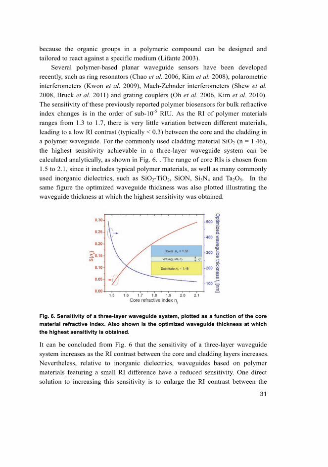
calculated analytically, as shown in Fig. 6. . The range of core RIs is chosen from
1.5 to 2.1, since it includes typical polymer materials, as well as many commonly
used inorganic dielectrics, such as SiO2-TiO2, SiON, Si3N4 and Ta2O5. In the
same figure the optimized waveguide thickness was also plotted illustrating the
waveguide thickness at which the highest sensitivity was obtained.
Fig. 6. Sensitivity of a three-layer waveguide system, plotted as a function of the core
material refractive index. Also shown is the optimized waveguide thickness at which
the highest sensitivity is obtained.
It can be concluded from Fig. 6 that the sensitivity of a three-layer waveguide
system increases as the RI contrast between the core and cladding layers increases.
Nevertheless, relative to inorganic dielectrics, waveguides based on polymer
materials featuring a small RI difference have a reduced sensitivity. One direct
solution to increasing this sensitivity is to enlarge the RI contrast between the
32
cladding and the core. To that end, Horváth et al. utilized a nanoporous silica
substrate with a refractive index of 1.2, while other research groups exploited the
fluorinated polymer Cytop with a RI of 1.34 (Agnarsson et al. 2010, Kim et al.
2010) as cladding material. Another way to increase sensitivity is to deposit a
high RI coating above the polymer waveguide, such as TiO2 deposited on a
polymer waveguide (Kwon et al. 2009) and a Ta2O5 coating on a glass waveguide
(Qi et al. 2009).
3.1.2 Ormocer - organic and inorganic hybrid polymer
ORMOCER® is a series of inorganic-organic hybrid polymers commercialized by
micro resist technology GmbH in Germany. A combination of good optical and
dielectric properties makes it a good candidate for electro-optical applications
(Buestrich et al. 2001). It is highly transparent above the wavelength of 400 nm
and up to the near-infrared region. At 633 nm, optical loss of the series of
materials is less than 0.1 dB/cm.
The Ormocer series contains several different polymeric materials. Three of
them, Ormocore, Ormoclad and Ormocomp, were used in this work. Their
refractive indices are 1.553, 1.536 and 1.520, respectively, determined at the
wavelength of 633 nm with a Metricon prism coupler. Taking into consideration
the fabrication process, optical waveguides can be produced within one material
class, and the processing is compatible to conventional equipment used in thin-
film processing of wafer-scale devices. Moreover, Ormocer materials are easy to
handle and offer good adhesion on most substrates, such as Si wafers, inorganic
glasses and polymers. Most importantly, Ormocers are photosensitive, allowing
curing under UV exposure. The ability to be patterned by UV irradiation makes
them attractive for any kind of wafer-scale application (Houbertz et al. 2003).
Although they behave like negative photoresists, their thermal and chemical
stability is better, due to a backbone composed of inorganic Si-O-Si networks
(Streppel et al. 2003). This unique feature results in a decomposition temperature
of ≈ 270 °C, which is sufficiently high for most technical applications.
3.2 Dual-slab Young interferometers
One of the sensing structures investigated in this thesis is the dual-slab waveguide
structure. As shown in the schematic illustration in Fig. 3a, it is a five-layer
structure with alternatively stacked cores and claddings. When a light beam with
33
a diameter larger than the inter-cladding between both cores shines on the facet of
the multilayer stack, the beam split up and propagates in both cores. At the other
end of the stack, the two beams diffract out and interfere with each other,
generating a fringe pattern. The principle behind this phenomenon fits perfectly to
that of a YI. Unlike traditional horizontally-integrated Y-junction YIs, the dual-
slab Young interferometer is vertically spaced and does not need Y-junction
patterning for light splitting. Moreover, its vertically-integrated structure offers
the benefit of high tolerance to misalignment of the in-coupling light. Due to the
multi-layer structure of the slab waveguide interferometer, it is easy to fabricate
the sensor using polymer materials. Each layer can be deposited by spin-coating
and the thickness is adjustable by varying the coating speed.
3.2.1 Fabrication process and waveguide characterization
In the fabrication of the dual-slab Young interferometer-based polymer sensors
described here, Ormocomp was used as cladding layer and Ormocore as core
layer material. Single-crystal silicon 4” wafers were selected as substrates, owing
to their smooth end-facets after cleaving. Apart from mere mechanical support,
the substrate does not offer any additional functionality. Above the Si substrate, a
thick layer (>10 µm) of Ormocomp was deposited with the imprinting method by
pressing a blank glass wafer against the dispensed resin. After curing under
broadband UV exposure, the wafer was placed in a plasma etcher (Pico, Diener
Electronic GmbH) for 30 s to open the bonds on the imprinted Ormocomp layer.
Subsequent layers were deposited one after another by the spin-coating technique
with a common speed of 3000 rpm for 60 seconds. After the curing of each coated
layer, plasma etching was performed for 30 s, before coating of the next layer. Fig.
7a shows a cross-section image of the finished structure under SEM (JCM-5000
Neoscope, Jeol Ltd.). The thickness of the two waveguiding layers is ~1 µm and
that of the cladding layer between the two waveguides > 6 µm.
34
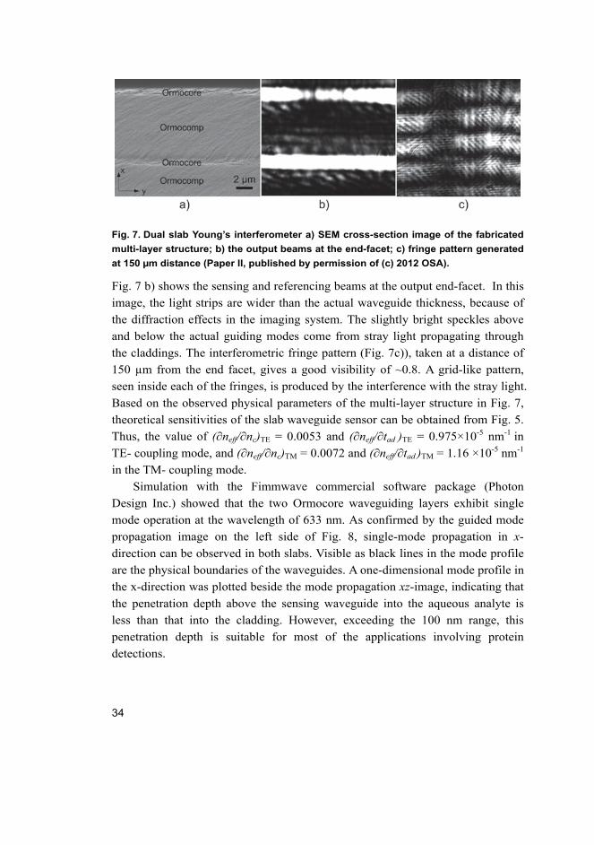
Fig. 7. Dual slab Young’s interferometer a) SEM cross-section image of the fabricated
multi-layer structure; b) the output beams at the end-facet; c) fringe pattern generated
at 150 µm distance (Paper II, published by permission of (c) 2012 OSA).
Fig. 7 b) shows the sensing and referencing beams at the output end-facet. In this
image, the light strips are wider than the actual waveguide thickness, because of
the diffraction effects in the imaging system. The slightly bright speckles above
and below the actual guiding modes come from stray light propagating through
the claddings. The interferometric fringe pattern (Fig. 7c)), taken at a distance of
150 µm from the end facet, gives a good visibility of ~0.8. A grid-like pattern,
seen inside each of the fringes, is produced by the interference with the stray light.
Based on the observed physical parameters of the multi-layer structure in Fig. 7,
theoretical sensitivities of the slab waveguide sensor can be obtained from Fig. 5.
Thus, the value of (∂neff/∂nc)TE = 0.0053 and (∂neff/∂tad )TE = 0.975×10⁻⁵ nm-1 in
TE- coupling mode, and (∂neff/∂nc)TM = 0.0072 and (∂neff/∂tad )TM = 1.16 ×10⁻⁵ nm-1
in the TM- coupling mode.
Simulation with the Fimmwave commercial software package (Photon
Design Inc.) showed that the two Ormocore waveguiding layers exhibit single
mode operation at the wavelength of 633 nm. As confirmed by the guided mode
propagation image on the left side of Fig. 8, single-mode propagation in x-
direction can be observed in both slabs. Visible as black lines in the mode profile
are the physical boundaries of the waveguides. A one-dimensional mode profile in
the x-direction was plotted beside the mode propagation xz-image, indicating that
the penetration depth above the sensing waveguide into the aqueous analyte is
less than that into the cladding. However, exceeding the 100 nm range, this
penetration depth is suitable for most of the applications involving protein
detections.
35
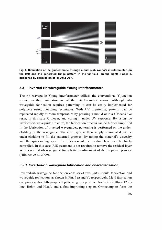
Fig. 8. Simulation of the guided mode through a dual slab Young’s interferometer (on
the left) and the generated fringe pattern in the far field (on the right) (Paper II,
published by permission of (c) 2012 OSA).
3.3 Inverted-rib waveguide Young interferometers
The rib waveguide Young interferometer utilizes the conventional Y-junction
splitter as the basic structure of the interferometric sensor. Although rib-
waveguide fabrication requires patterning, it can be easily implemented for
polymers using moulding techniques. With UV imprinting, patterns can be
replicated rapidly at room temperature by pressing a mould onto a UV-sensitive
resin, in this case Ormocer, and curing it under UV exposure. By using the
inverted-rib waveguide structure, the fabrication process can be further simplified.
In the fabrication of inverted waveguides, patterning is performed on the under-
cladding of the waveguide. The core layer is then simply spin-coated on the
under-cladding to fill the patterned grooves. By tuning the material’s viscosity
and the spin-coating speed, the thickness of the residual layer can be finely
controlled. In this case, RIE treatment is not required to remove the residual layer
as in a normal rib waveguide for a better confinement of the propagating mode
(Hiltunen et al. 2009).
3.3.1 Inverted-rib waveguide fabrication and characterization
Inverted-rib waveguide fabrication consists of two parts: mould fabrication and
waveguide replication, as shown in Fig. 9 a) and b), respectively. Meld fabrication
comprises a photolithographical patterning of a positive photoresist (Ultra-i 123 I-
line, Rohm and Haas), and a first imprinting step on Ormocomp to form the
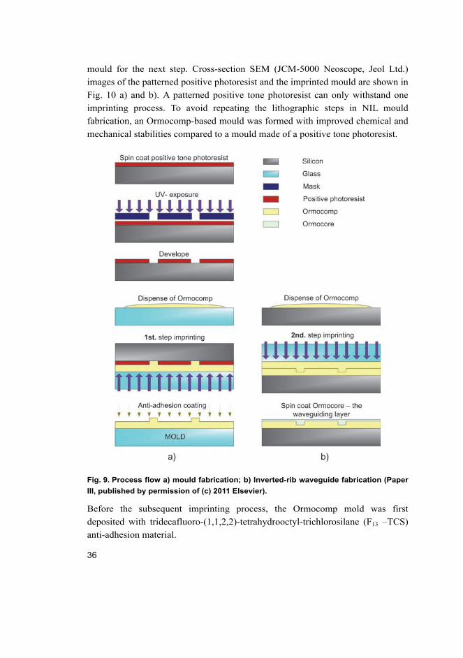
36
mould for the next step. Cross-section SEM (JCM-5000 Neoscope, Jeol Ltd.)
images of the patterned positive photoresist and the imprinted mould are shown in
Fig. 10 a) and b). A patterned positive tone photoresist can only withstand one
imprinting process. To avoid repeating the lithographic steps in NIL mould
fabrication, an Ormocomp-based mould was formed with improved chemical and
mechanical stabilities compared to a mould made of a positive tone photoresist.
Fig. 9. Process flow a) mould fabrication; b) Inverted-rib waveguide fabrication (Paper
III, published by permission of (c) 2011 Elsevier).
Before the subsequent imprinting process, the Ormocomp mold was first
deposited with tridecafluoro-(1,1,2,2)-tetrahydrooctyl-trichlorosilane (F13 –TCS)
anti-adhesion material.
37
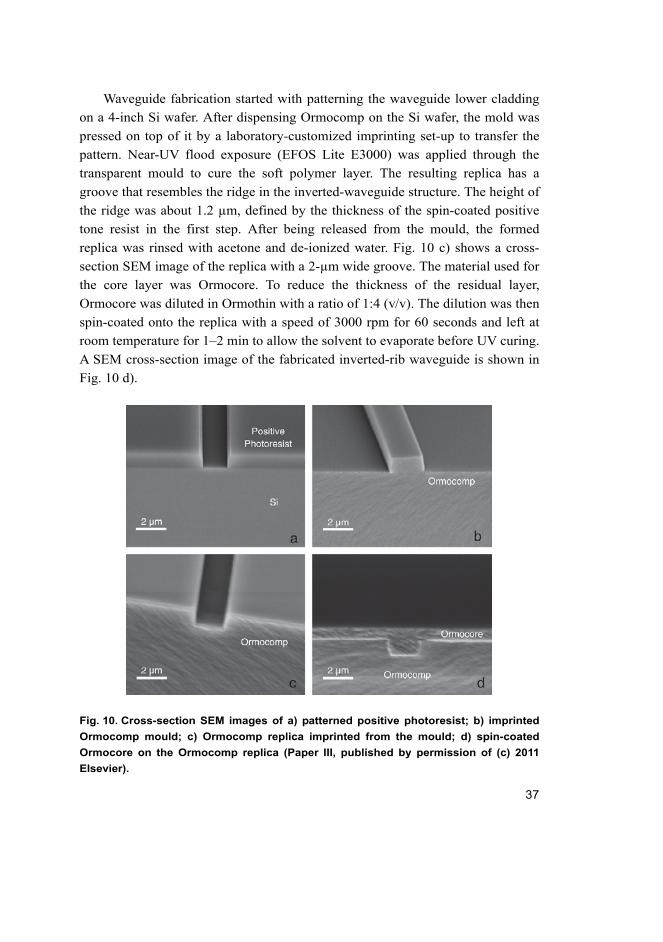
Waveguide fabrication started with patterning the waveguide lower cladding
on a 4-inch Si wafer. After dispensing Ormocomp on the Si wafer, the mold was
pressed on top of it by a laboratory-customized imprinting set-up to transfer the
pattern. Near-UV flood exposure (EFOS Lite E3000) was applied through the
transparent mould to cure the soft polymer layer. The resulting replica has a
groove that resembles the ridge in the inverted-waveguide structure. The height of
the ridge was about 1.2 µm, defined by the thickness of the spin-coated positive
tone resist in the first step. After being released from the mould, the formed
replica was rinsed with acetone and de-ionized water. Fig. 10 c) shows a cross-
section SEM image of the replica with a 2-µm wide groove. The material used for
the core layer was Ormocore. To reduce the thickness of the residual layer,
Ormocore was diluted in Ormothin with a ratio of 1:4 (v/v). The dilution was then
spin-coated onto the replica with a speed of 3000 rpm for 60 seconds and left at
room temperature for 1–2 min to allow the solvent to evaporate before UV curing.
A SEM cross-section image of the fabricated inverted-rib waveguide is shown in
Fig. 10 d).
Fig. 10. Cross-section SEM images of a) patterned positive photoresist; b) imprinted
Ormocomp mould; c) Ormocomp replica imprinted from the mould; d) spin-coated
Ormocore on the Ormocomp replica (Paper III, published by permission of (c) 2011
Elsevier).
38
The root-mean-square (RMS) surface roughness of the replica (Fig. 10 c)) and of
the inverted-waveguide structure (Fig. 10 d)) were examined using atomic force
microscopy (AFM, Veeco Dimensions 3100). An average of 6 measurements
showed that the RMS surface roughness of the replica (Ormocomp lower
cladding layer) was 0.54 ± 0.09 nm, while that of the inverted-rib waveguide was
1.61 ± 0.19 nm. Thus, the RMS surface roughness of the replica was in fairly
good agreement with the with RMS values for positive-tone photoresist (Fig. 10
a)) and the mould (Fig. 10 b)), 0.48 ± 0.02 nm and 0.8 ± 0.2 nm, respectively,
reported by Jussi et al. This demonstrates that a fabrication process with two
consecutive imprinting procedures is capable of producing a very smooth surface
on the moulded lower cladding layer in the inverted-waveguide structure. Also
thickness variations of the spin-coated core layer were inspected under SEM. In
the 4 cm range, the core layer’s thickness was about 0.9 µm ± 0.1 µm, confirming
that the spin-coated core layer is fairly uniform. Based on visual inspection, the
core layer uniformly covered the entire 4" substrate.
A detailed characterization of the fabricated inverted-rib waveguide was
presented in Paper III. With an excitation light source of 1310 nm, the waveguide
operated in single mode, achieving a transmittance of close to 60% in a 3 cm long
waveguide. This result is promising even for IO interconnection applications in
the telecommunications industry. Although scattering is expected to be higher at
632.8 nm, the wavelength used in the experiments reported in this thesis, than in
the infrared range, the transmitted light power is still sufficient for biosensing
applications.
3.3.2 Rib-waveguide for Young interferometers
The upper-cladding of the rib-waveguide Young interferometer was formed by
spin-coating a thick ~ 20 µm layer of Ormoclad above the core. A sensing
window was then opened above the waveguide using photolithography. Finally,
the fabricated waveguide sensor was hard-baked for 2 hours in an oven at 150°. A
schematic design of the Young interferometer sensor based on a Y-junction rib-
waveguide is shown in Fig. 11, with corresponding microscope images. These
microscope illustrations omit the middle section of the interferometer due to the
relatively long structure of the waveguide.
39
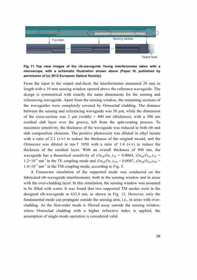
Fig. 11. Top view images of the rib-waveguide Young interferometer taken with a
microscope, with a schematic illustration shown above (Paper IV, published by
permission of (c) 2012 European Optical Society).
From the input to the output end-facet, the interferometer measured 20 mm in
length with a 10 mm sensing window opened above the reference waveguide. The
design is symmetrical with exactly the same dimensions for the sensing and
referencing waveguide. Apart from the sensing window, the remaining sections of
the waveguides were completely covered by Ormoclad cladding. The distance
between the sensing and referencing waveguide was 50 µm, while the dimension
of the cross-section was 2 µm (width) × 400 nm (thickness), with a 500 nm
residual slab layer over the groove, left from the spin-coating process. To
maximize sensitivity, the thickness of the waveguide was reduced in both rib and
slab composition elements. The positive photoresist was diluted in ethyl lactate
with a ratio of 2:1 (v/v) to reduce the thickness of the original mould, and the
Ormocore was diluted in ma-T 1050 with a ratio of 1:4 (v/v) to reduce the
thickness of the residual layer. With an overall thickness of 900 nm, the
waveguide has a theoretical sensitivity of (∂neff/∂nc )TE = 0.0064, (∂neff/∂tad )TE =
1.2×10⁻⁵ nm-1 in the TE coupling mode and (∂neff/∂nc )TM = 0.0087, (∂neff/∂tad )TM =
1.4×10⁻⁵ nm-1 in the TM coupling mode, according to Fig. 5.
A Fimmware simulation of the supported mode was conducted on the
fabricated rib-waveguide interferometer, both in the sensing window and in areas
with the over-cladding layer. In this simulation, the sensing window was assumed
to be filled with water. It was found that two supported TM modes exist in the
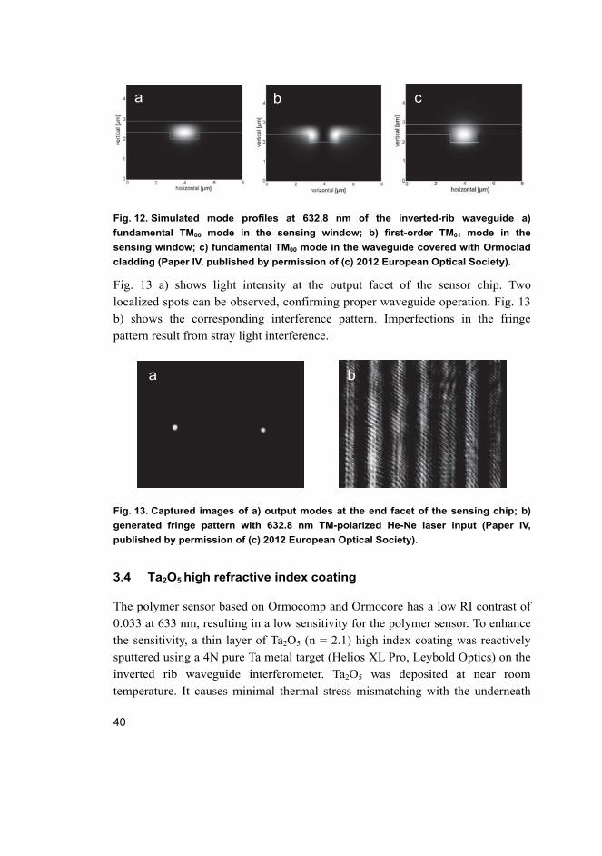
designed rib-waveguide at 632.8 nm, as shown in Fig. 12. However, only the
fundamental mode can propagate outside the sensing area, i.e., in areas with over-
cladding. As the first-order mode is filtered away outside the sensing window,
where Ormoclad cladding with a higher refractive index is applied, the
assumption of single-mode operation is considered valid.
40
Fig. 12. Simulated mode profiles at 632.8 nm of the inverted-rib waveguide a)
fundamental TM00 mode in the sensing window; b) first-order TM01 mode in the
sensing window; c) fundamental TM00 mode in the waveguide covered with Ormoclad
cladding (Paper IV, published by permission of (c) 2012 European Optical Society).
Fig. 13 a) shows light intensity at the output facet of the sensor chip. Two
localized spots can be observed, confirming proper waveguide operation. Fig. 13
b) shows the corresponding interference pattern. Imperfections in the fringe
pattern result from stray light interference.
Fig. 13. Captured images of a) output modes at the end facet of the sensing chip; b)
generated fringe pattern with 632.8 nm TM-polarized He-Ne laser input (Paper IV,
published by permission of (c) 2012 European Optical Society).
3.4 Ta2O5 high refractive index coating
The polymer sensor based on Ormocomp and Ormocore has a low RI contrast of
0.033 at 633 nm, resulting in a low sensitivity for the polymer sensor. To enhance
the sensitivity, a thin layer of Ta2O5 (n = 2.1) high index coating was reactively
sputtered using a 4N pure Ta metal target (Helios XL Pro, Leybold Optics) on the
inverted rib waveguide interferometer. Ta2O5 was deposited at near room
temperature. It causes minimal thermal stress mismatching with the underneath
a b c
a b
41
polymer layer, thus very good film quality can be achieved with no cracks. Ta2O5
has very low optical loss at both visible and infra-red wavelengths making it ideal
for planar waveguide applications (Pearce et al. 2012).
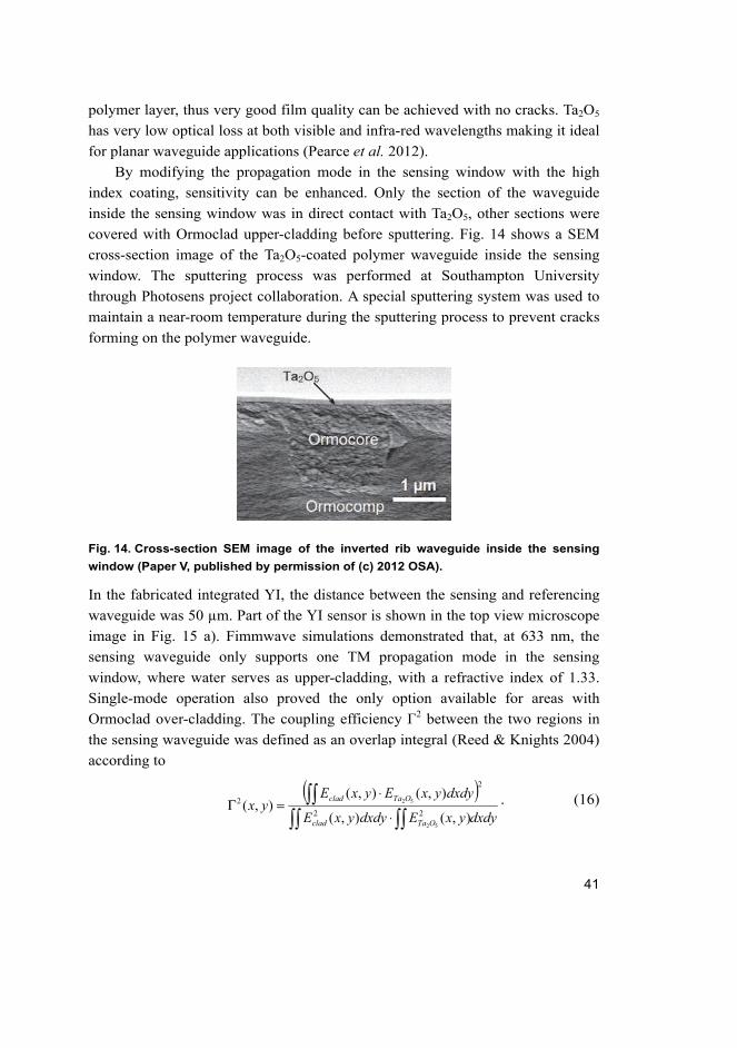
By modifying the propagation mode in the sensing window with the high
index coating, sensitivity can be enhanced. Only the section of the waveguide
inside the sensing window was in direct contact with Ta2O5, other sections were
covered with Ormoclad upper-cladding before sputtering. Fig. 14 shows a SEM
cross-section image of the Ta2O5-coated polymer waveguide inside the sensing
window. The sputtering process was performed at Southampton University
through Photosens project collaboration. A special sputtering system was used to
maintain a near-room temperature during the sputtering process to prevent cracks
forming on the polymer waveguide.
Fig. 14. Cross-section SEM image of the inverted rib waveguide inside the sensing
window (Paper V, published by permission of (c) 2012 OSA).
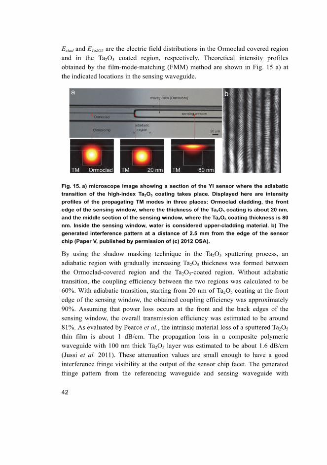
In the fabricated integrated YI, the distance between the sensing and referencing
waveguide was 50 µm. Part of the YI sensor is shown in the top view microscope
image in Fig. 15 a). Fimmwave simulations demonstrated that, at 633 nm, the
sensing waveguide only supports one TM propagation mode in the sensing
window, where water serves as upper-cladding, with a refractive index of 1.33.
Single-mode operation also proved the only option available for areas with
Ormoclad over-cladding. The coupling efficiency Γ2 between the two regions in
the sensing waveguide was defined as an overlap integral (Reed & Knights 2004)
according to
( )
⋅
⋅=Γ
dxdyyxEdxdyyxE
dxdyyxEyxEyx
OTaclad
OTaclad
),(),(
),(),(),(
22
2
2
52
52 . (16)
42
Eclad and ETa2O5 are the electric field distributions in the Ormoclad covered region
and in the Ta2O5 coated region, respectively. Theoretical intensity profiles
obtained by the film-mode-matching (FMM) method are shown in Fig. 15 a) at
the indicated locations in the sensing waveguide.
Fig. 15. a) microscope image showing a section of the YI sensor where the adiabatic
transition of the high-index Ta2O5 coating takes place. Displayed here are intensity
profiles of the propagating TM modes in three places: Ormoclad cladding, the front
edge of the sensing window, where the thickness of the Ta2O5 coating is about 20 nm,
and the middle section of the sensing window, where the Ta2O5 coating thickness is 80
nm. Inside the sensing window, water is considered upper-cladding material. b) The
generated interference pattern at a distance of 2.5 mm from the edge of the sensor
chip (Paper V, published by permission of (c) 2012 OSA).
By using the shadow masking technique in the Ta2O5 sputtering process, an
adiabatic region with gradually increasing Ta2O5 thickness was formed between
the Ormoclad-covered region and the Ta2O5-coated region. Without adiabatic
transition, the coupling efficiency between the two regions was calculated to be
60%. With adiabatic transition, starting from 20 nm of Ta2O5 coating at the front
edge of the sensing window, the obtained coupling efficiency was approximately
90%. Assuming that power loss occurs at the front and the back edges of the
sensing window, the overall transmission efficiency was estimated to be around
81%. As evaluated by Pearce et al., the intrinsic material loss of a sputtered Ta2O5
thin film is about 1 dB/cm. The propagation loss in a composite polymeric
waveguide with 100 nm thick Ta2O5 layer was estimated to be about 1.6 dB/cm
(Jussi et al. 2011). These attenuation values are small enough to have a good
interference fringe visibility at the output of the sensor chip facet. The generated
fringe pattern from the referencing waveguide and sensing waveguide with
43
adiabatic transitions is shown in Fig. 15 b). The clear visibility of the
interferogram gives a good resolution for analyzing fringe pattern phase shifts by
a two-dimensional (2D) fast Fourier transform (FFT). Like the fringe patterns
generated by the other two sensor structures: the polymer dual-slab and the
polymer inverted rib waveguide sensor structures, the grid-like patterns contained
in the fringe pattern was caused by the inference with the stray like. By using the
2D-FFT analyzing method, the high frequency noise does not degrade the
determination of the phase.
IO waveguide biosensors respond to changes in the bulk refractive index of
liquid samples and the surface adsorption of biomolecules. The bulk RI change of
a liquid sample is seen as a change in the refractive index of the upper-cladding nc.
The adsorption of biomolecules translates into a thickness change of the adlayer
tad, growing above the sensing waveguide. According to Equation (11), the
induced effective RI change Δneff of the sensing waveguide is a function of the
bulk refractive index change Δnc and the growth of the adlayer thickness Δtad.
Using the observed physical parameters of the inverted-rib waveguide structure
shown in Fig. 14, theoretical sensitivities of ∂neff/∂nc and ∂neff/∂tad were examined
using Fimmwave. To calculate ∂neff/∂tad, nad = 1.45 was used for the RI of the
adsorbed biomolecule layer. With increasing coating thickness, the optical field
distribution of the propagating mode is pushed up towards the waveguide surface,
resulting in increased power in the evanescent field, thus improved sensitivity. As
can be seen from Fig. 16 a) and b), the curves for homogeneous refractive-index
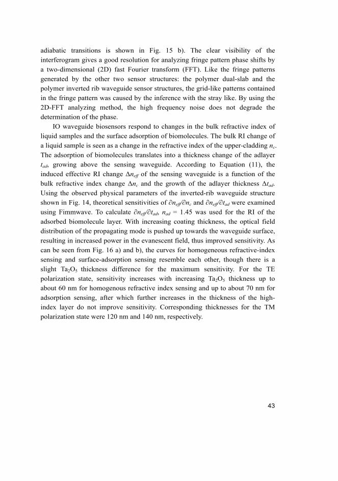
sensing and surface-adsorption sensing resemble each other, though there is a
slight Ta2O5 thickness difference for the maximum sensitivity. For the TE
polarization state, sensitivity increases with increasing Ta2O5 thickness up to
about 60 nm for homogenous refractive index sensing and up to about 70 nm for
adsorption sensing, after which further increases in the thickness of the high-
index layer do not improve sensitivity. Corresponding thicknesses for the TM
polarization state were 120 nm and 140 nm, respectively.
44
TE TM
0 20 40 60 80 100 120 140 160
0.00
0.04
0.08
0.12
0.16
0.20
0.24
∂nef
f/∂n c
Ta2O
5 thickness [nm]
a
0 20 40 60 80 100 120 140 160
0.0000
0.0001
0.0002
0.0003
0.0004
0.0005
∂nef
f/∂t ad
[nm
-1]
Ta2O
5 Thickness [nm]
TE TM
b
Fig. 16. Sensitivity of a) homogeneous refractive index sensing and b) surface sensing
of biomolecular adsorption as a function of the thickness of the Ta2O5 coating for both
TE- and TM- coupling modes (Paper V, published by permission of (c) 2012 OSA).
The observed enhancement in sensitivity is associated with decreased
confinement inside the inverted guiding ridge. When a much thicker high-index
coating is deposited on the polymer layers, the composite waveguide structure
becomes leaky. To optimize sensitivity and mode confinement in the sensing
region, 80 nm coating and TM polarization were chosen. According to
simulations, the obtained sensitivity of 80 nm Ta2O5 coating is 0.12 and 2.1×10⁻⁴
nm-1 for homogeneous RI and surface molecular adsorption sensing, respectively.
This sensitivity exceeded that of a polymer waveguide sensor without high-index
coating by over 40 times, while still retaining 17% power confinement inside the
inverted ridge, ensuring in proper waveguide operation.
45
4 Biosensor experiments and results
This thesis developed three polymer Young interferometer sensors based on
different waveguide configurations: dual-slab waveguide Young interferometer,
inverted-rib Young interferometer and inverted-rib Young interferometer with
Ta2O5 coating. For clarity, Fig. 17 shows schematic cross-section images of these
different structures. Several sensors were produced with each different structure,
only the best three samples were regarded in this thesis.
Fig. 17. The schematic cross-section images of the waveguide used to build a) dual-
slab waveguide Young interferometer sensor; b) polymer inverted rib waveguide
Young interferometer sensor; c) polymeric-inorganic composite waveguide Young
interferometer sensor with inverted rib waveguide structure.
Sensor performance was evaluated in terms of homogeneous refractive index
sensing and surface sensing of biomolecule adsorption. Glucose deionized water
solution was used to demonstrate the homogeneous refractive index sensing. To
demonstrate the polymer sensors’ capacity for biosensing, an immunoassay was
performed utilizing specific binding between antibodies and antigens.
4.1 Measurement setup
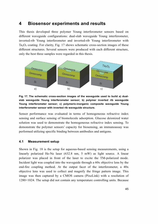
Shown in Fig. 18 is the setup for aqueous-based sensing measurements, using a
linearly polarized He-Ne laser (632.8 nm, 5 mW) as light source. A linear
polarizer was placed in front of the laser to excite the TM-polarized mode.
Incident light was coupled into the waveguide through a 60x objective lens by the
end-fire coupling method. At the output facet of the interferometer, a 40x
objective lens was used to collect and magnify the fringe pattern image. This
image was then captured by a CMOS camera (PixeLink) with a resolution of
1280×1024. The setup did not contain any temperature controlling units. Because
46
the experiments were carried out in an aqueous environment, a continuous-flow
syringe pump (OPAM Instruments) was used to deliver the analyte onto the
sensing window through a flow cell attached above the sensor chip. A silicone-
based gasket having an opening window with a volume of 10 µl was placed
between the sensing chip and the flow cell to prevent leakage of the liquid
samples at the interface of the chip and the cell.
Fig. 18. Biosensing measurement set-up.
Fringe pattern images were captured at a rate of 1Hz. To extract spatial changes in
the fringe pattern, representing phase changes of the interferogram, Matlab
software was used. This software implemented a 2D-FFT algorithm to calculate
the amplitude and phase spectrum of the fringe pattern image. The corresponding
phase of each image was extracted by looking up the value of the same frequency
showing the peak of the amplitude spectrum. Phase discontinuities were corrected
by adding multiples of ±2π when absolute jumps between consecutive extracted
phases were greater than or equal to the default jump tolerance of π radians. After
phase response extraction, Δneff could be derived using Equation (5).
4.2 Effect of water absorption in polymer waveguides
Due to their molecular structure, polymeric materials are permeable to water
vapour and able to absorb water molecules to a certain extent (Mark 2007). When
a polymer absorbs water molecules, its refractive index changes in response to
changes in density and molar refraction (Shioda et al. 2003). The whole process
of introducing water to the sensing window of the developed sensors is
summarized by the following description. When water is introduced to the
sensing window of a polymer waveguide sensor, an abrupt change of the phase
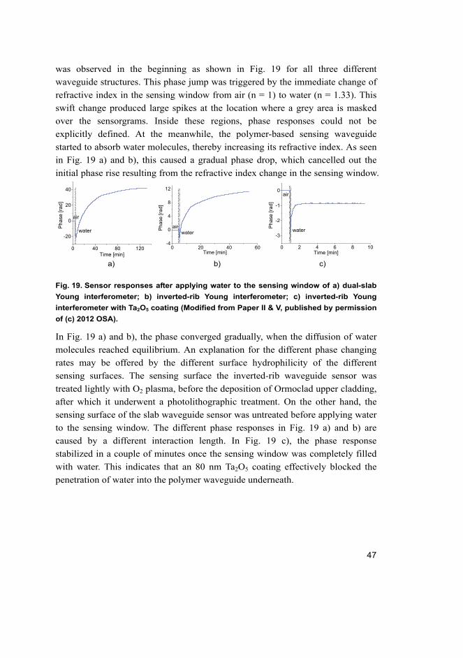
47
was observed in the beginning as shown in Fig. 19 for all three different
waveguide structures. This phase jump was triggered by the immediate change of
refractive index in the sensing window from air (n = 1) to water (n = 1.33). This
swift change produced large spikes at the location where a grey area is masked
over the sensorgrams. Inside these regions, phase responses could not be
explicitly defined. At the meanwhile, the polymer-based sensing waveguide
started to absorb water molecules, thereby increasing its refractive index. As seen
in Fig. 19 a) and b), this caused a gradual phase drop, which cancelled out the
initial phase rise resulting from the refractive index change in the sensing window.
0 40 80 120
-20
0
20
40
water
Ph
ase
[rad
]
Time [min]
air
0 20 40 60-4
0
4
8
12
Pha
se [
rad]
Time [min]
waterair
0 2 4 6 8 10
-3
-2
-1
0
Phase
[rad]
Time [min]
water
air
a) b) c)
Fig. 19. Sensor responses after applying water to the sensing window of a) dual-slab
Young interferometer; b) inverted-rib Young interferometer; c) inverted-rib Young
interferometer with Ta2O5 coating (Modified from Paper II & V, published by permission
of (c) 2012 OSA).
In Fig. 19 a) and b), the phase converged gradually, when the diffusion of water
molecules reached equilibrium. An explanation for the different phase changing
rates may be offered by the different surface hydrophilicity of the different
sensing surfaces. The sensing surface the inverted-rib waveguide sensor was
treated lightly with O2 plasma, before the deposition of Ormoclad upper cladding,
after which it underwent a photolithographic treatment. On the other hand, the
sensing surface of the slab waveguide sensor was untreated before applying water
to the sensing window. The different phase responses in Fig. 19 a) and b) are
caused by a different interaction length. In Fig. 19 c), the phase response
stabilized in a couple of minutes once the sensing window was completely filled
with water. This indicates that an 80 nm Ta2O5 coating effectively blocked the
penetration of water into the polymer waveguide underneath.
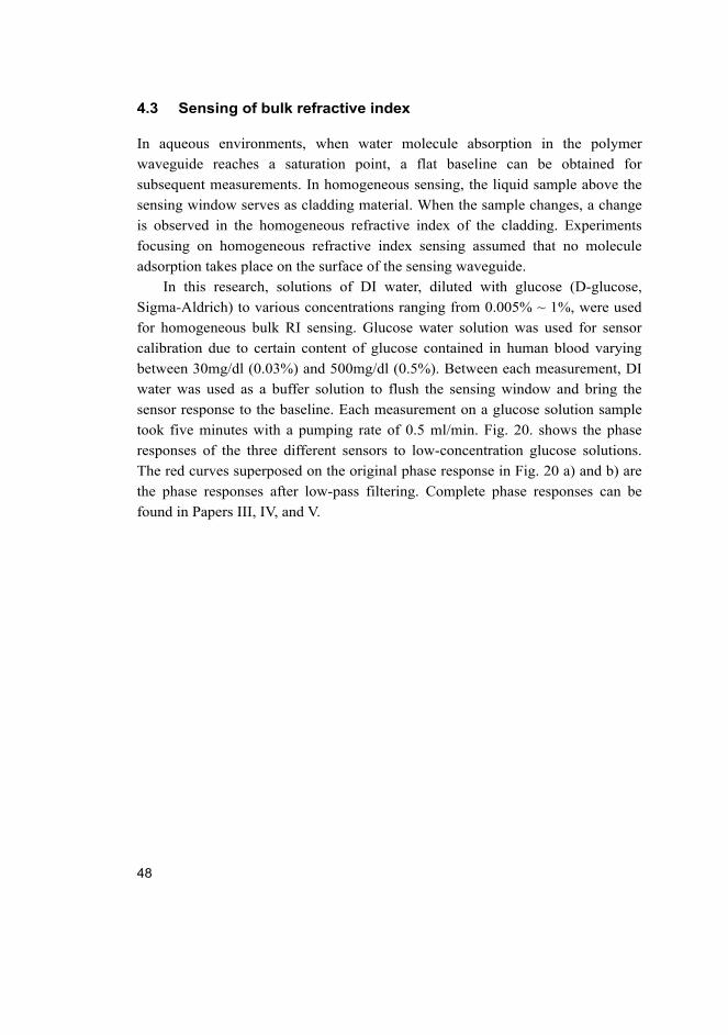
48
4.3 Sensing of bulk refractive index
In aqueous environments, when water molecule absorption in the polymer
waveguide reaches a saturation point, a flat baseline can be obtained for
subsequent measurements. In homogeneous sensing, the liquid sample above the
sensing window serves as cladding material. When the sample changes, a change
is observed in the homogeneous refractive index of the cladding. Experiments
focusing on homogeneous refractive index sensing assumed that no molecule
adsorption takes place on the surface of the sensing waveguide.
In this research, solutions of DI water, diluted with glucose (D-glucose,
Sigma-Aldrich) to various concentrations ranging from 0.005% ~ 1%, were used
for homogeneous bulk RI sensing. Glucose water solution was used for sensor
calibration due to certain content of glucose contained in human blood varying
between 30mg/dl (0.03%) and 500mg/dl (0.5%). Between each measurement, DI
water was used as a buffer solution to flush the sensing window and bring the
sensor response to the baseline. Each measurement on a glucose solution sample
took five minutes with a pumping rate of 0.5 ml/min. Fig. 20. shows the phase
responses of the three different sensors to low-concentration glucose solutions.
The red curves superposed on the original phase response in Fig. 20 a) and b) are
the phase responses after low-pass filtering. Complete phase responses can be
found in Papers III, IV, and V.
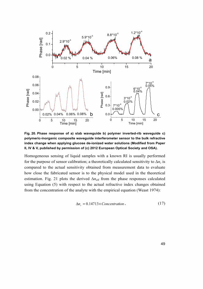
49
0 5 10 15 20
0.0
0.1
0.2
Pha
se [
rad]
Time [min]
0.02 %
2.9*10-5
0.04 % 0.06% 0.08 %
5.9*10-5 8.8*10-5 1.2*10-4
0 5 10 15 20
0.00
0.02
0.04
0.06
0.08
0.06% 0.08%0.04%
Pha
se [r
ad]
Time [min]
0.02%
0 5 10 15 20
0.0
0.3
0.6
0.9
Pha
se [
rad]
Time [min]
0.005%7*10-6
3*10-5
0.02%
0.04%6*10-5
7*10-5
0.05%
Fig. 20. Phase response of a) slab waveguide b) polymer inverted-rib waveguide c)
polymeric-inorganic composite waveguide interferometer sensor to the bulk refractive
index change when applying glucose de-ionized water solutions (Modified from Paper
II, IV & V, published by permission of (c) 2012 European Optical Society and OSA).
Homogeneous sensing of liquid samples with a known RI is usually performed
for the purpose of sensor calibration; a theoretically calculated sensitivity to Δnc is
compared to the actual sensitivity obtained from measurement data to evaluate
how close the fabricated sensor is to the physical model used in the theoretical
estimation. Fig. 21 plots the derived ∆neff from the phase responses calculated
using Equation (5) with respect to the actual refractive index changes obtained
from the concentration of the analyte with the empirical equation (Weast 1974):
ionConcentratnc ×=Δ 14713.0 , (17)
a
b c
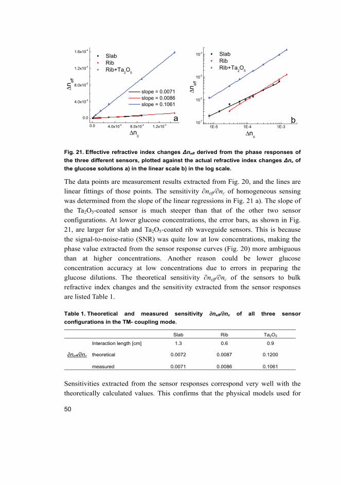
50
0.0 4.0x10⁻⁴ 8.0x10⁻⁴ 1.2x10⁻³
0.0
4.0x10⁻⁵
8.0x10⁻⁵
1.2x10⁻⁴
1.6x10⁻⁴
slope = 0.0071 slope = 0.0086 slope = 0.1061
Δnef
f
Δnc
Slab Rib Rib+Ta
2O
5
1E-5 1E-4 1E-310-7
10-6
10-5
10-4 Slab Rib Rib+Ta
2O
5
Δnef
f
Δnc
Fig. 21. Effective refractive index changes ∆neff derived from the phase responses of
the three different sensors, plotted against the actual refractive index changes ∆nc of
the glucose solutions a) in the linear scale b) in the log scale.
The data points are measurement results extracted from Fig. 20, and the lines are
linear fittings of those points. The sensitivity ∂neff/∂nc of homogeneous sensing
was determined from the slope of the linear regressions in Fig. 21 a). The slope of
the Ta2O5-coated sensor is much steeper than that of the other two sensor
configurations. At lower glucose concentrations, the error bars, as shown in Fig.
21, are larger for slab and Ta2O5-coated rib waveguide sensors. This is because
the signal-to-noise-ratio (SNR) was quite low at low concentrations, making the
phase value extracted from the sensor response curves (Fig. 20) more ambiguous
than at higher concentrations. Another reason could be lower glucose
concentration accuracy at low concentrations due to errors in preparing the
glucose dilutions. The theoretical sensitivity ∂neff/∂nc of the sensors to bulk
refractive index changes and the sensitivity extracted from the sensor responses
are listed Table 1.
Table 1. Theoretical and measured sensitivity ∂neff/∂nc of all three sensor
configurations in the TM- coupling mode.
Slab Rib Ta2O5
Interaction length [cm] 1.3 0.6 0.9
∂neff/∂nc theoretical 0.0072 0.0087 0.1200
measured 0.0071 0.0086 0.1061
Sensitivities extracted from the sensor responses correspond very well with the
theoretically calculated values. This confirms that the physical models used for
b a
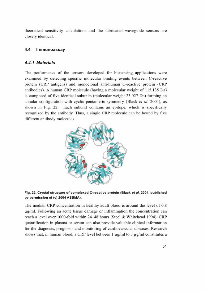
51
theoretical sensitivity calculations and the fabricated waveguide sensors are
closely identical.
4.4 Immunoassay
4.4.1 Materials
The performance of the sensors developed for biosensing applications were
examined by detecting specific molecular binding events between C-reactive
protein (CRP antigens) and monoclonal anti-human C-reactive protein (CRP
antibodies). A human CRP molecule (having a molecular weight of 115,135 Da)
is composed of five identical subunits (molecular weight 23,027 Da) forming an
annular configuration with cyclic pentameric symmetry (Black et al. 2004), as
shown in Fig. 22. Each subunit contains an epitope, which is specifically
recognized by the antibody. Thus, a single CRP molecule can be bound by five
different antibody molecules.
Fig. 22. Crystal structure of complexed C-reactive protein (Black et al. 2004, published
by permission of (c) 2004 ASBMA).
The median CRP concentration in healthy adult blood is around the level of 0.8
µg/ml. Following an acute tissue damage or inflammation the concentration can
reach a level over 1000-fold within 24–48 hours (Steel & Whitehead 1994). CRP
quantification in plasma or serum can also provide valuable clinical information
for the diagnosis, prognosis and monitoring of cardiovascular diseases. Research
shows that, in human blood, a CRP level between 1 µg/ml to 3 µg/ml constitutes a
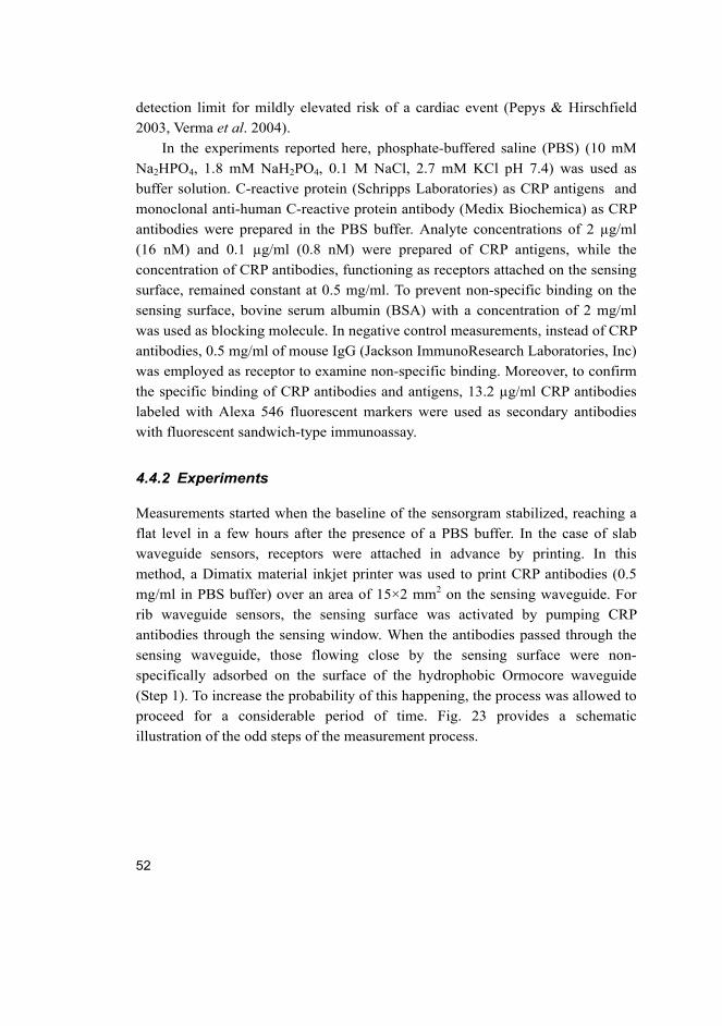
52
detection limit for mildly elevated risk of a cardiac event (Pepys & Hirschfield
2003, Verma et al. 2004).
In the experiments reported here, phosphate-buffered saline (PBS) (10 mM
Na2HPO4, 1.8 mM NaH2PO4, 0.1 M NaCl, 2.7 mM KCl pH 7.4) was used as
buffer solution. C-reactive protein (Schripps Laboratories) as CRP antigens and
monoclonal anti-human C-reactive protein antibody (Medix Biochemica) as CRP
antibodies were prepared in the PBS buffer. Analyte concentrations of 2 µg/ml
(16 nM) and 0.1 µg/ml (0.8 nM) were prepared of CRP antigens, while the
concentration of CRP antibodies, functioning as receptors attached on the sensing
surface, remained constant at 0.5 mg/ml. To prevent non-specific binding on the
sensing surface, bovine serum albumin (BSA) with a concentration of 2 mg/ml
was used as blocking molecule. In negative control measurements, instead of CRP
antibodies, 0.5 mg/ml of mouse IgG (Jackson ImmunoResearch Laboratories, Inc)
was employed as receptor to examine non-specific binding. Moreover, to confirm
the specific binding of CRP antibodies and antigens, 13.2 µg/ml CRP antibodies
labeled with Alexa 546 fluorescent markers were used as secondary antibodies
with fluorescent sandwich-type immunoassay.
4.4.2 Experiments
Measurements started when the baseline of the sensorgram stabilized, reaching a
flat level in a few hours after the presence of a PBS buffer. In the case of slab
waveguide sensors, receptors were attached in advance by printing. In this
method, a Dimatix material inkjet printer was used to print CRP antibodies (0.5
mg/ml in PBS buffer) over an area of 15×2 mm2 on the sensing waveguide. For
rib waveguide sensors, the sensing surface was activated by pumping CRP
antibodies through the sensing window. When the antibodies passed through the
sensing waveguide, those flowing close by the sensing surface were non-
specifically adsorbed on the surface of the hydrophobic Ormocore waveguide
(Step 1). To increase the probability of this happening, the process was allowed to
proceed for a considerable period of time. Fig. 23 provides a schematic
illustration of the odd steps of the measurement process.
53
Fig. 23. Illustration of the measurement performed to detect the surface adsorption of
biomolecules including specific binding between CRP molecules and their antibodies,
and the negative control measurement performed with mouse IgG. (Paper V, published
by permission of (c) 2012 OSA).
Even steps, not shown in this figure, consisted of rinsing with the PBS buffer after
each injection of biomolecules to flush away loosely attached and excessive
molecules. After surface activation with CRP antibodies, BSA was injected to
block any free spots on the waveguide surface to which CRP could bind
unspecifically (Step 3). After rinsing with PBS, CRP antigens were pumped
through the sensing window to bind specifically to the CRP antibodies on the
sensing surface (Step 5). In Step 7, secondary CRP antibodies, labeled with
fluorescent markers, were injected to confirm the measurement results under a
fluorescence stereomicroscope (SteREO Discovery.V8, Carl Zeiss). This was only
done after the injection of 0.1 µg/ml CRP analyte and after the negative control
on the slab waveguide and Ta2O5-coated rib waveguide sensor due to relatively
low surface mass densities involved in these experiments.
There are two reasons to use fluorescent-labelled secondary antibodies.
Firstly, at low concentrations, signal amplification may be needed. Since each
CRP antigen contains five identical epitopes, four will be left unoccupied when an
antigen binds to a CRP antibody on the sensing surface. By applying a high
concentration of secondary antibodies, all available epitopes can be expected to
become occupied, leading to amplified surface adsorption due to the comparable
molecular weight of the CRP antigens (115 kDa) and antibodies (150 kDa).
Secondly, non-specific binding needs to be verified on both Ormocore and Ta2O5-
based sensing surfaces.
For each of the three sensors, a negative control was performed with mouse
IgG as receptor, due to its low affinity toward CRP. The purpose was to ensure
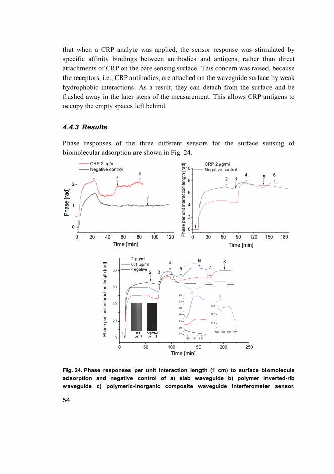
54
that when a CRP analyte was applied, the sensor response was stimulated by
specific affinity bindings between antibodies and antigens, rather than direct
attachments of CRP on the bare sensing surface. This concern was raised, because
the receptors, i.e., CRP antibodies, are attached on the waveguide surface by weak
hydrophobic interactions. As a result, they can detach from the surface and be
flushed away in the later steps of the measurement. This allows CRP antigens to
occupy the empty spaces left behind.
4.4.3 Results
Phase responses of the three different sensors for the surface sensing of
biomolecular adsorption are shown in Fig. 24.
0 20 40 60 80 100 120
0
1
2
Pha
se [
rad
]
Time [min]
CRP 2 μg/ml Negative control
6
3
45
7
0 30 60 90 120 150 180
0
2
4
6
8
10
1
Pha
se p
er u
nit i
nter
actio
n le
ngth
[rad
]
Time [min]
CRP 2 μg/ml Negative control
62 3
4 5
160 180 200 220
56,7
57,0
57,3
120 140 160
57
60
63
66
69
72
75
0 50 100 150 200 250
0
20
40
60
80
2 μg/ml 0.1 μg/ml negative
Pha
se p
er u
nit
inte
ract
ion
leng
th [r
ad]
Time [min]
1
6
2 3
47
8
5
Fig. 24. Phase responses per unit interaction length (1 cm) to surface biomolecule
adsorption and negative control of a) slab waveguide b) polymer inverted-rib
waveguide c) polymeric-inorganic composite waveguide interferometer sensor.
55
Images in the lower left corner are fluorescent microscopic images taken inside the
sensing window following a flow of secondary CRP antibodies. Numbers correspond
to the steps in the measurement process (Modified from Paper IV & V, published by
permission of (c) 2012 European Optical Society and OSA).
As shown in Fig. 24 a) for the slab waveguide sensor, the measurement started
with a BSA blocking step, since the attachment of CRP antibodies was prepared
in advance by inkjet printing. After rinsing, a clear rise of the phase occurred at
0.41 rad, following the injection of CRP antigens. In the negative control, no
obvious phase response followed the injection of CRP antigens and secondary
CRP antibodies, intended to increase signal amplification. The polymer rib
waveguide sensor, on the other hand, exhibited a large phase rise, when primary
antibodies of CRP and mouse IgG were injected. After BSA blocking, a clear
phase response was observed, following an injection of CRP antigens. After
flushing with PBS, 0.46 rad of additional phase increase remained. Similar to the
slab waveguide sensor, no signal rise was detected in the negative control. Finally,
measurements on the composite waveguide sensor began in the same manner as
those on the polymer rib waveguide sensor. However, phase responses obtained
from biomolecular adsorption were much greater. The remaining phase change
after PBS wash was about 9.1 rad and 2.3 rad for CRP analytes with a
concentration of 2 µg/ml and 0.1 µg/ml. Following the detection of 0.1 µg/ml
CRP analyte, a phase change of over 8 rad resulted from the injection of
secondary antibodies. The amplified phase response is due to multiple binding of
secondary antibodies to the primary antibody-antigen complexes. In the negative
control, only a small phase change was detected, representing minor nonspecific
binding. This nonspecific binding could only be detected by the composite
waveguide sensor, due to its higher sensitivity. Fluorescence microscopy images,
presented in Fig. 24, confirm that secondary antibodies attached well onto the
CRP antibody-activated surface, but not onto the sensing surface of the negative
control.
Taking into account the theoretical sensitivity of surface sensing, the actual
thickness growth of the adlayer can be calculated with the following equation:
ad
effeffad t
nnt
∂∂
Δ=Δ , (18)
The obtained layer thickness does not indicate exact molecular height, but an
average thickness taking account of molecular packing density. The
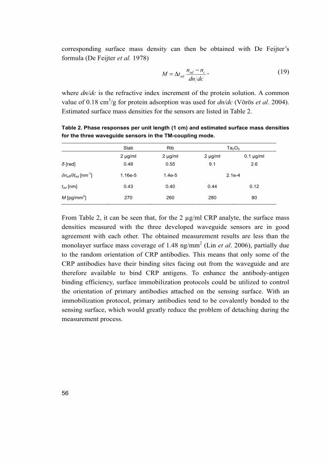
56
corresponding surface mass density can then be obtained with De Feijter’s
formula (De Feijter et al. 1978)
dcdn
nntM cad
ad
−Δ= , (19)
where dn/dc is the refractive index increment of the protein solution. A common
value of 0.18 cm3/g for protein adsorption was used for dn/dc (Vörös et al. 2004).
Estimated surface mass densities for the sensors are listed in Table 2.
Table 2. Phase responses per unit length (1 cm) and estimated surface mass densities
for the three waveguide sensors in the TM-coupling mode.
Slab Rib Ta2O5
2 µg/ml 2 µg/ml 2 µg/ml 0.1 µg/ml
δ [rad] 0.48 0.55 9.1 2.6
∂neff/∂tad [nm-1] 1.16e-5 1.4e-5 2.1e-4
tad [nm] 0.43 0.40 0.44 0.12
M [pg/mm2] 270 260 280 80
From Table 2, it can be seen that, for the 2 µg/ml CRP analyte, the surface mass
densities measured with the three developed waveguide sensors are in good
agreement with each other. The obtained measurement results are less than the
monolayer surface mass coverage of 1.48 ng/mm2 (Lin et al. 2006), partially due
to the random orientation of CRP antibodies. This means that only some of the
CRP antibodies have their binding sites facing out from the waveguide and are
therefore available to bind CRP antigens. To enhance the antibody-antigen
binding efficiency, surface immobilization protocols could be utilized to control
the orientation of primary antibodies attached on the sensing surface. With an
immobilization protocol, primary antibodies tend to be covalently bonded to the
sensing surface, which would greatly reduce the problem of detaching during the
measurement process.
57
5 Discussion
This section analyzes the influence of disturbance and noise on the measurement
system to determine the different waveguide sensors’ detection limit for bulk RI
sensing and sensing of biomolecule adsorption. Also the benefits and limitations
of the different sensing configurations are compared.
5.1 Measurement error analysis
Noise plays an important role in signal acquisition and processing. As the SNR
directly restricts the detection limit of the fabricated waveguide sensors, an
analysis of possible noise sources is neccessary be conducted. Noise that may
have an effect on the measurement results fall into the following categories:
mechanical, optical, environmental and electrical.
5.1.1 Mechanical noise
Two types of mechanical noise sources influence measurement results. Firstly,
there is vibration noise, which may originate from the floor, air fluctuations or
acoustic noise. It contributes to the measurement results by exciting differential
movement of the optical components (Selvin & Ha 2007). In this work,
differential movement refers to the relative movement between the waveguide
sensor and the objective lens when capturing fringe patterns (Fig. 18). Taking the
polymeric-inorganic composite waveguide sensor as an example, the period of the
generated fringe pattern is ~ 200 pixels. Using Equation (20), the actual spatial
period p can be estimated:
d
DP
λ= , (20)
where D = 2.5 mm is the distance from the sensor output facet to the collecting
objective lens, and d = 50 µm is the separation between the sensing and
referencing waveguide at the output facet. An actual spatial period of 32 µm is
found, corresponding to 5 µm for 1 radian in phase. Assuming that the generated
noise is entirely caused by vibration, the measured noise level of 0.003 radian
equals a relative movement of 15 nm between the waveguide sensor and the
objective lens.
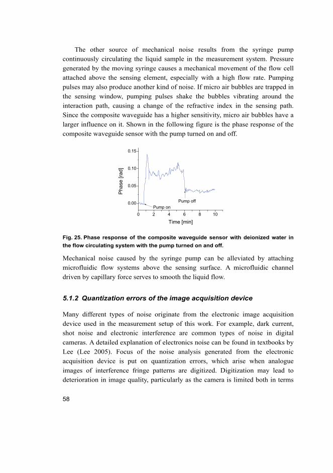
58
The other source of mechanical noise results from the syringe pump
continuously circulating the liquid sample in the measurement system. Pressure
generated by the moving syringe causes a mechanical movement of the flow cell
attached above the sensing element, especially with a high flow rate. Pumping
pulses may also produce another kind of noise. If micro air bubbles are trapped in
the sensing window, pumping pulses shake the bubbles vibrating around the
interaction path, causing a change of the refractive index in the sensing path.
Since the composite waveguide has a higher sensitivity, micro air bubbles have a
larger influence on it. Shown in the following figure is the phase response of the
composite waveguide sensor with the pump turned on and off.
0 2 4 6 8 10
0.00
0.05
0.10
0.15
Pump off
Pha
se [
rad]
Time [min]
Pump on
Fig. 25. Phase response of the composite waveguide sensor with deionized water in
the flow circulating system with the pump turned on and off.
Mechanical noise caused by the syringe pump can be alleviated by attaching
microfluidic flow systems above the sensing surface. A microfluidic channel
driven by capillary force serves to smooth the liquid flow.
5.1.2 Quantization errors of the image acquisition device
Many different types of noise originate from the electronic image acquisition
device used in the measurement setup of this work. For example, dark current,
shot noise and electronic interference are common types of noise in digital
cameras. A detailed explanation of electronics noise can be found in textbooks by
Lee (Lee 2005). Focus of the noise analysis generated from the electronic
acquisition device is put on quantization errors, which arise when analogue
images of interference fringe patterns are digitized. Digitization may lead to
deterioration in image quality, particularly as the camera is limited both in terms
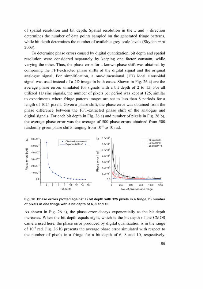
59
of spatial resolution and bit depth. Spatial resolution in the x and y direction
determines the number of data points sampled on the generated fringe patterns,
while bit depth determines the number of available grey-scale levels (Skydan et al.
2003).
To determine phase errors caused by digital quantization, bit depth and spatial
resolution were considered separately by keeping one factor constant, while
varying the other. Thus, the phase error for a known phase shift was obtained by
comparing the FFT-extracted phase shifts of the digital signal and the original
analogue signal. For simplification, a one-dimensional (1D) ideal sinusoidal
signal was used instead of a 2D image in both cases. Shown in Fig. 26 a) are the
average phase errors simulated for signals with a bit depth of 2 to 15. For all
utilized 1D sine signals, the number of pixels per period was kept at 125, similar
to experiments where fringe pattern images are set to less than 8 periods for a
length of 1024 pixels. Given a phase shift, the phase error was obtained from the
phase difference between the FFT-extracted phase shift of the analogue and
digital signals. For each bit depth in Fig. 26 a) and number of pixels in Fig. 26 b),
the average phase error was the average of 500 phase errors obtained from 500
randomly given phase shifts ranging from 10-4 to 10 rad.
0 2 4 6 8 10 12 14 16
0.0
1.0x10⁻³
2.0x10⁻³
3.0x10⁻³
4.0x10⁻³
5.0x10⁻³
6.0x10⁻³
Obtained phase error Exponential fit of
Pha
se e
rror
s [r
ad]
Bit depth
a
0 250 500 750 1000 1250
0.0
5.0x10⁻⁴
1.0x10⁻³
1.5x10⁻³
2.0x10⁻³
2.5x10⁻³
3.0x10⁻³
3.5x10⁻³
Pha
se e
rror
[ra
d]
No. of pixels in one fringe
Bit depth=6 Bit depth=8 Bit depth=10
b
Fig. 26. Phase errors plotted against a) bit depth with 125 pixels in a fringe, b) number
of pixels in one fringe with a bit depth of 6, 8 and 10.
As shown in Fig. 26 a), the phase error decays exponentially as the bit depth
increases. When the bit depth equals eight, which is the bit depth of the CMOS
camera used here, the phase error produced by digital quantization is in the range
of 10-4 rad. Fig. 26 b) presents the average phase error simulated with respect to
the number of pixels in a fringe for a bit depth of 6, 8 and 10, respectively.
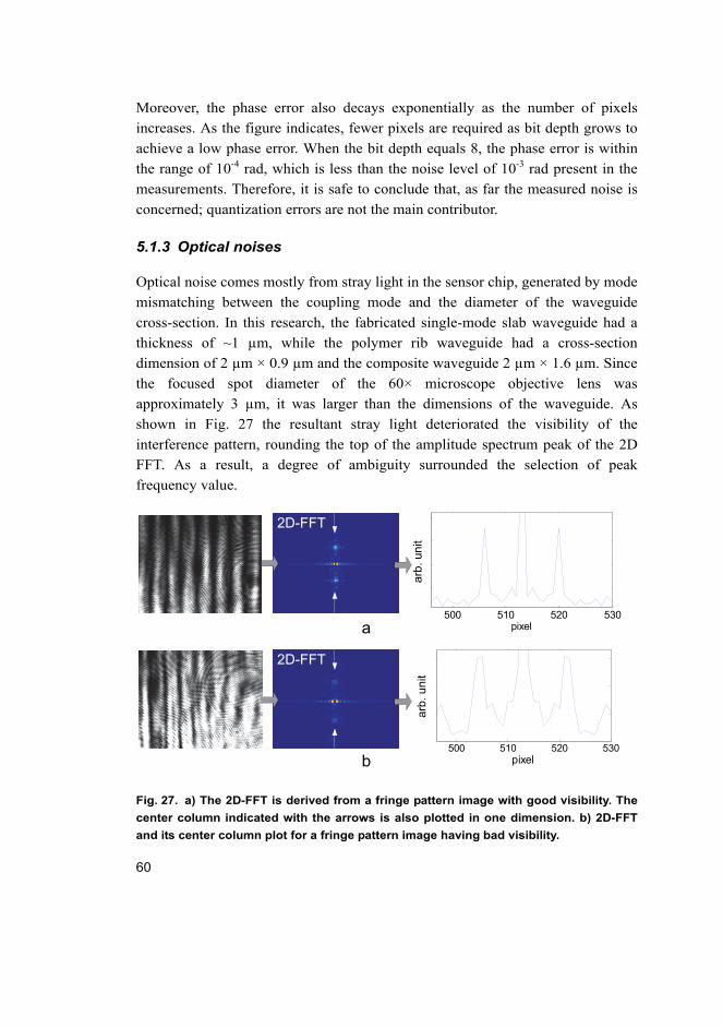
60
Moreover, the phase error also decays exponentially as the number of pixels
increases. As the figure indicates, fewer pixels are required as bit depth grows to
achieve a low phase error. When the bit depth equals 8, the phase error is within
the range of 10-4 rad, which is less than the noise level of 10-3 rad present in the
measurements. Therefore, it is safe to conclude that, as far the measured noise is
concerned; quantization errors are not the main contributor.
5.1.3 Optical noises
Optical noise comes mostly from stray light in the sensor chip, generated by mode
mismatching between the coupling mode and the diameter of the waveguide
cross-section. In this research, the fabricated single-mode slab waveguide had a
thickness of ~1 µm, while the polymer rib waveguide had a cross-section
dimension of 2 µm × 0.9 µm and the composite waveguide 2 µm × 1.6 µm. Since
the focused spot diameter of the 60× microscope objective lens was
approximately 3 µm, it was larger than the dimensions of the waveguide. As
shown in Fig. 27 the resultant stray light deteriorated the visibility of the
interference pattern, rounding the top of the amplitude spectrum peak of the 2D
FFT. As a result, a degree of ambiguity surrounded the selection of peak
frequency value.
500 510 520 530pixel
arb.
uni
t ar
b. u
nit
500 510 520 530
5
10
15
x 106
pixel
arb.
uni
tar
b. u
nit
a
b
2D-FFT
2D-FFT
Fig. 27. a) The 2D-FFT is derived from a fringe pattern image with good visibility. The
center column indicated with the arrows is also plotted in one dimension. b) 2D-FFT
and its center column plot for a fringe pattern image having bad visibility.
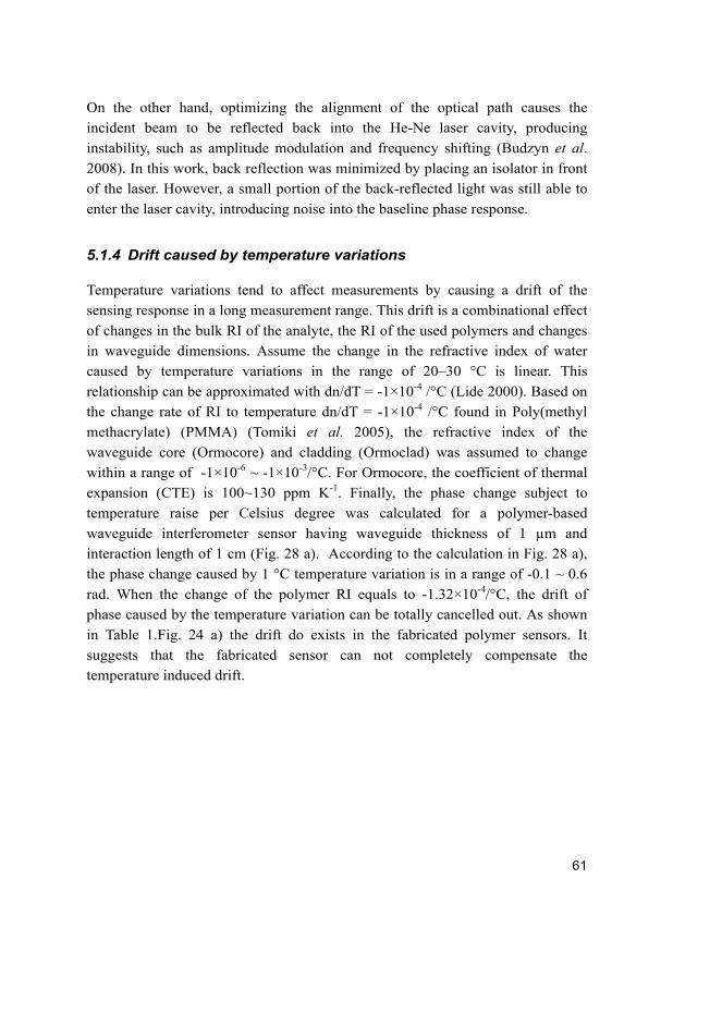
61
On the other hand, optimizing the alignment of the optical path causes the
incident beam to be reflected back into the He-Ne laser cavity, producing
instability, such as amplitude modulation and frequency shifting (Budzyn et al.
2008). In this work, back reflection was minimized by placing an isolator in front
of the laser. However, a small portion of the back-reflected light was still able to
enter the laser cavity, introducing noise into the baseline phase response.
5.1.4 Drift caused by temperature variations
Temperature variations tend to affect measurements by causing a drift of the
sensing response in a long measurement range. This drift is a combinational effect
of changes in the bulk RI of the analyte, the RI of the used polymers and changes
in waveguide dimensions. Assume the change in the refractive index of water
caused by temperature variations in the range of 20–30 °C is linear. This
relationship can be approximated with dn/dT = -1×10⁻⁴ /°C (Lide 2000). Based on
the change rate of RI to temperature dn/dT = -1×10⁻⁴ /°C found in Poly(methyl
methacrylate) (PMMA) (Tomiki et al. 2005), the refractive index of the
waveguide core (Ormocore) and cladding (Ormoclad) was assumed to change
within a range of -1×10⁻⁶ ~ -1×10⁻³/°C. For Ormocore, the coefficient of thermal
expansion (CTE) is 100~130 ppm K-1. Finally, the phase change subject to
temperature raise per Celsius degree was calculated for a polymer-based
waveguide interferometer sensor having waveguide thickness of 1 µm and
interaction length of 1 cm (Fig. 28 a). According to the calculation in Fig. 28 a),
the phase change caused by 1 °C temperature variation is in a range of -0.1 ~ 0.6
rad. When the change of the polymer RI equals to -1.32×10⁻⁴/°C, the drift of
phase caused by the temperature variation can be totally cancelled out. As shown
in Table 1.Fig. 24 a) the drift do exists in the fabricated polymer sensors. It
suggests that the fabricated sensor can not completely compensate the
temperature induced drift.
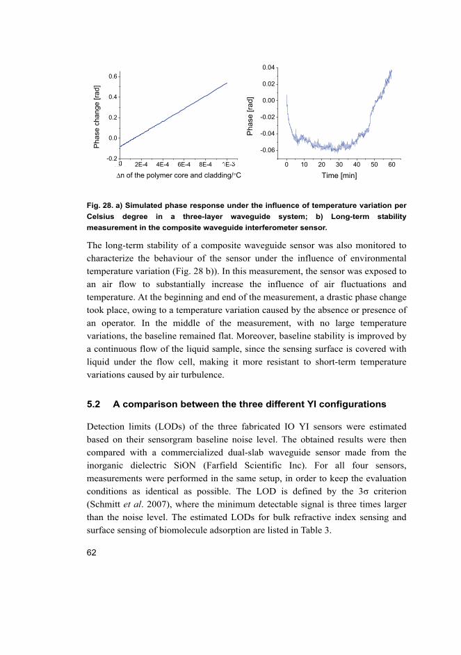
62
0E-4 2E-4 4E-4 6E-4 8E-4 10E-4-0.2
0.0
0.2
0.4
0.6
Pha
se c
hang
e [r
ad]
Δn of the polymer core and cladding/°C
0 10 20 30 40 50 60
-0.06
-0.04
-0.02
0.00
0.02
0.04
Pha
se [
rad]
Time [min]
Fig. 28. a) Simulated phase response under the influence of temperature variation per
Celsius degree in a three-layer waveguide system; b) Long-term stability
measurement in the composite waveguide interferometer sensor.
The long-term stability of a composite waveguide sensor was also monitored to
characterize the behaviour of the sensor under the influence of environmental
temperature variation (Fig. 28 b)). In this measurement, the sensor was exposed to
an air flow to substantially increase the influence of air fluctuations and
temperature. At the beginning and end of the measurement, a drastic phase change
took place, owing to a temperature variation caused by the absence or presence of
an operator. In the middle of the measurement, with no large temperature
variations, the baseline remained flat. Moreover, baseline stability is improved by
a continuous flow of the liquid sample, since the sensing surface is covered with
liquid under the flow cell, making it more resistant to short-term temperature
variations caused by air turbulence.
5.2 A comparison between the three different YI configurations
Detection limits (LODs) of the three fabricated IO YI sensors were estimated
based on their sensorgram baseline noise level. The obtained results were then
compared with a commercialized dual-slab waveguide sensor made from the
inorganic dielectric SiON (Farfield Scientific Inc). For all four sensors,
measurements were performed in the same setup, in order to keep the evaluation
conditions as identical as possible. The LOD is defined by the 3σ criterion
(Schmitt et al. 2007), where the minimum detectable signal is three times larger
than the noise level. The estimated LODs for bulk refractive index sensing and
surface sensing of biomolecule adsorption are listed in Table 3.
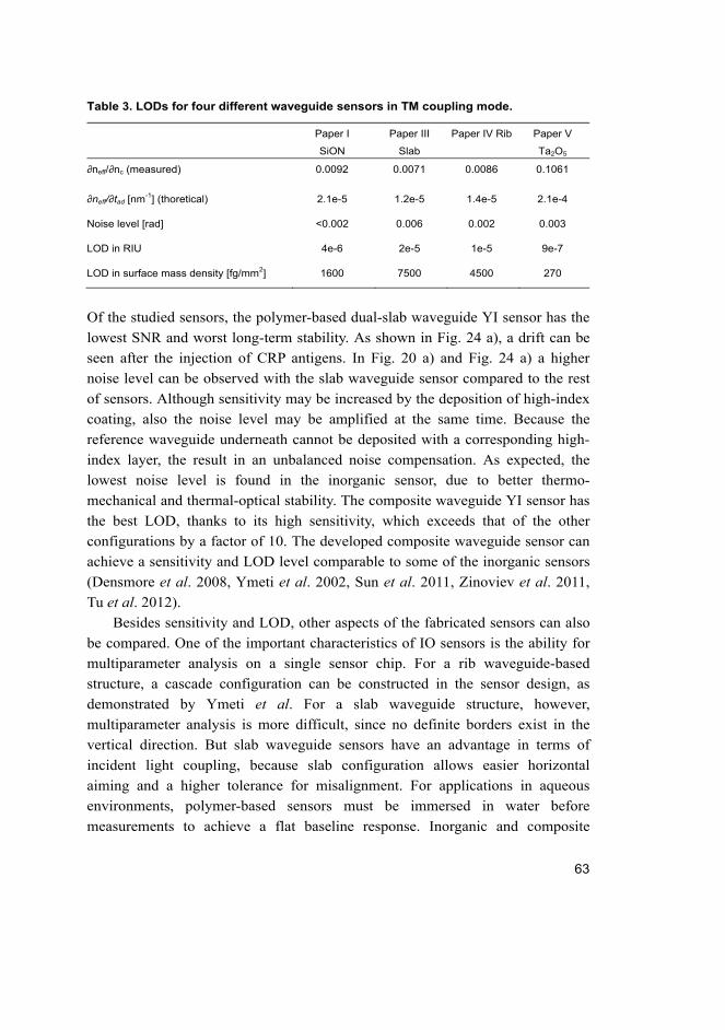
63
Table 3. LODs for four different waveguide sensors in TM coupling mode.
Paper I
SiON
Paper III
Slab
Paper IV Rib Paper V
Ta2O5
∂neff/∂nc (measured) 0.0092 0.0071 0.0086 0.1061
∂neff/∂tad [nm-1] (thoretical) 2.1e-5 1.2e-5 1.4e-5 2.1e-4
Noise level [rad] <0.002 0.006 0.002 0.003
LOD in RIU 4e-6 2e-5 1e-5 9e-7
LOD in surface mass density [fg/mm2] 1600 7500 4500 270
Of the studied sensors, the polymer-based dual-slab waveguide YI sensor has the
lowest SNR and worst long-term stability. As shown in Fig. 24 a), a drift can be
seen after the injection of CRP antigens. In Fig. 20 a) and Fig. 24 a) a higher
noise level can be observed with the slab waveguide sensor compared to the rest
of sensors. Although sensitivity may be increased by the deposition of high-index
coating, also the noise level may be amplified at the same time. Because the
reference waveguide underneath cannot be deposited with a corresponding high-
index layer, the result in an unbalanced noise compensation. As expected, the
lowest noise level is found in the inorganic sensor, due to better thermo-
mechanical and thermal-optical stability. The composite waveguide YI sensor has
the best LOD, thanks to its high sensitivity, which exceeds that of the other
configurations by a factor of 10. The developed composite waveguide sensor can
achieve a sensitivity and LOD level comparable to some of the inorganic sensors
(Densmore et al. 2008, Ymeti et al. 2002, Sun et al. 2011, Zinoviev et al. 2011,
Tu et al. 2012).
Besides sensitivity and LOD, other aspects of the fabricated sensors can also
be compared. One of the important characteristics of IO sensors is the ability for
multiparameter analysis on a single sensor chip. For a rib waveguide-based
structure, a cascade configuration can be constructed in the sensor design, as
demonstrated by Ymeti et al. For a slab waveguide structure, however,
multiparameter analysis is more difficult, since no definite borders exist in the
vertical direction. But slab waveguide sensors have an advantage in terms of
incident light coupling, because slab configuration allows easier horizontal
aiming and a higher tolerance for misalignment. For applications in aqueous
environments, polymer-based sensors must be immersed in water before
measurements to achieve a flat baseline response. Inorganic and composite
64
waveguide sensors, on the other hand, do not require such advance preparations.
In terms of fabrication, inorganic slab waveguides need consecutive depositions
of SiON layers by a chemical vapor deposition (CVD) system, while polymer-
based waveguide sensors only require spin coating and imprinting. For the
composite waveguide sensor, only one inorganic high-index layer needs to be
deposited by sputtering at near-room temperature. Therefore, the fabrication of
polymer-based waveguide sensors, especially rib waveguide sensors, can be less
expensive and less time consuming.
Having evaluated all the aspects mentioned above, we may conclude that, of
all the developed sensors, the composite rib waveguide configuration has the most
favourable performance characteristics and a relatively simple fabrication process.
In addition, inorganic Ta2O5 coating can effectively block water penetration into
the polymer waveguide. This stabilizes the sensing response immediately after the
application of an aqueous solution, making the sensor ready for measurements.
5.3 Future work
There are several ways of improving the performance of the developed sensors.
For the detection of biomolecular binding events, the receptors can be
immobilized firmly on the sensing surface through, for example, covalent
bonding to minimize the risk of receptor detachment. To improve the system’s
SNR, integrated microfluidic channels could be used to alleviate mechanical
noise caused by the continuous syringe pump. Moreover, multiparameter sensing
could be realized by a higher level integration of rib waveguide YI sensors on a
single sensor chip. It would extend the range of references to the sensing system
and further improve noise compensation.
The next stage of the current work involves the adaption of the fabrication
process of rib waveguide YI sensors to the roll-to-roll printing technique that is
compatible for high volume production. In the future, the development of a fully
integrated lab-on-a-chip biosensor comprising the developed waveguide
interferometer together with a compact light source, a polarizer, and a detector
would be an eventual solution for a compact biosensor.
65
6 Summary
The main ambition of this thesis was to develop low-cost disposable IO
biosensors compatible for industrial mass-production. Polymers have been used
as fundamental materials in sensor development due to their good optical
properties, versatile processability and relatively low cost. This thesis used a
series of UV-curable organic and inorganic hybrid materials known as Ormocer
for sensor fabrication, largely owing to their comparatively good chemical and
thermal stability.
Three types of IO YI sensors with different waveguide configurations were
developed here: polymer dual-slab waveguide sensors, polymer inverted-rib
waveguide sensors and composite waveguide sensors based on the inverted-rib
waveguide structure with Ta2O5 coating. These three configurations were selected
to enhance the capabilities of the sensor prototype by enabling a new compact
structure, a simplified fabrication process and enhanced sensitivity.
Theoretical sensitivities were analyzed for homogenous refractive index
sensing and surface biomolecule adsorption. The results confirmed that an 80 nm
Ta2O5 layer deposited on a polymer waveguide improved its sensitivity in the
TM-coupling mode by over 40 times. Also propagation modes in each waveguide
configuration were simulated and single mode sensing was assured for all three
configurations.
Considering the configuration of each type of the sensors separately, we find
that the dual-slab waveguide IO YI sensors can be fabricated by multiple spin-
coating processes. Moreover, compared to rib waveguides, it allows easier
coupling of incident light with a greater tolerance for misalignment. For the
inverted-rib waveguide sensors, a very simply fabrication process, compatible to
roll-to-roll printing technique, was developed. Utilizing UV-imprinting, the
inverted-rib waveguide sensor can be fabricated in just two main steps:
patterning/imprinting the undercladding of the waveguide and spin-coating its
core. Being totally RIE-free, this method simplifies the fabrication process and
eliminates the risk of increased waveguide surface roughness, which could cause
additional scattering loss. The composite waveguide sensors, based on the
inverted-rib waveguide structure with an additional high RI Ta2O5 coating, enable
a simple, low-cost fabrication process with a minimum number of inorganic layer
depositions. Furthermore, the high-index inorganic layer serves not only to
improve sensitivity but, in aqueous environments, it also prevents the absorption
of water molecules in the polymer waveguide.
66
The developed sensors were evaluated in glucose DI-water for homogenous
bulk RI sensing and in an immunoassay for surface sensing of protein adsorption.
All the tested sensors fulfilled these functions in both sensing mechanisms but,
with a LOD of 9 ×10⁻⁷ RIU and 270 fg/mm2 for surface mass density, the best
results were achieved by composite waveguide sensors. A simple fabrication
procedure and high sensitivity place Ta2O5-deposited polymeric-inorganic
composite waveguide YI sensors high on the list of disposable low-cost
biosensors suitable for mass production.
67
References
Agnarsson, B, Halldorsson, J, Arnfinnsdottir, N., Ingthorsson, S, Gudjonsson, T, Leosson, K. Fabrication of planar polymer waveguides for evanescent-wave sensing in aqueous environments. Microelectron Eng 87 (1): 56–61.
Black S, Kushner I & Samols D (2004) C-reactive Protein. J Biol Chem 279: 48487–48490. Brandenburg A, Krauter R, Künzel C, Stefan M & Schulte H (2000) Interferometric sensor
for detection of surface-bound bioreactions. Appl Opt 39(34): 6396–6405. Bruck R, Melnik E, Muellner P, Hainberger R & Lämmerhofer M (2011) Integrated
polymer-based Mach-Zehnder interferometer label-free streptavidin biosensor compatible with injection molding. Biosens Bioelectron 26: 3832–3837.
Buestrich R, Kahlenberg F, Popall M, Dannberg P, Müller-Fiedler R & Rösch O (2001) ORMOCERs for optical interconnection technology. J Sol-Gel Sci Technol 20 (2): 181–186.
Budzyn G & Rzepka J (2008) Back-reflection effects in a frequency-stabilized two-mode He–Ne laser. Opt Commun 281(22): 5592–5595.
Cassidy DR & Cross GH (2007) Picometer Resolution Wavelength Tracking in the C -Band Using an InP–InGaAsP Dual-Slab Interferometer. IEEE Photon. Technol Lett 19(14): 1075–1077.
Cha H-Y, Choi H-G, Nam J-D, Lee Y, Cho SM, Lee E-S, Lee J-K & Chung C-H (2004) Fabrication of all-polymer micro-DMFCs using UV-sensitive photoresist, Electrochimica Acta 50 (2–3): 795–799.
Chang-Yen D, Eich R & Gale B (2005) A monolithic PDMS waveguide system fabricated using soft-lithography techniques. J Lightwave Technol 23(6): 2088–2093.
Chao CY, Fung W & Guo LJ (2006) Polymer microring resonators for biochemical sensing applications. IEEE J. Sel. Top. Quant Electron 12(1): 134–142.
Chen RJ, Choi HC, Bangsaruntip S, Yenilmez E, Tang X, Wang Q, Chang YL & Dai H (2004) An investigation of the mechanisms of electronic sensing of protein adsorption on carbon nanotube devices. J Am Chem Soc 126 (5): 1563–1568.
Cooper MA (2009) Label free biosensors techniques and applications, Cambridge University Press, UK.
Cross GH, Ren Y & Freeman NJ (1999) Young's fringes from vertically integrated slab waveguides: applications to humidity sensing. J Appl Phys 86: 6483.
Cross GH, Reeves AA, Brand S, Popplewell JF, Peel LL, Swann MJ & Freeman NJ (2003) A new quantitative optical biosensor for protein characterization. Biosens. Bioelectron. 19: 383–390.
De Feijter JA, Benjamins J, Veer FA (1978) Ellipsometry as a tool to study the adsorption behaviour of synthetic and biopolymers at the air–water interface. Biopolymers 17: 1759–1772.
Densmore A, Xu D, Janz S, Waldron P, Mischki T, Lopinski G, Delâe A, Lapointe J, Cheben P, Lamontagne B & J. Schmid (2008) Spiral-path high-sensitivity silicon photonic wire molecular sensor with temperature-independent response. Opt Lett 33: 596–598.
68
Eldada L, Xu C, Stengel KMT, Shacklette LW & Yardley JT (1996) Laser-fabricated low-loss single-mode raised-rib waveguiding devices in polymers. J Lightwave Technol 14(7): 1704–1713.
Eldada L & Shacklette LW (2000) Advances in polymer integrated optics. IEEE J. Sel. Top Quant 6(1): 54–68.
Fan X, White IM, Shopova SI, Zhu H, Suter JD & Yuze Sun (2008) Sensitive optical biosensors for unlabeled targets: A review. Analytica Chimica Acta 620(1–2): 8–26.
George AJT, French RR & Glennie MJ (1995) Measurement of kinetic binding constants of a panel of anti-saporin antibodies using a resonant mirror biosensor. J Immunol Methods 183(1): 51–63.
Guo LJ (2007) Nanoimprint lithography methods and material requirements. Adv Mater 19: 495–513. Hariharan P (2003) Optical interferometry. 2nd edition Academic press, Australia. Heckele M, Schomburg WK (2004) Review on micro molding of thermoplastic polymers.
J Micromech Microeng 14 (3): R1–R14. Hiltunen J, Hiltunen M, Puustinen J, Lappalainen J & Karioja P (2009) Fabrication of
optical waveguides by imprinting: Usage of positive tone resist as a mould for UV-curable polymer. Opt Express 17: 22813–22822.
Homola J, Yee SS, Gauglitz G (1999) Surface plasmon resonance sensors: review. Sensor Actuat B-Chem 54 (1): 3–15.
Horvath R, Pedersen HC, Skivesen N, Svanberg C & Larsen NB (2005) Fabrication of reverse symmetry polymer waveguide sensor chips on nanoporous substrates using dip-floating. J Micromech Microeng 15 (6): 1260–1264.
Houbertz R, Domann G, Cronauer C, Schmitt A, Martin H, Park JU, Fröhlich L, Buestrich R, Popall M, Streppel U, Dannberg P, Wächter C & Bräuer A (2003) Inorganic-organic hybrid materials for application in optical devices. Thin Solid Films 442 (1–2): 194–200.
Hsu SM, Raine L, Fanger H (1981) A comparative study of the peroxidase-antiperoxidase method and an avidin-biotin complex method for studying polypeptide hormones with radioimmunoassay antibodies. Am J Clin Pathol 75(5): 734–8.
Hunsperger RG (2009) Integrated optics theory and technology. 6th edition, Springer. Kawano K & Kitoh T (2001) Introduction to Optical Waveguide Analysis. Wiley. Kim GD, Son GS, Lee HS, Kim KD & Lee SS (2008) Integrated photonic glucose
biosensor using a vertically coupled microring resonator in polymers. Opt Commun 281(18): 4644–4647.
Kim JW, Kim KJ, Yi JA & Oh MC (2010) Polymer waveguide label-free biosensors with enhanced sensitivity by incorporating low-refractive-index polymers. IEEE J Sel Top Quant Electron 16(4): 973–980.
Kozma P, Hámori A, Kurunczi S, Cottier K & Horvath R (2011) Grating coupled optical waveguide interferometer for label-free biosensing. Sensor Actuat. B-Chem 155: 446–450 (2011).
Ksendzov A & Lin Y (2005) Integrated optics ring-resonator sensors for protein detection. Opt Lett 30 (24): 3344–3346.
69
Kuo CW, Shiu JY, Chen P & Somorjai GA (2003) Fabrication of size-tunable large-area periodic silicon nanopillar arrays with sub-10 nm resolution. J Phys Chem B 107: 9950–9953.
Kwon SW, Yang WS, Lee HM, Kim WK, Son GS, Yoon DH, Lee SD & Lee HY (2009) The fabrication of polymer-based evanescent optical waveguide for biosensing. Appl. Surf Sci 255(10): 5466–5470.
Lambeck PV (2006) Integrated optical sensors for the chemical domain. Meas Sci Technol 17: R93–R116.
Lee HC (2005) Introduction to Color Imaging Science. Cambridge University Press, UK. Lide DR (2000–2001) Handbook of Chemistry and Physics. CRC Press LLC. Lifante G (2003) Integrated photonics: fundamentals. Wiley. Ligler FS & Taitt CAR (Eds.) (2002) Optical biosensors: present and future. 1st Edition
Elsevier, Amsterdam The Netherlands. Lin S, Lee CK, Wang YM, Huang LS, Lin YH, Lee SY, Sheu BC & Hsu SM (2006)
Measurement of dimensions of pentagonal doughnut-shaped C-reactive protein using an atomic force microscope and a dual polarisation interferometric biosensor. Biosens Bioelectron 22(2): 323–327.
Lukosz W (1991) Principles and sensitivities of integrated optical and surface plasmon sensors for direct affinity sensing and immunosensing. Biosensors and Bioelectronics 6: 215–225.
Länge K, Rapp BE & Rapp M (2008) Surface acoustic wave biosensors: a review. Anal. Bioanal Chem 391(5): 1509–1519.
Ma H, Jen AKY, Dalton LR (2002) Polymer-based optical waveguides: materials, processing, and devices. Adv Mat 14(19): 1339–1365.
Mark JE (2007) Physical properties of polymers handbook. 2nd edition Springer New York. Mukundan H, Anderson AS, Grace WK, Grace KM, Hartman N, Martinez JS & Swanson
BI (2009) Waveguide-Based Biosensors for Pathogen Detection. Sensors 9(7): 5783–5809.
Narayanaswamy R & Wolfbeis OS (2004) Optical Sensors: industrial, environmental and diagnostic applications. Springer, New York.
Oh MC, Kim KJ, Lee JH, Chen HX & Koh KN (2006) Polymeric waveguide biosensors with calixarene monolayer for detecting potassium ion concentration. Appl Phys Lett 89 (25): 251104.
Paloczi GT (2005) Polymer integrated optics: Device architectures and fabrication methods. Ph.D Thesis, California Institute of Technology Pasadena, California.
Pearce SJ, Charlton MDB, Hiltunen J, Puustinen J, Lappalainen J & Wilkinson JS (2012) Structural characteristics and optical properties of plasma assisted reactive magnetron sputtered dielectric thin films for planar waveguiding applications. Surf Coat Tech 206 (23): 4930–4939.
Pepys MB & Hirschfield GM (2003) C-reactive protein: a critical update. J Clin Invest 111: 1805–1812.
Prasad PN (2003) Introduction to biophotonics. Wiley-Interscience.
70
Prieto F, Sepúlveda B, Calle A, Llobera A, Domı ́nguez C & Lechuga LM (2003) Integrated Mach–Zehnder interferometer based on ARROW structures for biosensor applications. Sensor Actuat B-Chem 92(1–2): 151–158.
Qi ZM., Zhao S, Chen F & Xia S (2009) Integrated Young interferometer sensor with a channel-planar composite waveguide sensing arm. Opt Lett 34 (14): 2213–2215.
Ray S, Mehta G & Srivastava S (2010) Label-free detection techniques for protein microarrays: prospects, merits and challenges. Proteomics 10(4): 731–48.
Reed GT & Knights AP (2004) Silicon photonics. Wiley. Ricard-Blum S, Peel LL, Ruggiero F & Freeman NJ (2006) Dual polarization
interferometry characterization of carbohydrate–protein interactions. Anal Biochem 352(2): 252–259.
Schmitt K, Oehse K, Sulz G & Hoffmann C (2008) Evanescent field sensors based on tantalum pentoxide waveguides – a review. Sensors 8: 711–738.
Schmitt K, Schirmer B, Hoffmann C, Brandenburg A & Meyrueis P (2007) Interferometric biosensor based on planar optical waveguide sensor chips for label-free detection of surface bound bioreactions. Biosens. Bioelectron 22: 2591–2597.
Selvin PR & Ha T (2007) Single –molecule techniques: a laboratory manual. 1st edition, Cold Spring Harbor Laboratory Press, New York.
Shew BY, Cheng YC & Tsai YH (2008) Monolithic SU-8 micro-interferometer for biochemical detections. Sensor Actuat A-Phys 141(2): 299–306.
Shioda T, Takamatsu N, Suzuki K, Shichijyo S (2003) Influence of water sorption on refractive index of fluorinated polymide. Polymer 44: 137–142.
Skivesen N, Têtu A, Kristensen M, Kjems J, Frandsen LH, Borel PI (2007) Photonic-crystal waveguide biosensor. Opt Express 15 (6): 3169–3176.
Skydan OA, Lilley F, Lalor MJ & Burton DR (2003) Quantization error of CCD cameras and their influence on phase calculation in fringe pattern analysis. Appl. Opt. 42(26): 5302–5307.
Steel DM & Whitehead AS (1994) The major acute phase reactants: C-reactive protein, serum amyloid P component and serum amyloid A protein. Immunol Today 15(2): 81–88.
Streppel U, Dannberg P, Wächter C, Bräuer A, Fröhlich L, Houbertz R & Popall M (2003) New wafer-scale fabrication method for stacked optical waveguide interconnects and 3D micro-optic structures using photoresponsive (inorganic–organic hybrid) polymers. Opt Mater 21: 475–483.
Sun B, Chen M, Zhang Y, Yang J, Yao J & Cui H (2011) Microstructured-core photonic-crystal fiber for ultra-sensitive refractive index sensing. Opt Express 19(5): 4091–4100.
Taitt CR, Anderson GP & Ligler FS (2005) Evanescent wave fluorescence biosensors. Biosens Bioelectron 20: 2470–2487.
Tiefenthaler K & Lukosz W (1989) Sensitivity of grating couplers as integrated-optical chemical sensors. J Opt Soc Am B 6(2): 209–220.
Tien P (1971) Light Waves in Thin Films and Integrated Optics. Appl. Opt. 10: 2395–2413.
71
Tomiki M, Kurihara N, Sugihara O & and Okamoto N (2005) A New Method for Accurately Measuring Temperature Dependence of Refractive Index. Optical Review 12(2): 97–100.
Tu X, Song J, Liow T, Park M, Yiying J, Kee J, Yu M & Lo G (2012) Thermal independent Silicon-Nitride slot waveguide biosensor with high sensitivity. Opt Express 20(3) 2640–2648.
Unger MA, Chou H-P, Thorsen T, Scherer A & Quake SR (2000) Monolithic microfabricated valves and pumps by multilayer soft lithography. Science 288 (5463): 113–116.
Usui M, Hikita M, Watanabe T, Amano M, Sugawara S, Hayashida S & Imamura S (1996) Low-loss passive polymer optical waveguides with high environmental stability. J. Lightwave Technol 14(10):2338–2343.
Verma S, Szmitko PE & Yeh ETH (2004) C-reactive protein: structure affects function. Circulation 109: 1914–1917. Vörös J (2004) The density and refractive index of adsorbing protein layers. Biophys J 87(1): 553–561. Vörös J, Ramsden JJ, Csúcs G, Szendrő I, De Paul SM, Textor M & Spencer ND (2002)
Optical grating coupler biosensors. Biomaterials 23(17): 3699–3710. Wang J (2006) Electrochemical biosensors: Towards point-of-care cancer diagnostics.
Biosens Bioelectron 21: 1887–1892. Weast RC (1974) Handbook of Chemistry and Physics. 55th ed. CRC Press Cleveland,
Ohio, USA. Ymeti A, Kanger JS, Greve J, Besselink GAJ, Lambeck PV, Wijn R & Heideman RG
(2005) Integration of microfluidics with a four-channel integrated optical young interferometer immunosensor. Biosens Bioelectron 20: 1417–1421.
Ymeti A, Kanger JS, Wijn R, Lambeck PV & Greve J (2002) Development of a multichannel integrated interferometer immunosensor. Sens Actuators B: Chem 83(1–3): 1–7.
Zinoviev K, Gonzáez-Guerrero A, Domíguez C & Lechuga L (2011) Integrated Bimodal Waveguide Interferometric Biosensor for Label-Free Analysis. J Lightwave Technol 29(13): 1926–1930.

72
73
Original Papers
I Wang M, Uusitalo S, Määttälä M, Myllylä R & Känsäkoski M (2008) Integrated dual-slab waveguide interferometer for glucose concentration detection in the physiological range. Proc SPIE 7003: 70031N-1-10. DOI: 10.1117/12.780184.
II Wang M, Uusitalo S, Liedert C, Hiltunen J, Hakalahti L & Myllylä R (2012) Polymeric dual-slab waveguide interferometer for biochemical sensing applications. Appl Opt 51: 1886–1893.
III Wang M, Hiltunen J, Uusitalo S, Puustinen J, Lappalainen J, Karioja P & Myllylä R (2011) Fabrication of optical inverted-rib waveguides using UV-imprinting. Microeletron Eng 88(2): 175–178.
IV Wang M, Hiltunen J, Liedert C, Hakalahti L & Myllylä R (2012) An integrated Young interferometer based on UV-imprinted polymer waveguides for label-free biosensing applications. J Europ Opt Soc Rap. Public. 7: 12019.
V Wang M, Hiltunen J, Liedert C, Pearce S, Charlton M, Hakalahti L, Karioja P & Myllylä R (2012) Highly sensitive biosensor based on UV-imprinted layered polymeric–inorganic composite waveguides. Opt Express 20: 20309–20317.
Reprinted with permission from SPIE (I) OSA (II, V) Elsevier (III) and European
Optical Society (IV).
Original publications are not included in the electronic version of the dissertation.

74
A C T A U N I V E R S I T A T I S O U L U E N S I S
Book orders:Granum: Virtual book storehttp://granum.uta.fi/granum/
S E R I E S C T E C H N I C A
416. Isoherranen, Ville (2012) Strategy analysis frameworks for strategy orientationand focus
417. Ruuska, Jari (2012) Special measurements and control models for a basic oxygenfurnace (BOF)
418. Kropsu-Vehkaperä, Hanna (2012) Enhancing understanding of company-wideproduct data management in ICT companies
419. Hietakangas, Simo (2012) Design methods and considerations of supplymodulated switched RF power amplifiers
420. Davidyuk, Oleg (2012) Automated and interactive composition of ubiquitousapplications
421. Suutala, Jaakko (2012) Learning discriminative models from structured multi-sensor data for human context recognition
422. Lorenzo Veiga, Beatriz (2012) New network paradigms for future multihopcellular systems
423. Ketonen, Johanna (2012) Equalization and channel estimation algorithms andimplementations for cellular MIMO-OFDM downlink
424. Macagnano, Davide (2012) Multitarget localization and tracking : Active andpassive solutions
425. Körkkö, Mika (2012) On the analysis of ink content in recycled pulps
426. Kukka, Hannu (2012) Case studies in human information behaviour in smarturban spaces
427. Koivukangas, Tapani (2012) Methods for determination of the accuracy of surgicalguidance devices : A study in the region of neurosurgical interest
428. Landaburu-Aguirre, Junkal (2012) Micellar-enhanced ultrafiltration for theremoval of heavy metals from phosphorous-rich wastewaters : From end-of-pipeto clean technology
429. Myllymäki, Sami (2012) Capacitive antenna sensor for user proximity recognition
430. Jansson, Jussi-Pekka (2012) A stabilized multi-channel CMOS time-to-digitalconverter based on a low frequency reference
431. Soini, Jaakko (2012) Effects of environmental variations in Escherichia colifermentations
C432etukansi.fm Page 2 Friday, October 26, 2012 12:55 PM

ABCDEFG
UNIVERS ITY OF OULU P.O.B . 7500 F I -90014 UNIVERS ITY OF OULU F INLAND
A C T A U N I V E R S I T A T I S O U L U E N S I S
S E R I E S E D I T O R S
SCIENTIAE RERUM NATURALIUM
HUMANIORA
TECHNICA
MEDICA
SCIENTIAE RERUM SOCIALIUM
SCRIPTA ACADEMICA
OECONOMICA
EDITOR IN CHIEF
PUBLICATIONS EDITOR
Senior Assistant Jorma Arhippainen
University Lecturer Santeri Palviainen
Professor Hannu Heusala
Professor Olli Vuolteenaho
University Lecturer Hannu Heikkinen
Director Sinikka Eskelinen
Professor Jari Juga
Professor Olli Vuolteenaho
Publications Editor Kirsti Nurkkala
ISBN 978-951-42-9963-6 (Paperback)ISBN 978-951-42-9964-3 (PDF)ISSN 0355-3213 (Print)ISSN 1796-2226 (Online)
U N I V E R S I TAT I S O U L U E N S I SACTAC
TECHNICA
U N I V E R S I TAT I S O U L U E N S I SACTAC
TECHNICA
OULU 2012
C 432
Meng Wang
POLYMER INTEGRATED YOUNG INTERFEROMETERS FOR LABEL-FREE BIOSENSING APPLICATIONS
UNIVERSITY OF OULU GRADUATE SCHOOL;UNIVERSITY OF OULU,FACULTY OF TECHNOLOGY,DEPARTMENT OF ELECTRICAL ENGINEERING;UNIVERSITY OF OULU,INFOTECH OULU
C 432
ACTA
Meng W
angC432etukansi.fm Page 1 Friday, October 26, 2012 12:55 PM