POLITECNICO DI MILANO · I would like to thank my PhD supervisor Prof. Franco Ciccacci and Dr....
87
POLITECNICO DI MILANO Dipartimento di Fisica ELECTRON SPIN PROPERTIES IN SEMICONDUCTOR HETEROSTRUCTURES Federico Bottegoni Ph.D. Dissertation in Physics Dottorato di Ricerca in Fisica XXIV ciclo Relator: Prof. Franco Ciccacci Co-relator: Prof. Henri-Jean Drouhin Supervisor: Prof. Franco Ciccacci 2009-2011
-
Upload
nguyenlien -
Category
Documents
-
view
213 -
download
0
Transcript of POLITECNICO DI MILANO · I would like to thank my PhD supervisor Prof. Franco Ciccacci and Dr....

POLITECNICO DI MILANO
Dipartimento di Fisica
ELECTRON SPIN PROPERTIES INSEMICONDUCTOR HETEROSTRUCTURES
Federico Bottegoni
Ph.D. Dissertation in Physics
Dottorato di Ricerca in Fisica XXIV ciclo
Relator: Prof. Franco CiccacciCo-relator: Prof. Henri-Jean Drouhin
Supervisor: Prof. Franco Ciccacci
2009-2011

A Carlo

CONTENTS
Ackowledgments . . . . . . . . . . . . . . . . . . . . . . . . . . . . . . 1
Introduction . . . . . . . . . . . . . . . . . . . . . . . . . . . . . . . . 2
Part I Spin Polarized Electrons in Ge-Based Heterostructures 4Introduction . . . . . . . . . . . . . . . . . . . . . . . . . . . . . . . . 5
1. Electron Spin Polarization and Symmetry . . . . . . . . . . . . . . . 71.1 Bulk Germanium . . . . . . . . . . . . . . . . . . . . . . . . . . 71.2 Compressively Strained Germanium . . . . . . . . . . . . . . . . 15
2. Spin Polarized Photoemission . . . . . . . . . . . . . . . . . . . . . 192.1 Sample growth . . . . . . . . . . . . . . . . . . . . . . . . . . . 192.2 High-Resolution X-ray Diffraction . . . . . . . . . . . . . . . . . 202.3 Fundamentals of SPP technique . . . . . . . . . . . . . . . . . . 222.4 Experimental results and discussion . . . . . . . . . . . . . . . . 24
2.4.1 High-Resolution X-ray Diffraction . . . . . . . . . . . . . 242.4.2 Quantum Yield . . . . . . . . . . . . . . . . . . . . . . . 252.4.3 Electron Spin Polarization . . . . . . . . . . . . . . . . . 272.4.4 Valence orbital mixing . . . . . . . . . . . . . . . . . . . 31
3. Spin Polarized Photo-Luminescence . . . . . . . . . . . . . . . . . . 383.1 Fundamentals of SPPL technique . . . . . . . . . . . . . . . . . . 383.2 Experimental results . . . . . . . . . . . . . . . . . . . . . . . . 39
Part II Probability-Current and Spin-Current in presence of Spin-OrbitInteraction 48
3.3 Introduction . . . . . . . . . . . . . . . . . . . . . . . . . . . . . 49
4. General definition of current operators . . . . . . . . . . . . . . . . . 53

Contents iii
5. Probability current of an effective Hamiltonian . . . . . . . . . . . . 605.1 Formulation of the general nth-order Hamiltonian . . . . . . . . . 605.2 Velocity operator in presence of SOI interaction . . . . . . . . . . 615.3 Velocity operator with an effective Hamiltonian He f f . . . . . . . 625.4 BenDaniel-Duke-like formulation and boundary conditions . . . . 665.5 The [110]-oriented GaAs barrier . . . . . . . . . . . . . . . . . . 715.6 Spin Current . . . . . . . . . . . . . . . . . . . . . . . . . . . . . 75

ABSTRACT
In the first part of the thesis, the electron spin properties of Ge-based semicon-ductor heterostructures are studied by means of Spin Polarized Photoemission andSpin Polarized Photo-Luminescence techniques. The in-plane compressive strainand confinement effect, which act on pure Ge grown on Si1−xGex alloy, drasticallymodifies the band structure so that a very high electron spin polarization canbe found in the conduction band of Ge layer, when electrons are excited withcircularly-polarized light. This allows the direct detection of optically spin-oriented electron population in the conduction band, which results higher than thebulk one. Furthermore it also possible to obtain an experimental determination ofthe orbital mixing between Light Hole (LH) and Split Off (SO) bands, away fromthe Γ point by symmetry analysis based on spin polarization spectra.
In the second part of this thesis, theoretical arguments related to spintransport and dynamics are studied. The common transport operator cannot beproperly used, when dealing with Hamiltonian where Spin-Orbit Interaction termsare involved so that a novel definition of probability-current and spin-currentoperators is given, which satisfies the continuity equation for a general effectiveHamiltonian up to the nth order. A reformulation of the boundary conditions atthe semiconductor heterostructure interfaces allows the correct determination ofthe envelope function for tunneling problems and these new findings are appliedto the paradigmatic case of an interface, composed of a free-electron-like materialand [110]-oriented GaAs barrier.

ACKNOWLEDGMENTS
I would like to thank my PhD supervisor Prof. Franco Ciccacci and Dr.Giovanni Isella for the support, the help and the advices they have been givingme during these three years of experimental activity.
I would like also to thank Prof. Henri-Jean Drouhin, Prof. Guy Fishman andProf. Jean-Eric Wegrowe because they introduced me in the huge, complicatedand difficult world of theoretical physics.
Thanks to Alberto Ferrari for the long hours of experimental and theoreticalwork spent together.
Thanks also to Prof. Duò and Prof. Finazzi for the interest they have alwaysshown for my activity as all the other components of my research group havedone.
Thanks to my father, my mother and my brother Carlo.Thanks to Barbara.Thanks to all the people who believed in me.

INTRODUCTION
One of the most exciting field of nowadays condensed matter physics concernsthe study of spin-related phenomena: the importance of this topic is basicallylinked to the possibility of handling the particle spin degrees of freedom that canbe eventually employed for a new generation of electronic devices. In this sense, anew branch of solid state physics, known as spintronics, is devoted to the analysisof this subject with particular attention to systems where spin-related effectsdrastically modify energy and transport properties. Among the huge numberof systems that can be considered matter of spintronics study, semiconductorsand their heterostructures play a key role, basically because they provide a clearillustration of quantum mechanics and the different interactions can be interpretedclosely to atomic physics.
If we wanted to give a definition of this multidisciplinary branch of physics,we could say that spintronics involves the study of active control and manipulation
of spin degrees of freedom in solid state physics [1]: as a consequence, we canprovide two fundamental conceptual steps in the understanding of spin-relatedphenomena. The first one is the generation of spin polarized carriers and theirinteraction through the spin relaxation mechanisms and the second one is the studyof spin dynamics and transport, which generally differ from the conservation lawsof particle transport due to its non-conservative nature [1].
During my PhD activity I had the opportunity to tackle this broad matter bothfrom experimental and theoretical points of view. In the first two years, I havestudied the generation and recombination of spin polarized carriers in Ge-basedheterostructures with different experimental techniques. At Physics Departmentof Politecnico di Milano under the supervision of my PhD tutor Prof. FrancoCiccacci, I have set up a dedicated UHV-system for Spin Polarized Photoemission,which has been employed to measure the electron spin polarization in bulk Ge

Introduction 3
samples with different doping levels, strained Ge samples and Ge/SiGe MultipleQuantum Wells (MQWs). At the same time, I have developed an experimentalset-up for Spin Polarized Photo-Luminescence. This has allowed the study ofGe based- heterostructures, in particular MQWs samples, from a complementarypoint of view with respect to the photoemission technique. The third year of PhDhas been characterized by a six month experience in the research group of Prof.Henri-Jean Drouhin, at Laboratoire des Solides Irradiés in Palaiseau (FR), whereI worked on a novel definition of probability and spin current in semiconductorsin presence of Spin-Orbit Interaction.
As a consequence of the different activities that I followed, this workis basically divided in two main parts: the first one is devoted to all theresults obtained by Spin Polarized Photoemission and Spin Polarized Photo-Luminescence experiments and their interpretation, while the second partis focussed on the theoretical work, concerning particle and spin transport,especially in III-V semiconductor compounds.

Part I
SPIN POLARIZED ELECTRONS IN GE-BASED
HETEROSTRUCTURES

Introduction 5
Introduction
It is well known that near gap optical pumping with circularly polarized lightin III-V semiconductors produces conduction electrons with a degree of electronspin polarization P=
(n↑−n↓
)/(n↑+n↓
)where n↑ and n↓ are the number of
excited electrons with spin parallel (s=+1/2) or antiparallel (s=−1/2) to the lightwavevector [2]. Selection rules for σ+ (σ−) circularly polarized light excitationimpose a ∆m j = +1
(∆m j =−1
)variation of the total angular momentum
projection m j. Since in bulk materials optical transitions to the conduction bandminimum at Γ
(m j = ms =±1/2
)can be excited from the degenerate Heavy
Hole (HH) and Light Hole (LH) states (m j =±3/2 and m j =±1/2 respectively)with a relative intensity of 3:1, an upper limit of P= 50% can be obtained.Electrons excited to the Conduction Band (CB) can be extracted into vacuumby lowering the semiconductor vacuum level by means of cesium and oxygendeposition, a procedure known as photocathode activation, thus achieving theso called Negative Electron Affinity (NEA) conditions [3]. The combination ofthe two phenomena, excitation with circularly polarized light and photocathodeactivation, gives rise to intense spin polarized photoemission from such materials[4], which is currently being used to produce high efficiency spin polarizedelectron sources [5]. In order to considerably improve the performance of suchsources, materials with higher spin polarization of CB electrons are needed.From the above analysis it appears that a splitting of the degenerate HH andLH bands, as achievable in samples with reduced symmetry such as strainedand/or nanostructured semiconductors, including quantum wells, superlattices,and heterojunctions, should give polarization values close to 100%. Pioneeringstudies of electron spin polarization in nanostructured systems based on III-V semiconductors date back to the eighties [6–10] and more recently the goalof almost completely polarized sources has been essentially achieved, usingthin strained layers [11, 12] and strained superlattices [13]. Such sources arecurrently widely used in electron spectroscopy from solids [14] and in highenergy physics as well [15]. Optical orientation attracted a renewed interestin the fields of semiconductor-based spintronics and quantum computation [1],also taking advantage of quantum confinement effects in III-V semiconductor

Introduction 6
heterostructures and quantum wells (QWs) [16–18]. In this context it seemsvery appealing to implement spin functionalities, i.e. the control of the spindegree of freedom, in group IV semiconductors, which can be integratedon the well established Si-based electronics platform. However, apart fromearly investigations [19–21], spin properties in group IV semiconductors haveattracted considerable attention only quite recently, when theoretical [22–24]and experimental [25, 26] studies have been carried out. In bulk Ge the energydifference between direct (Ed = 0.80 eV) and indirect (Ei = 0.66 eV) transitionsis only 140 meV at room temperature (RT) and selection rules for circularlypolarized light for direct transitions at the Γ point are identical to those appliedin the GaAs case. Therefore optical excitation and detection of electron spinpolarization is achievable also at the direct band gap of Ge. Due to technologicalissues related to the 4% misfit between the lattice parameter of Si and Ge, untilvery recently it has not been possible to exploit such a similarity between thebandstructures of Ge and GaAs. It was only in 2005 that the quantum confinedStark effect, demonstrated more than 20 years ago in GaAs/AlGaAs QWs, hasbeen observed also in Ge/SiGe QWs, nicely evidencing the likeness between thetwo material systems [27]. Further confirmations of the “quasi direct” natureof Ge QWs are reported in a series of articles recently published by some ofus surveying the band alignment type [28], optical absorption selection rules,photo- and electro-luminescence [29] in Ge/SiGe QWs. These last studies relyon the availability of epitaxial samples with high structural quality, grown inour laboratories by Low Energy Plasma Enhanced Chemical Vapour Deposition(LEPECVD) [30]. In this chapter we report on spin polarized photoemissionfrom such high quality Ge based heterostructures, namely thin strained Ge filmsgrown on relaxed Si1−xGex substrates and multiple quantum well (MQW) systemsformed by Ge wells surrounded by Si1−xGex barriers. The layout of this chapteris the following: Sec. 1 is devoted to the analysis of the electron spin polarizationthrough the group theory, either in bulk structures, either in strained and confinedIV group heterostructures. In Sec. 2 the Spin Polarized Photoemission techniqueis presented and all the experimental measurements on IV group semiconductorheterostructures are analyzed, while Sec. 3 is focussed on the experimental set-upand results of Spin Polarized Photo-Luminescence measurements.

1. ELECTRON SPIN POLARIZATION AND SYMMETRY
1.1 Bulk Germanium
The possibility to optically generate in the conduction band of a solid apopulation of spin polarized electrons, where the electron spin polarization isdefined as P= (〈Sx〉,〈Sy〉,〈Sz〉), can be basically exploited in a wide number ofsystems. This is the consequence of the fact that the only two experimentalrequirements are the excitation of the electrons with circularly-polarized lightof convenient energy and the choice of at least one state of a band, involvedin the transition, where Spin-Orbit Interaction (SOI) has removed the orbitaldegeneration [2, p. 297].
In this context it is relevant the notion of group of the wave-vector Gk, bywhich it is possible to classify the Bloch states (for the moment the spin-dependentpart of the wave-function is not taken into account) with respect to the symmetryoperations that make the wave-vector k invariant. Indeed Gk is always a subgroupof a symmorphic space group G so that when applied to symmetry points orlines of the Brillouin zone, it can be considered as one of the 32 point groups.Then all the Bloch functions with a general wave-vector k can be associated to aset of symmetry transformations, according to an irreducible representation ofGk, which can be conveniently called Γα. Considering the particular columnof this matrix representation, all the properties of the different wave-functionscan be known. When SOI is introduced, the Bloch states have to be writtenas spin-dependent wave-functions. Then, beside the irreducible representationΓα of Gk, also the irreducible representation D 1
2of the Full Rotation Group has
to be added, consisting in the spin-basis functions | ↑〉 and | ↓〉. In this case,the final representation of the spin dependent Bloch states is given by the directproduct Γα×D 1
2. This direct product is generally reducible and it is the sum of

1. Electron Spin Polarization and Symmetry 8
one or more representations, irreducible with respect to the correspondent doublegroup. This means that a generic Bloch state will be written as linear combinationof functions belonging to different double group representations, of which thecoefficients are called Coupling Coefficients (CC). This procedure enlights thefact that the introduction of SOI terms can remove the orbital degeneracy becauseit can provide a symmetry reduction of the system.
Once evaluated the symmetry of the Bloch states, the further fundamentalpoint to be taken into account is the symmetry of the dipole operator in thematrix elements, which describes the transition of an electron from an initialto a final state under excitation with circularly-polarized light. Indeed in dipoleapproximation the expression of the electromagnetic perturbation O(r, t), limitedto vertical transitions only, is O(r, t)≈ a0 ·p [31]. By taking the z-axis along the k-direction of the electrons involved in the transition, it is straightforward to obtainthe explicit expression of the operator which represents the incident circularly-polarized light with O(r, t) ≈ px− (+)ipy, where the sign - (+) applies to right(left) polarization of the incident light. At this point, we introduce the convenientrepresentation of the momentum operator Γp and the matrix element of theconsidered transition can be evaluated through the well-known Wigner-EckhartTheorem [32], in the generalized form proposed by Koster, which properly appliesto point and space symmetry groups [33]. Following the conceptual schemeabove, it is easy to show, for example, that the polarization at the Γ point forall the III-V zincoblende semiconductors is the same [2, p. 298].
Evidently, a higher electron spin polarization can be found at high symmetrypoints of the Brillouin zone, because there the influence of SOI is strongestwhile generally the polarization is zero when considered on a general point ofthe Brillouin zone without particular symmetry properties.
Due to the fact that all the experimental measurements, presented in this part,are related to Ge-based heterostructures, in the following we will focus on theapplication of group theory to systems with diamond-like structure, which havethe Brillouin zone of Fig. 1.1. Among them, clearly bulk Ge plays a key role:in particular the Γ point and the ∆ line of the Brillouin zone of bulk Ge willbe taken into account. Indeed we consider the Γ point of coordinates (0,0,0)of the face centered cubic lattice (fcc) and we take into account the O7
h space

1. Electron Spin Polarization and Symmetry 9
Fig. 1.1: Brillouin zone for fcc lattices, where all the relevant symmetry (blue and red)points and (green) lines are considered.
group. Care has to be taken because O7h is not symmorphic: in fact there are 24
elements, associated to the inversion, that are not at (0,0,0) but at (18a, 1
8a, 18a,),
a being the lattice constant. However, except for particular symmetry points asX, W, Z [34], the common tables for the corresponding symmorphic space groupscan be employed [2, p. 334]. In the following all the different representationsΓα will be written according to the Bouckaert, Smoluchowski and Wigner (BSW)notation: if the reader is more familiar with the Koster (K) notation, a useful tableof conversion between the two notations is provided by Yu and Cardona [35, p. 40,Table 2.7]. Then we consider the Oh point group which corresponds to the wave-vector group G(0,0,0): for sake of clarity, we refer to the bulk Ge band structurescheme of Fig. 1.2, as calculated by Yu and Cardona [35]. At the bottom ofthe conduction band the orbital part of the wave-function has Γ2′-symmetry. Thisis a one-dimensional representation for the Oh group, which must be properlychanged in the presence of SOI: the inspection of the Character Table for the Oh
group suggests that D 12
transforms as Γ+6 [36, p.103, Table 87]. Consequently the
functions belonging to this representation provide a good basis to write the spindependent part of the wave-function and the direct product Γ2′×Γ
+6 = Γ
−7 directly
gives the double group representation of the corresponding Bloch state. At the topof the valence band the situation is a little more involved: in absence of SOI,

1. Electron Spin Polarization and Symmetry 10
64 2. Electronic Band Structures
and always larger than Va3 in magnitude. Nevertheless, as the ionicity increases
in going from the III–V semiconductors to the II–VI semiconductors, the anti-symmetric pseudopotential form factors become larger. Some band structuresof diamond- and zinc-blende-type semiconductors calculated by the pseudopo-tential method are shown in Figs. 2.13–15. These band structure calculationsinclude the effect of spin–orbit coupling, which will be discussed in Sect. 2.6.As a result of this coupling, the irreducible representations of the electronwave functions must include the effects of symmetry operations on the spinwave function. (For example, a rotation by 2 will change the sign of thewave function of a spin-1/2 particle). The notations used in Figs. 2.13–15, in-cluding this feature, are known as the double group notations and will be dis-cussed in Sect. 2.6.
The effect of ionicity on the band structures of the compound semicon-ductors can be seen by comparing the band structure of Ge with those ofGaAs and ZnSe as shown in Figs. 2.13–15. Some of the differences in the threeband structures result from spin–orbit coupling. Otherwise most of these dif-ferences can be explained by the increase in the antisymmetric components ofthe pseudopotential form factors as the ionicity increases along the sequenceGe, GaAs, ZnSe. One consequence of this increase in ionicity is that the en-ergy gap between the top of the valence band and the bottom of the conduc-
Wavevector k
Ene
rgy
[eV
]
L Λ Γ ∆ X U,K Σ
Γ6+
Γ6–
Γ8–
Γ8+Γ7
–
Γ7+
GeX5
X5
X5
L4++L5
+
L6+
L6+
L4–+L5
–
L6–
L6+
L6–
4
2
0
–2
–4
–6
–8
–10
–12
Γ
Γ7–
Γ6–
Γ8–
Γ8+
Γ7+
Γ6+
Fig. 2.13. Electronic band structure of Ge calculated by the pseudopotential technique.The energy at the top of the filled valence bands has been taken to be zero. Note that,unlike in Fig. 2.10, the double group symmetry notation is used [Ref. 2.8, p. 92]
Fig. 1.2: Band structure of bulk Ge [35].
we have 6-fold degenerate states with Γ25′-symmetry. Again, being Γ+6 the good
representation for the spin wave-functions, we have to evaluate the direct productΓ25′ ×Γ
+6 = Γ
+8 +Γ
+7 . We can see that in this case the presence of SOI partially
removes the degeneration at the top of the valence band, lowering the symmetryof the system and providing the so called Heavy Hole (HH) and Light Hole (LH)band of Γ
+8 -symmetry, lifted from the Split-Off (SO) band of Γ
+7 -symmetry [37].
Now, in order to evaluate the electron spin polarization obtained throughtransitions across the direct energy gap, we have to express these states as linearcombination of functions belonging to the proper representations, of which thecoefficients are the CC ones. However, following the procedure of Ref. 20, underspherical approximation we can still use the unique irreducible representation ofthe Full Rotation Group, of which the basis functions are the spherical harmonicsY m
l . Thus the wave-functions are written in terms of Y ml and spin functions | ↑〉,
| ↓〉, where the correct symmetry is provided by the Clebsh-Gordon coefficients[38, p. 123, Table 5-2]. Under the same approximations, the operator O(r, t) canbe represented through the spherical harmonics Y−1
1 and Y 11 , depending on the left
or right circular polarization of the exciting light. The transition scheme is shownin Fig. 1.3. If we take the z-axis of the system along the direction of the incidentlight and we suppose to resonantly excite electrons across the Ge direct gap, we

1. Electron Spin Polarization and Symmetry 11
Fig. 1.3: Scheme of the direct transitions at the Γ point of bulk Ge. According to thespherical approximation, the wave-functions can be expressed in terms of linearcombination of products between spherical harmonics and spin functions, whilethe relative intensity of every transition is given in circles. The symmetry ofthe different states is written on the left of the scheme, with a notation wherethe superscript denotes the single group representation, while the subscript thedouble group one. Only transitions with left-circularly polarized light are shown,i.e. where O(r, t) has Y−1
1 symmetry.
can calculate the electron spin polarization at the bottom of the conduction band asP= (0,0,〈Sz〉) =
(n↑−n↓
)/(n↑+n↓
), where n↑(↓) is the number of electrons with
up (down) spin. Thus theoretical and experimental results prove that P= 50% [20].In order to better explain the crucial concept of this section, i.e. the fact that
P depends only on the symmetry of the states involved in the transitions, we nowconsider direct transitions that are not exactly at the Γ point of the Brillouin zone,but along the ∆ line. The reason to analyze this interesting situation is that anexperimental limit in photoemission experiments does not allow to detect P at theΓ point [39]: neverthless, Allenspach et al. have shown that a polarization equalto 50% can be measured at T= 40 K in the proximity of the Γ point, but involvingBloch states along the ∆ line of bulk Ge [20]. The situation is shown in Fig.1.4: taking into account the C4v point group, the final state has ∆2′
7 -symmetry,whereas the valence initial states have respectively ∆5
6, ∆57 and ∆2′
7 -symmetry.Considering transitions in the proximity of the Γ point, which retain the symmetrylabels of the ∆ direction, we can argue that the two direct transitions ∆5
6 → ∆2′7
and ∆57 → ∆2′
7 are not sufficient to explain a net spin polarization, being theirintensity Iu and Id equal. This is why it is necessary to introduce the hybridizationbetween Bloch states along the ∆ line. At the Γ point all the wave-functionsof the topmost valence band have the same orbital symmetry, i.e. Γ25′ , so that

1. Electron Spin Polarization and Symmetry 12
Fig. 1.4: Symmetry and scheme of the direct transitions along ∆ line of bulk Ge (C4v pointgroup). a) symmetry of initial and final states without taking into account thehybridization of ∆5
7 state: in this case the two transitions ∆56→ ∆2′
7 and ∆57→ ∆2′
7have the same intensity Iu and Id so that the polarization P is zero. b) symmetryof initial and final states with hybridization of ∆5
7: the two transitions ∆56→ ∆2′
7
and ∆5,2′7 → ∆2′
7 do not have the same intensity, because the forbidden transition∆2′
7 → ∆2′7 removes intensity from Id , then P results equal to 50% [20].
all the symmetrized functions are automatically combined through the CouplingCoefficients by the same point group table, in this case Oh in order to give HH,LH and SO states. Consequently SOI removes the degeneration between suchstates. Along the ∆ line, due to the different orbital symmetry of the involvedstates, we have to combine symmetrized functions that belong to different singlegroup representations in order to generate a wave-function with a mixed character.The coefficients of this linear combination cannot be the Coupling Coefficients;thus they must be determined experimentally. With this procedure, it is possibleto build up wave-functions of mixed symmetry for ∆
5,2′7 states, as shown in Fig.
1.4. At this purpose we consider the C4v point group and the symmetrized productfunctions uα
i vβms . Here uα
i is the orbital function, belonging to the α-representationwith i = x,y, while vβ
ms is the spin function, belonging to the β-representationwith ms = ±1/2. Inspection of the Full Rotation Group compatibility table forC4v shows again that the spin-dependent part of the wave-functions transform asΓ6 [36, p. 48, Table 38], then final states of ∆2′
7 (Γ4) symmetry can be writtenas [36, p. 46, table 35]:

1. Electron Spin Polarization and Symmetry 13
ψ712=−iu4v6
12;
ψ7− 1
2= iu4v6
− 12. (1.1)
For sake of clarity, it is useful to remark that the unidimensional representationΓ4 of Eq. 1.1 is obtained considering the Compatibility Table for Oh [36, p. 104,Table 88]. Let us also note that the initial representation Γ2′ transforms as Γ4
when applied to the C4v group. Since their orbital symmetry does not allow anyhybridization with the other states, initial states of ∆5
6 (Γ5) symmetry can be simplyexpressed as [2, p.339]:
ψ612=
i√2
u5xv6
12+
1√2
u5yv6
12,
ψ6− 1
2=− i√
2u5
xv6− 1
2+
1√2
u5yv6− 1
2, (1.2)
where u5x,y correspond to the p-like orbital wave-functions. On the contrary,
∆5,2′7 symmetry states are written as linear combination of symmetrized functions
of ∆57 (Γ5) and ∆2′
7 (Γ4) symmetry in order to take into account the hybridizationwith the SO band of Fig. 1.4, with coefficients which are directly derived fromthe fact that the measured P is equal to 50% and this value must approachwith continuity the P value at the Γ point. Introducing also the condition ofnormalization between the two coefficients we get [2, p.339]:
ψ712=
1√3
·ψ5− 1
2+
√23
·ψ2′12=
1√3
[− i√
2u5
xv6− 1
2− 1√
2u5
yv6− 1
2
]+
√23
[u4v6
12
],
ψ7− 1
2=
1√3
·ψ512−√
23
·ψ2′− 1
2=
1√3
[i√2
u5xv6
12− 1√
2u5
yv612
]−√
23
[u4v6− 1
2
].
(1.3)
The explicit expression of the states with ∆2′,57 symmetry is not shown, because
at this point we are interested in optical processes involving only the lowest

1. Electron Spin Polarization and Symmetry 14
conduction states and HH-LH (nearly degenerate) valence states. Regardingthis appealing case, where the experimental results are applied to obtain thehybridization coefficients, we develop the calculations to show that under theassumptions above, the experimental P value can be obtained. At this purpose, weconsider the operator O(r, t) that represents the incident left-circularly polarizedlight along the z-direction, again considered parallel to the wave-vector of excitedelectrons. We can write:
O(r, t)≈ px− ipy, (1.4)
which belongs to ∆5 (Γ5) representation, transforming as (Sx, Sy) [36, p. 45,Table 33]. At this point we show the expressions of the two only transitions whichare possible with the left-polarized incident light of Eq. 1.4:
Iu = |〈−iu4v612|p5
x− ip5y |
i√2
u5xv6
12+
1√2
u5yv6
12〉|2,
Id = |〈iu4v6− 1
2|p5
x− ip5y |
1√3
[− i√
2u5
xv6− 1
2− 1√
2u5
yv6− 1
2
]+
√23
[u4v6
12
]〉|2. (1.5)
Without performing any calculation, it is possible to see that the matrixelements between states with opposite spin dependent wave-functions vanish dueto the fact that 〈v6
− 12|v6
12〉= 0: then looking at the expression of Id , the component
of the matrix element that concerns the transition ∆2′7 → ∆2′
7 removes intensityfrom Id . Finally, we derive the intensity of the transitions above:
Iu = |ic54,5|
2,
Id =13
· |c54,5|
2, (1.6)
where c54,5 is the unknown factor which comes from the product of the different
functions involved in the matrix elements of Eqs. 1.5. Then we can calculate theelectron spin polarization P along the z-direction:

1. Electron Spin Polarization and Symmetry 15
Fig. 1.5: Brillouin zone of pure Ge grown on (001) Si substrate [41]. kz is the growthdirection.
P = (0,0,〈Sz〉) =−|c5
4,5|2 + 1
3 · |c54,5|
2
−|c54,5|2−
13 · |c5
4,5|2= 50%. (1.7)
1.2 Compressively Strained Germanium
The symmetry arguments that have been exploited in Sec. 1.1 to obtaincoherent expressions of the Bloch wave-functions in bulk Ge, can be evidentlyapplied when considering strained Ge layers. In the following we will refer onlyto the paradigmatic heterostructure, composed of pure Ge grown on (001) Si,basically for two reasons. First, all the samples of Sec. 2 have such a growthdirection, second the theoretical treatment of this heterostructure is quite simplewith respect to more complicated higher quality heterostructures, which presenta virtual substrate (buffer layer) of Si1−xGex alloy [30, 40]. The lattice mismatchbetween Ge and Si is 4%, so that a layer of pure Ge grown on a (001) substrate ofpure Si undergoes a biaxial compressive strain in the growth plane.
The present discussion will be focussed on the Γ point, on the ∆ line and onthe Λ line (growth direction) of the distorted Brillouin zone of Fig. 1.5, accordingto the experimental data that shall be presented in Sec. 2. The space group thathas to be taken into account in this case is D19
4h: then at the Γ point the groupof the wave-vector G(0,0,0) is identified as the D4h point group. The inspectionof the compatibility table between Oh and D4h [36, p. 104, Table 88] shows

1. Electron Spin Polarization and Symmetry 16
Fig. 1.6: Band structure of compressively strained Ge grown on (001) Si substrate, whereall the symmetry points and lines of the tetragonally distorted Brillouin zone arerepresented [41]. [001] is the growth direction while [100] represent the twoequivalent in-plane directions.
that the bottom of the conduction band of Γ−7 -symmetry, is unaffected by the
presence of the compressive strain, while the Γ+8 representation, related to the HH-
LH bands, is reducible and decomposes in the two irreducible representations Γ+6
and Γ+7 . This basically means that the degeneration between HH and LH bands,
present in bulk Ge, is completely lifted due to the distortion of the Brillouin zone.Finally, being the SO band of Γ
+7 symmetry, its representation is unchanged after
the introduction of a strain component. Evidently group theory cannot estimatethe energy difference which arises between states of Γ
+6 and Γ
+7 -symmetry:
nevertheless, calculations based on the deformation potential theory [42] andtight-binding approach [41] provide values of the HH-LH splitting of the orderof tens meV and a higher energy difference between LH and SO states is alsoexpected [43–48].
Indeed, the importance of this kind of heterostructure is given by the fact thata process of optical orientation like the ones discussed in Sec. 1.1, can leadto a 100% spin polarized electron population at the bottom of the conductionband, provided that the energy of the incident light is chosen resonant (or quasi-resonant) to the direct energy gap. In fact, under spherical approximation, the

1. Electron Spin Polarization and Symmetry 17
Fig. 1.7: Valence and conduction band-edge variation with Ge content of the Si1−xGex
alloy, grown on a (001) Si substrate [41].
conceptual scheme of Fig. 1.3 can be exploited also in this case: it is not anabrupt aproximation, due to the fact that the perturbation induced by the strainterm provides an energy difference between HH and LH states which is small withrespect to the direct energy band of the system. Then the spherical harmonicsare still good basis functions to represent Bloch states at the Γ point. The onlydifference with respect to the transition scheme of Fig. 1.3 is the removal of thedegeneration between HH and LH states, which allows the excitation of a fullyspin polarized electron population from HH state only. We now move to analyzethe crystallographic direction [100], or the ∆ line: as a consequence of the in-planebiaxial strain, the symmetry group is reduced so that all the representations ∆2′
7 ,∆5
6 and ∆57 reduce to the ∆5 representation [36, p. 47, Table 36], then providing
the same basis functions for all the Bloch states. Finally, we analyze the effect ofthe compressive biaxial strain along the growth direction, which is an interestingdirection for direct transitions and photoemission experiments, when the wave-vector k of the excited electrons is considered parallel to this direction. Thesymmetry of the crystal is not reduced by the strain and all the symmetry labels,which describe the irreducible representations along the [001] direction of bulkGe still hold. In the present case, along the crystallographic direction Γ→ Z,conduction states have Λ7 symmetry, while HH and LH states have respectivelyΛ6 and Λ7-symmetry, where only the irreducible double group representations are

1. Electron Spin Polarization and Symmetry 18
shown, being the single group ones always the same. In order to complete thediscussion, Fig. 1.7 shows the valence and conduction band-edge variations whena heterostructure Si1−xGex grown on Si(001) is considered: for the extreme casethat we are discussing, namely pure Ge grown on Si(001), we can see that boththe direct and indirect energy gap increase linearly with the strain degree, i.e. thepercentage of Ge in the Si1−xGex alloy. If we assume that a thin layer of pureGe is grown on a virtual substrate composed of a Si1−xGex alloy with a given Gepercentage and we neglect the plastic relaxation of the layer, Fig. 1.7 can help usto evaluate the band structure at the Γ point of such an heterostructure.

2. SPIN POLARIZED PHOTOEMISSION
This section is devoted to the activity developed at Physics Department ofPolitecnico di Milano: in the following we shall briefly discuss the growth ofthe Ge-based heterostructure samples that have been employed for QuantumYield (QY) and Spin Polarized Photoemission (SPP), the fundamentals of SPPtechnique, the experimental set up and the measurement results that have beenobtained.
2.1 Sample growth
LEPECVD is a versatile growth technique which has been used to obtainhigh quality group IV heterostructures [30]. In order to study the main Ge-basednanostructures, suitable for spintronics applications, three fundamental samplestructures have been employed: Ge-on-Si epilayers, strained Ge epilayers, andGe/SiGe MQWs. The gradual reduction of the symmetry of the systems involvedprovides insight into the properties of group IV heterostructures as emitters ofpolarized electrons. The Ge-on-Si sample (Fig. 2.1a) is a 1 µm thick heavilyB-doped Ge layer, directly grown on a Si(001) wafer. This can actually beconsidered as bulk-like Ge film, in fact the layer thickness is well above the criticalthickness for pure Ge directly grown onto Si, resulting in the complete relaxationof the lattice mismatch strain. The bulk-like behavior of this heterostructure wasconfirmed by comparing its photoemission spectra with that of a p-type Ge wafer.The strained Ge epilayer structure is shown in Fig. 2.1b: a high quality relaxedvirtual substrate (VS) is graded from pure Si to Si1−xGex , with a grading rateof 0.07/µm; when the desired Ge content in the alloy is achieved, a constantcomposition Si1−xGex buffer layer is grown. Finally a compressively strainedGe layer is deposited. By varying the VS final Ge content from 0.5 to 0.8,

2. Spin Polarized Photoemission 20
Fig. 2.1: Scheme of the sample structure: (a) Ge-on-Si epilayer; for a thickness of 1 µmthe pure Ge layer is fully relaxed and has been used as a bulk-like referencein our work. (b) Strained Ge/SiGe; samples with a final Ge content x infinal virtual substrate varying between 0.50 to 0.80 have been investigated. (c)(Si0.3Ge0.7/Ge)× 50/Si0.2Ge0.8 Multiple Quantum Wells.
we induced different levels of biaxial compressive strain ε =(a||−aGe
)/aGe in
the Ge layers being a|| and aGe the in-plane lattice parameters of the strainedGe epilayer and of bulk Ge, respectively. The Ge fraction x also determinesthe critical thickness above which the Ge layer relaxes: the higher the final Gecontent x of the relaxed VS, the lower is the lattice mismatch between pure Geand Si1−xGex and the greater is the critical thickness. The critical thicknessfor the Ge layers investigated have been calculated using the Matthews forcebalance model [49] and are reported in Table 2.1. Finally, Fig. 2.1c shows thegrowth scheme of the (Si0.3Ge0.7/Ge)× 50/Si0.2Ge0.8 MQW sample comprising50 periods of 5 nm thick Ge wells and 10 nm Si0.3Ge0.7 barriers grown on ax = 0.80 VS. The structure is terminated by a 6 nm thick Ge layer.
2.2 High-Resolution X-ray Diffraction
HRXRD measurements were performed using a PANalytical X’Pert PROMRD diffractometer. A hybrid 2-bounce asymmetric Ge(220) monochromator,which includes an x-ray mirror, was used on the primary beam in order to select

2. Spin Polarized Photoemission 21
sample schematic structure critical thickness thickness nominal ε|| measured ε||[nm] [nm] [%] [%]
56455 Ge/Si 1 1000 0 +0.058492 Ge/Si0.5Ge0.5 4 10 -2 -0.868491 Ge/Si0.38Ge0.62 5 10 -1.60 -1.138493 Ge/Si0.31Ge0.69 8 10 -1.20 -0.967949 Ge/Si0.28Ge0.72 8 10 -1.20 -0.898509 Ge/Si0.2Ge0.8 13 10 -0.82 -0.718422 (Si0.3Ge0.7/Ge)× 50/Si0.2Ge0.8 - - -0.82 -0.74
Tab. 2.1: The structural properties of the collection of analyzed samples is shown for everyconfiguration in terms of critical thickness, nominal Ge layer thickness, andnominal and measured in-plane strain. A maximum strain of−1.13% is reachedfor the Ge/Si0.4Ge0.6 structure #8491; most structures (apart from #8509) showsome degree of strain relaxation of the Ge layer. In the case of the thick Ge/Sistructure #56455, a small degree of tensile strain is present due to the mismatchof thermal expansion coefficients of Ge and Si.
the intense Kα 1 line from the Cu x-ray tube. The monochromator was fitted witha programmable attenuator, in order to prevent the brightest peaks from saturatingthe detector. A 3-bounce symmetric analyzer crystal was mounted in front ofthe detector for high-resolution mapping. Reciprocal space maps (RSM), in the(004) and (224) grazing-incidence geometries, were typically acquired with a 0.5s step-time and angular steps of 0.01° or 0.02°, with a 5.0 s step-time used tomap the Ge peak in more detail. In all cases, the positions of diffraction peaksfrom epitaxially grown layers was considered with respect to the Si substratepeak, which provides an absolute calibration reference. The (004) geometryprobes only the lattice planes parallel to the Si(001) substrate surface. It istherefore sensitive to the out-of-plane lattice parameter and the tilt of these planes(induced by the strain relaxation process in the virtual substrate) with respect tothe substrate. Information on the in-plane lattice parameter can be obtained fromthe (224) reflections. The Ge content and strain ε in the epitaxial layers were thencalculated using the lattice parameter data in Ref. 50 and linear interpolation ofthe lattice constants of Si and Ge given in Ref. 51. Spin polarized photoemissionexperiments require an high temperature annealing step which might modify thestrain state of the Ge epilayers. In order to take this into account, all HRXRDmeasurements here have been performed after photoemission ones.

2. Spin Polarized Photoemission 22
2.3 Fundamentals of SPP technique
After growth the samples were inserted in an ultra high vacuum chamber(pressure below 3× 10⁻¹⁰ torr) where spin polarized photoemission (SPP) wasperformed: the experimental apparatus is schematically shown in Fig. 2.2a.According to standard methods, the samples were heat-cleaned at 600 °C andthen activated by alternate exposure to Cs and O2 following the so called yo-yoprocedure [3, 5, 52]. The activation was routinely monitored by measuring thephotocurrent while illuminating the sample with a few mW He-Ne laser. In thefinal steps the He-Ne laser was replaced by near infrared irradiation (1.4 eV) inorder to optimize the photosignal at threshold. The minimum photon energy forwhich a photocurrent signal clearly emerged from noise was always larger than1.2 eV, well above the Ge energy gap, indicating a non-NEA condition, as usualin Ge based photocathodes [20, 39]. The photoelectron spin polarization P andquantum yield Y were measured as a function of the photon energy without anyenergy filtering on the emitted electrons. All measurements reported here wereperformed at 120 K. Activated samples were illuminated by an optical systemproducing circularly polarized light (Fig. 2.2a). A quartz halogen lamp was usedas a light source; after monochromatization and collimation, circularly polarizedlight was produced by means of a wide range λ/4 retarder. The optical systemwas calibrated in terms of light intensity and circular polarization, the latter beinglarger than 95% over the full photon energy range investigated. The photon energyresolution is around 5 meV, smaller than the HH-LH energy splitting expectedin our samples [28, 53]. Photoemitted electrons were collected by an electronoptics system including a 90° rotator [54], which transforms the beam polarizationfrom longitudinal to transverse, as required for Mott polarimetry [55]. The beamis then sent into a medium-energy spherical retarding field Mott detector [55],where it impinges on a Au target with scattering energy in the 10-20 keV range(Fig. 2.2b). The Mott detector efficiency has been calibrated according tostandard methods [55], yielding a Sherman function S = 0.09± 0.01 at 20 keV,in agreement with reported values in similar conditions [55]. The uncertaintieson S give a 10% systematic relative error on the measured polarization values.However this does not influence relative measurements. The overall calibration

2. Spin Polarized Photoemission 23
(a) (b)
Fig. 2.2: (a) Sketch of the experimental apparatus for spin polarized photoemissionmeasurements. The optical system includes a CM 110 Compact 1/8 MeterMonochromator with a Czerny-Turner design and an Achromatic Quartz andMgF2 λ/4 retarder. The photoelectron spin polarization is along the y-axis(the quantization axis is given by the light propagation direction): the initiallylongitudinally polarized beam is transformed into a transversally polarized oneby the 90° rotator before being accelerated into the Mott detector. (b) Schematicdiagram of the spherical retarding field Mott polarimeter, note that the plane ofthis figure is rotated by 90° with respect to that of Fig. 2.2a.

2. Spin Polarized Photoemission 24
1 , 5 1 , 6 1 , 7 1 , 8 1 , 9 2 , 0 2 , 1 2 , 20
2 0
4 0
6 0
8 0
1 0 0
Polar
izatio
n (%)
p h o t o n e n e r g y ( e V )
1 E - 4
1 E - 3
0 , 0 1
Qua
ntum
Yield
Fig. 2.3: Spin polarization and quantum yield spectra from the St. Petersburg optimizedphotocathode based on a strained AlInGaAs/AlGaAs superlattice: for nearthreshold excitation P values around 90% are achieved, i.e. the photoelectronsare almost completely polarized. The spectral shape of both polarizationand quantum yield are identical to those reported in the original work [13].Regarding the polarization, even the absolute value is identical.
was independently checked by measuring reference spectra from III-V basedphotocathodes, including bulk GaAs and an AlInGaAs/AlGaAs superlattice [13].The P(hν) spectrum from the latter photocathode, shown in Fig. 2.3, is indeed invery good agreement with the reported one [13].
2.4 Experimental results and discussion
2.4.1 High-Resolution X-ray Diffraction
Table 2.1 summarizes the results of HRXRD measurements. As an example,RSMs are shown for sample 8509 in Fig. 2.4. The Si substrate peak is seen atq⊥ = 4/aSi = 7.37 nm−1. In the (004) RSM the main features are centred on theline q|| = 0 nm−1, indicating a lack of a net tilt in the epitaxial layers. The gradedpart of the VS gives rise to the diffuse scattering between the Si peak and the 2µmSi0.2Ge0.8 layer peak at q⊥ = 7.13 nm−1. This strong peak is broadened in the q||direction due to mosaicity. The 10 nm strained Ge layer can be seen as a weakpeak, broadened in q⊥ by about ∆q≈ 1/(10 nm) = 0.1 nm−1, at q⊥ = 7.04 nm−1.

2. Spin Polarized Photoemission 25
−0.2 −0.1 0.0 0.1 0.2
q|| [ nm−1 ]
7.0
7.1
7.2
7.3
7.4
q ⊥ [
nm−
1 ]
100
101
102
103
104
(a)
4.9 5.0 5.1 5.2 5.3
q|| [ nm−1 ]
7.0
7.1
7.2
7.3
7.4
q ⊥ [
nm−
1 ]
100
101
102
103
104
(b)
Fig. 2.4: RSMs about the (004) (a) and (224) (b) Bragg peaks of the sample 8509. q⊥is along the [001] direction and q|| is along the [110] direction. The Si substratepeak is at q⊥ = 7.37 nm−1. The VS can be seen down to about 7.13 nm−1, andthe thin strained Ge layer itself is visible at 7.04 nm−1. The logarithmic intensityscale is in detector counts per second.
In the (224) RSM, the VS signal lies along the line joining the Si(224) peak to theorigin, indicating that this material is cubic rather than tetragonal (i.e. that it isfully relaxed) while the Ge peak is found with the same q|| as the Si0.2Ge0.8 layer,indicating that the Ge QW is lattice-matched to the VS.
2.4.2 Quantum Yield
In bulk Ge, due to the large density of states in the CB, the Fermi levellays very close to the VB even for moderate p-type doping levels (p ≈ 1016−1017 cm−3) like those found in the samples under investigation. Moreover, inmetal/Ge(001) contacts the Fermi level is pinned very close to the VB bandedge [56]. As a consequence, assuming from Ref. 39 a work function Φ ≈ 1 eVfor the CsOx layer, the band profile shown by the continuous lines in Fig. 2.6ais obtained for the CsOx/Ge interface. We notice that, due to the small indirectbandgap of Ge, the bottom of the CB lies always below the vacuum level EV andNEA conditions cannot be achieved, at variance with larger gap semiconductors,where the CB minima lies above the vacuum level (dashed line in Fig. 2.6a).

2. Spin Polarized Photoemission 26
1,3 1,4 1,5 1,6 1,7 1,8 1,9 2,0
10-4
10-3
10-2
1
2
1,4 1,5
Ge/Si Ge/SiGe MQWs Ge/Si0.4Ge0.6
Ge/Si0.31Ge0.69
Qua
ntum
Yie
ld
photon energy (eV)
photon energy (eV)
Y. d
eriv
ativ
e (a
rb.u
.)
Fig. 2.5: Quantum yield as a function of the exciting photon energy from activatedepitaxial Ge/SiGe heterostructures. The spectrum from the 1 µm thick sample(Ge/Si) is in agreement with reported data from bulk Ge photocathodes [39].The inset shows near threshold derivative spectra from ultrathin films and MQWsamples: no structures are detected.
Such dissimilar band profiles are consistent with the two different quantum yieldspectra Y (hν) observed in III-V compounds and Ge-based photocathodes. Indeed,the photothreshold response for the activated bulk-like sample (#56455), tworepresentative strained thin films (#8491 and #8493), and the MQW sample(#8422) shown in Fig. 2.5 are neither band-gap limited nor proportional to theoptical absorption coefficient, as it is instead the case for the NEA photocathodes[3] (see also Fig. 2.3). The positive photoemission barrier present in Ge-basedphotocathodes acts as an energy filter, so that electrons thermalized in the CBminima are not emitted. This allows to consider for the photoemission processonly ballistic electrons originated a few nanometers away from the surface. Notethat for NEA photocathodes most of the signal comes instead from electronsthermalized to the bottom of the CB, so that the escape depth is essentially givenby the electron diffusion length, which can be of the order of microns [3, 5].The measured Y values for the Ge-based samples are therefore much smaller

2. Spin Polarized Photoemission 27
than those achievable in III-V photocathodes [39, 53]. Strained layers are seento exhibit lower thresholds when compared to the bulk-like epilayer (see Fig.2.5). Actually for photon energies around 1.3 eV the photoemitted current isseen to monotonically increase with increasing compressive strain. This trendis consistent with a progressive reduction of the photoemission barrier resultingfrom the bandgap increase induced by compressive strain. The slope change seenin the thin films spectra at photon energies larger than 1.6 eV can be attributedto the onset of substrate emission. Due to its larger direct gap, however, theVS gives no contribution close to threshold. This was experimentally confirmedby performing photoemission experiments on a bare VS with x = 80, showingnegligible photocurrent for photon energies smaller than 1.8 eV. No clearlyresolved structures are present in the Y (hν) curves near threshold, as put in betterevidence by the very smooth behavior of the derivative curves shown in the insetof Fig. 2.5. The spectrum from the MQW sample #8422 is very similar to the onesfrom strained films, since, at least in the near threshold region which is the mostinteresting one when dealing with the electron polarization, most of the signalcomes from the 6 nm thick Ge top layer. Therefore no structures are detected, asshown by the derivative curve reported in the inset of Fig. 2.5, differently fromthe case of III-V based MQW photocathodes, where evident peaks correspondingto transitions between quantum confined states have been observed in the Y(hν)
and derivative spectra [10, 57].
2.4.3 Electron Spin Polarization
The relevant energy levels involved in the photoemission process are shownin Fig 2.6b for the case of unstrained and compressively strained ( ε =−1%) Ge.The bandstructure has been obtained by tight-binding calculation [58] and thevacuum-level set at EV ≈ 1.0±0.1 eV above the VB maximum assuming a Fermilevel pinning≈ 0.1 eV above the VB maximum and using the accurately measuredphotocurrent data for the CsOx/Ge(100) surface obtained in Ref. 39. The VBmaximum has been chosen as a common reference for a direct comparison of theunstrained and strained case since, neglecting strain-effects on the CsOx/Ge(100)interface formation, this allows drawing a single EV level valid for both cases.

2. Spin Polarized Photoemission 28
(a)
- 0 , 1 5 - 0 , 1 0 - 0 , 0 5 0 , 0 0 0 , 0 5 0 , 1 0 0 , 1 5
- 0 , 4
- 0 , 2
0 , 0
0 , 2
0 , 4
0 , 6
0 , 8
1 , 0
1 , 2
� ������
������� �
�
Energ
y (eV
)������ �����
��
(b)
Fig. 2.6: (a) Schematization of the photoemission process. Electrons are excited fromVB to CB. In the GaAs case (dot-dashed CB profile) the work function Φ ofthe cesiated surface is small enough to allow the emission of electrons from thebotton of the bulk CB. In case of Ge (continuous CB profile) this is not possibledue to its smaller gap. (b) Band structure of Ge around Γ for compressivelystrained epilayer with strain ε = −1%. Biaxial compressive strain increases thedirect energy gap and removes the degeneracy between HH and LH states at Γ.Arrows indicate transitions for hν = 1.26 eV.
The two arrows indicate allowed transitions from the HH and LH bands forhν = 1.26 eV, the minimum photon energy giving reliable spin polarizationmeasurements. From Fig 2.6b it is clear that only VB to CB transitions away fromΓ can be probed by photoemission. Optical transitions at Γ have been probedin similar Ge/SiGe MQW samples by absorption [28] and photoluminescence[29] spectroscopy. Electron spin polarization spectra P(hν) from most of thesamples of Table 2.1 are collected in Fig. 2.7. All spectra present a maximumat threshold and then decrease to zero for larger photon energies, as usual inspin polarized photoemission from semiconductor photocathodes [4,7–13,20,59].The polarization values from the strained layers are consistently larger than thosefrom the (unstrained) bulk-like sample for excitation energies below ≈ 1.6 eVand above the 50% limit attainable in bulk semiconductors. This can be explainedconsidering that biaxial compressive strain lifts the degeneracy between HH-LHstates (see Fig. 2.6b) so that HH-CB transitions, populating only a given spinchannel, can be selectively excited without contribution from LH-CB transitions

2. Spin Polarized Photoemission 29
1,2 1,4 1,6 1,8 2,0 2,2 2,40
10
20
30
40
50
60
70
Pola
rizat
ion
(%)
photon energy (eV)
Ge/Si Ge/SiGe MQWs Ge/Si0.4Ge0.6
Ge/Si0.31Ge0.69
Ge/Si0.2Ge0.8
Typical statistical error
Fig. 2.7: Electron spin polarization as a function of the exciting photon energy fromactivated epitaxial Ge thin films. The spectrum from the 1µm thick sample(Ge/Si) is in good agreement with reported data from bulk Ge photocathodes[20]. The maximum measured value, P= 62± 3%, is well above the 50% limitof bulk systems. Typical statistical error is indicated by the vertical bar. Datataken at T=120 K. Maximum RT values are P= 40±3% and P= 28±3% for thestrained and bulk-like samples, respectively.

2. Spin Polarized Photoemission 30
populating the opposite spin channel. In principle this should lead to a completepolarization of CB electrons, i.e. P= 100%: polarizations approaching suchvalue have actually been observed in III-V strained heterostructures under NEAconditions [11, 13]. In our case, even at the lowest photon energy (hν = 1.26 eV)where Y is sufficiently high (> 5× 10⁻⁵) to assure reliable P measurements,contributions from both HH and LH states are to be expected, as shown by thearrows in Fig. 2.6b, resulting in a reduced P. A similar behavior has been reportedalso in III-V strained films, where a polarization reduction from values above80% at threshold to around 60% for photon energies ≈ 100 meV larger than thegap have been observed [11, 13]. A polarization of the order of 30− 40%, muchsmaller than the band-gap excitation value, has been predicted in strained/quantumconfined Ge structures for non resonant excitation involving both HH-CB andLH-CB transitions [22]. Our results, with polarization values exceeding 60%,well above the 50% limit attainable in bulk semiconductors, indicate that HH-CBtransitions predominantly contribute to the photoemitted signal. This suggeststhat extremely highly polarized electrons can be produced in the CB minimum atΓ also in strained Ge films by using resonant excitation. These electrons cannothowever exit the crystal, so that their spin polarization, possibly very high, is notdetectable by photoemission but could be revealed by different techniques, such aspolarized luminescence [1,2]. Polarized luminescence experiments from quantumconfined Ge nanostructures are presently being performed in our laboratories [60].The effect of compressive strain on the photoelectron polarization is shown in Fig.2.8, where P values at two different excitation energies, hν = 1.26 eV and 1.6eV, are reported as a function of the strain ε present in our films, as measuredby HRXRD. The polarization at hν = 1.26 eV increases starting from the bulkvalue measured in the 1µm thick film (ε = 0) to a maximum at around ε = 1%and then saturates. In a naïve picture, a higher strain should lead to a higherHH-LH splitting and in turn to a higher electron spin polarization. On the otherhand, it is known [61] that strain causes a strong intermixing between LH andsplit-off (SO) states increasing the density of excited electrons with spin oppositeto those originating from the HH band and, as consequence, reducing P. Ourfindings for the dependence of P on ε can then be explained as the results of thecompetition between the above two mechanisms giving rise to opposite effects.

2. Spin Polarized Photoemission 31
0.6 0.7 0.8 0.9 1.0 1.1 1.210
20
30
40
50
60
70
Compressive Strain (%)
Pol
ariz
atio
n (%
)
h = 1.26 eVh = 1.6 eV
Fig. 2.8: (Colour online) Evolution of the electron spin polarization as a function ofcompressive strain at hν = 1.26 eV and 1.6 eV. The two dashed lines indicatethe corresponding P measured for the bulk-like Ge.
Finally, we note that in sample #8492 (with a Ge content in the VS x = 0.5),the strain relaxation process is more effective and the measured strain level iscomparable with that of sample #8509 (x = 0.8). In this case, the photoemissionyield at threshold is reduced by roughly two orders of magnitude, most probablydue to the large number of defects formed during relaxation. In this situationthe electron polarization is not detectable because of the unbearable statisticalerror even though the polarization measured at higher photon energies, where thephotoemission signal is stronger, is larger than the corresponding value in bulkGe.
2.4.4 Valence orbital mixing
Photoemission experiments on strained Ge crystals, performed throughMott polarimetry, have a unique feature that distinguishes them among all theother experimental techniques: it is possible to quantitatively estimate, underproper assumptions that will be explained in the following, the degree ofhybridization between valence band states. Referring to Fig. 1.6 and recallingthe crystallographic geometry of the analyzed samples, we can argue that thephotoemitted electrons have a wave-vector parallel to the [001]-growth direction.In this case the symmetry of the states involved in the transitions, which provides

2. Spin Polarized Photoemission 32
1 , 2 1 , 4 1 , 6 1 , 8 2 , 0 2 , 2 2 , 40
1 0
2 0
3 0
4 0
5 0
6 0
7 0Po
lariza
tion (
%)
G e / S i 0 . 3 1 G e 0 . 6 9 b u l k G e ( 0 0 1 )
p h o t o n e n e r g y ( e V )
1 E - 4
1 E - 3
0 , 0 1
Q.Y.
Fig. 2.9: Polarization and Quantum Yield vs. exciting photon energy at T = 120 K forthe Ge/Si0.31Ge0.69 sample (red dots and line), compared to the P of the thickGe (001) sample (black dots). The compressive strain induces a net maximumP= 62% which is well above the theoretical limit for bulk structures, i.e. P=50%. Dots represent the experimental points, the red line is obtained throughpolynomial fitting.

2. Spin Polarized Photoemission 33
a net P in the conduction band, are the same as in the bulk Ge, as one can seein Fig. 1.6 along the Γ → Z direction. Thus along the Λ line the states atthe bottom of the conduction band will have Λ2′
7 -symmetry, whereas HH, LHand SO states of valence band will belong to Λ5
6, Λ57 and Λ2′
7 representationsrespectively. Due to the fact that the the uncertainty on the vacuum level EV
is greater than the calculated energy difference between HH and LH states atthe Γ point, it is reasonable to argue that, similarly to the case of bulk Ge, thephotoemission process at hν = 1.26 eV involves both the Λ5
6 (HH) and Λ57 (LH)
symmetry states. Moreover, we can neglect spin relaxation mechanisms duringthe transport to the surface of the photoemitted electrons when the excitationenergy is hν = 1.26 eV; such a “ballistic” approximation is still reliable becausethe time scale of depolarization mechanisms (τ = 10−11 s) is much greater thanthe characteristic time scale of an excited electron in the conduction band beforebeing emitted in vacuum [2, p.342-343].
Unlike bulk Ge, the in-plane compressive strain increases the energydifference out of the Γ point between HH and LH states. Thus the approximationof quasi-degeneration between these two bands, which is reliable in the proximityof the Γ point in bulk Ge case, cannot be applied in strained Ge layers sothat electrons from HH and LH states have considerably different energieswhen promoted to the conduction band and, consequently, different trasmissioncoefficients T (see Fig. 2.6b). At this purpose, we can approximate the conductionband as a well, of which the potential V0 is set by the energy position of thevacuum level EV . Due to the fact that the position of EV cannot be measuredprecisely, we take into account the extreme case whithin our experimental errorand we set EV = 1.1 eV. Consequently the height of the well potential, from thebottom of the conduction band, is V0 ≈ 90 meV. Then we calculate throughstandard formula the trasmission coefficient T [62]: when excited with hν =
1.26 eV photon energy, electrons from HH and LH bands are promoted in theconduction band with ≈ 90 meV and ≈ 20 meV respectively above EV andthe ratio between the two transmission coefficients is THH /TLH ≈ 1.15. Thusthe introduction of the mixing coefficient between LH and SO bands found byAllenspach et al. for bulk Ge [20], allows a maximum electron spin polarizationP≈ 55%. Evidently the result of such a “barrier energy filtering” is not sufficient
2. Spin Polarized Photoemission 34
alone to explain the experimental result of Fig. 2.9: indeed we shall see that,considering an enhanced strain-related LH-SO orbital mixing, it is possible toobtain the experimental polarization.
Bearing in mind these fundamental assumptions, we focus our attention onthe Ge/Si0.31Ge0.69 sample of Fig. 2.9: in the proximity of the Γ point we canintroduce the treatment developed in Ref. 20 so that the hybridization betweenvalence band states with different orbital symmetry results:
Λ56→ Λ
56
Λ57→ Λ
5,2′7
Λ2′7 → Λ
2′,57 . (2.1)
If we consider the non-hybridized state of Λ57 symmetry (in the following we
shall neglect transition at higher energy) the relative weight of the two differentcharacters in the hybridized wave-functions basically depends on the temperatureT, the effective strain degree ε|| of the system and the wave-vector k involved inthe transitions so that:
Λ5,2′7 = α
(T,ε||,k
)Λ
57 +β
(T,ε||,k
)Λ
2′7 . (2.2)
Considering the experimental data of Fig. 2.9, the maximum P is obtained throughthe simultaneous transitions from the initial states of Λ5
6 and Λ5,2′7 ; recalling that
transitions Λ2′7 → Λ2′
7 are forbidden, the intensity related to this dipole transitionis removed so that:
P(Λ) =1−1· |α
(T,ε||,k
)|2
1+ |α(T,ε||,k
)|2
, (2.3)
|α(T,ε||,k
)|2 + |β
(T,ε||,k
)|2 = 1. (2.4)
Thus, considering the experimental value P= 62%, the temperature T = 120K, a strain coefficient ε|| =−0.96% and a wave-vector k in the proximity of the Γ
point we have:

2. Spin Polarized Photoemission 35
|α|= 0.48,
|β|= 0.88. (2.5)
In this case we have experimentally determined the orbital mixing coefficientsbetween states of Λ5
7 and Λ2′7 -symmetry along the Λ line of compressively strained
Ge; hereby it is really interesting to note that the Λ2′7 character is considerably
increased, compared to the case of ∆ line in bulk Ge, where |β| ≈ 0.82 [20]. Thisresult can be seemingly considered in contrast with the hybridization coefficientat the Γ point of the Brillouin zone for the tetragonal D4h group: in fact, directtransitions from Γ
+6 (HH) and Γ
+7 (LH) symmetry states to the bottom of the
conduction band provide in any case a P equal to 50% and mixing coefficientbetween LH and SO states at k = 0 have to be necessarily equal to those foundby Allenspach et al. [20]; neverthless in compressively strained Ge the LHband shows an anisotropic dispersion so that along the growth direction (Λ lineaccording to Fig. 1.6) the effective mass heavily decreases in the proximity ofthe Γ point [63, p. 99], [44–48]. A pictorial behaviour of the strain effect on thevalence band around the Γ point can be also appreciated in Fig. 2.10. Froma symmetry point of view, it is reasonable to argue that in this case the Λ2′
7 -character of the band increases, so that the hybridization coefficient is slightlyenhanced moving away from Γ, to diminish towards the Z point, where the twobands must resemble the bulk-like behaviour. This non-monotonic behaviour ofthe hybridization between Λ5
7 and Λ2′7 symmetry states, reasonably provides the
polarization value, shown in Fig. 2.9.Eventually, we can also take into account the effect due to the barrier filtering
in the conduction band: in this case Eq. 2.3 is slightly modified so that we obtainα′ = 0.52 and β′ = 0.85, thus showing that the SO-character in LH states is stillgreater than the one found for bulk Ge in Ref. 20.
We move now to analyze the behaviour of sample 8509 (see Table 2.1): themaximum P is still consistently higher with respect to the bulk sample, but itis lower than the one measured for sample 8493. Indeed the calculated energydifference between HH and LH band at the Γ point is ∆E =EHH-ELH = 43 meV

2. Spin Polarized Photoemission 363.6 STRAINED LAYERS BS
substrate
FIGURE 3.13. Effect nf strain on Ihe bands of a semiconductor, showing the splittins of the valence band; the band gap i s much reduced. The active layer has a smaller lattice constant in ( a ) . is unstrained in (b) to show the usual band structure. and has a larger lattice constant in (c ) . nl~ich applies, for example, to InGaAs on GaAs. The wave vector k is in the plane normal to si-owth. which takes place along z. [Redrawn from O'Reilly (1989).]
The distortion of the strained layer in Figure 3.12(b) reduces its synlinetry to tetras- onal (fourfold rotational symmetry about the axis of growth). The most significant electronic effect of the strain is to change the energy of the y= orbital. aligned alonf the direction of growth, with respect to that of p,, and p,., which remain degenerate.
The effect of compressiori of the lattice in the plane of the junction is illustrated in Figure 3.13(c). The energy of 11, l'rllls, so the top valence band arises ft'c11n I ) , . and p,.. This is heavy along k , but has a light component for wave vectors k i l l the .\- 1.-
plane (recall that K = (k, k , ) ) . The band i s thet.efore ru~isotropio and tilotion it1 t l~c plane of the junction is governed by a light Inass, improving the n~obility uf holes. The band from p, lies farther from the band gap; it is light for k , and heavy for k. Unfortunately the picture is colnplicated by spin-orbit coupling but this explanatioti accounts for the main features of Figure 3.13. The opposite ordering of the bands IS seen in Figure 3.13(a), where the active layer has a smaller natural lattice constant. An example is Si on Si-Ge.
The bands in a strained qrtantu~n well art. affected hotli by tlic strain iirid b!. tlic
confinement. Thcy i.oducc tlic syni~iictry in tlic sanic way. i111~1 wc shall scc i r ~ Seek- tion 10.3 that confinement has mrtch the same effect as the strain in Figure 3 . 1 3 ~ ) . The two effects add cooperatively in a strained lnyei- of InGilAs between Ga.4~. a t~d pull the top valence bands farther apart. This in turn extends the I-arise of k for \vhich
Fig. 2.10: Effect of the strain on the bands of semiconductors around the Γ point for: (a)tensile strain; (b) non strain and (c) compressive strain, which is the propercase for thin Ge films grown on Si1−xGex VS. The compressive strain case(c) shows that LH band has an increased dispersion in the growth direction kz,which corresponds to Λ line in Fig. 1.6), with respect to the plane where biaxialcompressive strain acts (k|| or ∆ line according to Fig. 1.6) [63].
[61]. For Ge/Si0.2Ge0.8 structure, the correction given by the possible presenceof the barrier filtering in conduction band is negligible, due to the fact that thedirect energy gap Ed diminishes proportionally to the actual degree of the strainbut the position of the vacuum level EV can always be set at ≈ 1.1 eV. Then withthe same photon energy hν = 1.26 eV, we can promote electrons which are notsensibly affected by the presence of a Positive Electron Affinity (PEA). Thus wecan try to correlate the hybridization coefficient between Λ5
7 and Λ2′7 symmetry
states as function of the strain degree with the same calculation performed in Eqs.2.4; then we obtain the following results:
|α|= 0.57,
|β|= 0.82. (2.6)
again for the temperature T = 120 K, an effective strain coefficient ε|| =−0.82%and a wave-vector k in the proximity of the Γ point. Indeed, we can argue that the

2. Spin Polarized Photoemission 37
hybridization between Λ57 and Λ2′
7 -symmetry states out of the Γ point decreasesfor a lower strain degree, as expected. Evidently, at this stage it is difficult tocorrectly determine the behaviour of the orbital mixing coefficient as function ofthe effective strain: in fact, plastic relaxations do not allow to arbitrarly enhancethe effect of the compressive strain and moreover the range of temperature of themeasurements above does not provide to directly link these results to those ofRef. 20, being P curves as function of the temperature still lacking for IV groupsemiconductors.
In conclusion, experimental data on the set of analyzed samples have shownthe role of the compressive strain on the Electron Spin Polarization: due to thePEA conditions, the photoemission process takes place out of the Γ point, wherethe orbital mixing between valence states of Λ5
7 and Λ2′7 symmetry is strong.
The anisotropic dispersion of the LH band in the growth direction makes theinteraction between these states higher along the Λ line, even though still inthe proximity of Γ point, thus increasing the Λ2′
7 - character of Λ5,2′7 states: as a
consequence the electron spin polarization exceeds the value of 50% even if bothΛ5
6 and Λ5,2′7 states are taken into account.

3. SPIN POLARIZED PHOTO-LUMINESCENCE
The following section is devoted to the discussion and analysis of SpinPolarized Photo-Luminescence (SPPL) measurements; indeed this experimentaltechnique can be considered complementary to SPP technique because it allowsto detect the electron spin polarization at some points of the Brillouin zone, whichare forbidden for Spin Polarized Photoemission. This is especially a crucialadvantage when taking into account Ge-based heterostructure where, for example,transition from the valence band to the indirect gap minimum L and the direct gapone Γ, cannot never be detected due to the persistent PEA condition (see Sec. 2.3).
Another important aspect is related to the nature of Photo-Luminescence,which is a photon in-photon out process: as explained in Sec. 2, the photoemissiontime scale is short enough to neglect possible spin relaxation mechanisms in IVgroup heterostructures: a SPP spectrum detects only the spin polarization of theelectrons which are emitted into the vacuum, being excited at some distancefrom the Γ point. All the electrons, promoted to the conduction band, whichundergo some spin relaxation processes, are eventually scattered to the direct orindirect minimum of the conduction band, thus under the vacuum level. All theseinformation can be provided by SPPL measurements, which detects the P fromthe recombination of the electrons with holes in the valence band, taking intoaccout all the spin relaxation mechanisms which involve polarized electrons andalso polarized holes. Indeed the knowledge of these phenomena is essential inorder to engine IV group-based spintronics devices [64–68]
3.1 Fundamentals of SPPL technique
Spin Polarized Photo-Luminescence relies on the fact that the light, emittedduring the recombination between excited electrons in conduction band and holes

3. Spin Polarized Photo-Luminescence 39
Fig. 3.1: Optical set-up for Spin Polarized Photo-Luminescence measurements: theexciting light of energy hν0 is first circularly polarized by λ
4 retarder and thenreflected towards the sample by a beam splitter (BS); three mirrors (M) collectthe Luminescence light towards the second λ
4 retarder, then to the polarized (P)and finally to the InGaAs detector (D).
in the valence band, has a circular polarization degree, which is proportional tothe spin polarization of the carriers inside the solid [69]. This basically means thatit is possible to deduce the spin-polarization of the carriers through the analysis ofthe circular polarization of the Luminescence light.
Photoluminescence (PL) measurements has been performed in a back-scattering geometry at 15 K in a closed cycle cryostat. Fig. 3.1 shows the opticalset-up which has been employed: a continuous wave (cw) QD laser operating athν0 = 1 eV or a cw Nd-YVO4 laser, operating at hν0 = 1.16 eV, were coupledto an optical retarder and used as circularly polarized excitation sources. On thesample, the laser beam has been focused to a spot size of about 100 µm, resultingin an excitation density in the range of 9 ·102−3·103 W/cm2. The luminescencepolarization has been then probed by a quarter-wave plate followed by a linearpolarizer, a long pass filter for the laser line rejection and a spectrometer havinga linear dispersion of about 32 nm/mm and equipped with a thermoelectrically-cooled InGaAs array detector. As a check, no circular polarization of theluminescence signal has been detected when exciting with linearly polarized light.
3.2 Experimental results
Two types of samples have been investigated: a Ga doped (p-type) Ge(001)wafer, with doping concentration of N= 3.6·1018 cm−3 and a Ge/Si0.15Ge0.85
Multiple Quantum Well (MQW) heterostructure deposited on Si(100). The

3. Spin Polarized Photo-Luminescence 40
deposition of the Ge/Si0.15Ge0.85 MQWs has been performed by low-energyplasma-enhanced CVD (LEPECVD). The composition and thickness of the QWand barrier layers have been chosen in such a way that the compressive forceacting on the Ge QW is perfectly balanced by the tensile force acting on theSi0.15Ge0.85 barriers. In this way, it is possible to deposit several Ge QWs allfeaturing the same level of compressive strain, which in this case is ε|| = −0.4,without inducing any plastic relaxation. Despite the different compressive straindegree, the morphological features of this sample are the same as the MQWsample investigated by SPP, so that for further details the reader can refer to Sec.2.1.
Let us begin the analysis from the p-doped bulk Ge sample, of which theband structure has already been shown in Fig. 1.2 as well as all the relevanttransitions at the Γ point (see Fig. 1.3); in the frame of spherical approximation,the subsystem of interest (with total angular momentum J = 3/2) is suitablydescribed by the effective Luttinger Hamiltonian whose good quantum numbersare the elicity λ and J [70]; on the basis of the helicity operator λ, for every wave-vector k, this kinetic Hamiltonian provides a Kramers doublet with λ = ±3/2(HH) and λ = ±1/2 (LH) states, conveniently chosen along the propagationdirection of the exciting light beam. Conduction band (CB) states at the Γ
point are s-like and their total angular momentum is J = 1/2 with projectionJz = ±1/2. As already explained in Sec. 1.1, the maximum theoretical electronspin polarization right after excitation is Ps = P0
s = 50%. Here Ps is defined asPs = (N+−N−)/(N+−N−), where N+ (N−) is the number of electrons withspin up (down).
Spin relaxation mechanisms tend to equalize spin up and spin downpopulations; therefore a steady state condition is reached with Ps ≤ P0
s . It shouldbe noted that in our Ge bulk sample the overall hole concentration is not affectedby optical excitation of carriers, since, due to the high p-doping level, a Fermisea of holes with both spins is present no matter the helicity of the excitation.Above all, spin relaxation of holes in bulk material is expected to be much morerapid than for electrons, because of the strong mixing of the HH and LH valencebands [1]. Therefore, even at low temperatures, the photo-created electrons willrecombine with non-polarized equilibrium holes.

3. Spin Polarized Photo-Luminescence 41
The degree of the circular polarization of the emitted light, Pc, is defined asPc = (I+− I−)/(I+− I−), where I± is the intensity of the Photo-Luminescencesignal having circular polarization σ±. Pc is related to the spin polarizationPs through the same matrix elements valid for the absorption process (see Fig.1.3). Therefore, if no electron spin relaxation occurs and assuming non-polarizedholes, the polarization degree of the emitted light is the square of the electronspin polarization in the CB: P0
c =(P0
s)2
= 25% [2, Ch. 2]. Lower values ofPc will be observed when electron spin relaxation mechanism are not negligible.For photoexcitation with circularly polarized light at hν0 ≈ 1 eV, i.e. withenergy between Ed and ESO where ESO is the topmost split-off band energy, theluminescence spectrum in Fig. 3.2a, analyzed for σ+ (blue curve) and σ− (orangecurve) polarizations, reveals a significant polarization degree Pc ≈ 23%. Thisresult demonstrates an electron spin polarization close to its maximum, thereforesuggesting that the electron lifetime τ is much shorter than the spin relaxationtime, τe
s , being Pc = P0c /(1+ τ/τe
s) [69]. These findings are in good agreementwith reports on direct gap semiconductors such as GaAs [2, Ch. 2] and GaSb [69].Evidently the simple atomic-like model reported in Fig. 1.3 is not accurate forexcitation energies higher than Ed , since for k 6= 0 the identification betweenHH (LH) and Jz = ±3/2 (Jz = ±1/2) states is no longer valid. In addition,Split-Off states can also be excited for photon energies higher than Eg + ESO,giving an initial spin polarization lower than 50%. As already demonstrated inbulk GaAs [2, Ch. 2] and predicted in Ge [24], by increasing the excitationenergy above the Split-Off threshold, i.e. from hν0 = 1 eV to hν0 = 1.165 eV,we observed a decrease of the luminescence polarization to ≈ 10%, as shown inFig. 3.2b, which can be explained in terms of the reduced initial spin polarizationand/or spin relaxation during electron thermalization [2, Ch. 2]. An accuratedetermination of the spin-lifetime of electrons distributed within the Γ valley is notstraightforward for both the above excitations, due to the lack of data concerninglifetimes for transitions across the direct band-gap of Ge. Nevertheless, wecan provide a lower-bound estimate for the spin depolarization time in p-Ge asfollows: the observed luminescence from the direct gap can be understood asa result of the recombination of holes with electrons, directly photo-generatedwithin the Γ valley by the laser excitation. The lifetime of such non thermalized

3. Spin Polarized Photo-Luminescence 42
0 , 8 0 , 9 1 , 0 1 , 1 1 , 20
5 0 0 0 0
1 0 0 0 0 0
1 5 0 0 0 0
2 0 0 0 0 0
E S O
s + s -
Int
ensit
y (arb
.units
)
e n e r g y ( e V )
h n 0 = 1 e V
(a)
0 , 8 0 , 9 1 , 0 1 , 1 1 , 20
5 0 0 0
1 0 0 0 0
1 5 0 0 0
2 0 0 0 0
2 5 0 0 0
3 0 0 0 0
3 5 0 0 0
4 0 0 0 0
E S O
h n 0 = 1 . 1 6 e V
s + s -
Inten
sity (
arb. u
nits)
e n e r g y ( e V )(b)
Fig. 3.2: Spin Polarized Photo-Luminescence spectra at T = 15 K of p-doped bulk Gewith two different excitation energies: (a) hν0 = 1 eV and hν0 = 1.165 eV.The incident exciting light is right-circularly polarized and ESO represents thetopmost split-off band energy.

3. Spin Polarized Photo-Luminescence 43
Fig. 3.3: 8-band k · p calculation of the conduction and valence band edge profiles fora Ge well sandwiched in a larger gap barrier material, such as Si0.25Ge0.85.Energy levels for the confined states at the Γ point in the conduction band (cΓn)and in the valence band, i.e. heavy hole (HHn) and light hole (LHn) states,are reported along with the wavefunction square amplitudes. Dipole allowedtransitions associated with the direct-gap electrons (Γ7c) and holes (Γ8v), andtheir relative energies are also indicated by arrows.
electrons is dominated by the fast Γ− L scattering channel. Such mechanismtakes place on a 230 fs time scale [71], thus providing a lower-bound estimatefor the spin decoherence time. Now let us focus on the MQW sample: Fig. 3.3summarizes the effects of compressive strain and quantum confinement on therelevant energy levels of Ge as obtained by 8-bands k · p modelling [72]. As alsoexplained in Sec. 1.2, at the top of the valence band the degeneracy betweenHH and LH states is lifted with the HH laying higher in energy than the LH. Atthe Γ point the simplified atomic model of electric dipole transition CΓ1-HH1with circularly polarized light (Fig. 1.3) predicts P = 100% and tight-bindingcalculations [22] confirm this picture for Ge QWs, giving P0
S ≈ 96% for the CΓ1-HH1 transition and values between 28% and 34% away from quantum confinedstates resonances.
Fig. 3.4 shows the PL spectrum of a Ge MQW structure containing 100quantum wells 5 nm wide, and 10 nm thick barriers made of Si0.15Ge0.85. Itshould be noted that compared to the emission in bulk Ge, MQW luminescenceis blue-shifted because of the combined effect of strain and confinement. Asa consequence, due to the close proximity of emission and excitation energies,
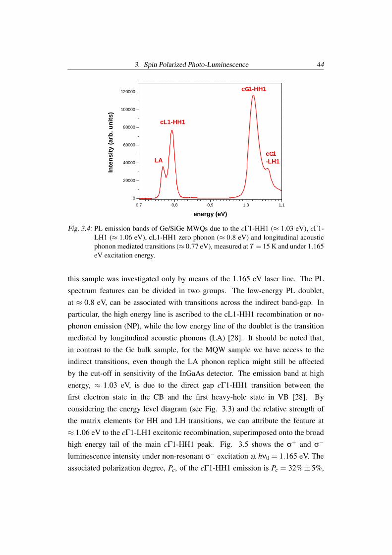
3. Spin Polarized Photo-Luminescence 44
0 , 7 0 , 8 0 , 9 1 , 0 1 , 10
2 0 0 0 0
4 0 0 0 0
6 0 0 0 0
8 0 0 0 0
1 0 0 0 0 0
1 2 0 0 0 0
c G 1- L H 1
c G 1 - H H 1
c L 1 - H H 1
Inten
sity (
arb. u
nits)
e n e r g y ( e V )
L A
Fig. 3.4: PL emission bands of Ge/SiGe MWQs due to the cΓ1-HH1 (≈ 1.03 eV), cΓ1-LH1 (≈ 1.06 eV), cL1-HH1 zero phonon (≈ 0.8 eV) and longitudinal acousticphonon mediated transitions (≈ 0.77 eV), measured at T = 15 K and under 1.165eV excitation energy.
this sample was investigated only by means of the 1.165 eV laser line. The PLspectrum features can be divided in two groups. The low-energy PL doublet,at ≈ 0.8 eV, can be associated with transitions across the indirect band-gap. Inparticular, the high energy line is ascribed to the cL1-HH1 recombination or no-phonon emission (NP), while the low energy line of the doublet is the transitionmediated by longitudinal acoustic phonons (LA) [28]. It should be noted that,in contrast to the Ge bulk sample, for the MQW sample we have access to theindirect transitions, even though the LA phonon replica might still be affectedby the cut-off in sensitivity of the InGaAs detector. The emission band at highenergy, ≈ 1.03 eV, is due to the direct gap cΓ1-HH1 transition between thefirst electron state in the CB and the first heavy-hole state in VB [28]. Byconsidering the energy level diagram (see Fig. 3.3) and the relative strength ofthe matrix elements for HH and LH transitions, we can attribute the feature at≈ 1.06 eV to the cΓ1-LH1 excitonic recombination, superimposed onto the broadhigh energy tail of the main cΓ1-HH1 peak. Fig. 3.5 shows the σ+ and σ−
luminescence intensity under non-resonant σ− excitation at hν0 = 1.165 eV. Theassociated polarization degree, Pc, of the cΓ1-HH1 emission is Pc = 32%± 5%,

3. Spin Polarized Photo-Luminescence 45
well above the maximum theoretical limit of Pc = 25% achievable in bulk Ge.As already mentioned, with a photon energy of 1.165 eV we excite both the cΓ1-HH1 and cΓ1-LH1 transitions. Under this condition and according to calculationsin Ref. 22, the initial spin polarization Ps, right after absorption is expected tobe comprised between Ps = 28−34%, while the subsequent circular polarizationfor light emission at the cΓ1-HH1 transition is about 96% of Ps, finally yieldingan expected polarization degree of the luminescence in agreement with ourexperimental results. Substantially higher values of Pc could be hence achievedfor the limiting case of cΓ1-HH1 resonant- excitation. Such finding demonstratesthe effectiveness of strain and quantum confinement effects for the optical controlof spin injection in SiGe heterostructures. Heteroepitaxial growth of Ge MQWstherefore provides an effective means to engineer optical injection of spins even ingroup IV materials, traditionally considered not suitable for optical studies of spinphenomena. The consistency between our spin resolved PL data and calculationsconcerning electron polarization on Ge/SiGe MQWs of Ref. 22 suggests that afteroptical orientation electron depolarization mechanisms are negligible even fornon-resonant excitation and that heavy holes are equally distributed between theirm j sublevels, i.e. they are completely unpolarized. In particular, the mechanismsleading to the same |3/2,−3/2〉 and |3/2,3/2〉 hole populations take place ona time scale which is faster than the electron spin relaxation time despite thedecrease in the valence band mixing due to confinement effects. Remarkably, inthe cΓ1-LH1 recombination channel, a clear σ− contribution is reported, whileσ+ emission is found to be almost missing. By subtracting the broad highenergy tail of the HH1 transition we can estimate a polarization degree as high as≈ 86%± 8%: this result strongly suggests that LH are still partially polarized atthe moment of electron-hole recombination. After σ− excitation only m j =+1/2light holes are created, and since the weak cΓ1-LH1 −σ+ emission is relatedto ms = +1/2-spin electrons recombining with m j = −1/2 light holes, we mustargue that the latter are not sizably present in the sample. Spin polarized PLmeasurements therefore indicate that photo-generated |3/2,+1/2〉 holes do notloose their spin orientation, but either recombine radiatively with |1/2,−1/2〉electrons, or thermalize their momentum and energy to the HH levels, eventuallyto the |3/2,−3/2〉 states via preserving parity scattering events [73]. In this

3. Spin Polarized Photo-Luminescence 46
0 , 7 0 , 8 0 , 9 1 , 0 1 , 10
2 0 0 0 0
4 0 0 0 0
6 0 0 0 0
8 0 0 0 0
1 0 0 0 0 0
1 2 0 0 0 0
s - s +
Inten
sity (
arb.un
its)
e n e r g y ( e V )Fig. 3.5: Spin Polarized Photo-Luminescence (SPPL) spectra of Ge/SiGe MQWs,
measured at T = 15 K and under 1.165 eV excitation energy having a right-handcircular polarization (σ−). Direct and indirect gap features of the spectrum areresolved for left-hand, σ− (blue), and right-hand σ+ (red) circular polarization.
way LH can indeed contribute to counterbalance the |3/2,3/2〉 hole populationproduced during the absorption. It is noteworthy that due to the aforementionedcooling process towards HH states at lower energy, which is mainly mediated byacoustic phonon scattering, the lifetime of the LH exciton is expected to be shorterthan that of the HH exciton. The different polarization for the cΓ1-LH1 and cΓ1-HH1 excitons suggests that the observed spin polarization is determined by thesingle particle lifetime. Noticeably, in Ge the spin relaxation time of holes, τh
sh, hasto be compared with a mechanism completely absent in III-V compounds, namelyelectron scattering to the side valleys, τe. This phenomenon may have a significantimpact on the spin dynamics, since it reduces the permanence of electrons inthe Γ region to hundreds of fs and therefore limits the exciton lifetimes [73, 74].Experimental data for τh
sh are not yet available even for bulk Ge, but are expectedto be in the 0.1-10 ps range [26,75]. These results suggest that the time needed toequalize the HH population on their m j sublevels is shorter than τe ≈ 500 fs [73],whereas the spin relaxation time for LH is larger or at least comparable with theΓ-electron lifetime.

3. Spin Polarized Photo-Luminescence 47
After direct gap excitation at hν0 = 1.165 eV, the decay of photo-generatedelectrons towards the Γ-valley band edge competes with the Γ-L depopulation,which leads to the NP and phonon replica LA emissions. Noticeably, also suchindirect transitions are polarized, in particular the NP band at≈ 792 meV, recordedfor both σ+ and σ− polarizations reveals a net light polarization degree of about9% and the LA band displays a polarization degree of about 8%. This is aclear indication that the electron-phonon interaction, responsible for L-valleypopulation, and the subsequent momentum-assisted recombination do not leadto a complete lost of the spin orientation. In this case the evaluation of theelectron spin polarization from the measured Pcirc is much more complicated thanin the case of direct transitions, due to the mixed s-p-d nature of the L state [22]and the required momentum transfer. Only very recently such problem has beenaddressed from a theoretical point of view for phonon assisted transitions in bulkSi [23]. Corresponding calculations are not available for Ge, and, in particular, aremissing for the zero-phonon line, which is allowed by small deviations from a noncubic environment associated to interface roughness and strain. The comparisonof experimental circular polarization values with future theoretical studies of zero-phonon optical transitions is therefore mandatory to gather access to the spinphysics of low dimensional structures based on indirect band-gap materials.

Part II
PROBABILITY-CURRENT AND SPIN-CURRENT IN
PRESENCE OF SPIN-ORBIT INTERACTION

49
3.3 Introduction
The following work is focussed on transport phenomena in presence ofSpin- Orbit Interaction (SOI) [76]; evidently semiconductors play a key rolein this matter because in this case it is possible to use an approach, closeto atomic physics, which relies on the exact knowledge of the electron wave-function. In particular III-V semiconductor compounds are paradigmatic systemsto study spin-related transport properties: in fact they do not have bulk inversionasymmetry (Td-symmetry point group) so that the spin degeneracy is removedby the well known D’yakonov-Perel (DP) field, which has a cubic dependenceversus the wave-vector k [77, 78]. Moreover, in 2D heterostructures, a linearRashba field [79, p. 178] arises, due to the structural inversion asymmetry[80, 81]. Basically this means that in such compounds, when low dimensionalheterostructures are taken into account, the two main SOI terms can be studied sothat III-V semiconductor compounds, like GaAs, result really appealing to studyspin-related properties of charge particles.
Evidently the two relevant quantities for transport phenomena are theprobability- current and the spin-current; the probability current is a fundamentalconcept in quantum mechanics, which connects the wave-like description of aquasi-particle to the notion of transport current. When a general Schrödingerproblem is considered, the Hamiltonian is
H0 =p2
2m+U(r) , (3.1)
where the real potential U(r) is periodic in a crystalline solid and m is the free-electron mass; in this case one is led to the usual definition of free-electron currentprobability [82, p. 238]:
J f [ψ] = Re[
ψ∗ p
mψ
]=
~m
Im [ψ∗∇ψ] . (3.2)
However, in condensed-matter systems in the presence of Spin-Orbit Interaction(SOI), the potential is no longer real so that a redefinition of this quantity ismandatory. A debated example of this subtle point is provided by semiconductors-

50
based systems, whose proper treatment requires consideration of the Hamiltonian
H = H0 + HSO (3.3)
withHSO =
~4m2c2 (∇U× p) · σ. (3.4)
Due to the fact that SOI terms in the Hamiltonian have a dependence with respectto the power of the momentum operator p, it is reasonable to express the fullHamiltonian, involving SOI terms, as an effective Hamiltonian which consists ofmomentum-operator p-power series expansion, as already shown by Hoai Nguyenet al. [83]: indeed, beside the kinetic energy, quadratic in p, the SOI providesleading terms that are linear and cubic in p, known respectively as Rashba [79]and D’yakonov-Perel (DP) [77, 78] terms. Then, since the SOI potential is nonreal, a more general definition of the probability current J[ψ] has necessarily to betaken into account. Considering interactions that include higher-order polynomialterms in the Hamiltonian, we have to deal with an effective Hamiltonian of ordern.
Furthermore, an open question, strictly linked to the one above, concerns thedefinition of spin current (SC). Indeed, in semiconductor physics, that providesparadigmatic systems for spintronics, it is known that the SC standard definition,used by many authors [84–89], can be suitably applied to two dimensional(2D) systems with Rashba SOI, but fails to describe spin-dependent transportphenomena in bulk cubic semiconductors, where SOI induces a DP term in theconduction band. The existence of extra-current terms was also pointed out inRef. 90. Drouhin et al. [91] have shown that a redefinition of SC is mandatoryto obtain a unified treatment, enlightening the fact that a properly-symmetrizedspin-current operator J↑(↓)[ψ], where ↑ (↓) refers to up (down) spin channel, givesunexpected results when applied to tunneling through evanescent states in GaAsbarriers.
As pointed out by Rashba in Ref. 85, there are still concerns relying on thefact that a consistent theory of spin transport currents has not been formulated yet.From a general point of view, it means that we cannot immediately approach sucha topic in terms of non equilibrium thermodynamics. In fact, a difficulty relies

51
on the definition of system in order to formulate relevant balance equations andalso on the boundary terms which should possibly be included in the effectiveHamiltonian. Recently, Shi et al. [92] have proposed an alternative spin-currentoperator, satisfying the continuity equation, that allegedly supports importantconclusions concerning conservation of spin currents [93–95], but which appearsto rely on non-explicit assumptions (see Sec. 4).
The inclusion of SOI in the Hamiltonian of a system has direct and practicalconsequences in heterostructures, where a consistent analysis of the tunnelingphenomena is required. The pragmatic BenDaniel-Duke (BDD) approach [96],that perfectly works when dealing with quadratic Hamiltonians under effective-mass approximation, cannot be straightforwardly extended because it is notalways possible to ensure both the continuity of the envelope function and theconservation of the probability current, which is mandatory under steady-stateconditions. Then it is necessary to revisit both the probability-current expressionand the boundary conditions. This is in line with the ideas of Harrison [97].
In this chapter, a systematic construction of the probability-current operator Jis presented, which is based on an effective Hamiltonian written as a p-powerseries expansion. The relation between the velocity operator and the currentoperator, evidencing the simple structure of the extra terms will be analyzedto yield easy and compact calculations whereas explicit treatments in particularcases resulted in lengthy calculations [90]. This novel current operator can besubsequently used to build the SC operators according to the procedure describedin Ref. 91. Then, the proper of an hereostructure interface is studied, in orderto introduce proper matching conditions at the boundaries, which generalizethe BDD procedure, the simplest efficient way to deal with semiconductorheterostructures. Finally, this method is applied on three examples: the case ofa quadratic Hamiltonian, where we recover the usual situation (continuity of theenvelope function and of the velocity), the case where a Rashba term is added asa perturbation to the BDD Hamiltonian (there we find that the envelope functionis continuous, but its derivative is discontinuous), and the case where a cubic DPterm is added to the BDD Hamiltonian (where we prove that the envelope functioncannot be continuous).
The layout of the chapter is as follows: Sec. 4 is devoted to a general

52
construction of current operators and a derivation of local properties. In Sec.5, a general Hamiltonian H(n) is introduced as nth-degree homogenous functionof momentum-operator coordinates with the subsequent derivation of the velocityoperator; moreover it is shown that a proper symmetrization yields the Hermitiancurrent operator J. Sec. 5.4, boundary conditions which are suitable to dealwith heterostructures, are proposed and in Sec. 5.5, they are applied to electrontunneling through a [110]-oriented GaAs barrier. Finally, in Sec. 5.6, the problemof the spin-current definition will be taken into accout in order to show howto extend the construction procedure to the spin current operators. For furtherinformation the reader can refer to Ref. 76, 98.

4. GENERAL DEFINITION OF CURRENT OPERATORS
A difficulty, that arises when a current operator is taken into account, relies onthe correct definition of the system and of its boundaries: in fact, considering thedensity ρ of a physical quantity, we need to satisfy the continuity equation of J,defining a source term G, so that:
∂ρ
∂t+∇ ·J = G. (4.1)
As pointed out in Ref. 92, the continuity of J can be ensured by introducing ageneral source term G, as in Eq. 4.1, but the source term is not uniquely definedand this leads to possible confusion when considering the conservation laws interms of non-equilibrium thermodynamic equations. In fact, a thermodynamicmodel only based on the continuity equation Eq. 4.1 cannot take into account theexchange of energy e with the environment introduced by the current generatorand the spin-orbit interaction. Indeed, the consequence of the Gibbs equation
dedt
= T∂s∂t
+µ∂ρ
∂t(4.2)
where s is the entropy, T the temperature, and µ is the chemical potential, isthat the continuity equation of the density of carriers ρ is necessarily determinedby the power dissipated at the boundaries. At zero temperature, the sourceterm is equal to the power dissipated divided by the chemical potential ∂ρ/∂t =
(1/µ)de/dt. This is the reason why the decomposition between the divergenceterm and the source term G cannot be unique without specifying the boundaryconditions. In any case, we first need to state clearly the local properties ofa current operator, postponing the analysis of its global properties. For thispurpose, we consider a linear operator A that does not explicitly depend on

4. General definition of current operators 54
time and acts over a generic state ψ. In the following we adopt the notation(A)=(
ψ
∣∣∣Aψ
)= ψ†Aψ used in Ref. 83. The general Schrödinger problem
reads:i~
∂
∂tψ = H ψ (4.3)
where H may be any Hamiltonian. For example H may be equal to H (definedin Eq. 3.3) or to He f f (defined below in Eq. 5.1). We explicitly develop thederivative of A with respect to time:
∂
∂t
(A)=
∂
∂t
(ψ
†Aψ
)=
∂
∂t
(ψ
†)
Aψ+ψ†A(
∂
∂tψ
)(4.4)
and with the help of Eq. 4.3 we obtain:
∂
∂t
(A)=− 1
i~
(H ψ
)†Aψ+
1i~
ψ†A(
H ψ
)=
1i~
[ψ
† AH ψ−(
H ψ
)†Aψ
].
(4.5)If A is an Hermitian matrix (the elements of which are complex numbers, notdifferential operators) (
H ψ
)†Aψ =
(ψ
† AH ψ
)∗, (4.6)
so that we can rewrite Eq. 4.5 in a more suitable way that we refer to as the localform of Ehrenfest theorem:
∂
∂t
(A)=
2~
Im(
ψ† AH ψ
). (4.7)
The integration over the whole space leads to the well known Ehrenfest’s theorem,whose global form is valid for any (possibly differential) Hermitian operator A:
∂
∂t
⟨A⟩=
1i~
[⟨ψ
∣∣∣AH∣∣∣ψ⟩−⟨H ψ
∣∣∣A∣∣∣ψ⟩]= 1i~
⟨ψ
∣∣∣[A,H ]∣∣∣ψ⟩ . (4.8)
We can write
∂
∂t
(A)=
1~
Im(
ψ†{
A,H}
ψ
)+
1~
Im(
ψ†[A,H
]ψ
)(4.9)

4. General definition of current operators 55
with{
a, b}= a b+ b a, and, by integration over the whole space, we get
∫d3rIm
(ψ
†{
A,H}
ψ
)= 0. (4.10)
The time derivative of(
A)
is composed of two parts, concerning two differentphysical processes: we respectively recognize in Eq. 4.9 the divergence of thecurrent and the source term G associated to A
∇ ·JA =− 1~
Im(
ψ†{
A,H}
ψ
)=− 1
~Im(
ψ†{
A,H −U}
ψ
), (4.11)
where any real potential U vanishes when taking the imaginary part of theanticommutator, and
G =1~
Im(
ψ†[A,H
]ψ
). (4.12)
The above procedure has two advantages: first, we have expressed in ageneral form all the quantities entering Eq. 4.1 through commutators andanticommutators; then we have related the probability-current expression directlyto the local properties of its corresponding operator, without taking into account aclosed system (such a procedure does not automatically imply that the integral of∇ ·JA over the crystal only is zero). The choice of considering open systems makesthe current operator involve Dirac distributions to deal properly with possiblediscontinuities at the boundaries of a subsystem. It has to be noted that it is alwayspossible to include the source G term in the form of a current JG, G = ∇ ·JG sothat the conservation equation becomes
∂
∂t
(A)+∇ · (JA−JG) =
∂
∂t
(A)+∇ ·J=0 (4.13)
where J = JA − JG is divergence-free in steady-state regime. For instance, ifwe look for JG = ∇UG, the potential UG is a solution of the Laplacian problem∆UG = G. Moreover, adding to JG the term ∇×AG, where AG is an arbitraryvector field, does not affect the conservation equation. At this stage, the boundaryconditions are not under control. In Ref. 92 the authors observe that it might often

4. General definition of current operators 56
happen that ∫V
d3r G = 0 (4.14)
where the integration is performed over the volume of the system (V). Then∫V
d3r G =∫V
d3r ∇ ·JG =∫S
JG ·ds = 0 (4.15)
where the volume integral is changed into a surface integral through Ostrograd-ski’s theorem (here S is the surface limiting V and ds is the surface elementalong the normal to S). Such a relation is obviously satisfied provided thatJG ·ds = 0, i.e., provided that JG is a tangential vector to S, which is “physically”reasonable. Moreover one can further assume, as reported in Ref. 92 that JG “is amaterial property that should vanish outside the sample”: this is a more restrictiveand questionable hypothesis. For instance in the case of a magnetic field, theeffect of the associated vector potential cannot a priori be overlooked outside thesample. Anyway, let us assume that JG = 0 at the surface S. In this case it isstraightforward to show, after partial integration where the boundary contributioncancels, that ∫
dy dz dx x(
∂JG,x
∂x+
∂JG,y
∂y+
∂JG,z
∂z
)=−
∫d3r JG,x (4.16)
where JG,x, JG,y, and JG,z are the Cartesian components of JG. Then∫d3r JG =−
∫d3r r∇ ·JG =−
∫d3r rG
=−1~
∫d3r r Im
(ψ
†[A,H
]ψ
)=−1
~
∫d3r Im
(ψ
†r[A,H
]ψ
).
(4.17)
It is easy to check that, provided that[A,r]= 0,
r[A,H
]=[Ar,H
]− i~vA, (4.18)

4. General definition of current operators 57
where[r,H
]= i~v. Thus
∫d3r JG =−1
~
∫d3r Im
(ψ
†[Ar,H
]ψ
)+
∫d3r Re
(ψ
†vAψ
)=−1
~
∫d3r Im
(ψ
†[Ar,H
]ψ
)+
∫d3r JA. (4.19)
Here, JA is the canonical current defined as
JA = Re(
ψ† v Aψ
)= ψ
† v A+ A v2
ψ. (4.20)
According to Eq. 4.5, we can write
∫d3r JG =−
∫d3r
d(
Ar)
dt−JA
=∫
d3r
JA−d(
Ar)
dt
. (4.21)
In Ref. 92 the effective current density is defined as JG
JG = JA−d(
Ar)
dt.
We have the two following relations which define respectively the total current Jand the effective total current J
J = JA−JG, (4.22a)
J = JA−JG =d(
Ar)
dt+(
JA− JA
). (4.22b)
Provided JA− JA = 0, i.e. when making the confusion between the canonical andthe true currents (which is justified only for Hamiltonians up to second order in p,see Sec. 5), the effective total current becomes J =d
(Ar)/dt, which is Eq. 5 in
the papers by Shi et al. [92] and also by Zhang et al., [94] and is the cornerstoneof their further calculations. After a careful analysis, this relation appears to bederived under very special conditions so that it cannot be general. Moreover, themeaning of the so-called effective currents and their relationship with the true
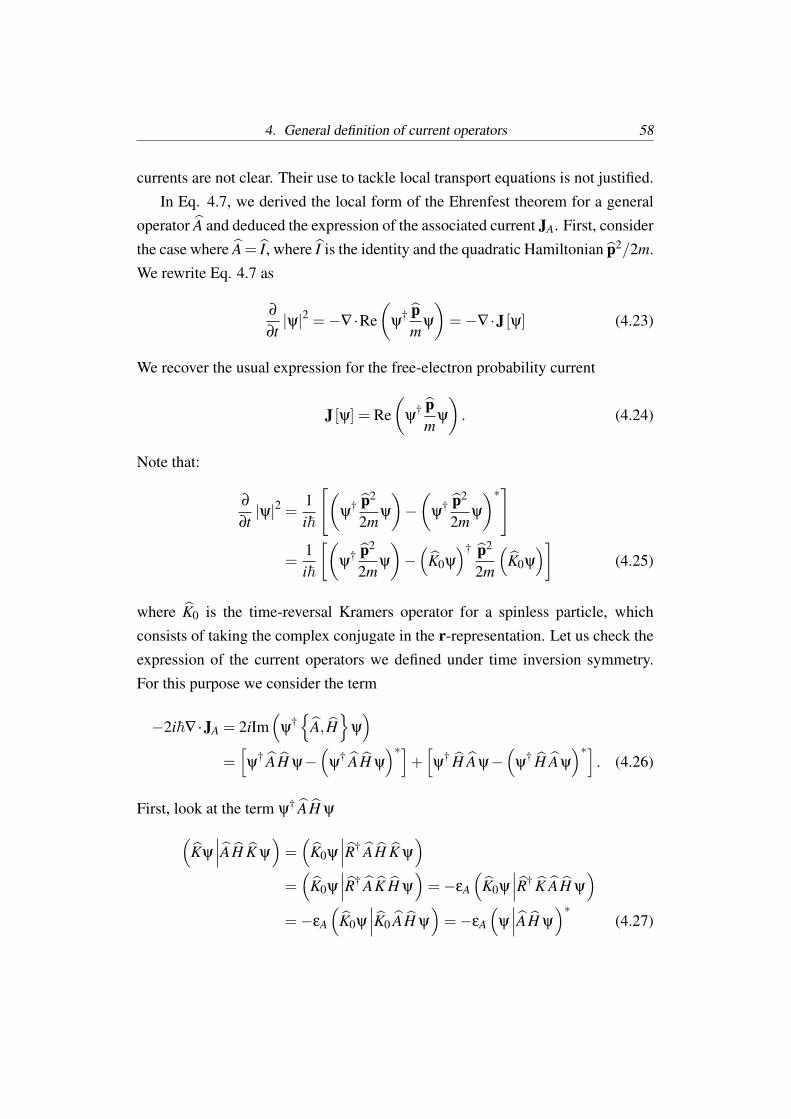
4. General definition of current operators 58
currents are not clear. Their use to tackle local transport equations is not justified.In Eq. 4.7, we derived the local form of the Ehrenfest theorem for a general
operator A and deduced the expression of the associated current JA. First, considerthe case where A= I, where I is the identity and the quadratic Hamiltonian p2/2m.We rewrite Eq. 4.7 as
∂
∂t|ψ|2 =−∇ ·Re
(ψ
† pm
ψ
)=−∇ ·J [ψ] (4.23)
We recover the usual expression for the free-electron probability current
J [ψ] = Re(
ψ† p
mψ
). (4.24)
Note that:
∂
∂t|ψ|2 = 1
i~
[(ψ
† p2
2mψ
)−(
ψ† p2
2mψ
)∗]
=1i~
[(ψ
† p2
2mψ
)−(
K0ψ
)† p2
2m
(K0ψ
)](4.25)
where K0 is the time-reversal Kramers operator for a spinless particle, whichconsists of taking the complex conjugate in the r-representation. Let us check theexpression of the current operators we defined under time inversion symmetry.For this purpose we consider the term
−2i~∇ ·JA = 2iIm(
ψ†{
A, H}
ψ
)=[ψ
† A H ψ−(
ψ† A H ψ
)∗]+[ψ
† H Aψ−(
ψ† H Aψ
)∗]. (4.26)
First, look at the term ψ† A H ψ(Kψ
∣∣∣A H K ψ
)=(
K0ψ
∣∣∣R† A H K ψ
)=(
K0ψ
∣∣∣R† A K H ψ
)=−εA
(K0ψ
∣∣∣R† K A H ψ
)=−εA
(K0ψ
∣∣∣K0 A H ψ
)=−εA
(ψ
∣∣∣A H ψ
)∗(4.27)

4. General definition of current operators 59
Here, K = R K0 is the Kramers operator for a particle with spin 1/2, R = −iσy(R† = R−1
), and εA =±1 depending wether A verifies [99, p. 675]
K A K = εA A or R† A R = εA A∗. (4.28)
Similarly, for the term ψ† H Aψ(Kψ
∣∣∣H A K ψ
)=−εA
(K0ψ
∣∣∣R† K H Aψ
)=−εA
(K0ψ
∣∣∣K0 H Aψ
)=−εA
(ψ
∣∣∣H Aψ
)∗. (4.29)
Thus, we obtain
2iIm(
ψ†{
A, H}
ψ
)= ψ
†{
A, H}
ψ+ εA
(Kψ
)†{A, H
}(Kψ
). (4.30)
We conclude that the general expression for the current of A is
∇ ·JA =− 12i~
[ψ
†{
A, H}
ψ+ εA
(Kψ
)†{A, H
}(Kψ
)]. (4.31)
5. PROBABILITY CURRENT OF AN EFFECTIVE
HAMILTONIAN
5.1 Formulation of the general nth-order Hamiltonian
Considering effective Hamiltonians, we deal with general expressions givenby momentum series expansions, i.e., constructed from the energy expressed aswave-vector-component series expansion after the substitution {k −→−i∇}. Wewrite the effective Hamiltonian He f f as follows:
He f f = Hp +V (r) (5.1)
where V (r) is a potential which may be the potential of a single barrier or the oneof a superlattice, for example, Hp is such that
Hp = ∑n
∑l(k)∈{x,y,z}k=1,...,n
cl(1),l(2),...,l(n) pl(1)...pl(n) = ∑n
H(n) (5.2)
where pl(k) is the momentum operator associated to the l(k) Cartesian coordinateand where cl(1), ...,l(n) are Hermitian matrices which are invariant under permu-tation of the subscripts. The abstract form of Eq. 5.2 allows us to perform easycalculations. In Sec. 5.2 we show how to handle such a general expression to dealwith concrete situations.
Formally, we perform the identification
cx...cx︸ ︷︷ ︸α
cy...cy︸ ︷︷ ︸β
cz...cz︸ ︷︷ ︸γ
= cx...x︸︷︷︸α
, y...y︸︷︷︸β
, z...z︸︷︷︸γ
(5.3)

5. Probability current of an effective Hamiltonian 61
where α, β, and γ are integers. We obtain
H(n) = (cx px + cy py + cz pz)n . (5.4)
Given Eqs. 5.2, 5.3, and 5.4, let us note that only terms such as cxx or cxy (forn = 2) are meaningful, a term such as cx being only a trick in the calculation.
Alternatively, one can write
H(n) = ∑α+β+γ=n
cαβγ pαx pβ
y pγz (5.5)
withcαβγ =
n!α!β!γ!
cαx cβ
y cγz (5.6)
We are now in a position to tackle the problem of velocity, first when theHamiltonian H takes into account the SOI, and, second, when the HamiltonianHe f f is an effective Hamiltonian.
5.2 Velocity operator in presence of SOI interaction
It is usually admitted that the velocity operator v is equal to ∂H /∂p whateverthe Hamiltonian H . However, to the best of our knowledge, the derivation can befound only when H is quadratic in p. Therefore a general derivation, in particularin the case of effective Hamiltonians, is mandatory. We start from Ehrenfest’stheorem (valid whatever the Hamiltonian H )
〈v〉= d〈r〉dt
=i~
⟨[H , r
]⟩(5.7)
If (i/~)⟨[
H , r]⟩
=⟨
∂H /∂p⟩
, then v = ∂H /∂p because two linear operators
which have the same mean values over all possible states are equal:⟨
A⟩=⟨
B⟩
implies that A = B [99, p. 633] Practically, it is enough to show that
(i/~)[H , r
]= ∂H /∂p to prove that v = ∂H /∂p.
First, considering the case H = H0 which contains a H(2) term (Eq. 3.1),
5. Probability current of an effective Hamiltonian 62
(i/~)[H0, r
]= (~/im) p= ∂H0/∂p, for a system described by an Hamiltonian
quadratic versus momentum components, and we obtain the velocity v0:
v0 =∂H0
∂p. (5.8)
Second, we have to check that this relation still holds in the presence of SOI wherethe Hamiltonian is H = H = H0+ HSO (Eq. 3.3). In other words we want to showthat
v =∂H∂p
. (5.9)
We know that v0 = (i/~)[H0, r
]= ∂H0/∂p. To show that Eq. 5.9 is valid, it is
enough to show that vSO = ∂HSO/∂p, which will give v= ∂H/∂p with v= v0 +
vSO. A straightforward calculation yields
vSO =i~[HSO, r] =
~4m2c2 (σ×∇U) =
∂HSO
∂p(5.10)
which proves Eq. 5.9: the derivative of the Hamiltonian, with respect to themomentum operator, still provides a suitable definition of the velocity when theSOI term is taken into account.
5.3 Velocity operator with an effective Hamiltonian He f f
We generalize the results obtained in Sec. 5.2, to the case of a generic effectiveHamiltonian H = He f f . Again we exploit Ehrenfest’s theorem, as written in Eq.5.7. Considering for instance the x component, we verify that
[H(n), x
]= ∑
α+β+γ=ncαβγ
(~i
)α pα−1
x pβy pγ
z =~i
∂H(n)
∂ px(5.11)
ori~
[Hp, r
]=
i~
[Heff, r
]=
∂He f f
∂p(5.12)

5. Probability current of an effective Hamiltonian 63
which proves that
v =∂He f f
∂p. (5.13)
Using Eqs. 5.3-5.6, it is then easy to calculate the j component v(n)j ( j = x, y, z)
of the velocity operator v(n) associated to H(n):
v(n)j =∂H(n)
∂ p j= nc j (cx px + cy py + cz pz)
n−1 . (5.14)
We introduce the scalar product between the momentum p and the velocityoperator v(n)
pxv(n)x + pyv(n)y + pzv(n)z = n(cx px + cy py + cz pz)
n = nH(n). (5.15)
With this notation, v0, introduced in the paragraph 5.2, is such that v0 = v(2). Eq.5.15 means that
p · v(n) = nH(n) (5.16)
and eventually
He f f ψ =
(p · ∑
n
1n
v(n))
ψ+V ψ = Eψ. (5.17)
As pointed out in Sec. 4, we are allowed to define current operatorsin open systems provided that we properly take into account their boundaryconditions. We are interested in finding the form of the current operatorJ =
(Jx, Jy, Jz
)for an Hamiltonian H(n) +V (r) - the current operator being
J(n) - and more generally for the Hamiltonian He f f = Hp +V (r) = ∑n H(n) +
V (r) (Eqs. 5.1-5.2) - the current operator being J. For an Hamiltonianp2/2m + V (r), it is known [99, p. 372] that the jth component of thecurrent operator ( j = x, y, or z) at the point r0 is of the shape J(2)j (r0) =
(1/2m)[δr0 p j + p j δr0
], where δr0 is the Dirac distribution, centered in r = r0;
with the notation of Eqs. 5.1-5.2, H(2) = ∑l(k)∈{x,y,z}k=1,2
cl(1),l(2) pl(1) pl(2), J(2)j (r0) =
∑l(1)={x,y,z} c j,l(1)[δr0 pl(1)+ pl(1) δr0
], cl(1),l(2) = (1/2m)δl(1),l(2). The aim of
the following procedure is to show that, for an Hamiltonian H(n) +V (r), the

5. Probability current of an effective Hamiltonian 64
following form of the jth component of the probability current operator
J(n)j (r0) = ∑l(k)∈{x,y,z}
k=1,..,n−1
c j,l(1),...,l(n−1)[δr0 pl(1) pl(2)...pl(n−1)
+pl(1)δr0 pl(2)...pl(n−1)+ ...+ pl(1) pl(2)...pl(n−1)δr0
](5.18)
gives back Eq. 4.11, where δr0 = δ(r− r0) is again the Dirac distribution, whichinteracts with the mixed powers of the current operator so that the symmetrizationprocedure used in the construction of J(n)j (r0) provides (n−2) further summations
with respect to J(2)j (r0). The two definitions coincide only up to n = 2. The extraterms are crucial in order to satisfy the continuity equation. We evaluate everyterm over a generic state ψ; for example the second term is of the shape
⟨ψ∣∣pl(1)δr0 pl(2)...pl(n−1)
∣∣ψ⟩= ∫d3r ψ
∗ pl(1)δr0 pl(2)...pl(n−1)ψ
=∫
d3r(
pl(1)ψ)†
δr0 pl(2)...pl(n−1)ψ
=[pl(1)ψ(r0)
]† pl(2)...pl(n−1)ψ(r0) . (5.19)
Then the jth Cartesian component of probability current for a generic state J j [ψ]
can be written as:
J(n)j [ψ] =⟨
ψ
∣∣∣J(n)j (r0)∣∣∣ψ⟩= ∑c j,l(1),...,l(n)
l(k)∈{x,y,z}k=1,..,n−1
[ψ
† pl(1)...pl(n−1)ψ+ ...
+(
pl(1)...pl(k−1)ψ)† pl(k)...pl(n−1)ψ+ ...+
(pl(1)...pl(n−1)ψ
)†ψ
](5.20)
where ψ = ψ(r0). From Eq. 5.20, we can find the generic divergence term related

5. Probability current of an effective Hamiltonian 65
to the derivative with respect to p j:
p jJ(n)j [ψ] = ∑
l(k)∈{x,y,z}k=1,..n−1
c j,l(1),...,l(n)
[ψ
† p j pl(1)...pl(n−1)ψ−(
p jψ)† pl(1)...pl(n−1)ψ
+(
pl(1)...pl(k−1)ψ)† p j pl(k)...pl(n−1)ψ−
(p j pl(1)...pl(k−1)ψ
)† pl(k)...pl(n−1)ψ
+(
pl(1)...pl(k)ψ)† p j pl(k+1)..pl(n−1)ψ−
(p j pl(1)...pl(k)ψ
)† pl(k+1)...pl(n−1)ψ
+...+(
pl(1)...pl(n−1)ψ)† p jψ−
(p j pl(1)...pl(n−1)ψ
)†ψ
]. (5.21)
In Eq. 5.21 all the terms that have the same order in k (two consecutive terms butthe first one and the last one) vanish after summation over j:
∑j={x,y,z}
∑l(k)∈{x,y,z}k=1,..n−1
c j,l(1),...,cl(n)
[−(
p j pl(1)...pl(k−1)ψ)† pl(k)...pl(n−1)ψ
+(
pl(1)...pl(k)ψ)† p j pl(k+1)..pl(n−1)ψ
]= 0 (5.22)
Then the only terms still remaining in the summation are:
∑j={x,y,z}
p jJ(n)j [ψ] = p ·J(n) [ψ]
= ∑j={x,y,z}
∑l(k)∈{x,y,z}
k=1,..,n−1
c j,l(1),...,cl(n)
[ψ
† p j pl(1)...pl(n−1)ψ−(
p j pl(1)...pl(n−1)ψ)†
ψ
]= ∑
j={x,y,z}∑
l(k)∈{x,y,z}k=1,..,n−1
2i c j,l(1),...,cl(n)Imψ† p j pl(1)...pl(n−1)ψ. (5.23)
Now ∇ ·J(n) [ψ] = (i/~) p ·J(n) [ψ] and Eq. 5.24 results in a collection of pureimaginary terms and the final expression for the divergence of the probabilitycurrent reads:
∇ ·J(n) [ψ] =−2~
Im ∑j={x,y,z}
∑l(k)∈{x,y,z}
k=1,..,n−1
c j,l(1),...,l(n)(ψ∣∣p j pl(1)...pl(n−1)
∣∣ψ) .
(5.24)

5. Probability current of an effective Hamiltonian 66
Eventually∇ ·J [ψ] = ∑
n∇ ·J(n) [ψ] .
Thus we have shown that the hermitian symmetrized probability-current operatorof Eq. 5.18 satisfies the continuity equation for the effective Hamiltonian of Eq.5.1.
Obviously, adding a term proportional to the curl of any vector field wouldnot affect the result. Such a definition of J provides an unambiguous and generaltool for evaluating the probability current. Provided the Hamiltonian of the wholesystem is known, this probability-current operator guarantees the requirements ofthe continuity equation.
Now it is useful to introduce the Hermitian symmetrized velocity operator
v(n)j (r0) =
n2 ∑
l(k)∈{x,y,z}k=1,..,n−1
c j,l(1),...,l(n−1)[δr0 pl(1)...pl(n−1)+ pl(1)...pl(n−1)δr0
](5.25)
For example for n≥ 2, the comparison between Eqs. 5.18 and 5.25 clearly showsthat J (n)
j (r0) contains n−2 extra terms, which are straightforwardly obtained from∂He f f /∂p. For instance, with He f f ≡ pn, we have ∂He f f /∂p≡ npn−1, so that:
v(n)(r0)≡ (n/2)(δr0 pn−1 + pn−1
δr0
), (5.26)
whereasJ (n) (r0)≡
(δr0 pn−1 + pδr0 pn−2 + ...+ pn−1
δr0
). (5.27)
As shown in Ref. 83, extra terms are specially important for evanescent waves.Therefore, in the following we deal with tunneling problems.
5.4 BenDaniel-Duke-like formulation and boundary conditions
We stress that the central question when defining the current operators andrelated quantities is the proper definition of the system and of its boundaries.Dealing with heterojunctions, where each bulk medium is described by therelevant Hamiltonian, requires defining proper matching conditions at the

5. Probability current of an effective Hamiltonian 67
boundaries. In this sense, the BDD Hamiltonian [96] is the simplest smartapproach that allows solution of the Schrödinger equation over the whole spacewhile it guaranties the conservation of the probability current at the interface. Theprinciple is the following. Let us consider a one-dimensional problem and twodifferent media for x < 0 and x > 0. Each medium is characterized by its ownHamiltonian. The question is to find a solution of the Schrödinger equation, madeof eigenfunctions of the relevant band of the two bulk materials, which ensuresthe continuity of the probability current at the origin. In this sense, the problemis analogous to a scattering problem, where the wave functions are determinedonly at some distance of the scattering potential. Proper matching conditionsrelevant to the extension of the bulk envelope functions at the origin will allowone to determine the envelope function over the whole space. For that, BBDpropose writing an Hamiltonian over the whole space as px [1/2m(x)] px +V (x)
where m(x) is the effective mass in each medium. The integration of this BDDHamiltonian around the boundary automatically ensures the continuity of theprobability current of Eq. 3.2, provided that ψ(x) and [1/m(x)] [∂ψ/∂x] arecontinuous.
Now, consider two regions (1) and (2) and assume that each region is madeof a given crystalline material. We look for the envelope function, solution ofthe Schrödinger equation, which is made from plane waves which are eigenstatesof the crystal, inside each material. Observe that, near the interface, the crystalperiodicity is broken so that the true Hamiltonian and the true eigenfunctions willbecome involved. The principle is then to define proper matching conditionsapplying to the prolongation of the envelope function at the origin. For thatpurpose, we consider a volume V, limited by a surface S, that surrounds aninterface portion. Similarly to the BDD technique, we start from Eq. 5.17 andwe integrate the Schrödinger equation over V. Using Ostrogradski’s theorem,when V tends to zero, we obtain
limV−→0
∫S
(∑n
1n
v(n)ψ)
·ds = 0 (5.28)
where ds is normal to the surface S.

5. Probability current of an effective Hamiltonian 68
For a one dimensional case with the interface at the origin, Eq. 5.28 becomes:
limε→0
[∑n
1n
v(n)ψ]+ε
−ε
= 0 (5.29)
Let us again emphasize that no information is obtained on the true wavefunction near the origin. Eq. 5.29 does not ensure either the continuity of theenvelope function or the existence of derivatives at the interface.
As an illustration, let us consider the case of a Rashba Hamiltonian
He f f = ap+bp2 (5.30)
where a and b are two Hermitian matrices. According to Eq. 5.29, we can writedown the first continuity condition as follows:
[aψ+bpψ]+ε
−ε= 0. (5.31)
Using this condition to solve the problem, and adding a priori the continuityof the envelope function at the interface as a second condition, we verify that theprobability current is indeed continuous at the interface:
J [ψ] = 〈ψ | a+bp | ψ〉+ c.c. (5.32)
Then, the jump of the derivative of the wave function at the interface isdetermined by
[bpψ]+ε
−ε=− [a]+ε
−εψ(0). (5.33)
It is clear then that the BDD approach, introduced to solve a problem witha quadratic Hamiltonian, is also suitable to obtain a solution when a Rashbacontribution is added; then we can say that up to the second order in themomentum-power series expansion of the Hamiltonian, the continuity of a“generalized velocity” (see Eq. 5.29) and the continuity of the wave functionat the interface imply the conservation of the probability current at this point.Remarkably, the boundary conditions that we need to solve the problem drasticallychange when moving to the case of a DP Hamiltonian with cubic terms. The

5. Probability current of an effective Hamiltonian 69
crucial point, that we address in the following, is that we cannot make anyhypothesis about the continuity of the wave function because, if we need to ensureprobability-current conservation at an interface, we must accept an envelopefunction ψ which is no longer continuous.
To give an insight into the expression of the current operator and into theconservation of the probability current, let us again come back to an interfacebetween two semi-infinite one-dimensional media (1) and (2). In each bulkcrystal, the relevant Hamiltonian is
Hr = ∑n
H(n)r +Vr (5.34)
withH(n)
r = γ(n)r pn (5.35)
with r = 1 or r = 2 depending on wether x < 0 or x > 0. Hr admits theeigenfunctions ϕr, associated to the fixed energy E which verify
Hrϕr = Eϕr. (5.36)
We consider the Hamiltonian extended over the whole space as
H= Θ(−x) H1 +Θ(x) H2 (5.37)
where Θ(x) is the Heaviside function.However, strictly speaking, near the heterojunction the spatial periodicity is
broken, so that over a few Wigner-Seitz cells, the true Hamiltonian differs (itpossibly includes interface terms) and the electron states are no longer pure Blochstates. We consider two coordinates, −w1 and w2, so that, in the bulk regions]−∞,−w1] and [w2,+∞[ the electronic structure remains unaffected. Very closeto the heterojunction, the eigenfunctions are not assumed to be explicitly known.We consider a wave function ψ which is an eigenstate of the Hamiltonian overthe whole space at energy E. We expect that, over the domain ]−∞,−w1] ∪[w2,+∞[, ψ coincides with Ψ = Θ(−x−w1)ϕ1 +Θ(x−w2)ϕ2 (we assume that

5. Probability current of an effective Hamiltonian 70
the matching is sufficiently regular). Thus, we have⟨Ψ
∣∣∣H∣∣∣ψ⟩= E[〈ϕ1 | ϕ1〉(1)+ 〈ϕ2 | ϕ2〉(2)
](5.38)
where 〈|〉(r) means summation over the bulk part of region (r). Because thetotal probability in the domain ]−∞,−w1] ∪ [w2,+∞[ has to be conserved, fromEhrenfest’s theorem [Eq. 4.8 with A = Θ(−x−w1)+Θ(x−w2)] we must have
〈ψ |[Θ(−x−w1)+Θ(x−w2) ,H]|ψ〉=⟨
ψ
∣∣∣H∣∣∣Ψ⟩−⟨Ψ
∣∣∣H∣∣∣ψ⟩= 0, (5.39)
i. e., ⟨Ψ
∣∣∣H∣∣∣ψ⟩=⟨
ψ
∣∣∣H∣∣∣Ψ⟩= E 〈ψ |Ψ〉 . (5.40)
Observe that:
H(n)1 [Θ(−x−w1)ϕ1] = γ
(n)1 pn
Θ(−x−w1)ϕ1
= Θ(−x−w1)γ(n)1 pn
ϕ1
+ i~γ(n)1[δ(x+w1) pn−1 + pδ(x+w1) pn−2+
+...+ pn−1δ(x+w1)
]ϕ1
= Θ(−x−w1)γ(n)1 pn
ϕ1 + i~J(n)1 (−w1)ϕ1 (5.41)
So thatH1 [Θ(−x−w1)ϕ1] = EΘ(−x−w1)ϕ1 + i~J1 (−w1)ϕ1 (5.42)
and similarly
H2 [Θ(x+w2)ϕ2] = EΘ(x−w2)ϕ2− i~J2 (w2)ϕ2. (5.43)
EventuallyHΨ = EΨ+ i~
[J1 (−w1)ϕ1− J2 (w2)ϕ2
](5.44)
Then, Eq. 5.40 is satisfied provided that
J2 [ϕ2 (w2)] = J1 [ϕ1 (−w1)] . (5.45)

5. Probability current of an effective Hamiltonian 71
The important point is not the conservation relation, which might appear asphysically obvious, but that, in Eqs. 5.41 and 5.43, the symmetrized currentoperator is automatically generated in the form derived in Eq. 5.18, providinga physical insight into this mathematical expression. Because we only deal withwave functions at some distance from the heterojunction, the continuity of thetrue wave function at x = 0 does not implies the continuity of the envelopefunction Ψ which may be discontinuous. This is in line with the considerations ofHarrison [97]. Eq. 5.29 and 5.45 generate a set of boundary conditions relevantto the tunneling problem.
5.5 The [110]-oriented GaAs barrier
We analyze the case of electron tunneling under normal incidence througha [110]-oriented GaAs barrier, which was shown to be non trivial and solved inspecial cases in Ref. 83. The importance of this particular tunneling configurationcan be well explained by the following argument: if we consider the Γ6c
conduction band of a non-centrosymmetric III-V semiconductor compound, likeGaAs, in the small k approximation, we can give an analytical expression ofthe level splitting due to the Dresselhaus term [100], which has a k3 dependenceversus wave-vector:
E± =~
2m∗(k2
x + k2y + k2
z)+ γ
√k2
x(k2
y − k2z)2
+ k2y(k2
z − k2x)2
+ k2z(k2
x − k2y)2
(5.46)where γ is the strength of the effective D’yakonov-Perel magnetic field [77, 78],which removes the spin degeneracy. Indeed it is straightforward to see that alongthe [110]-direction the spin-splitting is maximum so that this crystallographicaxes is really useful to study the effects of SOI term in GaAs. Concerning withtunneling heterojunctions, we are interested in evanescent waves in the [110]-oriented GaAs barrier. At this purpose, looking at the Hamiltonian of Eq. 5.46,it is possible to see that the k3-dependence of the DP field does not allow pureimaginary tunneling wave-vector so that, in order to deal with real energy lines,we have to take into account the complex wave vector k = 1√
2(Q± iK) [110]
[83]. For complete treatment of evanescent states in non-centrosymmetric III-V

5. Probability current of an effective Hamiltonian 72
semiconductors, the reader is invited to refer to Ref. 101.Hereafter, we apply the tools and boundary conditions presented in this paper
to solve it in a more simple and general manner. We confirm and generalizethe results derived in Ref. 83. In particular, we are able to solve the problemof an heterojunction between a free-electron media and a semiconductor withoutinversion center, where the DP field is a step function, which remained puzzling.In the [110] direction, the one dimensional DP Hamiltonian is:
HDP =γc
~2 p2± γ
2~3 p3 (5.47)
where + (−) refers to the up (down)- spin channel quantized along the DP fielddirection. We consider as solution a general wavefunction written as follows:
ψ = α
(ψ0 +
iβ~γck2 γc pψ0
)eiχz (5.48)
where ψ0 is the zeroth order function that is a solution of the tunneling problemwith energy E and with the potential V when SOI is turned off. Here γck2 =E−V ,α and β are complex parameters to be determined, and χ is a real (see below)wavevector component which is added to k when SOI is turned on. We have therelations
pψ = α
(pψ0 + i
β
~γck2 γc p2ψ0
)eiχz +~χψ, (5.49)
p2ψ = ~2
(E−V
γc−χ
2)
ψ+2~χpψ. (5.50)
We calculate the velocity operators from Eq. 5.14
12
v(2)+13
v(3) =γc
~2 p± γ
2~3 p2 (5.51)
and, according to Eq. 5.29, we find the matching condition[γc
(1± γ
γcχ
)pψ
]+ε
−ε
=∓[
12
γ~(
E−Vγc−χ
2)
ψ
]+ε
−ε
(5.52)
which is a generalization of Eq. (3.50) of Ref. 83.

5. Probability current of an effective Hamiltonian 73
Now, we have to satisfy the conservation of the probability current
J[ψ] =γc
~2
(1± γ
γcχ
)[ψ∗ pψ+ψ(pψ)∗
]± γ
~
(E−V
γc−χ
2)|ψ|2± γ
2~3 |pψ|2 .
(5.53)We obtain here an important result: The envelope function cannot be
continuous at the interface. Indeed, assume ψ to be continuous. Then,after Eq. 5.52, we see that the last term in Eq. 5.53, that we rewrite as±(1/2~3)(γ/γ2
c)
γ2c |pψ|2 must be continuous. This is not possible since γc pψ0
is continuous (unless γ/γ2c is almost continuous, which would be fortuitous).
We have to determine ψ complying the boundary conditions, which is notsimple because the expression providing the current is not a linear function ofψ. However, if we consider γ as a first-order quantity and look for a solutionto first order only, the result is surprisingly simple, as shown below. From theSchrödinger equation - Eq. 5.47 -, we find that χ verifies
γc(2kχ+χ
2)± γ
2(k3 +3k2
χ+3kχ2 +χ
3)= 0 (5.54)
thenχ'∓1
4γ
γck2 =∓1
4γ
γc
E−Vγc
. (5.55)
As stated above, χ is a real quantity. For each spin, there are two othersroots of the cubic equation (Eq. 5.54) which are much larger than the width ofthe Brillouin zone ; These two roots are of the order of γc/γ which is about 2 Å(two times the Brillouin zone width) in GaAs (see Fig. 4 of Ref. 83) and haveno physical meaning. Note that, the cubic DP term, obtained from perturbationexpansion, only holds for small wave vectors, a few percent of the Brillouin zone,so that taking into account these two other roots would be meaningless. FromEq. 5.48, we see that, upon tunneling, the up- and down- spin electrons undergoopposite phase shifts, which is equivalent to a precession around the DP-fielddirection. This would be quite intuitive if the field were not a complex quantity,and constitutes a prediction which can be experimentally tested. Let us calculate

5. Probability current of an effective Hamiltonian 74
the current at the interface (z = z0) to first order
J[ψ(z0)] = |α|2γc
~2
[ψ∗0 pψ0 +ψ0 (pψ0)
∗]+
γc
2~
[2 |α|2 (χ− Imβ)± γ
γc
E−Vγc
]|ψ0|2 +
γc
~3
[−|α|2 2γc
E−VImβ∓ γ
2γc
]|pψ0|2
(5.56)
where the values of ψ0 and of its derivative are taken at z = z0. Observe that withthe choice
|α|2 = 1 and Imβ =−χ (5.57)
the second and the last terms of Eq. 5.56 vanish so that
J[ψ(z0)] =γc
~2
[ψ∗0 pψ0 +ψ0 (pψ0)
∗]= J f [ψ(z0)] (5.58)
where J f [ψ(z0)] results from the application of the free-electron current operator.Thus, we obtain another essential result: To first order, turning on the SOI does
not alter the value of the probability current. Consequently, to solve the problemwe have only to show that ψ, given by Eq. 5.48 and with the conditions definedin Eq. 5.57, can match the boundary condition expressed by Eq. 5.52. We obtain
αeiχz0 (γc p+ i~γcReβ)ψ0 continuous. (5.59)
The continuity of Eq. 5.59 can always be ensured by taking αeiχz0 continuous andReβ = 0. Observe that the continuity of αeiχz0 propagates a phase shift throughoutthe heterostructure.For instance, the first interface being taken at z0 = 0, we canchose α = 1 for the incident/reflected wave and for the evanescent wave in thebarrier, whereas for the transmitted wave α= eiχ`, where ` is the barrier thickness.Finally, we calculate ψ according to Eq. 5.48
ψ = αeiχz(
ψ0∓1
4~γ
γ2c
γc pψ0
)(5.60)

5. Probability current of an effective Hamiltonian 75
and we deduce the jump of ψ at the interface
[ψ(0)]z0+z0−
=
[χ
~(E−V )
]z0+
z0−
(γc pψ0) =∓1
4~
[γ
γ2c
]z0+
z0−
(γc pψ0) . (5.61)
When γ/γ2c is a constant, ψ is continuous and we recover the result derived by
another technique in Ref. 83 (constant mass and constant γ).Eq. 5.60 constitutes an important practical tool, which allows one to
deduce the envelope function for conduction states in any [110]-oriented III-Vsemiconductors heterojunction when SOI is taken into account from the envelopefunction calculated when SOI is neglected.
5.6 Spin Current
So far, we have considered the definition of a novel probability-currentoperator, which can be widely used whatever the degree of the effectivehamiltonian is and which induces new boundary conditions for tunnelingheterostructure. As explained above, the key point of the subject relies on thegood symmetrization of the velocity operator: in this section, we will see that thesame argument can be applied also when considering the spin-current, which isthe second fundamental quantity to analyzed in transport phenomena in presenceof SOI.
The commonly accepted definition of the (6×6) spin current tensor is thesymmetrized dyadic product:
J↑↓ =12(vσ
t + σvt) (5.62)
where σ is the spin operator and the velocity operator is ∂H/∂p as usual,with therelevant Hamiltonian of the system H. The difficulties of such a definition can beappreciated through the continuity equation of Eq. 4.1: in fact the source termG is not properly defined (this problem is not relvant for particle current due tothe fact that G = 0, as explained in Sec. 4) in the sense that it can be modifiedand partially introduced in the expression of the current divergence, so that onlyJ and G together have physical meaning [91]. Concerning with spintronics, the

5. Probability current of an effective Hamiltonian 76
source term is generally related to “spin-transfer torque ”. Then it is clear that theproblem of defining both the spin current and source term can lead to ambiguoussituations, ezpecially when the boundary conditions of the system are not properlyspecified.
At this purpose, we have shown in Sec. 5.5 that Eq. 5.18 provides a generaland symmetrized definition of the probability-current operator. Following theconceptual scheme developed in Ref. 91, we can define the spin currents inthe up- and down-spin channels by taking A = πs, where πs is the orthogonalprojector on the spin basis (s = ±). Then the SC current δJu, j [ψ], that arisesfrom the difference between the up-spin and the down-spin current, is obtained bytaking A = σu, the Pauli operator along the u direction defining the quantizationaxis. It is straightforward to see that, as in Ref. 91, the j-component of thespin-current operator is obtained from the j-component of the probability-currentoperator after the substitution
c′j,l(1),...,l(n) =12{σu,c j,l(1),...,l(n)}. (5.63)
Because the spin current may be not conserved, there exist source terms
G =1~
Im(
ψ†[σu,H
]ψ
). (5.64)

BIBLIOGRAPHY
[1] Zutic, I., Fabian, J., and Das Sarma, S. Reviews of Modern Physics 76(2),323–410 April (2004).
[2] Meier, F. and Zakharchenya, B. P., editors. Optical orientation (ModernProblems in Condensed Matter Sciences, Vol. 8). Elsevier, Amsterdam,(1984).
[3] Spicer, W. E. Applied Physics 12(2), 115–130 February (1977).
[4] Pierce, D. and Meier, F. Physical Review B 13(12), 5484–5500 June (1976).
[5] Pierce, D. and Meier, F. Physical Review B 13(12), 5484–5500 June (1976).
[6] Miller, R., Kleinman, D., Nordland, W., and Gossard, A. Physical ReviewB 22(2), 863–871 July (1980).
[7] Alvarado, S. F. Applied Physics Letters 39(8), 615 (1981).
[8] Ciccacci, F., Drouhin, H.-J., Hermann, C., Houdré, R., and Lampel, G.Applied Physics Letters 54(7), 632 (1989).
[9] Ciccacci, F., Molinari, E., and Christensen, N. E. Solid StateCommunications 62(1), 1–3 April (1987).
[10] Ciccacci, F., Drouhin, H.-J., Hermann, C., Houdré, R., Lampel, G., andAlexandre, F. Solid State Electronics 31(3-4), 489–492 (1988).
[11] Nakanishi, T. Physics Letters A 158(6-7), 345–349 September (1991).
[12] Maruyama, T., Garwin, E., Prepost, R., Zapalac, G., Smith, J., and Walker,J. Physical Review Letters 66(18), 2376–2379 May (1991).
[13] Mamaev, Y. A., Gerchikov, L. G., Yashin, Y. P., Vasiliev, D. A., Kuzmichev,V. V., Ustinov, V. M., Zhukov, A. E., Mikhrin, V. S., and Vasiliev, A. P.Applied Physics Letters 93(8), 081114 (2008).
[14] Ciccacci, F., De Rossi, S., Pelucchi, E., and Tagliaferri, A. Review ofScientific Instruments 68(4), 1841 (1997).
[15] Clendenin, J., Brachmann, A., Garwin, E., Harvey, S., Jiang, J., Kirby, R.,Luh, D., Maruyama, T., Prepost, R., and Prescott, C. Nuclear Instrumentsand Methods in Physics Research Section A: Accelerators, Spectrometers,Detectors and Associated Equipment 536(3), 308–311 January (2005).

Bibliography 78
[16] Pfalz, S., Winkler, R., Nowitzki, T., Reuter, D., Wieck, A., Hägele, D., andOestreich, M. Physical Review B 71(16), 1–11 April (2005).
[17] Lau, W. H., Sih, V., Stern, N. P., Myers, R. C., Buell, D. A., Gossard, A. C.,and Awschalom, D. D. Applied Physics Letters 89(14), 142104 (2006).
[18] Kosaka, H., Shigyou, H., Mitsumori, Y., Rikitake, Y., Imamura, H.,Kutsuwa, T., Arai, K., and Edamatsu, K. Physical Review Letters 100(9),1–4 March (2008).
[19] Lampel, G. Physical Review Letters 20(10), 491–493 March (1968).
[20] Allenspach, R., Meier, F., and Pescia, D. Physical Review Letters 51(23),2148–2150 December (1983).
[21] Allenspach, R., Meier, F., and Pescia, D. Applied Physics Letters 44(12),1107 (1984).
[22] Virgilio, M. and Grosso, G. Physical Review B 80(20), 1–8 November(2009).
[23] Li, P. and Dery, H. Physical Review Letters 105(3), 3–6 July (2010).
[24] Rioux, J. and Sipe, J. E. Physical Review B 81(15), 27–30 April (2010).
[25] Grenet, L., Jamet, M., Noé, P., Calvo, V., Hartmann, J.-M., Nistor, L. E.,Rodmacq, B., Auffret, S., Warin, P., and Samson, Y. Applied PhysicsLetters 94(3), 032502 (2009).
[26] Loren, E. J., Ruzicka, B. A., Werake, L. K., Zhao, H., van Driel, H. M., andSmirl, A. L. Applied Physics Letters 95(9), 092107 (2009).
[27] Shuto, Y., Tanaka, M., and Sugahara, S. Journal of Applied Physics 99(8),08D516 (2006).
[28] Bonfanti, M., Grilli, E., Guzzi, M., Virgilio, M., Grosso, G., Chrastina, D.,Isella, G., von Känel, H., and Neels, A. Physical Review B 78(4), 4–7 July(2008).
[29] Chaisakul, P., Marris-Morini, D., Isella, G., Chrastina, D., Izard, N., LeRoux, X., Edmond, S., Coudevylle, J.-R., and Vivien, L. Applied PhysicsLetters 99(14), 141106 (2011).
[30] Isella, G. Solid-State Electronics 48(8), 1317–1323 August (2004).
[31] Bassani, F. and Pastori Parravicini, G. Electronic states and OpticalTransitions in Solids. Pergamon Press, Oxford, (1975).
[32] Wigner, E. P. Group Theory and Its Application to the Quantum Mechanicsof Atomic Spectra. Academic Press Inc., New York, (1959).
[33] Koster, G. Physical Review 109(2), 227–231 January (1958).

Bibliography 79
[34] Allenspach, R. and Pescia, D. Physical Review B 29(4), 1783–1790February (1984).
[35] Yu, P. Y. and Cardona, M. Fundamentals of Semiconductors. Springer, 3stedition, (2001).
[36] Koster, G. F., Dimmock, J. O., Wheeler, R. G., and Statz, H. The Propertiesof the Thirty-Two Point Groups. MIT Press Cambridge (Mass.), (1963).
[37] Cardona, M. and Pollak, F. Physical Review 142(2), 530–543 February(1966).
[38] Tinkham, M. Group Theory and Quantum Mechanics. McGraw-Hill Inc.,(1964).
[39] Goldstein, B. Journal of Applied Physics 44(9), 4244 (1973).
[40] Rössner, B., Chrastina, D., Isella, G., and von Känel, H. Applied PhysicsLetters 84(16), 3058 (2004).
[41] Ma, Q., Wang, K., and Schulman, J. Physical Review B 47(4), 1936–1953January (1993).
[42] People, R. Physical Review B 32(2), 1405–1408 July (1985).
[43] Bir, G. L. and Pikus, G. E. Symmetry & Strain-Induced effects inSemiconductors. John Wiley and Sons Inc., New York, (1974).
[44] Fishman, G. Semi-conducteurs: les bases de la théorie k.p. EcolePolytechnique, (2010).
[45] Bahder, T. Physical Review B 41(17), 11992–12001 June (1990).
[46] Gell, M. Physical Review B 41(11), 7611–7614 April (1990).
[47] Enders, P., Bärwolff, A., Woerner, M., and Suisky, D. Physical Review B51(23), 16695–16704 June (1995).
[48] Rideau, D., Feraille, M., Ciampolini, L., Minondo, M., Tavernier, C.,Jaouen, H., and Ghetti, A. Physical Review B 74(19), 1–20 November(2006).
[49] Matthews, J. W. Journal of Applied Physics 41(9), 3800 (1970).
[50] Dismukes, J. P., Ekstrom, L., and Paff, R. J. Journal of Physical Chemistry68(10), 3021–3027 October (1964).
[51] Wortman, J. J. and Evans, R. A. Journal of Applied Physics 36(1), 153(1965).
[52] Ciccacci, F., De Rossi, S., and Campbell, D. M. Review of ScientificInstruments 66(8), 4161 (1995).
[53] Bottegoni, F., Isella, G., Cecchi, S., and Ciccacci, F. Applied PhysicsLetters 98(24), 242107 (2011).

Bibliography 80
[54] Ciccacci, F., Vescovo, E., Chiaia, G., De Rossi, S., and Tosca, M. Reviewof Scientific Instruments 63(6), 3333 (1992).
[55] Gay, T. J. and Dunning, F. B. Review of Scientific Instruments 63(2), 1635(1992).
[56] Dimoulas, a., Tsipas, P., Sotiropoulos, A., and Evangelou, E. K. AppliedPhysics Letters 89(25), 252110 (2006).
[57] Houdré, R., Hermann, C., Lampel, G., Frijlink, P., and Gossard, A.Physical Review Letters 55(7), 734–737 August (1985).
[58] Klimeck, G., Oyafuso, F., Boykin, T. B., Bowen, R. C., and Allmen, P. V.Computer Modeling in Engineering & Sciences 3(5), 601–642 (2002).
[59] Pierce, D. T., Celotta, R. J., Wang, G.-C., Unertl, W. N., Galejs, A., Kuyatt,C. E., and Mielczarek, S. R. Review of Scientific Instruments 51(4), 478(1980).
[60] Isella, G., Bottegoni, F., Pezzoli, F., Cecchi, S., Gatti, E., Chrastina, D.,Grilli, E., Guzzi, M., and Ciccacci, F. In SPIE Proceedings vol. 8100,volume 4, 810007–810007–7, (2011).
[61] Ishikawa, Y., Wada, K., Liu, J., Cannon, D. D., Luan, H.-C., Michel, J., andKimerling, L. C. Journal of Applied Physics 98(1), 013501 (2005).
[62] Eisberg, R. and Resnik, R. Quantum Physics of Atoms, Molecules, Solids,Nuclei, and Particles. John Wiley and Sons Inc., New York, (1985).
[63] Davies, J. H. The Physics of Low Dimensional Semiconductors: anintroduction. Cambridge University Press, (1998).
[64] Hanson, R. and Awschalom, D. D. Nature 453(7198), 1043–9 June (2008).
[65] Dash, S. P., Sharma, S., Patel, R. S., de Jong, M. P., and Jansen, R. Nature462(7272), 491–4 November (2009).
[66] Jonker, B. T., Kioseoglou, G., Hanbicki, A. T., Li, C. H., and Thompson,P. E. Nature Physics 3(8), 542–546 July (2007).
[67] Appelbaum, I., Huang, B., and Monsma, D. J. Nature 447(7142), 295–8May (2007).
[68] Jansen, R., Min, B.-C., and Dash, S. P. Nature materials 9(2), 133–8February (2010).
[69] Parsons, R. Physical Review Letters 23(20), 1152–1154 November (1969).
[70] Luttinger, J. Physical Review 102(4), 1030–1041 May (1956).
[71] Zhou, X., van Driel, H., and Mak, G. Physical Review B 50(8), 5226–5230August (1994).
[72] http://www.wsi.tu-muenchen.de/nextnano3/.

Bibliography 81
[73] Lange, C., Köster, N., Chatterjee, S., Sigg, H., Chrastina, D., Isella, G., vonKänel, H., Schäfer, M., Kira, M., and Koch, S. Physical Review B 79(20),1–4 May (2009).
[74] Claussen, S. A., Tasyurek, E., Roth, J. E., and Miller, D. A. B. OpticsExpress 18(25), 25596 November (2010).
[75] Zhang, P. and Wu, M. Physical Review B 80(15), 1–11 October (2009).
[76] Bottegoni, F., Drouhin, H.-J., Fishman, G., and Wegrowe, J.-E. ArXiv1109.5097v, 23 September (2011).
[77] D’yakonov, M. and Perel, V. I. Zh. Eksp. Teor. Fiz. 60, 1954 (1971).
[78] D’yakonov, M. and Perel, V. I. Sov. Phys. JETP 33, 1053 (1971).
[79] Rashba, E. I. and Sheka, V. I. Landau Level Spectroscopy, edited by G.Landwher and E. I. Rashba. Elsevier, Amsterdam, (1991).
[80] Rashba, E. and Efros, A. Physical Review Letters 91(12), 2–5 September(2003).
[81] Efros, A. and Rashba, E. Physical Review B 73(16), 1–20 April (2006).
[82] Cohen-Tannoudji, C., Diu, B., and Laloë, F. Mecanique Quantique.Hermann, Paris, (1996).
[83] Nguyen, T., Drouhin, H.-J., Wegrowe, J.-E., and Fishman, G. PhysicalReview B 79(16) April (2009).
[84] Rashba, E. Physical Review B 70(20), 1–4 November (2004).
[85] Rashba, E. Physical Review B 68(24), 5–7 December (2003).
[86] Sinova, J., Culcer, D., Niu, Q., Sinitsyn, N., Jungwirth, T., and MacDonald,A. Physical Review Letters 92(12), 1–4 March (2004).
[87] Sonin, E. Physical Review B 76(3), 1–4 July (2007).
[88] Sonin, E. Physical Review B 77(3), 39901–39901 January (2008).
[89] Sonin, E. Physical Review B 82(11), 1–4 September (2010).
[90] Li, Y. and Tao, R. Physical Review B 75(7) February (2007).
[91] Drouhin, H.-J., Fishman, G., and Wegrowe, J.-E. Physical Review B 83(11),1–4 March (2011).
[92] Shi, J., Zhang, P., Xiao, D., and Niu, Q. Physical Review Letters 96(7), 1–4February (2006).
[93] Sugimoto, N., Onoda, S., Murakami, S., and Nagaosa, N. Physical ReviewB 73(11), 1–4 March (2006).
[94] Zhang, P., Wang, Z., Shi, J., Xiao, D., and Niu, Q. Physical Review B 77(7),1–9 February (2008).

Bibliography 82
[95] Wong, A. and Mireles, F. Physical Review B 81(8), 1–11 February (2010).
[96] BenDaniel, D. and Duke, C. Physical Review 152(2), 683–692 December(1966).
[97] Harrison, W. Physical Review 123(1), 85–89 July (1961).
[98] Bottegoni, F., Drouhin, H.-j., Fishman, G., and Wegrowe, J.-e. In SPIEProceedings vol. 8100, volume 2, 810012–810012–4, (2011).
[99] Messiah, A. Quantum Mechanics. North Holland Publishing Company,Amsterdam, (1962).
[100] Dresselhaus, G. Physical Review 100(2), 580–586 October (1955).
[101] Rougemaille, N., Drouhin, H.-J., Richard, S., Fishman, G., and Schmid, A.Physical Review Letters 95(18), 1–4 October (2005).