PolarPAK Solder Joint Reliability Based on Thermal … Siliconix AN610 Document Number 73507...
17
Vishay Siliconix AN610 Document Number 73507 31-Aug-05 www.vishay.com 1 PolarPAK Solder Joint Reliability Based on Thermal Fatigue IPC-9701 By Kandarp Pandya ABSTRACT PolarPAK, a thermally enhanced package from Vishay Intertechnology, facilitates MOSFET heat removal from an exposed top metal lead-frame connected to a drain surface in addition to a source lead-frame con- nected to a PCB. See Figures 1 and 2. For a new-generation package like PolarPAK, it is im- perative to examine solder joint reliability. IPC-9701 [1] guidelines are implemented for PCB design and tem- perature cycling. The latter induces thermal fatigue on solder joints, which in turn enables the study of solder joint reliability. The design of experiment (DOE) consists of two phases. The first phase is process development dis- cussed in the application note titled "Development of Lead-free soldering profile for PolarPAK" [2] The appli- cation note describes PCB design, process variables, and process development methodology, and con- cludes by defining a recommended process. The second phase also follows IPC-9701 guidelines, comprising the assembling of device samples and the study of solder joints under thermal fatigue induced by a temperature cycling test. The PCB assemblies were done at a third-party ven- dor, contract-manufacturing facility. Current industry- standard assembly practices and equipment setups were used for the development. This insures a smooth implementation of results in manufacturing practices. The assembly process recommendations derived in the aforesaid application note were used for lead-free solder paste. The latter includes other process vari- ables such as stencil designs and parameters for sol- der paste applicator machines and part pick-and-place machines. Ramp-soak-spike (RSS) profiles for both varieties of solder pastes were used. First, a visual inspection was used to check for obviously faulty sol- der joints. Both 5DX laminography X-ray and 2DX transmission X-ray equipment were used for data col- lection and analysis. The thermal fatigue DOE comprises 3,000 tempera- ture cycles from 0 °C to 100 °C for a component sam- ple size of 32+10 (re-work) as defined in IPC-9701. Event recording and monitoring of solder joint resis- tances of each daisy chain joint at the end of each cycle identifies a failure point for the solder joint. The primary benchmark as per IPC-9701 is if no failure occurs before 3,000 temperature cycles, in which case the part qualifies for solder joint reliability. Figure 1: Top View of a PolarPAK Figure 2: Bottom View of a PolarPAK
Transcript of PolarPAK Solder Joint Reliability Based on Thermal … Siliconix AN610 Document Number 73507...

Vishay SiliconixAN610
Document Number 7350731-Aug-05
www.vishay.com1
PolarPAK Solder Joint Reliability Based on Thermal Fatigue IPC-9701
By Kandarp Pandya
ABSTRACTPolarPAK, a thermally enhanced package from VishayIntertechnology, facilitates MOSFET heat removalfrom an exposed top metal lead-frame connected to adrain surface in addition to a source lead-frame con-nected to a PCB. See Figures 1 and 2.
For a new-generation package like PolarPAK, it is im-perative to examine solder joint reliability. IPC-9701[1]
guidelines are implemented for PCB design and tem-perature cycling. The latter induces thermal fatigue onsolder joints, which in turn enables the study of solderjoint reliability.The design of experiment (DOE) consists of twophases. The first phase is process development dis-cussed in the application note titled "Development ofLead-free soldering profile for PolarPAK"[2] The appli-cation note describes PCB design, process variables,and process development methodology, and con-cludes by defining a recommended process.
The second phase also follows IPC-9701 guidelines,comprising the assembling of device samples and thestudy of solder joints under thermal fatigue induced bya temperature cycling test. The PCB assemblies were done at a third-party ven-dor, contract-manufacturing facility. Current industry-standard assembly practices and equipment setupswere used for the development. This insures a smoothimplementation of results in manufacturing practices.The assembly process recommendations derived inthe aforesaid application note were used for lead-freesolder paste. The latter includes other process vari-ables such as stencil designs and parameters for sol-der paste applicator machines and part pick-and-placemachines. Ramp-soak-spike (RSS) profiles for bothvarieties of solder pastes were used. First, a visualinspection was used to check for obviously faulty sol-der joints. Both 5DX laminography X-ray and 2DXtransmission X-ray equipment were used for data col-lection and analysis. The thermal fatigue DOE comprises 3,000 tempera-ture cycles from 0 °C to 100 °C for a component sam-ple size of 32+10 (re-work) as defined in IPC-9701.Event recording and monitoring of solder joint resis-tances of each daisy chain joint at the end of eachcycle identifies a failure point for the solder joint. Theprimary benchmark as per IPC-9701 is if no failureoccurs before 3,000 temperature cycles, in which casethe part qualifies for solder joint reliability.
Figure 1: Top View of a PolarPAK
Figure 2: Bottom View of a PolarPAK

www.vishay.com2
Document Number 7350731-Aug-05
Vishay SiliconixAN610
DOE PHASE (I):a) PCB design: A worst-case PCB design was se-
lected for this experiment, using a FR-4 board de-signed with 16 layers and 3.175-mm [0.125-in.]thickness as per IPC-9701 guidelines. Refer to theFigure 3 for more information. The layer stack com-prised two outer copper layers of 35 µm [0.5 oz.]and 14 inner copper layers of 12 µm [0.5 oz.]. Eachinsulation layer of the FR-4 in between is 231 µm[7,709 µin.]. Appendix A covers the PCB specifica-tions. For this experiment, an immersion silverboard finish was used as per recommendationsfrom external contract manufacturers.
The alternate signal, power, and ground plane fromboth sides have 40%, 70%, and 70% copper cover-age, respectively, on each layer. Horizontal andvertical strips of controlled width and spacing deter-mine the percentage of copper coverage. A con-cept of a daisy chain layout for PolarPAK can befollowed from Figure 4.
The connection from the PCB termination entersthe right drain pin 4, where the first solder joint isformed between the PCB and right drain pin. Aninternal inverted cup structure connects two drainpins. In turn, the daisy chain connection continuesto the second drain pin on the left side. The secondsolder joint of the daisy chain is formed between theleft drain pin and the PCB. The daisy chain contin-ues via a trace on the PCB to the gate - the secondpin from the left - where the third solder joint isformed. A special modification on the part providesan internal connection between the gate andsource pins. The fourth solder joint is formed at thesource, a large metal slug at the third pin from left,and the PCB. A trace running out from the sourceconnection completes the daisy chain. When mon-itoring the resistance of a daisy chain, all solderjoints of one PolarPAK device are studied for ther-mal stress effects, including possible resulting sol-der joint failures. Furthermore, the three whitesquare test pads shown in Figure 4 facilitate resis-tance measurement of each solder joint.The recommended minimum pad layout shown inFigure 5 is used for the PCB layout. Refer to theVishay Web site for up-to-date information.
The dimensions of the PCB are governed by theform factor required by the temperature cyclingsetup. Accordingly, a 16-pin edge connector termi-nation is used to facilitate the connection setup.
Figure 3: PCB Layer-Stack
Figure 4: Daisy Chain Layout for PolarPAK
TopLayer
Core (7.709mil)
PT1 ((No Net))
Prepreg (10.031
ST1
Core (7.709mil)
GT1 ((No Net))
Prepreg (10.031
ST2
Core (7.709mil)
PT2 ((No Net))
Prepreg (10.031
ST3
Core (7.709mil)
GT2 ((No Net))
Prepreg (10.031
GB2 ((No Net))
Core (7.709mil)
SB3
Prepreg (10.031
PB2 ((No Net))
Core (7.709mil)
SB2
Prepreg (10.031
GB1 ((No Net))
Core (7.709mil)
SB1
Prepreg (10.031
PB1 ((No Net))
Core (7.709mil)
BottomLayer
Figure 5: Recommended Minimum Pad Layout

Vishay SiliconixAN610
Document Number 7350731-Aug-05
www.vishay.com3
One PCB can accommodate eight PolarPAK pack-ages (see Figure 6). Appendix B covers PCB fabrica-tion details.
PCBA characteristics:
Surface finish: Immersion silverBoard thickness: 3.175 mm [0.125 in.]Board size: 4.5 in. by 5 in.
Each PCB side is designed to accommodate twotypes of parts. PCB Part #SMDTF125T16L_Ver Caccommodates PolarPAK and PowerPAK SO-8 sin-gle ext.
b) PCB assembly: The test sample build was deter-mined by IPC-9701, which calls for 32 fresh and 10reworked solder joint assemblies. Seven boards withseven parts on each board gives 49 assembledparts. Reworking two parts from six boards renders12 reworked parts. Five boards from the reworkedgroup and a seventh non-reworked board for temper-ature cycling were used to meet IPC-9701 criteria.The sixth reworked board was retained as a zerotemperature cycle reference board.Using the PCB assembly process developed anddescribed in AppNote AN-xxx titled "Development ofLead-free soldering profile for PolarPAK"[2] sevenPCBs were assembled with seven PolarPAK partson each board. Part ID U16 was not assembled.
Assembly process parameters:a. Stencil aperture opening: Increase of 10% -- the
aperture increase from the original pad size wasused
b. Aperture shape and size, stencil thickness, andaspect ratio are described in the following table:
• Aspect ratio (aperture opening / stencil thickness) = 2.5
• Minimum area ratio (LxW / 2(L+W)T) = 0.8
Solder pastes: The following solder paste was used: • Lead-free solder paste SAC-387 (Tamura TLF-206-
93G)
1. Stencil printing:Machine: EKRA E5Squeegee size / angle: 450 mm / 60°Front/rear pressure: 40 NewtonsPrint speed: 8-12 mm/sSnap off: 0 mmSeparation speed: 0.5 mm/sStencil thickness: 5 milsStencil opening: See Table 1 below
Figure: 6 PCB Dimensions
Version Aperture shape Aperture opening
Stencil thickness (mil)
Aspect ratio Area ratioComponent
shape
Width (mils) Length (mils) POLARPAK
CA Rectangle 25.2 189.2 5 5.04 2.22
CA Rectangle 21.0 189.2 5 4.20 1.89
CA Rectangle 94.5 189.2 5 18.90 6.30

www.vishay.com4
Document Number 7350731-Aug-05
Vishay SiliconixAN610
Table 1
2. Pick and placeMachine: Juki 2060ENote: In each board, leave the first location empty (noload/part)
3. Reflow Machine: BTU Pyramax 98 (seven heating zones and two cooling zones) - nonitrogen, air onlyRSS profile shown in Figure 7 was used for the lead-free solder pasteFor immediate reference, the reflow process andparameters used for lead-free solder are summa-rized below:
Solder joint visual inspection criteria were derivedfrom IPC-A-610D[4]; refer to Appendix D for relevantdetails. The visual inspection also included lookingfor any obvious solder joint defects such as a coldjoint, solder bumps, bridges, or other flaws.In addition, 2DX X-ray and 5DX X-ray processeswere employed to inspect void levels on each solderjoint. All images were compared by void level. During2DX inspection the focus was on number and size ofvoids. 5DX measurements were sorted and selectedbased on the percentage of void areas. The firstmethod, 2DX image review, was a qualitative com-parison. The second method, 5DX parametric data,
was a quantitative analysis. See Appendix A for best-case/worst-case void level X-ray images for Polar-PAK. Using these criteria, good solder assemblieswere achieved with void levels less than 25%.
c) Rework: Using the worst-case locations from the X-ray inspection results, six PCBs and two locations oneach board were selected and marked "X" with in-delegable black ink for rework. The originally sol-dered part was de-soldered and replaced with a newpart.
Table 2: Rework Locations for Lead-Free Assemblies
Rework setup:AirVac DRS24 - BGA rework machineSpecial rework nozzle
Rework steps:1. Remove components using a hot-air BGA rework
machine2. Clean up pads using a soldering iron 3. Solder bump pads using a soldering iron and sol-
der wire SAC 305. 4. Apply no-clean gel flux on the pad5. Place the component using the hot-air BGA
rework machine6. Reflow the component using the hot-air BGA
rework machine per profiles shown below in Figure 8
Version Comp Type Buildt Qty Profile Stencil ThicknessAperture Design
Drain-Gate (mils) Source
CA PolarPAK 7 RSS 5 mils 21 x 189.2 94.5 x 189.2
Figure 7: RSS Profile for Lead-FreePeak Temperature: 237 °C
Time above 220 °C: 30 secondsSoak time (120 °C to 200 °C): 115 seconds
Board # Side Comp TypeRework
Location
29 CA PolarPAK U10, U11
30 CA PolarPAK U11, U15
31 CA PolarPAK U12, U15
32 CA PolarPAK U11, U12
33 CA PolarPAK U13, U14
34 CA PolarPAK No Rework
35 CA PolarPAK U10, U12

Vishay SiliconixAN610
Document Number 7350731-Aug-05
www.vishay.com5
Figure 9 shows the arrangement of a thermocoupleon a PCB during rework. The thermocouples arelocated on the rework part, close to the lead or foot ofthe adjacent part, and on the PCB surface close tothe rework location to insure that the actual part andPCB temperature limits are never exceeded.
Table 3: BGA Rework Machine Settings
Figure 8: Rework Reflow ProfileRework Profile 1 - Part Removal, Lead-Free
Peak temperature: 236.7 °CTime above 217 °C: 82 seconds
Figure 9: Arrangement of Thermocouple on PCB During Rework Thermocouple attachment locations for rework
profile 1: U6 (reworked location, T/C on the package)U7 (adjacent location, T/C on the solder joint)U11 (adjacent location,
T/C on the solder joint)
Figure: 10: Rework Reflow ProfileRework Profile 2 - Part Assembly, Lead-Free
Peak temperature: 235.6 °CTime above 217 °C: 45 seconds
Profile Event/Cycle
Profile 1 Profile 2
PreheatTop: 200 °C
Bottom: 400 °CTime: T/C @ 90 °C
Top: 200 °CBottom: 400 °C
Time: T/C @ 90 °C
SoakTop: 300 °C, Flow: 50%
Bottom: 350 °CTime: 60 seconds
Top: 300 °C, Flow: 50% Bottom: 350 °C
Time: 90 seconds
RampTop: 350 °C, Flow: 50%Bottom: 350
°CTime: 20 seconds
Top: 350 °C, Flow: 50% Bottom: 350 °C
Time: 20 seconds
ReflowTop: 350 °C, Flow: 50%Bottom: 350
°CTime: 30 seconds
Top: 350 °C, Flow: 55% Bottom: 350 °C
Time: 30 seconds
Nozzle Height 0.125 in. 0.05 in.
www.vishay.com6
Document Number 7350731-Aug-05
Vishay SiliconixAN610
Rework results: Summary of complete assembly: • Solder release is consistent • The amount of voids for this package is in a range of
5% to 30%, which includes noise generated during the 5DX measurement due to the complexity of the package lead-frame
• No problem with rework
d) Thermal fatigue test:This is the main phase of the DOE. Up to this pointthe work was focused on preparation. The thermalfatigue testing comprised of various steps:(1) Test definition(2) Test setup(3) Temperature cycling chamber calibration(4) Temperature cycling(5) Test database(6) Analysis result summary
(1) Test definition: Appendix D is a brief summary of thermal fatigue bytemperature cycling test definition guidelines derivedfrom IPC-9701. Basically, each solder joint is subjected to 3,000 tem-perature cycles as per the profile shown in Figure 13.
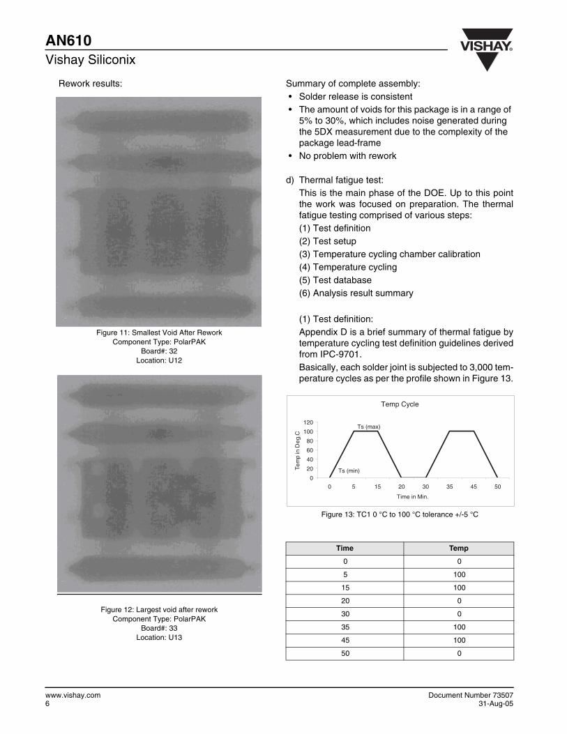
Figure 11: Smallest Void After ReworkComponent Type: PolarPAK
Board#: 32Location: U12
Figure 12: Largest void after reworkComponent Type: PolarPAK
Board#: 33Location: U13
Figure 13: TC1 0 °C to 100 °C tolerance +/-5 °C
Time Temp
0 0
5 100
15 100
20 0
30 0
35 100
45 100
50 0
Temp Cycle
0
20
40
60
80
100
120
0 5 15 20 30 35 45 50
Time in Min.
Tem
p in
Deg
.C
Ts (max)
Ts (min)

Vishay SiliconixAN610
Document Number 7350731-Aug-05
www.vishay.com7
If any solder joint failure occurs, it is detected by com-paring the joint resistance and is recoded withrespect to the cycle number in which it occurred.
(2) Test setup:A programmable temperature cycling chamber wasprogrammed for the temperature cycle shown in Fig-ure 13. The test chamber had a pre-wired card-cagethat could take multiple PCB assemblies conformingto the card-cage form-factor. Each daisy chain wasconnected to an analysis-tech event detector sys-tem. The latter device compared, at a preset intervalof one cycle time during dwell-time, the resistancewith preset value 1 kΩ, and reported/recorded anevent any time the daisy chain resistance exceededthe preset value. Thus, even momentarily open cir-cuits were caught and reported.
(3) Temperature cycling chamber calibration:The temperature cycle chamber was calibrated for athermal mass of test load by measuring the actualtemperature profile on pertinent locations on the PCBassembly and component. Figure 14 shows the cali-brated profile used during the actual testing.
(4) Temperature cycling:The very first and last steps of the temperaturecycling test are measurements of daisy chain resis-tance. Appendix E is a tabulated record of each daisychain resistance before and after the temperaturecycling. The first resistance column is initial resis-tance and the second resistance column is the valueafter 3,000 cycles. PCB assemblies were loaded in the temperaturecycling chamber to begin the thermal fatigue test.
(5) Test databaseThe final test results are tabulated in the followingtable:Table 4: 3,000-Cycle Test Data
Figure 14: Calibration Profile
Vishay Board # 1 0 to 100°C
10 min. ramp and 10 min. dwell
-20-10
0102030405060708090
100110120
18:3
5
18:4
0
18:4
5
18:5
0
18:5
5
19:0
0
19:0
5
19:1
0
19:1
5
19:2
0
19:2
5
19:3
0
19:3
5
Time
Deg
rees
C
TC 15
Started 11/17/2004 Terminated 3/2/2005
Board Package Side ID Fail
29 PolarPAK U9
29 PolarPAK U10
29 PolarPAK U11
29 PolarPAK U12
29 PolarPAK U13
29 PolarPAK U14
29 PolarPAK U15
29 n/a U16 N/A
31 PolarPAK U9
31 PolarPAK U10
31 PolarPAK U11
31 PolarPAK U12
31 PolarPAK U13
31 PolarPAK U14
31 PolarPAK U15
31 n/a U16 N/A
32 PolarPAK U9
32 PolarPAK U10
32 PolarPAK U11
32 PolarPAK U12
32 PolarPAK U13
32 PolarPAK U14
32 PolarPAK U15
32 n/a U16 N/A
33 PolarPAK U9
33 PolarPAK U10
33 PolarPAK U11
33 PolarPAK U12
33 PolarPAK U13
33 PolarPAK U14
33 PolarPAK U15
33 n/a U16 N/A
34 PPAK SO8-EXT U1
34 PPAK SO8-EXT U2
34 PPAK SO8-EXT U3
34 PPAK SO8-EXT U4
34 PPAK SO8-EXT U5 t0
34 PPAK SO8-EXT U6

www.vishay.com8
Document Number 7350731-Aug-05
Vishay SiliconixAN610
(6) Results summary Table 5:
The above results show that the PolarPAK packagepasses the lead-free solder joint reliability test guide-lines as per IPC-9701
REFERENCE:[1] "Thermal fatigue analysis to study solder joint reliabil-
ity for new-generation SMD parts introduced byVishay Siliconix," by Serge Jaunay and KandarpPandya.
[2] IPC-9701 Standard for Solder Joint Reliability, anIPC publication.
[3] "Voiding: Occurrence and reliability issues with lead-free," by Martin Wickham, NPL.
[4] IPC-A-610D Criteria for Solder Joint Quality Inspec-tion.
34 PPAK SO8-EXT U7
34 n/a U8 N/A
34 PolarPAK U9
34 PolarPAK U10
34 PolarPAK U11
34 PolarPAK U12
34 PolarPAK U13
34 PolarPAK U14
34 PolarPAK U15
34 n/a U16 N/A
35 PolarPAK U9
35 PolarPAK U10
35 PolarPAK U11
35 PolarPAK U12
35 PolarPAK U13
35 PolarPAK U14
35 PolarPAK U15
35 n/a U16 N/A
Package First Fail # Failed % Failed
PolarPAK 0 0%
Started 11/17/2004 Terminated 3/2/2005
Board Package Side ID Fail
Vishay SiliconixAN610
Document Number 7350731-Aug-05
www.vishay.com9
Appendix A
POLARPAK X-Ray Images
After assembly (without rework)
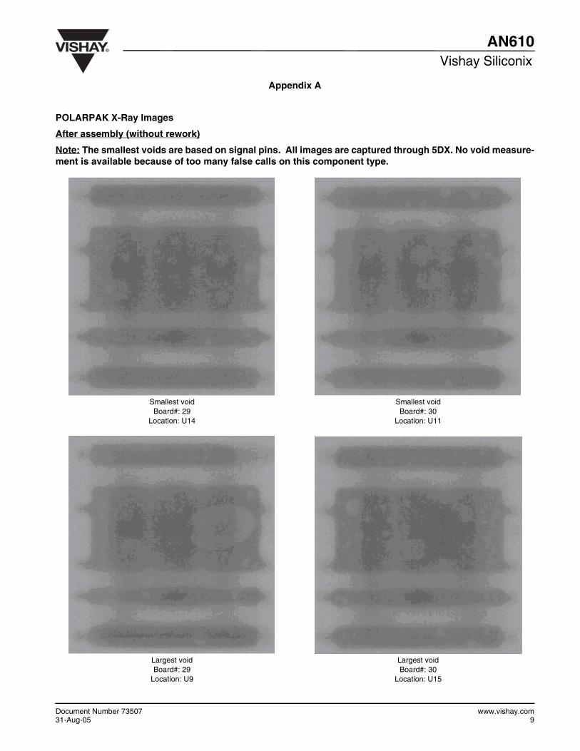
Note: The smallest voids are based on signal pins. All images are captured through 5DX. No void measure-ment is available because of too many false calls on this component type.
Smallest void Board#: 29
Location: U14
Largest voidBoard#: 29
Location: U9
Smallest void Board#: 30
Location: U11
Largest voidBoard#: 30
Location: U15

www.vishay.com10
Document Number 7350731-Aug-05
Vishay SiliconixAN610
Smallest void Board#: 31
Location: U11
Largest voidBoard#: 31
Location: U10
Smallest void Board#: 32
Location: U11
Largest voidBoard#: 32
Location: U14

Vishay SiliconixAN610
Document Number 7350731-Aug-05
www.vishay.com11
Smallest void Board#: 33
Location: U12
Largest voidBoard#: 33
Location: U9
Smallest void Board#: 34
Location: U13
Largest voidBoard#: 34
Location: U14

www.vishay.com12
Document Number 7350731-Aug-05
Vishay SiliconixAN610
Smallest void Board#: 35
Location: U12
Largest voidBoard#: 35
Location: U14

Vishay SiliconixAN610
Document Number 7350731-Aug-05
www.vishay.com13
Appendix B
PCB Layout
SMD125T16L_Ver C_Side A

www.vishay.com14
Document Number 7350731-Aug-05
Vishay SiliconixAN610
Appendix C
PCB Fabrication
Material: FR-4Thickness: 3.175 mm [0.125 in.]Number of copper layers: 16Nominal outer layer (top/bottom) cu thickness: 35 µm [1378 µin.] 0.5 oz.Nominal inner layer cu thickness: 12 µm [472 µin.] 0.5 oz.Nominal FR4 insulation layer thickness: 231.8 µm [7,709 µin.]Even internal layers 2, 4, 5, 7 from each side: Power and groundCu coverage on power/ground layers:70%Cu coverage on Signal trace: 40%Min. outer layer trace width: 150 µm [5906 µin.]Test pads for each daisy chain to be providedMinimum 15-mm [0.6-in.] clearance around each part for rework and if necessary the removal of the failed part with-out damage to the adjacent part/traceMinimum via for large (drain) land pad:50%Via size: Pitch: 1.0 mm [0.040 in.]
Diameter: 0.3 mm [0.012 in.]Solder mask encroachment on the via pad for these via on the bottom side to prevent the solder from spreading onthe bottom side.Square test pad size: 1.5 mm [0.060 in.]
PTH Drill: 1.0 mm [0.040 in.]Surface finish: (preferred)OSP (Organic Solderability Preservative)
Silkscreen or Cu etch to label all components, all test points, and location of pin is mandated.

Vishay SiliconixAN610
Document Number 7350731-Aug-05
www.vishay.com15
Appendix D
Performance and Reliability of Solder Joints for Vishay Siliconix SMD Part Package -- PolarPAK
Scope of work for temperature cycling
Using IPC-9701 guidelines
Test sample size distribution: Total number of test vehicles (PCBs): 6 (+1 reference board)Total number of daisy chains: 42 (+7 on reference board)
Variety of PCBs - lead-free assemblies:PCB #SMD125T16L Ver_C Side A 6 (+1 reference board) Number of PolarPAK parts on each PCB: 7Number of PolarPAK daisy chains per PCB: 7
Number of parts reworked: 10 (+2 on reference board)Number of parts reworked per PCB: 2 for 6 out of 7 test boards (including reference board)
Temperature cycle definition: TC1 0 °C to 100 °C tolerance +/-5 °C
Temperature ramp rate: 20 °C/minutesHigh temperature dwell: 10 minutesLow temperature dwell: 10 minutes
Test duration:Whichever condition occurs first:
50% cumulative failureorNumber of thermal cycles: NTC-D 3,000 cyclesIn case of failure continue testing up to 6,000 cycles or 50% cumulative failures, whichever occurs first.
Temp Cycle
0
20
40
60
80
100
120
0 5 15 20 30 35 45 50
Time in Min.
Tem
p in
Deg
.C
Ts (max)
Ts (min)
Time Temp
0 0
5 100
15 100
20 0
30 0
35 100
45 100
50 0

www.vishay.com16
Document Number 7350731-Aug-05
Vishay SiliconixAN610
Test monitoring: Event detector or continuous monitoring of electrical resistance of each daisy chain
Temperature chamber characterization:Component temperature to be monitored and recorded at each board location in the chamber during the initial setup.Characterization should be performed using a representative sample load, test board configuration, and fixtures.
Failure definition: Event detector 1,000 W, 10 events (maximum), 1 µs duration (maximum), reports first verified as time-to-failure.and/orData logger/voltmeter: 20% nominal resistance increase (maximum), five readings/scans (maximum)
Data documentation:1. Detailed description of all experimental apparatus, including thermal chamber and data acquisition system2. Temperature vs. time plots for both the board and chamber including the chamber setup characterization data3. Resistance vs. time plot for data logger samples4. Tabular data for the number of cycles to failure for all failures5. Weibull analysis

Vishay SiliconixAN610
Document Number 7350731-Aug-05
www.vishay.com17
Appendix EContinuity TestBoard#: 029 (Lead-Free) Rev: C / Side: A
Comp RefPackage
typeRes (Ohm) Res (Ohm) Note
U16 PolarPAK Open Open No component
U15 PolarPAK 0.209 0.229
U14 PolarPAK 0.317 0.336
U13 PolarPAK 0.433 0.451
U12 PolarPAK 0.072 0.088
U11 PolarPAK 0.217 0.229 X’ (Rework)
U10 PolarPAK 0.305 0.305 X’ (Rework)
U9 PolarPAK 0.406 0.407
Board#: 030 (Lead-Free) Rev: C / Side: A
Comp RefPackage
typeRes (Ohm) Res (Ohm) Note
U16 PolarPAK Open Open No component
U15 PolarPAK 0.201 0.202 X’ (Rework)
U14 PolarPAK 0.303 0.306
U13 PolarPAK 0.425 0.417
U12 PolarPAK 0.065 0.057
U11 PolarPAK 0.213 0.205 X’ (Rework)
U10 PolarPAK 0.297 0.317
U9 PolarPAK 0.401 0.413
Board#: 031 (Lead-Free) Rev: C / Side: A
Comp RefPackage
typeRes (Ohm) Res (Ohm) Note
U16 PolarPAK Open Open No component
U15 PolarPAK 0.206 0.202 X’ (Rework)
U14 PolarPAK 0.307 0.302
U13 PolarPAK 0.425 0.422
U12 PolarPAK 0.068 0.066 X’ (Rework)
U11 PolarPAK 0.214 0.247
U10 PolarPAK 0.296 0.303
U9 PolarPAK 0.399 0.403
Board#: 032 (Lead-Free) Rev: C / Side: A
Comp RefPackage
typeRes (Ohm) Res (Ohm) Note
U16 PolarPAK Open Open No component
U15 PolarPAK 0.201 0.239
U14 PolarPAK 0.305 0.344
U13 PolarPAK 0.421 0.456
Board#: 032 (Lead-Free) Rev: C / Side: A
Comp RefPackage
typeRes (Ohm) Res (Ohm) Note
U12 PolarPAK 0.061 0.092 X’ (Rework)
U11 PolarPAK 0.207 0.233 X’ (Rework)
U10 PolarPAK 0.291 0.316
U9 PolarPAK 0.393 0.415
Board#: 033 (Lead-Free) Rev: C / Side: A
Comp RefPackage
typeRes (Ohm) Res (Ohm) Note
U16 PolarPAK Open Open No component
U15 PolarPAK 0.198 0.229
U14 PolarPAK 0.304 0.336 X’ (Rework)
U13 PolarPAK 0.415 0.443 X’ (Rework)
U12 PolarPAK 0.059 0.084
U11 PolarPAK 0.207 0.233
U10 PolarPAK 0.293 0.301
U9 PolarPAK 0.391 0.399
Board#: 034 (Lead-Free) Rev: C / Side: A
Comp RefPackage
typeRes (Ohm) Res (Ohm) Note
U16 PolarPAK Open Open No component
U15 PolarPAK 0.201 0.229
No
U14 PolarPAK 0.304 0.321
U13 PolarPAK 0.415 0.438
U12 PolarPAK 0.063 0.086
U11 PolarPAK 0.209 0.228
U10 PolarPAK 0.292 0.309
U9 PolarPAK 0.394 0.410
Board#: 035 (Lead-Free) Rev: C / Side: A
Comp RefPackage
typeRes (Ohm) Res (Ohm) Note
U16 PolarPAK Open Open No component
U15 PolarPAK 0.205 0.215
U14 PolarPAK 0.312 0.311
U13 PolarPAK 0.426 0.424
U12 PolarPAK 0.066 0.053 X’ (Rework)
U11 PolarPAK 0.215 0.214
U10 PolarPAK 0.300 0.295 X’ (Rework)
U9 PolarPAK 0.399 0.398