Pnr Tutorial
17
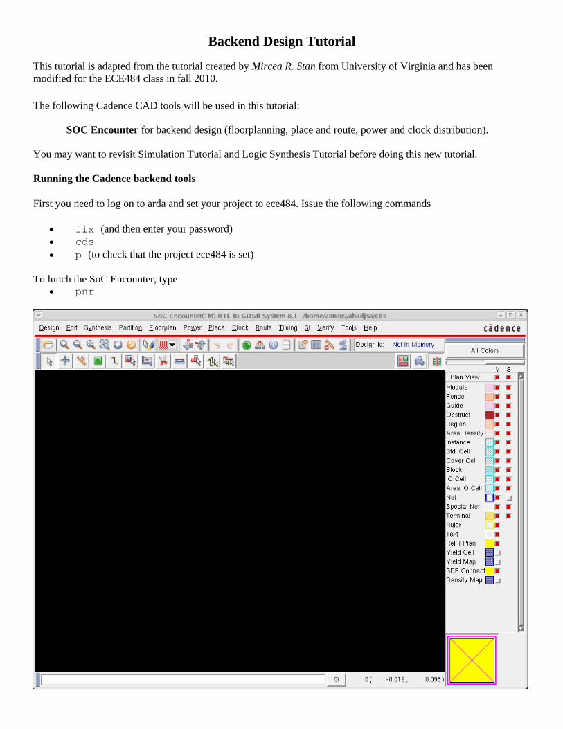
Backend Design Tutorial This tutorial is adapted from the tutorial created by Mircea R. Stan from University of Virginia and has been modified for the ECE484 class in fall 2010. The following Cadence CAD tools will be used in this tutorial: SOC Encounter for backend design (floorplanning, place and route, power and clock distribution). You may want to revisit Simulation Tutorial and Logic Synthesis Tutorial before doing this new tutorial. Running the Cadence backend tools First you need to log on to arda and set your project to ece484. Issue the following commands • fix (and then enter your password) • cds • p (to check that the project ece484 is set) To lunch the SoC Encounter, type • pnr
-
Upload
narashimaraja -
Category
Documents
-
view
264 -
download
2
description
Place and Routing using soc encounter
Transcript of Pnr Tutorial
Backend Design Tutorial
This tutorial is adapted from the tutorial created by Mircea R. Stan from University of Virginia and has been modified for the ECE484 class in fall 2010. The following Cadence CAD tools will be used in this tutorial:
SOC Encounter for backend design (floorplanning, place and route, power and clock distribution).
You may want to revisit Simulation Tutorial and Logic Synthesis Tutorial before doing this new tutorial. Running the Cadence backend tools
First you need to log on to arda and set your project to ece484. Issue the following commands
• fix (and then enter your password) • cds • p (to check that the project ece484 is set)
To lunch the SoC Encounter, type
• pnr
The window has three main areas:
• Menu Bar (top) • Select Bar (right) • Display Area (middle)
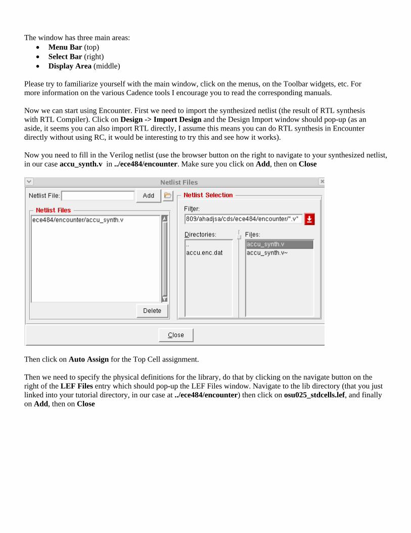
Please try to familiarize yourself with the main window, click on the menus, on the Toolbar widgets, etc. For more information on the various Cadence tools I encourage you to read the corresponding manuals. Now we can start using Encounter. First we need to import the synthesized netlist (the result of RTL synthesis with RTL Compiler). Click on Design -> Import Design and the Design Import window should pop-up (as an aside, it seems you can also import RTL directly, I assume this means you can do RTL synthesis in Encounter directly without using RC, it would be interesting to try this and see how it works). Now you need to fill in the Verilog netlist (use the browser button on the right to navigate to your synthesized netlist, in our case accu_synth.v in ../ece484/encounter. Make sure you click on Add, then on Close
Then click on Auto Assign for the Top Cell assignment. Then we need to specify the physical definitions for the library, do that by clicking on the navigate button on the right of the LEF Files entry which should pop-up the LEF Files window. Navigate to the lib directory (that you just linked into your tutorial directory, in our case at ../ece484/encounter) then click on osu025_stdcells.lef, and finally on Add, then on Close
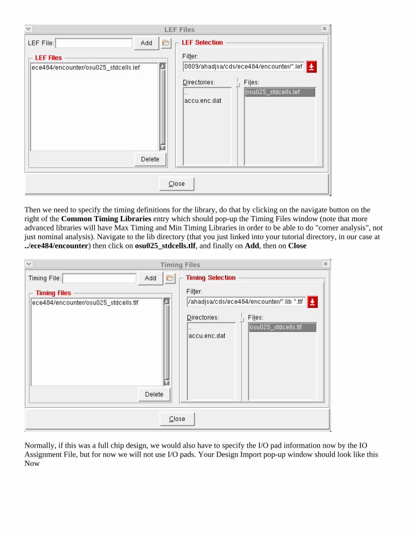
Then we need to specify the timing definitions for the library, do that by clicking on the navigate button on the right of the Common Timing Libraries entry which should pop-up the Timing Files window (note that more advanced libraries will have Max Timing and Min Timing Libraries in order to be able to do "corner analysis", not just nominal analysis). Navigate to the lib directory (that you just linked into your tutorial directory, in our case at ../ece484/encounter) then click on osu025_stdcells.tlf, and finally on Add, then on Close
Normally, if this was a full chip design, we would also have to specify the I/O pad information now by the IO Assignment File, but for now we will not use I/O pads. Your Design Import pop-up window should look like this Now
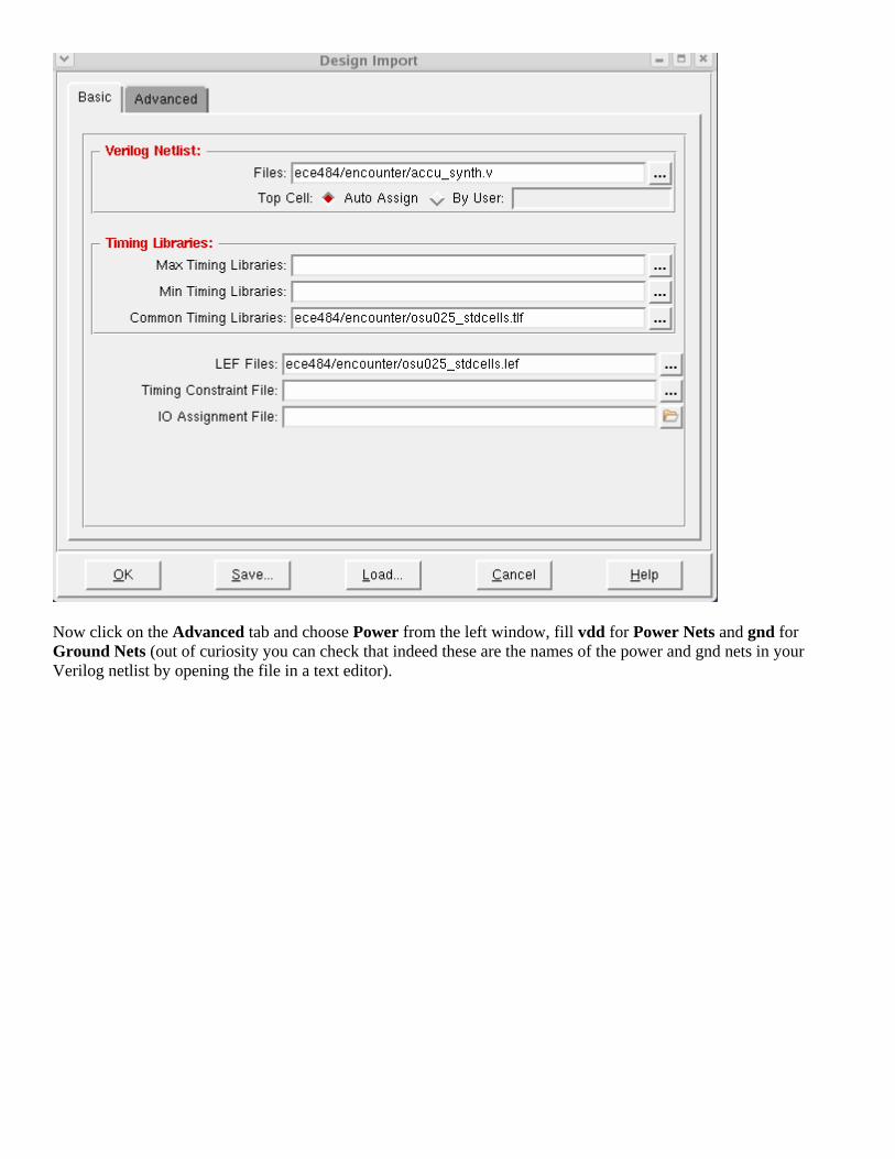
Now click on the Advanced tab and choose Power from the left window, fill vdd for Power Nets and gnd for Ground Nets (out of curiosity you can check that indeed these are the names of the power and gnd nets in your Verilog netlist by opening the file in a text editor).
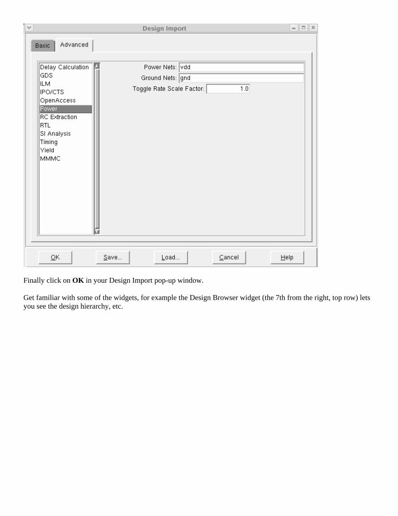
Finally click on OK in your Design Import pop-up window. Get familiar with some of the widgets, for example the Design Browser widget (the 7th from the right, top row) lets you see the design hierarchy, etc.
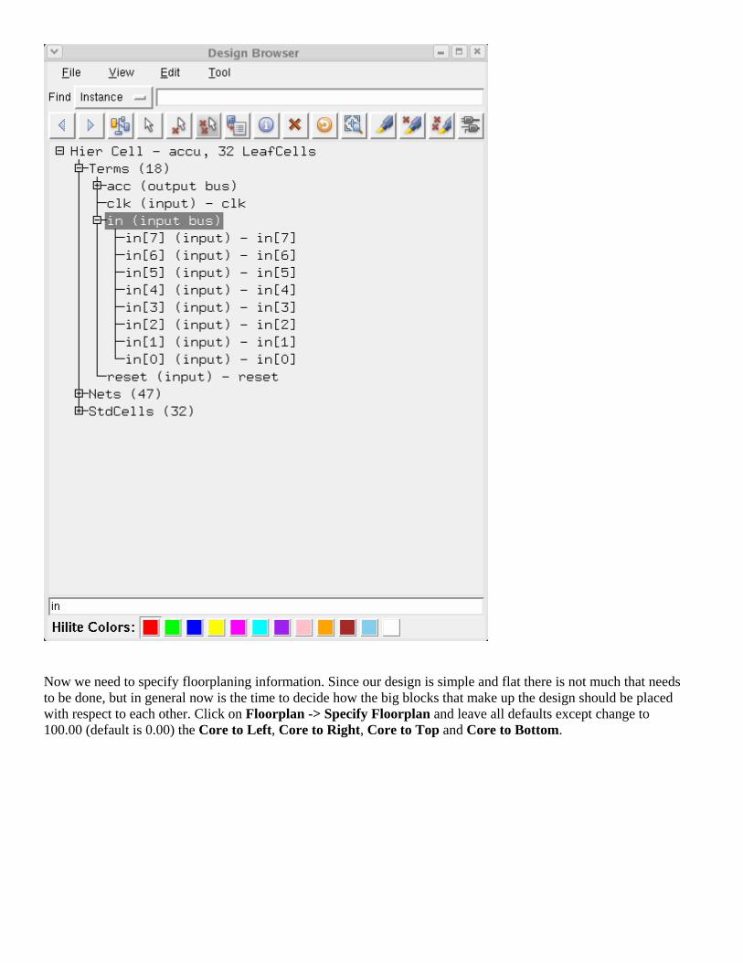
Now we need to specify floorplaning information. Since our design is simple and flat there is not much that needs to be done, but in general now is the time to decide how the big blocks that make up the design should be placed with respect to each other. Click on Floorplan -> Specify Floorplan and leave all defaults except change to 100.00 (default is 0.00) the Core to Left, Core to Right, Core to Top and Core to Bottom.
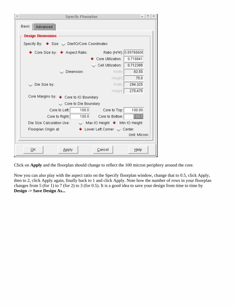
Click on Apply and the floorplan should change to reflect the 100 micron periphery around the core. Now you can also play with the aspect ratio on the Specify floorplan window, change that to 0.5, click Apply, then to 2, click Apply again, finally back to 1 and click Apply. Note how the number of rows in your floorplan changes from 5 (for 1) to 7 (for 2) to 3 (for 0.5). It is a good idea to save your design from time to time by Design -> Save Design As...
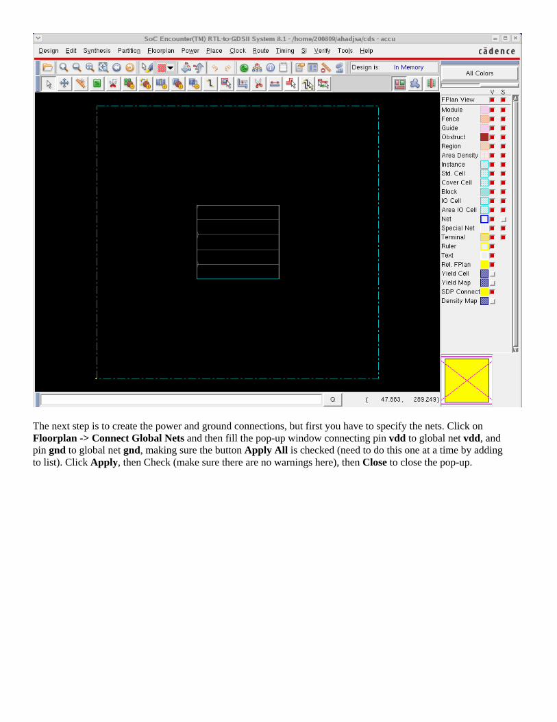
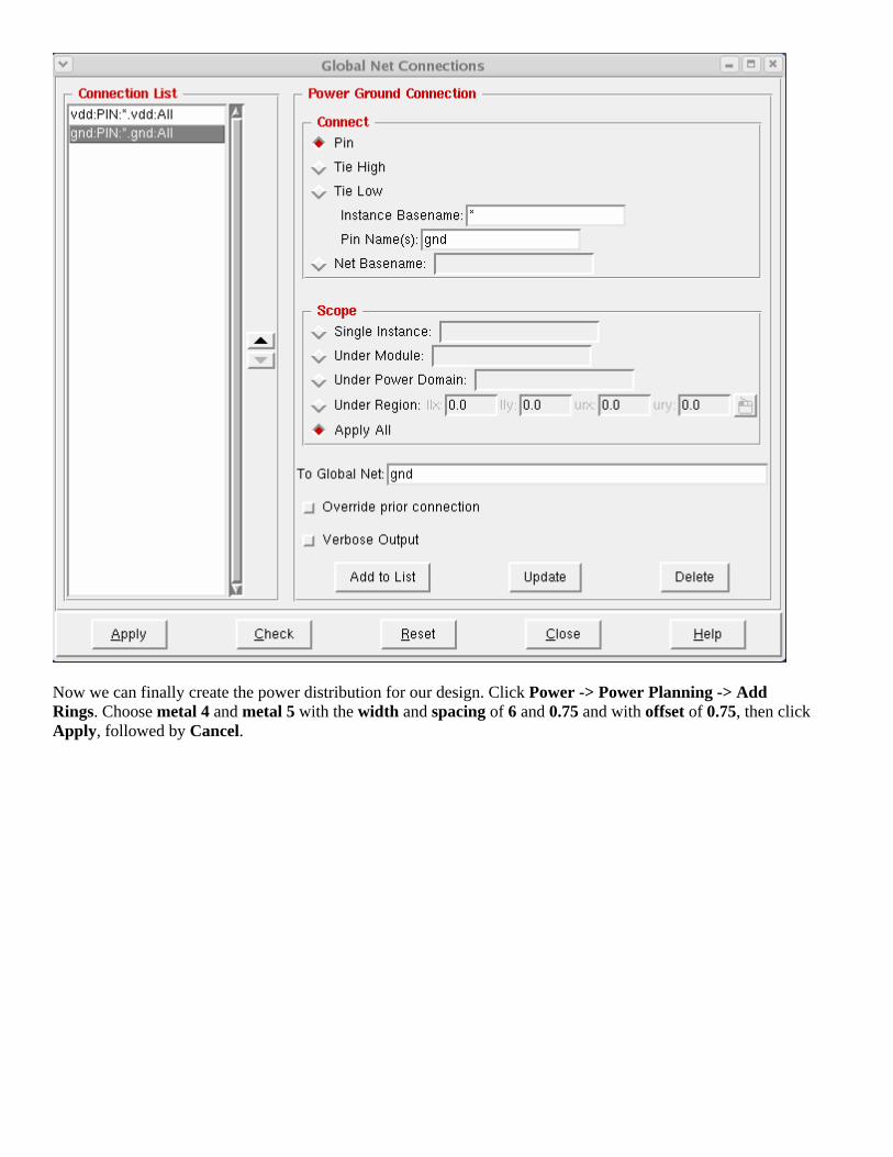
The next step is to create the power and ground connections, but first you have to specify the nets. Click on Floorplan -> Connect Global Nets and then fill the pop-up window connecting pin vdd to global net vdd, and pin gnd to global net gnd, making sure the button Apply All is checked (need to do this one at a time by adding to list). Click Apply, then Check (make sure there are no warnings here), then Close to close the pop-up.
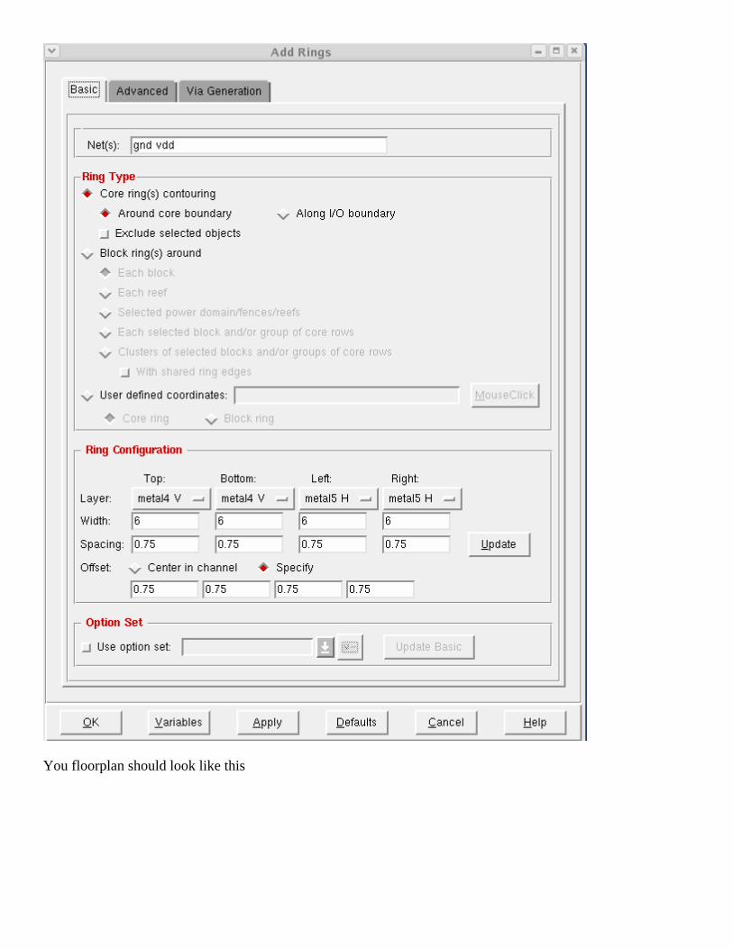
Now we can finally create the power distribution for our design. Click Power -> Power Planning -> Add Rings. Choose metal 4 and metal 5 with the width and spacing of 6 and 0.75 and with offset of 0.75, then click Apply, followed by Cancel.
You floorplan should look like this
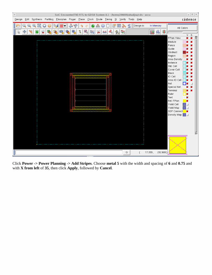
Click Power -> Power Planning -> Add Stripes. Choose metal 5 with the width and spacing of 6 and 0.75 and with X from left of 35, then click Apply, followed by Cancel.
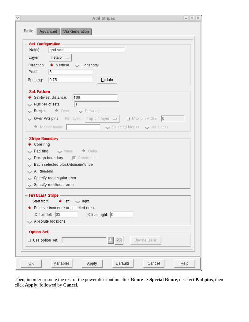
Then, in order to route the rest of the power distribution click Route -> Special Route, deselect Pad pins, then click Apply, followed by Cancel.
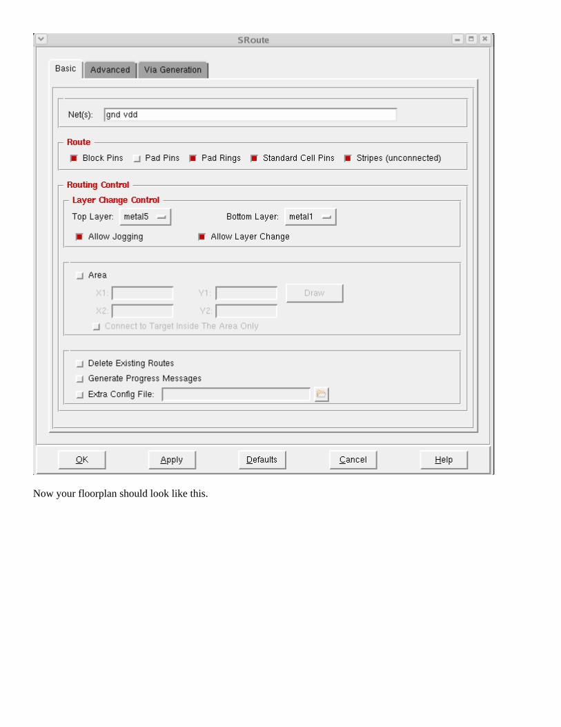
Now your floorplan should look like this.
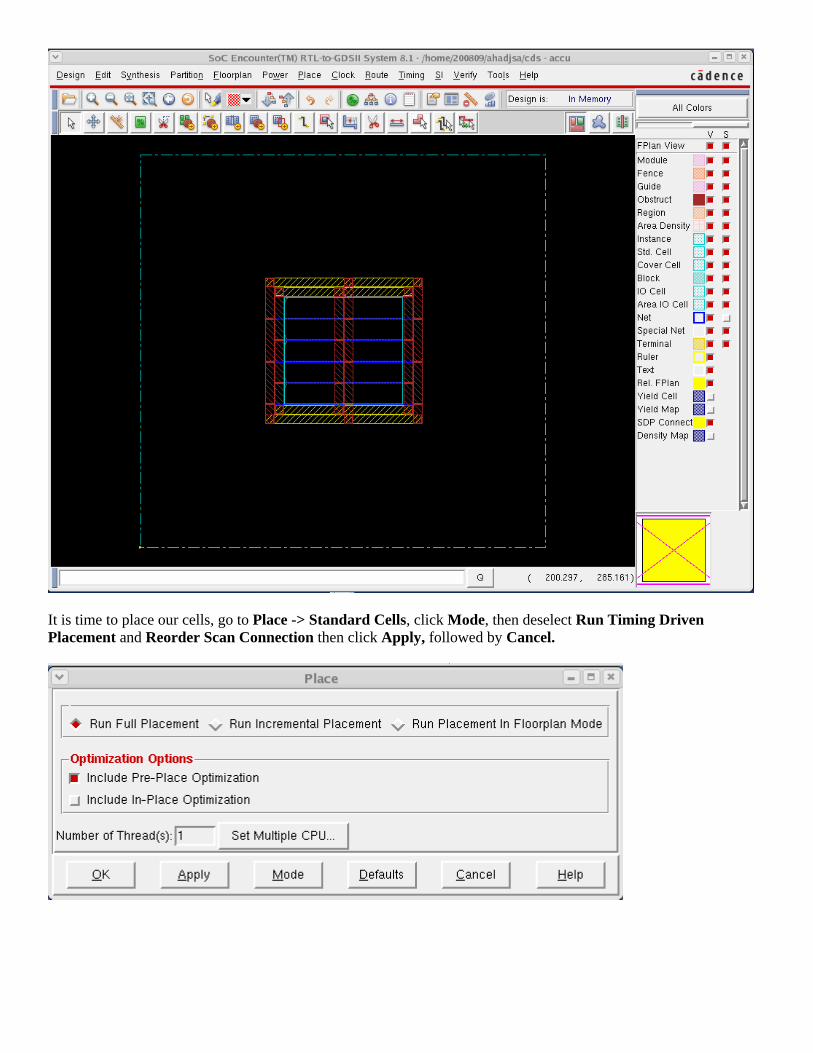
It is time to place our cells, go to Place -> Standard Cells, click Mode, then deselect Run Timing Driven Placement and Reorder Scan Connection then click Apply, followed by Cancel.
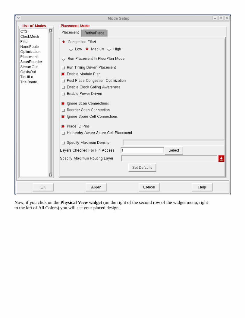
Now, if you click on the Physical View widget (on the right of the second row of the widget menu, right to the left of All Colors) you will see your placed design.
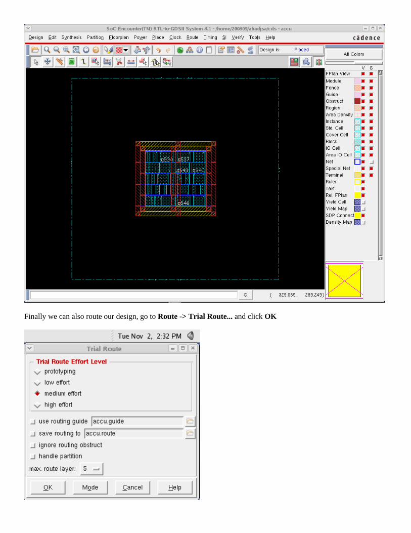
Finally we can also route our design, go to Route -> Trial Route... and click OK
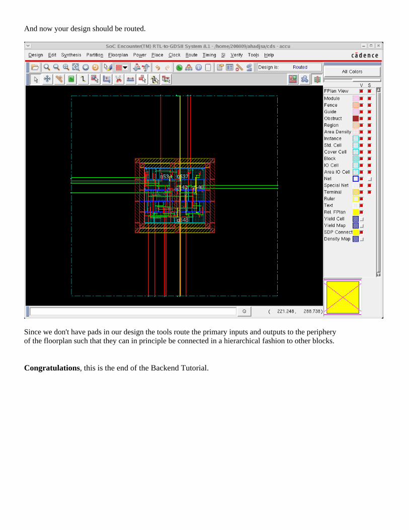
And now your design should be routed.
Since we don't have pads in our design the tools route the primary inputs and outputs to the periphery of the floorplan such that they can in principle be connected in a hierarchical fashion to other blocks. Congratulations, this is the end of the Backend Tutorial.