PMP10655 Test Results - TI.com
33
Test Report PMP10655 1 January 27, 2016 Test Data For PMP10655 January 27, 2016
Transcript of PMP10655 Test Results - TI.com

Test Report PMP10655
1 January 27, 2016
Test Data
For PMP10655
January 27, 2016

Test Report PMP10655
2 January 27, 2016
Table of Contents 1. Design Specifications ............................................................................................................................ 3
2. Circuit Description ................................................................................................................................. 3
3. PMP10655 Board Photos ...................................................................................................................... 4
4. Thermal Data ......................................................................................................................................... 5
5. Efficiency ............................................................................................................................................... 7
5.1 Efficiency Graph .................................................................................................................................. 7
5.2 Efficiency Data..................................................................................................................................... 8
6 Waveforms ................................................................................................................................................. 9
6.1 Load Transient Response .................................................................................................................... 9
6.2 Startup .............................................................................................................................................. 15
6.3 Output Voltage Ripple and Switch Node Voltages ........................................................................... 21
6.4 Short Circuit Test ............................................................................................................................... 27
6.5 Line Transient Tests .......................................................................................................................... 29

Test Report PMP10655
3 January 27, 2016
1. Design Specifications Vin Minimum 6VDC (4.3Vin Cold-Crank Dip)
Vin Nominal 12VDC
Vin Maximum 18VDC (42Vin Load Dump Peak)
Vout1 and Vout2 3.8VDC
Iout1 and Iout2 8A Max. Continuous Each (14A Peak Each)
Nominal Switching Frequency (Fsw1 and Fsw2) 2.2MHz
2. Circuit Description PMP10655 is a Dual-Output Synchronous Buck Converter using the LM5140 controller IC. The design accepts an input voltage between 6Vin and 18Vin and is capable of supplying a maximum of 8A of continuous current (14A Peak) to the load, per output. Vout1 and Vout2 maintain regulation during cold-crank (Vin dip to 4.3Vin) and load-dump (Vin peak to 42Vin) conditions. Switching of the two converters are 180 degrees out of phase between each other. The design also features the LM5050-1 OR-ing controller configured for efficient reverse polarity protection of the input. PMP10655 is built on a 4-layer FR-4 PCB, with 2 oz. Copper on the Top and Bottom layers, and 1 oz. Copper on the two internal layers. All tests were performed with an external 5V supply connected to VCCX. VCCX and the enable inputs of
both channels were ganged together.

Test Report PMP10655
4 January 27, 2016
3. PMP10655 Board Photos Board Dimensions: 6.285” x 2.845”
Board Photo (Top View)
Board Photo (Bottom View)

Test Report PMP10655
5 January 27, 2016
4. Thermal Data
IR thermal image taken at steady state with 12Vin and 8A load on each output channel (no airflow;
ambient at room temp.)

Test Report PMP10655
6 January 27, 2016
IR thermal image taken at steady state with 12Vin and 8A load on each output channel (zoomed
image of controller; no airflow; ambient at room temp.)

Test Report PMP10655
7 January 27, 2016
5. Efficiency
5.1 Efficiency Graph
78.0
80.0
82.0
84.0
86.0
88.0
90.0
92.0
94.0
96.0
10 20 30 40 50 60 70 80 90 100
Effi
cie
ncy
(%
)
Load Current (% of Full Load; Full Load is 8A on each output)
PMP10655 Efficiency
Efficiency @ 6Vin
Efficiency @ 12Vin
Efficiency @ 18Vin

Test Report PMP10655
8 January 27, 2016
5.2 Efficiency Data
Vin (V)
Iin (A)
Vout1 (V)
Iout1 (A)
Vout2 (V)
Iout2 (A)
Pin (W)
Pout1 (W)
Pout2 (W)
Pout Total (W)
Ploss (W)
Efficiency (%)
% of Full Load
6 1.086 3.8155 0.8001 3.8139 0.8 6.516 3.053 3.051 6.104 0.412 93.7 10
6 2.161 3.8155 1.6007 3.8137 1.603 12.966 6.107 6.113 12.221 0.745 94.3 20
6 3.238 3.8156 2.4001 3.8136 2.401 19.428 9.158 9.156 18.314 1.114 94.3 30
6 4.328 3.8156 3.1998 3.8135 3.198 25.968 12.209 12.196 24.405 1.563 94.0 40
6 5.438 3.8155 4.0009 3.8132 4.01 32.628 15.265 15.291 30.556 2.072 93.7 50
6 6.545 3.8154 4.8004 3.813 4.8005 39.270 18.315 18.304 36.620 2.650 93.3 60
6 7.669 3.8155 5.6 3.8129 5.599 46.014 21.367 21.348 42.715 3.299 92.8 70
6 8.813 3.8155 6.3991 3.8128 6.404 52.878 24.416 24.417 48.833 4.045 92.4 80
6 9.97 3.8158 7.2087 3.8128 7.2 59.820 27.507 27.452 54.959 4.861 91.9 90
6 11.16 3.8158 8.0065 3.8128 8.016 66.930 30.551 30.563 61.115 5.815 91.3 100
Vin (V)
Iin (A)
Vout1 (V)
Iout1 (A)
Vout2 (V)
Iout2 (A)
Pin (W)
Pout1 (W)
Pout2 (W)
Pout Total (W)
Ploss (W)
Efficiency (%)
% of Full Load
12 0.589 3.8156 0.8 3.814 0.8 7.068 3.052 3.051 6.104 0.964 86.4 10
12 1.139 3.8154 1.6008 3.8137 1.6 13.668 6.108 6.102 12.210 1.458 89.3 20
12 1.693 3.8153 2.4003 3.8136 2.401 20.316 9.158 9.156 18.314 2.002 90.1 30
12 2.253 3.8152 3.2001 3.8135 3.207 27.036 12.209 12.230 24.439 2.597 90.4 40
12 2.82 3.8149 4.0012 3.8132 4.003 33.840 15.264 15.264 30.528 3.312 90.2 50
12 3.392 3.8148 4.8009 3.8129 4.801 40.704 18.314 18.306 36.620 4.084 90.0 60
12 3.974 3.8146 5.6008 3.8127 5.602 47.688 21.365 21.359 42.724 4.964 89.6 70
12 4.56 3.8145 6.4002 3.8125 6.401 54.720 24.414 24.404 48.817 5.903 89.2 80
12 5.158 3.8144 7.2098 3.8123 7.203 61.896 27.501 27.460 54.961 6.935 88.8 90
12 5.77 3.8139 8.0077 3.8118 8.007 69.240 30.541 30.521 61.062 8.178 88.2 100
Vin (V)
Iin (A)
Vout1 (V)
Iout1 (A)
Vout2 (V)
Iout2 (A)
Pin (W)
Pout1 (W)
Pout2 (W)
Pout Total (W)
Ploss (W)
Efficiency (%)
% of Full Load
18 0.43 3.816 0.8002 3.8144 0.8015 7.740 3.054 3.057 6.111 1.629 79.0 10
18 0.811 3.8156 1.5999 3.8139 1.595 14.598 6.105 6.083 12.188 2.410 83.5 20
18 1.193 3.8155 2.4011 3.8138 2.398 21.474 9.161 9.145 18.307 3.167 85.3 30
18 1.582 3.8152 3.1999 3.8135 3.199 28.476 12.208 12.199 24.408 4.068 85.7 40
18 1.975 3.8149 4.0012 3.8132 4.001 35.550 15.264 15.257 30.521 5.029 85.9 50
18 2.374 3.8146 4.801 3.8129 4.802 42.732 18.314 18.310 36.623 6.109 85.7 60
18 2.778 3.8143 5.602 3.8126 5.602 50.004 21.368 21.358 42.726 7.278 85.4 70
18 3.18 3.8143 6.4009 3.8124 6.402 57.240 24.415 24.407 48.822 8.418 85.3 80
18 3.588 3.814 7.21 3.8121 7.202 64.584 27.499 27.455 54.954 9.630 85.1 90
18 3.995 3.8138 8.007 3.8118 8.022 71.910 30.537 30.578 61.115 10.795 85.0 100

Test Report PMP10655
9 January 27, 2016
6 Waveforms
6.1 Load Transient Response
Load Transient Response on Vout1 at 6Vin and 0.8A-to-8A (10%-to-100%) Load Step with Vout2
Loaded at a Constant 8A

Test Report PMP10655
10 January 27, 2016
Load Transient Response on Vout1 at 12Vin and 0.8A-to-8A (10%-to-100%) Load Step with Vout2
Loaded at a Constant 8A

Test Report PMP10655
11 January 27, 2016
Load Transient Response on Vout1 at 18Vin and 0.8A-to-8A (10%-to-100%) Load Step with Vout2
Loaded at a Constant 8A

Test Report PMP10655
12 January 27, 2016
Load Transient Response on Vout2 at 6Vin and 0.8A-to-8A (10%-to-100%) Load Step with Vout1
Loaded at a Constant 8A
Test Report PMP10655
13 January 27, 2016
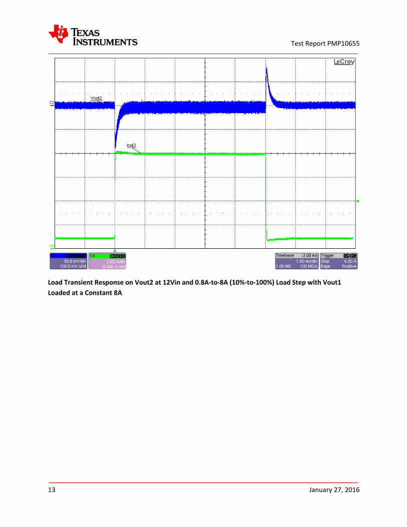
Load Transient Response on Vout2 at 12Vin and 0.8A-to-8A (10%-to-100%) Load Step with Vout1
Loaded at a Constant 8A

Test Report PMP10655
14 January 27, 2016
Load Transient Response on Vout2 at 18Vin and 0.8A-to-8A (10%-to-100%) Load Step with Vout1
Loaded at a Constant 8A

Test Report PMP10655
15 January 27, 2016
6.2 Startup
Startup into No Load at 6Vin (both outputs unloaded)

Test Report PMP10655
16 January 27, 2016
Startup into Full Load at 6Vin (both outputs loaded at 8A each)

Test Report PMP10655
17 January 27, 2016
Startup into No Load at 12Vin (both outputs unloaded)

Test Report PMP10655
18 January 27, 2016
Startup into Full Load at 12Vin (both outputs loaded at 8A each)

Test Report PMP10655
19 January 27, 2016
Startup into No Load at 18Vin (both outputs unloaded)

Test Report PMP10655
20 January 27, 2016
Startup into Full Load at 18Vin (both outputs loaded at 8A each)

Test Report PMP10655
21 January 27, 2016
6.3 Output Voltage Ripple and Switch Node Voltages
Switch Node Voltages at 6Vin and 8A Load on Each Output

Test Report PMP10655
22 January 27, 2016
Switch Node Voltages at 12Vin and 8A Load on Each Output

Test Report PMP10655
23 January 27, 2016
Switch Node Voltages at 18Vin and 8A Load on Each Output

Test Report PMP10655
24 January 27, 2016
Output Voltage Ripple at 6Vin and 8A Load on Each Output (Vripple ≈ 15mVp-p)

Test Report PMP10655
25 January 27, 2016
Output Voltage Ripple at 12Vin and 8A Load on Each Output (Vripple ≈ 20mVp-p)

Test Report PMP10655
26 January 27, 2016
Output Voltage Ripple at 18Vin and 8A Load on Each Output (Vripple ≈ 25mVp-p)
Test Report PMP10655
27 January 27, 2016
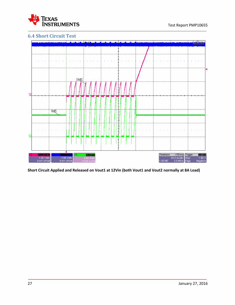
6.4 Short Circuit Test
Short Circuit Applied and Released on Vout1 at 12Vin (both Vout1 and Vout2 normally at 8A Load)

Test Report PMP10655
28 January 27, 2016
Short Circuit Applied and Released on Vout2 at 12Vin (both Vout1 and Vout2 normally at 8A Load)

Test Report PMP10655
29 January 27, 2016
6.5 Line Transient Tests
Line Transient from 12Vin to 4.3Vin with Both Outputs Loaded at 8A Each

Test Report PMP10655
30 January 27, 2016
Line Transient from 4.3Vin to 12Vin with Both Outputs Loaded at 8A Each

Test Report PMP10655
31 January 27, 2016
Line Transient from 12Vin to 42Vin with Both Outputs Loaded at 8A Each

Test Report PMP10655
32 January 27, 2016
Line Transient from 42Vin to 12Vin with Both Outputs Loaded at 8A Each

IMPORTANT NOTICE AND DISCLAIMERTI PROVIDES TECHNICAL AND RELIABILITY DATA (INCLUDING DATASHEETS), DESIGN RESOURCES (INCLUDING REFERENCEDESIGNS), APPLICATION OR OTHER DESIGN ADVICE, WEB TOOLS, SAFETY INFORMATION, AND OTHER RESOURCES “AS IS”AND WITH ALL FAULTS, AND DISCLAIMS ALL WARRANTIES, EXPRESS AND IMPLIED, INCLUDING WITHOUT LIMITATION ANYIMPLIED WARRANTIES OF MERCHANTABILITY, FITNESS FOR A PARTICULAR PURPOSE OR NON-INFRINGEMENT OF THIRDPARTY INTELLECTUAL PROPERTY RIGHTS.These resources are intended for skilled developers designing with TI products. You are solely responsible for (1) selecting the appropriateTI products for your application, (2) designing, validating and testing your application, and (3) ensuring your application meets applicablestandards, and any other safety, security, or other requirements. These resources are subject to change without notice. TI grants youpermission to use these resources only for development of an application that uses the TI products described in the resource. Otherreproduction and display of these resources is prohibited. No license is granted to any other TI intellectual property right or to any third partyintellectual property right. TI disclaims responsibility for, and you will fully indemnify TI and its representatives against, any claims, damages,costs, losses, and liabilities arising out of your use of these resources.TI’s products are provided subject to TI’s Terms of Sale (https:www.ti.com/legal/termsofsale.html) or other applicable terms available eitheron ti.com or provided in conjunction with such TI products. TI’s provision of these resources does not expand or otherwise alter TI’sapplicable warranties or warranty disclaimers for TI products.IMPORTANT NOTICE
Mailing Address: Texas Instruments, Post Office Box 655303, Dallas, Texas 75265Copyright © 2021, Texas Instruments Incorporated