PMLK Buck-Boost Experiment Book (Rev. A) - TI
87
SSQU009A PMLKBUCKBOOSTEVM REV A TI-PMLK TI Power Management Lab Kit Buck-Boost Experiment Book
Transcript of PMLK Buck-Boost Experiment Book (Rev. A) - TI

SSQU009APMLKBUCKBOOSTEVM REV A
TI-PMLKTI Power Management Lab KitBuck-Boost Experiment Book


3 | TI Power Management Lab Kit Texas Instruments
Name
University/Company name
Address
Phone


5 | TI Power Management Lab Kit Texas Instruments
Many people have collaborated with me in the realization of
the TI-PMLK project, in different times, at different levels, in
different ways. My sincerest thanks go to the Texas Instruments
University Program Team and to the University of Salerno
Power Electronics Laboratory Team.
Nicola Femia


7 | TI Power Management Lab Kit Texas Instruments
PrefaceFelix, qui potuit rerum cognoscere causas...
(Happy, he who could capture the origins of things...)Publio Virgilio Marone, Mantova 70 B.C. – Brindisi 19 B.C.
Design is an exciting and fascinating art. Power electronics, for its interdisciplinarily nature, is a challenging field where the knowledge of why makes all the difference in understanding how to achieve design goals. The will of learning and the means
for learning are the two basic ingredients needed to develop the virtuous ability to understand the reality of problems, to select the appropriate techniques and methods to solve them, to make meaningful design decisions and to intelligently evaluate the solutions.
The main purpose of the TI-PMLK collection of Experiment Books is to stimulate the spirit of investigation in students and practicing engineers who are engaged in learning and understanding the design of power supplies. The experiments cover a basic anthology of topics and issues encountered in the design of low power dc-dc non-isolated power supplies, such as power supplies topologies and characteristics, modes of operation, efficiency, control, stability, accuracy, transient response, noise, power magnetics, and more. The experiments can be performed by using the power supply boards of the TI-PMLK suite, which includes low dropout linear regulators and Buck, boost and Buck-Boost switching regulators. The Experiment books are not intended to provide an exhaustive overview of design issues or definitive design hints: rather, it is meant to guide the reader into a multifaceted active learning experience.
All the experiments are based on a logical sequence of steps. They start with the Case Study section, which provides the description of the specific property or feature relevant to the power supply board to be used in the experiment, and illustrates the goal and the type of measurement to be done. The Theory Background section provides a short summary of concepts, models and equations, supporting the interpretation and understanding of the incoming experimental observations. The Measurement Setup section provides the instructions for connecting the instruments needed for the experiments to the board under test. Warnings are provided to prevent main mistakes. The Test section provides instructions on how to execute the measurements, and guidelines on how to analyze and understand the results of the measurements. Each test includes an Answer section, where the user is required to answer questions and to provide a discussion about the behavior of the board under test, relevant to the specific performance under investigation, based on the observation of the measurements results and on the application of concepts and properties illustrated through the various sections of the experiment. The Discussion section provides comments to achieve a better understanding of conceptual and practical correlations among system characteristics and operating performance. The final Experimental Plots section illustrates and discusses the results of some sample measurements.

Preface (cont.)
The experiments cover a variety of steady-state, transient and dynamic tests. The tests are mostly based on time domain measurements, while some tests focus on the investigation of dynamic properties that are described through frequency response functions, such as the power supply rejection ratio. This allows a user to conduct a complete experience on the characterization and understanding of power supply issues. Most of the experiments require basic laboratory equipment, including a power supply, some multi-meters, an oscilloscope and a load. Some tests require more sophisticated instrumentation, such as a dynamic source, a dynamic load, and a vector network analyzer, for best measurement.
The boards have been designed to allow the investigation of the influence of physical parameters and operating conditions of a power supply on its own performances. Various combinations of power and control components can be selected. Most of them yield operating conditions that fit good engineering standards. Other ones may lead to operating conditions typically undesired in industry applications, such as instability. Thus, the reader can achieve a sound understanding of such real phenomena.
Suggested combinations of power and control parts are provided for each experiment. The user is invited in some experiments to detect combinations that yield a certain operating condition or behavior. The user can select the setup of jumpers and connectors to generate a great variety of conditions. The book provides recommendations and warnings for safe board operation and for effective measurements. Before performing any experiment, the reader is strongly recommended to read carefully all the warnings and the introductory section of the book, where the specific description of the board is
provided and information on settings and performance are given, including forbidden combinations and special operating conditions. The reader is also strongly invited to read the manufacturers’ datasheets of all the parts mounted in the boards, especially the control chips, to improve the knowledge and the understanding of each device.
A good knowledge of the power supplies implemented on the boards, supported by the heuristic observations and the models and methods discussed in the book, help the user to distinguish what can be done from what cannot be done.
The level of detail and completeness of models discussed in the Theory Background section vary from experiment to experiment. Sometimes the models include certain specific properties, other times they are simplified or approximated. Achieving familiarity with models is a fundamental learning step: a good power supply designer has to be able to grade the importance of modeling certain properties, at device level as well as at system level, in order to assess if they really provide meaningful and influential information to meet the application requirements. Essential formulas and expressions for the basic analysis of the phenomenon under investigation are mostly introduced without step-by-step theoretical derivations, which are beyond the objectives of the book.
The reader is encouraged to test him(her)self in filling this gap, through an in-depth study of models and methods for the analysis and design of power supplies discussed in the cited references.

9 | TI Power Management Lab Kit Texas Instruments
The parameters of semiconductor and passive power components mounted on the boards are provided in the book to allow the application of analysis formulas and design equations. All parameters of power components are affected by uncertainty, due to tolerances, ageing and influence factors like temperature, current, voltage and frequency. The values collected in the books have been extracted from the manufacturers’ datasheets in certain reference conditions. The power and control components and sub-circuits of integrated circuits controlling the power supplies, which determine modes of operation and performances, are subjected to the influence of temperature, voltage, current and frequency too. As a consequence, the predictions of formulas and equations provided in the book, based on the parameters of power and control devices, can show different levels of agreement with respect to the results of experimental measurements.
The user is strongly encouraged to read the references provided in the book, to analyze the characteristics and the behavior of integrated circuits and power components of the boards, and to verify if different values of the parameters of components can be used to achieve a better compliance between the results of formulas and the results
of experimental measurements. The investigation of real device characteristics and of their influence on overall performance of a power supply is a fundamental component of designers' work.
The ultimate intention of this book is to accompany the reader through an active experience, made of observations, application of physics and mathematics, reality investigation and system level reasoning. That is engineering insight. The Author hopes the reader may fully enjoy this book and the pleasure of being a design engineer, a creative and autonomous thinker, able to acquire and re-elaborate the knowledge to win ever new design challenges.
Know why, know how!
Nicola Femia
Nicola Femia is Professor at the University of Salerno, Italy, where he teaches Power Electronics and Energetic Intelligence, in the Electronic Engineering and Computer Engineering Master Degree Programs. He leads the Power Electronics and Renewable Sources Laboratory. Over the past 25 years, he has promoted and directed worldwide university and industry research activities and education programs on power electronics, photovoltaic systems, and power design. He has been Visiting Professor at the Electrical Engineering Department of the Stanford University, Stanford, CA, where he taught Power Electronics Control and Energy Aware Design.
e-mail: [email protected]; web: www.unisa.it/docenti/nicolafemia/index
Preface (cont.)


11 | TI Power Management Lab Kit Texas Instruments
Table of Contents
Preface . . . . . . . . . . . . . . . . . . . . . . . . . . 7
Instrumentation needed for Experiments . . . . . . . . .13
TI-PMLK BUCK-BOOST LM5118 description
• Schematic . . . . . . . . . . . . . . . . . . . . . .16
• Bill of Materials . . . . . . . . . . . . . . . . . . .17
• Board . . . . . . . . . . . . . . . . . . . . . . . .18
• Connectors, Jumpers and Test Pins . . . . . . . .19
Notes, Warnings and Recommendations. . . . . . . . .20
Experiment 1
Impact of operating conditions and inductor on operation mode and conversion ratio. . . . . . . . .21
Experiment 2
Impact of semiconductor and passive power devices and operating conditions on efficiency . . . . . . . .33
Experiment 3
Impact of operating conditions and feedback compensation on load transient performances . . .45
Experiment 4
Impact of operating conditions and feedback compensation on soft start performance. . . . . . .59
Appendix A
References . . . . . . . . . . . . . . . . . . . . . .75
Appendix B
Manufacturers websites. . . . . . . . . . . . . . . .76


13 | TI Power Management Lab Kit Texas Instruments
Instrumentation needed for experiments
The instrumentation recommended for the execution of the experiments of this book is comprised of:
• DC power supply 50V/20A
• DC electronic load 20V/10A with dynamic current mode capability
• digital multimeter with 4½ digit resolution
• 250MHz 4-channels Digital Oscilloscope + 2 current probes 20A/50MHz
• 10MHz Waveform Generator
• series of 10W, 15W and 22W power resistors with 50W power rating
The instrumentation used in the lab tests corresponding to the Experimental Plot samplesshown in the book is comprised of:
• TTi QPX1200S Power Supply 60V/50A
• Sorensen Electronic Load SLM-4 mainframe + SLM series electronic load modules 60V/60A
• Hewlett-Packard 34401A multimeter
• LeCroy WaveRunner 44Xi 400MHz 4-channels Digital Oscilloscope, with 2 Tektronix TCP 305 50A current probe and 2 Tektronix TCP A300 amplifier
• Agilent 33500B 10MHz Waveform Generator
• ARCOL 50W 10W, 15W , 22W power resistors


15 | TI Power Management Lab Kit Texas Instruments
TI-PMLKBuck-BoostThe TI-PMLK-BUCK-BOOST is an experimental power supply board based on the wide voltage range emulated current-mode controller LM5118

DO NOT operate the LM5118 with H1, H2 AND H3 ALL OPEN.!
Figure 1. Circuit schematic of TI-PMLK LM5118 Buck-Boost regulator
The TI-PMLK Buck-Boost LM5118 board accepts input voltages in between 6V and 36V, while regulating the output voltage at 12V with maximum load current of 2A.
TI-PMLK LM5118 Schematic
LM51
18
DO NOT operate the LM5118 with J16, J17 and J18 pins ALL OPEN.
!

17 | TI Power Management Lab Kit Texas Instruments
.
Designator Description Manufacturer Part Number
C1, C2, C3 4.7mF Ceramic Capacitor, 50 V, +/- 10%, X7R, 1206 Taiyo Yuden UMK316AB7475KL-TC4, C6, C21 0.1mF Ceramic Capacitor, 50V, +/-10%, X7R, 0805 Kemet C0805C104K5RACTUC5, C12, C13, C15 0.47mF Ceramic Capicitor, 50 V, +/- 10%, X7R, 0805 Taiyo Yuden UMK212B7474KG-TC7, C10, C11, C26 22mF Ceramic Capacitor, 25 V, +/- 10%, X7R, 1210 MuRata GRM32ER71E226KE15LC8, C9 180mF Aluminum Polymer Capacitor, 20 V, +/- 20%, 25mW, 8.0x7.0mm SMD Panasonic 20SVPF180MC14 100pF Ceramic Capacitor, 50V, +/-5%, C0G/NP0, 0805 MuRata GQM2195C1H101JB01DC16, C20 0.033mF Ceramic Capacitor, 50V, +/-10%, X7R, 0805 MuRata GRM219R71H333KA01DC17 0.068mF Ceramic Capacitor, 50V, +/-10%, X7R, 0805 MuRata GRM21BR71H683KA01LC18 180pF Ceramic Capacitor, 50 V, +/- 5%, C0G/NP0, 0805 Yageo America CC0805JRNP09BN181C19 150pF Ceramic Capacitor, 50V, +/-5%, C0G/NP0, 0805 MuRata GRM2165C1H151JA01DC22 0.022mF Ceramic Capacitor, 50V, +/-10%, X7R, 0805 MuRata GRM216R71H223KA01DC23 3300pF Ceramic Capacitor, 50V, +/-5%, C0G/NP0, 0805 MuRata GRM2165C1H332JA01DC24 0.01mF Ceramic Capacitor, 50V, +/-10%, X7R, 0805 MuRata GRM216R71H103KA01DC25 470pF Ceramic Capacitor, 50V, +/-5%, C0G/NP0, 0805 MuRata GRM2165C1H471JA01DD1, D2 Schottky Diode, 60V, 6A, DPAK ON Semiconductor MBRD660CTT4GL1 10mH Inductor, Shielded E Core, Ferrite, 23.4A, 1.86mW, SMD Coilcraft SER2915H-103KLL2 3.3mH Inductor, Shielded E Core, Ferrite, 30A, 1.86mW, SMD Coilcraft SER2915H-332KLQ1, Q2 MOSFET, N-CH, 60V, 50A, SON 5x6mm Texas Instruments CSD18537NQ5AR1 49.9kW Resistor, 1%, 0.125W, 0805 Vishay-Dale CRCW080549K9FKEAR2 3.32W Resistor, 1%, 0.125 W, 0805 Yageo America RC0805FR-073R32LR3 13.7kW Resistor, 1%, 0.125W, 0805 Vishay-Dale CRCW080513K7FKEAR4, R8, R11 0W Resistor, 5%, 0.125W, 0805 Vishay-Dale CRCW08050000Z0EAR5 0.01W Resistor, 1%, 3W, TH TT Electronics/IRC OAR3R010FLFR6 1kW Resistor, 1%, 0.125W, 0805 Vishay-Dale CRCW08051K00FKEAR7, R10 0.015W Resistor, 1%, 1 W, 2512 Panasonic ERJ-M1WSF15MUR9 0W Resistor, OPEN, 5%, 0.125W, 0805 Vishay-Dale CRCW08050000Z0EAR12, R13 39.2kW Resistor, 1%, 0.125W, 0805 Vishay-Dale CRCW080539K2FKEAR14 10W Resistor, 1%, 0.125W, 0805 Vishay-Dale CRCW080510R0FKEAR15 2.67kW Resistor, 1%, 0.125W, 0805 Vishay-Dale CRCW08052K67FKEAR16 7.32kW Resistor, 1%, 0.125W, 0805 Vishay-Dale CRCW08057K32FKEAR17 4.22kW Resistor, 1%, 0.125W, 0805 Vishay-Dale CRCW08054K22FKEAR18 13.3kW Resistor, 1%, 0.125W, 0805 Vishay-Dale CRCW080513K3FKEAR19 309W Resistor, 1%, 0.125W, 0805 Vishay-Dale CRCW0805309RFKEA
U1
LM5118: 2-75V Wide Vin, Current Mode Non-synchronous Buck-Boost Controller Texas Instruments LM5118MHX/NOPB
(use the part numbers of components to retrieve, through the manufacturers websites listed in the references, details about parameters and data that are used in the formulae provided for calculations in each experiment)
TI-PMLK LM5118 Bill of Materials
LM51
18

TI-PMLK LM5118 Board
LM51
18
J6TP4J5 TP9 J2TP15 TP10
TP11
TP12
H4-H5TP7 J4
J16 J10 J15 TP6 TP5R5
J1
H1-H3-H2
TP14
TP3 TP1
J17
J18
TP8
TP13
TP2
J14J13
Figure 2. Plain view of TI-PMLK LM5118 BUCK-BOOST regulator board

19 | TI Power Management Lab Kit Texas Instruments
ConnectorsJ6 - output voltageJ1 - input voltage
JumpersJ2 - connects the enable pin to positive pole of input voltage (enabled) or to ground (disabled)J4 - connects C7, C10, C11, C26 (4x22mF) output capacitorsJ5 - connects C12, C13 (2x0.47mF) output capacitorsJ10 - connects to external synchronization signalJ13 - soft-start setup: open → shorter soft-start time (about 8.4ms) shorted→ longer soft-start time (about 12.4ms)J14 - compensation ramp slope setup:
open → higher slope, shorted → lower slopeJ15 - switching frequency setup:
open →fs=150kHz, shorted → fs=300kHzJ16 - error amplifier gain setup: connects parts R16, C20, C23
(lower cross-over frequency with L=10mH) J17 - error amplifier gain setup: connects parts R17, C21, C24
(lower cross-over frequency with L=3.3mH)J18 - error amplifier gain setup: connects parts R18, C22, C25
(higher cross-over frequency with L=10mH)
High current jumpersH1-H3 - connects inductor L1 (ferrite core, 10mH)H2-H3 - connects inductor L2 (ferrite core, 3.3mH)H4-H5 - inductor current sensing resistance setup:
open → Rsns=15mΩ, shorted → Rsns=7.5mΩ
Test pinsTP1 - positive pole of input voltageTP3 - ground pole of input voltage TP4 - positive pole of output voltageTP9 - ground pole of output voltageTP2 - under voltage lock out signal TP5 - input side switching node, can used together with
TP6 to sense the voltage across the current shunt R5. The shunt resistor R5 allows to hang a current probe for inductor current measurement.
TP6 - can be used together with TP7 to sense the inductor voltage, and together with TP5 to sense the voltage across the current shunt R5
TP7 - output side switching node, can be used together with TP6 to sense the inductor voltage
TP8 - current sensing signal TP10 - soft-start signal TP11 - compensation ramp signal TP12 - PWM ramp signal TP13 - control signalTP14 - connection pin for loop gain measurements, can be
used together with TP4 to inject the ac stimulus into the 10Ω resistor R14
TP15 - feedback control signal
Voltage and Current Measurements
• hang a current probe to the shunt resistor R5 to measure the inductor current
• use TP1 and TP3 to measure the input voltage• use TP4 and TP9 to measure the output voltage• use TP5 and TP3 to measure the input side switching
node voltage• use TP7 and TP9 to measure the output side switching
node voltage• use TP13 and TP9 to measure the feedback signal • hang a current probe to one of the external power wires
connected to J3 to measure the input current• hang a current probe to one of the external power wires
connected to J4 to measure the load current
TI-PMLK LM5118 Connectors, Jumpers and Test Pins
LM51
18
Descriptors and functions for Connectors, Jumpers and Test Pins

• The compensation set with J16 shorted, J17 open and J18 open is tailored to achieve about 52° phase margin at 2kHz cross-over frequency with inductance L=10uH (H1-H3 shorted), current sensing gain As=150mΩ (H4-H5 open) and ramp capacitance Cramp=330pF (J14 shorted), at minimum input voltage and maximum load current
• The compensation set with J18 shorted, J17 open and J16 open is tailored to achieve about 52° phase margin at 4kHz cross-over frequency with inductance L=10uH (H1-H3 shorted), current sensing gain As=150mΩ (H4-H5 open) and ramp capacitance Cramp=330pF (J14 shorted), at minimum input voltage and maximum load current
• The compensation set with J17 shorted, J16 open and J18 open is tailored to achieve about 52° phase margin at 1kHz cross-over frequency with inductance L=3.3uH (H2-H3 shorted), current sensing gain As=150mΩ (H4-H5 open) and ramp capacitance Cramp=150pF (J14 open), at minimum input voltage and maximum load current
!
WA
RN
ING
S
Notes, Warnings and Recommendations
1) DO NOT exceed input and output voltage and current ratings
2) If the board is terminated in the output onto an electronic load in constant current mode, the sequence to follow is: a) at the turn on: turn on the input power supply then turn on the load b) at the turn off: turn off the load then turn off the input power supply
3) Whatever change in the setup of jumpers has to be done, the board has to be shut down first.
4) DO NOT operate the regulator with J16 AND J17 AND J18 ALL OPEN.
5) DO NOT operate the regulator with J16 AND J17 AND J18 ALL SHORTED.
6) DO NOT operate the regulator with J16 AND J17 SHORTED.
7) DO NOT operate the regulator with J16 AND J18 SHORTED.
8) DO NOT operate the regulator with J17 AND J18 SHORTED.
9) DO NOT operate the regulator with both H1-H3 AND H2-H3 OPEN.
WARNINGS AND RECOMMENDATIONSNOTES

21 | TI Power Management Lab Kit Texas Instruments
Experiment 1The goal of this experiment is to analyze the impact
of input voltage, load current and inductance on the
continuous/discontinuous operation mode and on
the duty cycle of the Buck-Boost converter.

The goal of this experiment is to analyze the impact of the input voltage, the load current and the inductance on the continuous/discontinuous operation of the Buck-Boost converter, and also to analyze how the duty-cycle changes depending on the operating conditions in the two operation modes.
Exp
erim
ent
1
Case Study
Exp
erim
ent
1
Test#1. We investigate the operation of the Buck-Boost converter in CCM and in DCM. We measure the duty-cycle, while varying the input voltage and the load current. The DCM is detected by analyzing the inductor current waveform flowing through the current sensing resistor R5 on the board. The duty-cycle is measured by analyzing the switching node voltage at TEST PIN TP5. The test is performed for different input voltage and load current conditions, with different switching frequency set by jumper J15. The mode of operation and the measured values of the duty-cycle are compared with the predictions of operation mode and of duty-cycle values assessed by means of theoretical formulae.
Test#2. We analyze the impact of the inductance on the CCM/DCM operation of the Buck boost converter, while varying th input voltage and the load current. The test is performed for three values of the load current and with two inductors available on the boards, selected by jumpers H1-H2-H3. The goal is to see the effect of the inductance on the threshold value of input voltage bounding the transition from CCM to DCM, and to analyze the correlation with the theoretical formulae that predict the DCM operation.
The TI-PMLK LM5118 Buck-Boost regulator operates with Vin=[6,36]V(1), while regulating the output voltage at the nominal value Vout=12V in the load current range Iout=[0,2]A. Fig.1 shows the simplified circuit schematic of the regulator. The LM5118 Buck-Boost regulator is based on a two-switches two-diodes topology, which allows to achieve non inverting step-up and step-down voltage conversion. The LM5118 controller senses the input voltage and drives the switches so that the converter operates in Buck Mode (BM) when Vin>15.4V, by switching the MOSFET Q1 and the diode D1, while the MOSFET Q2 and the diode D2 are permanently OFF and ON, respectively. When Vin<13.2V the converter operates in Buck-Boost Mode (BBM), by switching synchronously the MOSFETs Q1 and Q2 and the diodes D1 and D2. When 13.2V<Vin<15.4V the MOSFET Q1 and the diode D1 operate as a Buck converter, whereas the MOSFET Q2 and the diode D2 operate as a boost converter, with two different duty-cycles. Given the inductor L and the switching frequency fs, the converter transits from Continuous Conduction Mode (CCM) to Discontinuous Conduction Mode (DCM) for different values of the input voltage Vin and the load current Iout, depending on the BM/BBM operation mode.
(1) Restricted range adopted for this educational board, compared to the 3V to 75V full range of LM5118 [5]
Figure 1. Simplified schematic of the LM5118 Buck-Boost regulator
Q2
Q1
D2
D1
Cf1Cf2
Rf2
VOUT
VIN
current sensing
compensation ramp
VIN
LM5118
EN
SS HS
CS
CSG
LO
VOUT
HO
HB
VCC
FB
COMP
SYNC
RT
AGND PGNDRAMP
inductor
outputvoltagesensing
feedbackcompensation
L
D2
Rs
Ri
Rg
Cin
Cout
Css
RT
Cramp
Cboot
Ccc

23 | TI Power Management Lab Kit Texas Instruments
Depending on the values of line voltage Vin, load current Iout, switching frequency fs and inductance L, the LM5118 converter can enter four modes of operation: BM-CCM, BM-DCM, BBM-CCM, BBM-DCM. Figure 2 shows the plots of inductor current in such four operation modes.
0
6
8
10iL_Buckboost
[A]
Time
iL_Buck
S1 -S2 Dcmb
Dcmbb
Iout
4
2
(a)
0
0.6
0.8
[A]
Time
iL_Buckboost iL_Buck
Ddmb Ddmbb
0.4
0.2
(b)
Figure 2. Vin=36V, Vin=6V; (a) CCM; (b) DCM
The expressions of duty-cycle, inductor current slopes, dc average, peak and valley values in CCM for the converter in Buck Mode and in Buck-Boost Mode are given in Table 1 (for an ideal loss-less converter):
Table 1
Buck Buck-Boost
D M M/(1+M)
s1 (Vin-Vout)/L Vin/L
s2 Vout/L Vout/L
IL Iout Iout/(1-D)
Ipk IL+s1D/(2fs)
Ivl IL-s2D/(2fs)
where M=Vout/Vin(1). Due to losses, the
real duty-cycle D in CCM depends on the converter efficiency η=Pout/Pin:
(1) Dcmb≈M/η; Dcmbb≈M/(η+M)
Formulae (1) highlight that, when losses increase, the conversion ratio achieved with a given duty-cycle decreases, and the duty-cycle needed to get a given ratio conversion ratio M increases. The plots of Figures 3 and 4 show this property for the LM5118 Buck-Boost regulator with Vout=12V.(1) the forward voltage drop of diodes can be added to Vout for more accurate analysis
0 0
0.6
0.8
1 80
60
40
20
0 020 1040 2060 3080 40100
0.4
0.2
M=V
out/V
in
Dcm
[%]
increasinglosses
increasinglosses
50
Dcm[%] Vin[V]
Figure 3. (a) conversion ratio vs duty-cycle and (b) duty-cycle vs input voltage in Buck Mode operation for increasing losses
0 0
6
8
10 80
60
70
50
40
20
0 020 1040 2060 3080 40100
4
2
M=V
out/V
in
increasinglosses
increasinglosses
50
Dcm[%] Vin[V]
Dcm
[%]
Figure 4. (a) conversion ratio vs duty-cycle and (b) duty-cycle vs input voltage in Buck-Boost Mode operation for increasing losses
Decreasing the load current or increasing the line voltage can lead the converter into DCM operation. The converter enters DCM when the average inductor current IL
is lower than one half of the peak to peak current ripple DiLpp = Ipk-Ivl:
(2) IL < (Ipk-Ivl)/2 → DCM operation
According to (2), the converter in Buck Mode operates in DCM if one of the two following conditions is fulfilled:
(3) Iout<Idcm,BM=Vout(1-Vout /Vin)/(2fsL)
(4) Vin>Vdcm,BM=Vout/(1-2fsLIout/Vout)
The duty-cycle in BM DCM operation is:
(5) Ddmb=M√[K/(1-M)]
where K=2fsLIout/Vout<1 in DCM. According to (2), the converter in Buck-Boost Mode operates in DCM if one of the two following conditions is fulfilled:
(6) Iout<Idcm,BBM=Vout/[2fsL(1+Vout /Vin)2]
(7) Vin>Vdcm,BBM=√Vout/[1/√(2fsLIout)-1/√Vout]
The duty-cycle in BBM DCM operation is:
(8) Ddmbb=M√K
Formulae (5) and (8) highlight that the duty-cycle value needed in DCM to achieve a given conversion ratio decreases when the load current decreases. Indeed, the duty-cycle directly impacts the energy transferred cycle-by-cycle to the load, through the inductor, in DCM operation. So that, a lower load current and a higher input voltage require a lower duty-cycle to achieve the desired output voltage Vout=MVin.
Exp
erim
ent
1
Theory Background
Exp
erim
ent
1
The equations for steady-state analysis of the two-switches step-up-down converter in BM and BBM operation are summarized below. (see [1]-[3] for more details on DCM operation and analysis and [5] for more details on LM5118 operation and features)

OUTPUT VOLTAGE MULTIMETER (OVM)
DC VOLTAGE
DC VOLTAGE
OUT ON
button
DC POWER SUPPLY
Exp
erim
ent
1
Experiment set-up: configuration
Exp
erim
ent
1
The instruments needed for this experiment are: a DC POWER SUPPLY, one MULTIMETER, an OSCILLOSCOPE and a DC ELECTRONIC LOAD(*). Figure 5 shows the instruments connections. Follow the instructions provided in next page to set-up the connections.
Figure 5. Experiment set-up.
DC ELECTRONIC LOADLOAD ON
button
to CH-2
to CH-1
CH-1 CH-2 CH-3
OSCILLOSCOPE
fromvoltage probe 1
from current probe
1)
2)
4) 3)
5)
6)
7)
8)VOLTAGE PROBE 1
to CH-39)
(*) If a DC ELECTRONIC LOAD is not available, you can use a series of 50W power resistors with 120W, 22W and 12W resistance, connected in turn to the LM5118 regulator output, to obtain the load current values required in this Experiment.
from voltage probe 2
VOLTAGE PROBE 2
CURRENT PROBE

25 | TI Power Management Lab Kit Texas Instruments
Exp
erim
ent
1
Experiment set-up: instructions
Exp
erim
ent
1
With all the instruments turned off, make the following connections:
1) connect the POSITIVE (RED) OUTPUT of the DC POWER SUPPLY to the INPUT (VIN) of the J1 screw terminal of the LM5118 Buck-Boost regulator
2) connect the NEGATIVE (BLACK) OUTPUT of the DC POWER SUPPLY to the GROUND (GND) of the J1 screw terminal of the LM5118 Buck-Boost regulator
3) connect the OUTPUT (VOUT) of the J6 screw terminal of the LM5118 Buck-Boost regulator to the POSITIVE (RED) INPUT of the ELECTRONIC LOAD
4) connect the GROUND (GND) of the J6 screw terminal of the LM5118 Buck-Boost regulator to the NEGATIVE (BLACK) INPUT of the ELECTRONIC LOAD
5) connect the POSITIVE (RED) VOLTAGE INPUT of the OUPUT VOLTAGE MULTIMETER (OVM) to the TEST PIN TP4 which is VOUT of the LM5118 Buck-Boost regulator
6) connect the NEGATIVE (BLACK) VOLTAGE INPUT of the OUTPUT VOLTAGE MULTIMETER (OVM) to the TEST PIN TP9 which is GND of the LM5118 Buck-Boost regulator
7) connect a current probe to channel 1 of the oscilloscope and hang it on the sensing resistor R5 of the LM5118 Buck-Boost regulator, ensuring that the arrow printed on the probe clamps corresponds to the current that enters the inductor (the arrow must point upside when looking the LM5118 Buck-Boost board frontally, as shown in Figure 5)
8) connect a voltage probe to channel 2 of the oscilloscope and hang it on the TEST PIN TP5 which is the input side (Buck) switching node voltage of the LM5118 Buck-Boost regulator
9) connect a voltage probe to channel 3 of the oscilloscope and hang it on the TEST PIN TP7 which is the output side (boost) switching node voltage of the LM5118 Buck-Boost regulator
[NOTES: for more accurate measurement of average input voltage, average input current and average output current, a four multimeters measurement setup can be adopted, as illustrated in Experiment 1 of TI-PMLK Boost Experiment Book [12] ]

Initial jumpers set-up (see Figure 6):• J2 shorted in ON position → regulator enabled• J4 shorted → C7, C10, C11, C26 (4x22mF) output caps connected• J5 shorted → C12, C13 (2x0.47mF) output caps connected• J10 open → internal synchronization• J13 shorted → 33nF+68nF soft start caps connected• J14 shorted → 330pF ramp capacitor connected• J15 open → switching frequency fs = 150kHz• J16 shorted, J17 open, J18 open → error amplifier setup with
parts R16, C20, C23 connected (low cross-over frequency with L = L3 =10mH, and high slope compensation ramp)
• H1-H3 shorted → L1 (10mH) inductor connected• H4-H5 open → Rsns=15mW sensing resistance setup
Test Procedure:1) turn on the MULTIMETER and set DC VOLTAGE MODE2) turn on the OSCILLOSCOPE, set CH-1 in DC 50W coupling
mode, set CH-2 and CH-3 in DC 1MW coupling mode, select CH-2 as trigger source, and execute the “de-gauss” of the current probe to remove dc bias
3) turn on the POWER SUPPLY (with OUT ON button OFF), set the voltage at 10V, and set the CURRENT LIMIT > 7A
4) turn on the ELECTRONIC LOAD (with LOAD ON button OFF), set the CONSTANT CURRENT MODE, and set the current at 0.1A
5) turn ON the POWER SUPPLY “OUT ON” button and adjust the DC POWER SUPPLY knob until you read 10V in the DC POWER SUPPLY voltage display. In these conditions you should read about 12V in the MULTIMETER display, 0A in the ELECTRONIC LOAD display, and a very small value in the DC POWER SUPPLY current display (if you do read values different than as described above, turn OFF the “OUT ON” button of the DC POWER SUPPLY and verify the previous steps)
6) turn ON the ELECTRONIC LOAD ON button and adjust the
DC POWER SUPPLY knob until you read 10V in the DC POWER SUPPLY voltage display. In these conditions you should read about 12V in the MULTIMETER display, 0.1A in the ELECTRONIC LOAD display, 0.12A in the DC POWER SUPPLY current display. On CH-1 of the OSCILLOSCOPE you should see a weveform with triangular impulses separated by intervals with oscillations, and waveforms with square impulses on CH-2 (zero to Vin) and CH-3 (zero to Vout), separated by intervals with oscillations (if the values you read and the waveforms you see do not look as described above, turn OFF the “LOAD ON” button of the ELECTRONIC LOAD and the “OUT ON” button of the DC POWER SUPPLY and verify the experiment setup)
7) read the average input voltage value on the DC POWER SUPPLY voltage display, the average output voltage value on the MULTIMETER display, watch at the inductor current waveform on CH-1 of the OSCILLOSCOPE to assess whether the regulator is operating in CCM or DCM, measure the frequency and duty-cycle (watch the time when the voltage equals Vin) of the Buck switching node voltage on CH-2 of the OSCILLOSCOPE, and use these values according to Measure and Calculate section instructions. Repeat this step for all the load current and input voltage values listed in Table 1 (you do not need to turn OFF the POWER SUPPLY “OUT ON” button and the ELECTRONIC LOAD “LOAD ON” button while changing the input voltage and the load current)
8) turn OFF the “LOAD ON” button of the ELECTRONIC LOAD and the “OUT ON” button of the DC POWER SUPPLY, short the jumper J15 to setup switching frequency fs = 300kHz and repeat steps from 3) to 7)
9) at the end of the measurements, turn OFF the “LOAD ON” button of the ELECTRONIC LOAD and the “OUT ON” button of the DC POWER SUPPLY, then switch off all the instruments.
Exp
erim
ent
1
Test#1: preparation and procedure
Exp
erim
ent
1
Figure 6. LM5118 board: jumpers set-up for Test#1
J5
J13
J15
J14
J2
μ J4
J16
H4-H5
J10
H1
H3

27 | TI Power Management Lab Kit Texas Instruments
Exp
erim
ent
1
Test#1: measure and calculate
Exp
erim
ent
1
For each combination of the LM5118 Buck-Boost regulator switching frequency setup and operating conditions indicated in Table 1.1) Predict the CCM/DCM operation based on the relation between Iout and Idcm illustrated in the Theory Background section and fill the cell (1) with “CCM” or “DCM” label accordingly, verify whether
the LM5118 boost regulator is operating in CCM or in DCM based on observation of the experimental inductor current waveform and fill the cell (2) with “CCM” or “DCM” label accordingly. 2) Based on the CCM/DCM operation predicted at point 1), calculate the duty-cycle Dtheo by means of the formulae (1), (5) and (8) given in the Theory Background section and report the result in cell (3).3) Measure the experimental duty-cycle Dexp of the LM5118 boost regulator and report the result in cell (4).
Table 1. Operation mode and duty-cycle of the Buck-Boost converter with L = 10mH and different operating conditions and switching frequency setup.
(1) theor.CCM/DCM
(2) exper.CCM/DCM fs = 150kHz fs = 300kHz
(3) theor.Dtheo [%]
(4) exper.Dexp [%] Iout=0.1A Iout=0.5A Iout=1.0A Iout=0.1A Iout=0.5A Iout=1.0A
Vin=10V(Buck-Boost Mode)
(1) (2) (1) (2) (1) (2) (1) (2) (1) (2) (1) (2)
(3) (4) (3) (4) (3) (4) (3) (4) (3) (4) (3) (4)
Vin=20V(Buck Mode)
(1) (2) (1) (2) (1) (2) (1) (2) (1) (2) (1) (2)
(3) (4) (3) (4) (3) (4) (3) (4) (3) (4) (3) (4)
Inductor: H1-H3 shorted → inductor L1 (ferrite core, 10mH, 23.4A, 1.86mW) connected H2-H3 shorted → inductor L2 (ferrite core, 3.3mH, 30A, 1.86mW) connected
Operation mode:Vin < 13.2V → Buck-Boost Mode (BBM)Vin > 15.4V → Buck Mode (BM)
Switching frequency:J15 open → fs = 150kHzJ15 shorted → fs = 300kHz
Answer:Is the duty-cycle in DCM operation lower than in CCM operation?
Does the experimental duty-cycle increase with the load current?
Does a higher switching frequency facilitate DCM operation?
1
2
3
yes no it depends on load current it depends on line voltage
yes no it does in DCM operation it does in CCM operation
yes no it depends on line voltage it depends on load current

Initial jumpers set-up (see Figure 7):• J2 shorted in ON position → regulator enabled• J4 shorted →C7, C10, C11, C26 (4x22mF) output caps connected• J5 shorted → C12, C13 (2x0.47mF) output caps connected• J10 open → internal synchronization• J13 shorted → 33nF+68nF soft start caps connected• J14 shorted → 330pF ramp capacitor connected• J15 shorted → switching frequency fs = 300kHz• J16 shorted, J17 open, J18 open → error amplifier setup with
parts R16, C20, C23 connected (low cross-over frequency with L = L3 =10mH, and high slope compensation ramp)
• H1-H3 shorted → L1 (10mH) inductor connected• H4-H5 open → Rsns=15mW sensing resistance setup
Test Procedure:1) turn on the MULTIMETER and set DC VOLTAGE MODE2) turn on the OSCILLOSCOPE, set CH-1 in DC 50W coupling
mode, set CH-2 and CH-3 in DC 1MW coupling mode, select CH-2 as trigger source, and execute the “de-gauss” of the current probe to remove dc bias
3) turn on the POWER SUPPLY (with OUT ON button OFF), set the voltage at 22V, and set the CURRENT LIMIT > 7A
4) turn on the ELECTRONIC LOAD (with LOAD ON button OFF), set the CONSTANT CURRENT MODE, and set the current at 0.1A
5) turn ON the POWER SUPPLY “OUT ON” button and adjust the DC POWER SUPPLY knob until you read 22V in the display. In these conditions you should read about 12V in the MULTIMETER display, 0A in the ELECTRONIC LOAD current display, and a very small value in the DC POWER SUPPLY current display (if you do read values different than as described above, turn OFF the “OUT ON” button of the DC POWER SUPPLY and verify the previous steps)
6) turn ON the ELECTRONIC LOAD ON button and adjust the
DC POWER SUPPLY knob until you read 22V in the DC POWER SUPPLY voltage display. In these conditions you should read about 12V in the MULTIMETER display, 0.1A in the ELECTRONIC LOAD current display, about 0.055A in the DC POWER SUPPLY current display. On CH-1 of the OSCILLOSCOPE you should and see a weveform with triangular impulses separated by intervals with oscillations, and waveforms with square impulses on CH-2 (zero to Vin) and CH-3 (zero to Vout), separated by intervals with oscillations (if the values you read and the waveforms you see do not look as described above, turn OFF the “LOAD ON” button of the ELECTRONIC LOAD and the “OUT ON” button of the DC POWER SUPPLY and verify the experiment setup)
7) while slowly decreasing the input voltage from 22V to 16V, read the average input voltage on the DC POWER SUPPLY voltage display, watch the inductor current waveform on CH-1 of the OSCILLOSCOPE to assess whether the regulator is operating in CCM or DCM, detect the minimum input voltage value for which the regulator operates in DCM, and report the value in Table 2. Repeat this step for all the load current values listed in Table 2 (you do not need to turn OFF the POWER SUPPLY “OUT ON” button and the ELECTRONIC LOAD “LOAD ON” button while changing the input voltage and the load current)
8) repeat step 7) with input voltage starting at 12V and decreasing down to 6V
9) turn OFF the “LOAD ON” button of the ELECTRONIC LOAD and the “OUT ON” button of the DC POWER SUPPLY, remove the jumper shorting H1-H3, short H2-H3 to setup the inductance L = 3.3mH and repeat steps from 3) to 8)
10) at the end of the measurements, turn OFF the “LOAD ON” button of the ELECTRONIC LOAD and the “OUT ON” button of the DC POWER SUPPLY, then switch off all the instruments.
Exp
erim
ent
1
Test#2: preparation and procedure
Exp
erim
ent
1
Figure 7. LM5118 board: jumpers set-up for Test#2
J5
J13
J15
J14
J2
J4
J16
H4-H5
J10
H1
H3

29 | TI Power Management Lab Kit Texas Instruments
Exp
erim
ent
1
Test#2: measure and calculate
Exp
erim
ent
1
For each combination of inductance L and load current Iout indicated in Table 2:1) For input voltage decreasing from 22V to 16V, which determines BBM operation, report into the cell (1) the minimum input voltage Vdcm,BM for which the LM5118 boost regulator operates in DCM,
based on the observation of the experimental inductor current waveform, and report into the cell (2) the theoretical value predicted by the formula (4) provided in the Theory Background section.2) For input voltage decreasing from 12V to 6V, which determines BBM operation, report into the cell (3) the minimum input voltage Vdcm,BBM for which the LM5118 boost regulator operates in DCM,
based on the observation of the experimental inductor current waveform, and report into the cell (2) the theoretical value predicted by the formula (7) provided in the Theory Background section.
Table 2. Impact of load current and inductance on the input voltage DCM operation range of LM5118 Buck-Boost converter with fs = 300kHz
Answer:Does a higher load current expand the input voltage range where the Buck boost regulator operates in DCM?
yes no, it reduces the range it depends on the inductance comments:
Identify the main factors determining the reduction of input voltage range where the converter operates in DCM, for BM and for BBM:
Are the experimental vaues of Vdcm,BBM and Vdcm,BM consistent with the theoretical values?
yes no it depends on inductance it depends on load current comments:
1
2
(1) Vdcm,BM,ex
[V]
(2) Vdcm,BM,th
[V]L = L1 = 10mH L = L2 = 3.3mH
(3) Vdcm,BBM,ex
[V]
(4) Vdcm,BBM,th
[V]
Iout=0.1A(1) (2) (1) (2) (1) (2) (1) (2) (1) (2) (1) (2)
(3) (4) (3) (4) (3) (4) (3) (4) (3) (4) (3) (4)
Iout=0.5A(1) (2) (1) (2) (1) (2) (1) (2) (1) (2) (1) (2)
(3) (4) (3) (4) (3) (4) (3) (4) (3) (4) (3) (4)
Iout=1.0A(1) (2) (1) (2) (1) (2) (1) (2) (1) (2) (1) (2)
(3) (4) (3) (4) (3) (4) (3) (4) (3) (4) (3) (4)
3
Inductor: H1-H3 shorted → inductor L1 (ferrite core, 10mH, 23.4A, 1.86mW) connected H2-H3 shorted → inductor L2 (ferrite core, 3.3mH, 30A, 1.86mW) connected
Operation mode:Vin < 13.2V → Buck-Boost Mode (BBM)Vin > 15.4V → Buck Mode (BM)
Switching frequency:J15 open → fs = 150kHzJ15 shorted → fs = 300kHz

In Test#1 we are interested in detecting the CCM/DCM operation mode and measuring the duty-cycle of a Buck-Boost regulator, at different input voltage, load current and frequency.
As illustrated in the introductory Case Study section, the LM5118 Buck-Boost regulator has two different modes of operation, Buck Mode and Buck-Boost Mode. The 20V and 10V input voltage setups used in Test#1 allow us to observe the LM5118 in the Buck Mode as well as in the Buck-Boost Mode. The DCM operation can be detected in both the Buck Mode and Buck-Boost Mode, by observing the waveforms of the inductor current iL and of the input side switching node voltage (see Figure 1). The DCM operation can be assessed by detecting whether there is a zero crossing in the inductor current waveform, while the duty-cycle can be determined by the measuring the duration tQ1 of the time interval wherein the input side switching node voltage is clamped to the input voltage Vin due to the MOSFET Q1 conduction (see Figures 8 and 9 on next page). The theoretical waveforms of inductor currrent in CCM and DCM are shown in the Figure 2 of the Theory Background section. When a DC-DC converter operates in DCM, the inductor current drops to zero before the end of the switching period, and stays at zero until the next switching cycle starts. In theory, during this dead interval the inductor voltage should be zero. When the LM5118 Buck-Boost regulator operates in Buck Mode, the MOSFET Q2 is permanently OFF and the output side switching node is then connected to the output voltage node through the diode D2. When the LM5118 regulator in Buck Mode operates in DCM, during the dead interval the MOSFET Q1 and the diode D1 are both OFF. In these conditions, the input side switching node voltage drops below the input voltage and keeps, in theory, at a constant value depending on the impedances of the MOSFET Q1 and the diode D1 in the OFF state. In reality, during the dead interval the parasitic capacitances of the MOSFETs Q1 and Q2 and of the diodes D1 and D2 form a resonant loop with the inductor, which causes oscillations in the inductor current, in the input side switching node voltage and in the output side switching node voltage, as shown in Figure 9. When the LM5118 Buck-Boost regulator operates in Buck-Boost Mode, the MOSFET Q2 and the diode D2 are switching too. At 10V input voltage, the duty-cycle of the two switching couples Q1-D1 an Q2-D2 is the same. When the LM5118 regulator in Buck-Boost Mode operates in DCM, during the dead interval we also see oscillations in the inductor current and in the switching node voltages, as shown in Figure 11.The formulae (3)(4)(6)(7) provided in the Theory Background section show that the LM5118 Buck-Boost regulator enters DCM when the load current Iout is lower than a critical threshold Icrit, or when the input voltage is higher than a critical threshols Vdcm. The current and voltage thresholds Idcm and Vdcm bounding the transition from CCM to DCM operation change depending on whether the regulator is operating in Buck Mode or in Buck-Boost Mode. Formulae (3) and (4) are valid for Buck Mode, whereas formulae (6) and (7) are valid for Buck-Boost Mode. The formulae (3)(4)(6)(7) show that a higher switching frequency fs helps expand the range of operation in CCM, for both Buck Mode and Buck-Boost Mode. Indeed, a higher switching frequency reduces the duration of interval of time where the inductor discharges while its current rolls off, thus preventing the zero current crossing. The expected result of experimental measurements is that, when the switching frequency is increased, for a given setting of input voltage and load current, either the operation mode can switch from DCM to CCM or the duration of the dead interval of DCM operation can be reduced.
[NOTE: the formulae (3)(4)(6)(7) are valid for fs<Vout/(2IoutL)]
In Test#2 we are interested in analyzing the impact of the inductor on the threshold value of input voltage for DCM operation of the Buck-Boost regulator, at different load currents.
The formulae (3)(4)(7)(8) provided in the Theory Background section show that a higher inductance selection helps expand the range of operation in CCM, for both Buck Mode and Buck-Boost Mode. Indeed, a higher inductance reduces the slope of the inductor current during the inductor discharge, thus, requiring a longer time for the zero current crossing occurs. The expected result of the experiment is that, for a given value of the load current, when the inductance value is decreased, the threshold value of the input voltage Vin which determines the transition from CCM to DCM decreases.
Exp
erim
ent
1
Discussion
Exp
erim
ent
1

31 | TI Power Management Lab Kit Texas Instruments
Experimental plots
Exp
erim
ent
1E
xper
imen
t 1
Figures 8 and 9 highlight the difference between the waveforms of the LM5118 regulator in steady-state CCM Buck Mode operation (Figure 8) and in steady-state DCM Buck Mode operation (Figure 9). The difference in CCM/DCM operation mode is determined by the decrease of the switching frequency from 300kHz to 150kHz. You can observe that the duty-cycle in CCM, given by Dcmb=tQ1/(tQ1+tD1), is higher than the duty-cycle in DCM, given by Ddmb=tQ1/(tQ1+tD1+td) (compare the measured values of duty-cycle with the results obtained by the application of the formulae (1) for CCM and (5) for DCM provided in the Theory Background section). You can also observe that the voltage of the output side switching node (boost) is flat in CCM operation (Figure 8). In DCM, you can see oscillations during the dead time interval on both the input and the output side switching node voltages (Figure 9). This is due to the resonance loop formed by the inductor and the parasitic capacitances associated with the MOSFETs and diodes. Indeed, also the diode D² turns OFF during the dead interval, after the inductor current zero crossing instant highlighted in Figure 9.
The plots collected in the Figures 8 to 11 show the inductor current and the switching nodes voltage of the LM5118 Buck-Boost regulator in different operating conditions.
Figure 8. LM5118 regulator in steady-state CCM Buck-Boost operation:
Vin=20V, Iout=1.0A, fs=300kHz, L=10mH
Figure 9. LM5118 regulator in steady-state DCM Buck operation:
Vin=20V, Iout=1.0A, fs=150kHz, L=10mH
inductor current
buck switching node voltage
boost switching node voltage 5.00 V/div, 1.0A/div, 10.0 V/div 5.00 V/div, 2.5A/div, 10.0 V/div1.0ms/div 2.0ms/div
dead time
Q1 ON time
tQ1
tdtQ1
Q1
ON time
0
0
0
0
0 0
inductor current
buck switching node voltage
boost switching node voltage
inductor current zero crossing
D1 ON time
tD1
tD1
D1
ON
time
Q2 OFF and D2 ON Q2 OFF and D2 ON
dead time

Exp
erim
ent
1
Experimental plots
Exp
erim
ent
1
Figures 10 and 11 highlight the difference between the waveforms of the LM5118 regulator in steady-state CCM Buck-Boost Mode operation (Figure 10) and in steady-state DCM Buck-Boost Mode operation (Figure 11). The difference in CCM/DCM operation mode is determined by the decrease of the inductance from 10mH to 3.3mH. You can observe that the duty-cycle in CCM, given by Dcmbb=tQ1/(tQ1+tD1), is higher than the duty-cycle in DCM, given by Ddmbb=tQ1/(tQ1+tD1+td) (compare the measured values of duty-cycle with the results obtained by the application of the formulae (1) for CCM and (8) for DCM provided in the Theory Background section). You can also observe that the voltage of the output side switching node (boost) swings between ground and output voltage in CCM operation (Figure 10). In DCM, you can see oscillations during the dead time interval on both the input and the output side switching node voltages (Figure 11). This is due to the resonance loop formed by the inductor and the parasitic capacitances associated with the MOSFETs and diodes.
Figure 10. LM5118 regulator in steady-state CCM Buck-Boost operation:
Vin=10V, Iout=1.0A, fs=150kHz, L=10mH
Figure 11. LM5118 regulator in steady-state DCM Buck-Boost operation:
Vin=10V, Iout=1.0A, fs=150kHz, L=3.3mH
0
0
0
0
0
0
inductor current
buck switching node voltage
boost switching node voltage
inductor current
buck switching node voltage
boost switching node voltage
5.00 V/div, 2.5A/div, 10.0 V/div 5.00 V/div, 5.0A/div, 10.0 V/div2.0ms/div 2.0ms/div
Q1 ON time
tQ1
tD2
D2
ON time
D1 ON time
tD1
tQ2
Q2
ON time
deadtime
tdtQ1
Q1
ON time
inductor current zero crossing
tD1
D1
ON
time
tD2
D2
ON time
tQ2
Q2
ON time
deadtime

33 | TI Power Management Lab Kit Texas Instruments
Experiment 2The goal of this experiment is to analyze the impact of
the operating conditions and of the operation mode
on the power losses and efficiency of the Buck-Boost
converter.

The goal of this experiment is to analyze how the input voltage and load current and the operation mode influence the power losses and the efficiency of the Buck-Boost converter.
Case Study
Exp
erim
ent
2
Test#1. We investigate the operation of the Buck-Boost converter in CCM and in DCM, and we measure the power losses while varying the input voltage and the load current. The DCM is detected by analyzing the inductor current waveform flowing through the current sensing resistor R5 on the board. The experimental power losses are obtained as difference between the measured input power and output power. The test is performed for given input voltage and load current conditions and with different setup of jumper J15, which sets the switching frequency. The measured power losses are compared with the power losses of MOSFETs, diodes, inductor and current sensing resistor predicted by theoretical formulae.
Test#2. We analyze the impact of the inductance on the power losses of the Buck-Boost converter, while varying the input voltage and the load current. The test is performed under five values of the load current, two values of the input voltage, and two values of inductance selected by jumpers H1-H2-H3. The goal is to analyze the effect of the inductor on the power losses and correlate the experimental measurement of the power losses with the values calculated using the theoretical formulae provided.
The TI-PMLK LM5118 Buck-Boost regulator operates with Vin=[6,36]V(1), while regulating the output voltage at the nominal value Vout=12V in the load current range Iout=[0,2]A. Fig.1 shows the simplified circuit schematic of the regulator. The LM5118 Buck-Boost regulator is based on the two-switches two-diodes topology, which allows to achieve non inverting step-up-down voltage conversion. The LM5118 controller senses the input voltage and drives the switches so that the converter operates in Buck Mode (BM) when Vin>15.4V, by switching the MOSFET Q1 and the diode D1, while the MOSFET Q2 and the diode D2 are permanently OFF and ON, respectively. When Vin<13.2V the converter operates in Buck-Boost Mode (BBM), by switching synchronously the MOSFETs Q1 and Q2 and the diodes D1 and D2. When 13.2V<Vin<15.4V the MOSFET Q1 and the diode D1 operate as a Buck converter, whereas the MOSFET Q2 and the diode D2 operate as a boost converter, with two different duty-cycles. The efficiency of the converter is influenced by the total losses of power passive components and of semiconductor devices, which in turn are conditioned by the particular combination of BM or BBM operation and Continuous Conduction Mode (CCM) or Discontinuous Conduction Mode (DCM) operation.
(1) Restricted range adopted for this educational board, compared to the 3V to 75V full range of LM5118 [5]
Figure 1. Simplified schematic of the LM5118 Buck-Boost regulator
Q2
Q1
D2
D1
Cf1Cf2
Rf2
VOUT
VIN
current sensing
compensation ramp
VIN
LM5118
EN
FREQ HS
CS
CSG
LO
VOUT
HO
HB
VCC
FB
COMP
SYNC
RT
AGND PGNDRAMP
inductor
outputvoltagesensing
feedbackcompensation

35 | TI Power Management Lab Kit Texas Instruments
Figure 2 shows the inductor current waveforms of the LM5118 Buck-Boost regulator in Buck Mode (BM) and in Buck-Boost Mode (BBM), for CCM and DCM operation.
0
68
10
S1 -S2 Dcmb
Dcmbb
Iout42
Time
iL
[A]
(a)
0.0
0.60.8
0.40.2
Ddmbb
D2dmbb
Ddmb
D2dmb
Time
iL[A]
(b)
Figure 2. Vin=36V; Vin=6V;(a) CCM; (b) DCM
The LM5118 converter in Buck Mode operates in DCM if one of the two following conditions is fulfilled:
(1) Iout<Idcm,BM=Vout(1-Vout /Vin)/(2fsL)
(2) Vin>Vdcm,BM=Vout/(1-2fsLIout/Vout)
The converter in Buck-Boost Mode operates in DCM if one of the two following conditions is fulfilled:
(3) Iout<Idcm,BBM=Vout/[2fsL(1+Vout /Vin)2]
(4) Vin>Vdcm,BBM=√Vout/[1/√(2fsLIout)-1/√Vout]
The losses of MOSFETs and diodes in the LM5118 Buck-Boost converter can be analyzed by means of the following simplified formulae (see [1]-[3] for more details on Buck-Boost topology operation and CCM/DCM modeling, [2] for MOSFETs losses calculation, [5] for details on LM5118 operation and features, Figure 1 to determine inductor, MOSFETs and diodes voltages and currents)
Theory Background
Exp
erim
ent
2
MOSFET conduction:
MOSFET switching:
MOSFET gate:
diode conduction:
D'cmx=1-Dcmx; x=b,bb
BM-CCM losses BM-DCM losses BBM-CCM losses BBM-DCM losses
Good to know:1 the MOSFETs loss
formulae are valid if the devices Q1 and Q2 are identical;2 the gate resistance
Rgate is the sum of the MOSFET internal gate resistance Rgint and of the gate driver resistance Rdr: Rgate=Rgint+Rdr;
3 the magnetic core of the inductor is affected by power losses (see Experiment 2 in TI-PMLK Boost Experiment Book)4 A more accurate value
of the duty-cycle D can be obtained as the ratio of the theoretical value and the efficiency η of the converter (η=90%-95%)
Type of losses
K=2fsLIout/VoutK=2fsLIout/Vout
sensing resistor:(in series with D1)
inductor conduction:

Experiment set-up: configuration
Exp
erim
ent
2
The instruments needed for this experiment are: a DC POWER SUPPLY, one MULTIMETER, an OSCILLOSCOPE and a DC ELECTRONIC LOAD(*). Figure 3 shows the instruments connections. Follow
the instructions provided in next page to set-up the connections.
Figure 3. Experiment set-up.
(*) If a DC ELECTRONIC LOAD is not available, you can use a series of 50W power resistors with 68W, 50W, 33W, 22W, 15W, 12W and 6.8W resistance, connected in turn to the LM5118 regulator output, to obtain the load current values required in this Experiment.
OUTPUT VOLTAGE MULTIMETER (OVM)
DC VOLTAGE
DC VOLTAGE
OUT ON
button
DC POWER SUPPLY
DC ELECTRONIC LOADLOAD ON
button
to CH-2
to CH-1
CH-1 CH-2 CH-3
OSCILLOSCOPE
fromvoltage probe 1
from current probe
1)
2)
4) 3)
5)
6)
7)
8)VOLTAGE PROBE 1
to CH-39)
from voltage probe 2
VOLTAGE PROBE 2
CURRENT PROBE

37 | TI Power Management Lab Kit Texas Instruments
Experiment set-up: instructions
Exp
erim
ent
2
With all the instruments turned off, make the following connections:
1) connect the POSITIVE (RED) OUTPUT of the DC POWER SUPPLY to the INPUT (VIN) of the J1 screw terminal of the LM5118 Buck-Boost regulator
2) connect the NEGATIVE (BLACK) OUTPUT of the DC POWER SUPPLY to the GROUND (GND) of the J1 screw terminal of the LM5118 Buck-Boost regulator
3) connect the OUTPUT (VOUT) of the J6 screw terminal of the LM5118 Buck-Boost regulator to the POSITIVE (RED) INPUT of the ELECTRONIC LOAD
4) connect the GROUND (GND) of the J6 screw terminal of the LM5118 Buck-Boost regulator to the NEGATIVE (BLACK) INPUT of the ELECTRONIC LOAD
5) connect the POSITIVE (RED) VOLTAGE INPUT of the OUPUT VOLTAGE MULTIMETER (OVM) to the TEST PIN TP4 which is VOUT of the LM5118 Buck-Boost regulator
6) connect the NEGATIVE (BLACK) VOLTAGE INPUT of the OUTPUT VOLTAGE MULTIMETER (OVM) to the TEST PIN TP9 which is GND of the LM5118 Buck-Boost regulator
7) connect a current probe to channel 1 of the oscilloscope and hang it on the sensing resistor R5 of the LM5118 Buck-Boost regulator, ensuring that the arrow printed on the probe clamps corresponds to the current that enters the inductor (the arrow must point upside when looking the LM5118 Buck-Boost board frontally, as shown in Figure 5)
8) connect a voltage probe to channel 2 of the oscilloscope and hang it on the TEST PIN TP5 which is the input side (Buck) switching node voltage of the LM5118 Buck-Boost regulator
9) connect a voltage probe to channel 3 of the oscilloscope and hang it on the TEST PIN TP7 which is the output side (boost) switching node voltage of the LM5118 Buck-Boost regulator
[NOTE: for more accurate measurement of average input voltage, average input current and average output current, a four multimeters measurement setup can be adopted, as illustrated in Experiment 2 of TI-PMLK Boost Experiment Book [12] ]

Test#1: preparation and procedure
Exp
erim
ent
2
Initial jumpers set-up (see Figure 4):• J2 shorted in ON position → regulator enabled• J4 shorted → C7, C10, C11, C26 (4x22mF) output caps connected• J5 shorted → C12, C13 (2x0.47mF) output caps connected• J10 open → internal synchronization• J13 shorted → 33nF+68nF soft start caps connected• J14 shorted → 330pF ramp capacitor connected• J15 open → switching frequency fs = 150kHz• J16 shorted, J17 open, J18 open → error amplifier setup with
parts R16, C20, C23 connected (low cross-over frequency with L = L3 =10mH, and high slope compensation ramp)
• H1-H3 shorted → L1 (10mH) inductor connected• H4-H5 open → Rsns=15mW sensing resistance setup
Test Procedure:1) turn on the MULTIMETER and set DC VOLTAGE MODE2) turn on the OSCILLOSCOPE, set CH-1 in DC 50W coupling
mode, set CH-2 and CH-3 in DC 1MW coupling mode, select CH-2 as trigger source, and execute the “de-gauss” of the current probe to remove dc bias
3) turn on the POWER SUPPLY (with OUT ON button OFF), set the voltage at 10V, and set the CURRENT LIMIT > 7A
4) turn on the ELECTRONIC LOAD (with LOAD ON button OFF), set the CONSTANT CURRENT MODE, and set the current at 0.25A
5) turn ON the POWER SUPPLY “OUT ON” button and adjust the DC POWER SUPPLY knob until you read 10V in the DC POWER SUPPLY voltage display. In these conditions you should read about 12V in the MULTIMETER display, 0A in the ELECTRONIC LOAD display, and a very small value in the DC POWER SUPPLY current display (if you do read values different than as described above, turn OFF the “OUT ON” button of the DC POWER SUPPLY and verify the previous steps)
6) turn ON the ELECTRONIC LOAD ON button and adjust the DC POWER SUPPLY knob until you read 10V in the DC POWER SUPPLY voltage display. In these conditions you should read about 12V in the MULTIMETER display, 0.25A in the ELECTRONIC LOAD display, 0.30A in the DC POWER SUPPLY current display. On CH-1 of the OSCILLOSCOPE you should and see a weveform with triangular impulses separated by intervals with oscillations, and waveforms with square impulses on CH-2 (zero to Vin) and CH-3 (zero to Vout), separated by intervals with oscillations (if the values you read and the waveforms you see do not look as described above, turn OFF the “LOAD ON” button of the ELECTRONIC LOAD and the “OUT ON” button of the DC POWER SUPPLY and verify the experiment setup)
7) read the average input voltage value on the DC POWER SUPPLY voltage display, the average output voltage value on the MULTIMETER display, the average input current in the DC POWER SUPPLY current display and the average output current in the ELECTRONIC LOAD display
8) watch the inductor current waveform on CH-1 of the OSCILLOSCOPE to assess whether the regulator is operating in CCM or DCM, measure the peak, the valley and the average value of the inductor current, measure the frequency and duty-cycle of the Buck switching node voltage (watch the time when the voltage equals Vin) on CH-2 of the OSCILLOSCOPE, and use these values according to Measure and Calculate section instructions. Repeat this step for all load current and input voltage values listed in Table 1
9) turn OFF the “LOAD ON” button of the ELECTRONIC LOAD and the “OUT ON” button of the DC POWER SUPPLY, short the jumper J15 to setup switching frequency fs = 300kHz and repeat steps from 3) to 8)
10) at the end of the measurements, turn OFF the ELECTRONIC LOAD “LOAD ON” button and the DC POWER SUPPLY “OUT ON” button, then switch off all the instruments.
Figure 4. LM5118 board: jumpers set-up for Test#1
J5
J13
J15
J14
J2
J4
J16
H4-H5
J10
H1
H3

39 | TI Power Management Lab Kit Texas Instruments
Test#1: measure and calculate
Exp
erim
ent
2
1 Are the losses at higher switching frequency higher than at low switching frequency?
yes no it depends on line voltage it depends on load current other:
2 For a given load current, are the losses higher in Buck Mode operation or in Buck-Boost Mode operation?
higher in BM higher in BBM it depends on load current it depends on switching frequency other:
3 For a given input voltage, do the losses increase with the load current?
they increase they decrease it depends on switching frequency it depends on BM/BBM operation other:
Answer:
For the operating conditions indicated in Table 1:1) Measure the average input voltage Vin, input current Iin, output voltage Vout and output current Iout, the switching frequency fs, the duty-cycle D, the peak and valley values Ipk and Ivl of the inductor current.2) Assess whether the regulator operates in CCM or DCM by observing the inductor current (in CCM operation the valley current Ivl at the beginning of the switching cycle is positive) (see also Experiment 1). 3) Based on the CCM/DCM assessment, and on the BM/BBM operation, use the appropriate formulae provided in the Theory Background section to calculate the sum of power losses of MOSFETs,
diodes, inductor and sensing resistance, then calculate the experimental power losses Pdexp =Vin Iin - Vout Iout and report the results in Table 1.
Table 1. Power losses of the Buck-Boost converter operating with L = 10mH and different operating conditions and switching frequency setup.
(1) theor.CCM/DCM
(2) exper.CCM/DCM fs = 150kHz fs = 300kHz
(3) theor.loss [mW]
(4) exper.loss [mW] Iout=0.25A Iout=1.00A Iout=1.75A Iout=0.25A Iout=1.00A Iout=1.75A
Vin=10V(Buck-Boost Mode)
(1) (2) (1) (2) (1) (2) (1) (2) (1) (2) (1) (2)
(3) (4) (3) (4) (3) (4) (3) (4) (3) (4) (3) (4)
Vin=20V(Buck Mode)
(1) (2) (1) (2) (1) (2) (1) (2) (1) (2) (1) (2)
(3) (4) (3) (4) (3) (4) (3) (4) (3) (4) (3) (4)
LM5118 MOSFETs gate driver: Vdr=7V, Rdr=3WDiodes D1 and D2: Vf=0.8V
Switching frequency:J15 open → fs = 150kHzJ15 shorted → fs = 300kHz
Inductor:H1-H3 shorted → L=L1 (10mH, 1.86mW)H2-H3 shorted → L=L2 (3.3mH, 1.86mW)
Sensing resistor:H4-H5 sh→ Rs = 7.5mWH4-H5 op → Rs = 15mW
MOSFETs Q1 and Q2: Rds=17mW, Qgsw=4.7nC, Qg=14nC, Vth=3V, Rgint=13W, gFS=62S

Test#2: preparation and procedure
Exp
erim
ent
2
Initial jumpers set-up (see Figure 5):• J2 shorted in ON position → regulator enabled• J4 shorted → C7, C10, C11, C26 (4x22mF) output caps connected• J5 shorted → C12, C13 (2x0.47mF) output caps connected• J10 open → internal synchronization• J13 shorted → 33nF+68nF soft start capacitors connected• J14 shorted → 330pF ramp capacitor connected• J15 shorted → switching frequency fs = 300kHz• J16 shorted, J17 open, J18 open → error amplifier setup with
parts R16, C20, C23 connected (low cross-over frequency with L = L3 =10mH, and high slope compensation ramp)
• H1-H3 shorted → L1 (10mH) inductor connected• H4-H5 open → Rsns=15mW sensing resistance setup
Test Procedure:1) turn on the MULTIMETER and set DC VOLTAGE MODE2) turn on the OSCILLOSCOPE, set CH-1 in DC 50W coupling
mode, set CH-2 and CH-3 in DC 1MW coupling mode, select CH-2 as trigger source, and execute the “de-gauss” of the current probe to remove dc bias
3) turn on the POWER SUPPLY (with OUT ON button OFF), set the voltage at 10V, and set the CURRENT LIMIT > 7A
4) turn on the ELECTRONIC LOAD (with LOAD ON button OFF), set the CONSTANT CURRENT MODE, and set the current at 0.2A
5) turn ON the POWER SUPPLY “OUT ON” button and adjust the DC POWER SUPPLY knob until you read 10V in the DC POWER SUPPLY voltage display. In these conditions you should read about 12V in the MULTIMETER display, 0A in the ELECTRONIC LOAD display, and a very small value in the DC POWER SUPPLY current display (if you do read values different than as described above, turn OFF the “OUT ON” button of the DC POWER SUPPLY and verify the previous steps)
6) turn ON the ELECTRONIC LOAD ON button and adjust the
DC POWER SUPPLY knob until you read 10V in the DC POWER SUPPLY voltage display. In these conditions you should read about 12V in the MULTIMETER display, 0.2A in the ELECTRONIC LOAD display, 0.24A in the DC POWER SUPPLY current display. On CH-1 of the OSCILLOSCOPE you should and see a weveform with triangular impulses separated by intervals with oscillations, and waveforms with square impulses on CH-2 (zero to Vin) and CH-3 (zero to Vout), separated by intervals with oscillations (if the values you read and the waveforms you see do not look as described above, turn OFF the “LOAD ON” button of the ELECTRONIC LOAD and the “OUT ON” button of the DC POWER SUPPLY and verify the experiment setup)
7) read the average input voltage value on the DC POWER SUPPLY voltage display, the average output voltage value on the MULTIMETER display, the average input current in the DC POWER SUPPLY current display and the average output current in the ELECTRONIC LOAD display
8) watch the inductor current waveform on CH-1 of the OSCILLOSCOPE to assess whether the regulator is operating in CCM or DCM, measure the peak, the valley and the average value of the inductor current, measure the frequency and duty-cycle of the Buck switching node voltage (watch the time when the voltage equals Vin) on CH-2 of the OSCILLOSCOPE, and use these values according to Measure and Calculate section instructions. Repeat this step for all the load current and input voltage values listed in Table 2
9) turn OFF the “LOAD ON” button of the ELECTRONIC LOAD and the “OUT ON” button of the DC POWER SUPPLY, remove the jumper shorting H1-H3, short H2-H3 to setup the inductance L = 3.3mH and repeat steps from 3) to 8)
10) at the end of the measurements, turn OFF the ELECTRONIC LOAD “LOAD ON” button and the DC POWER SUPPLY “OUT ON” button, then switch off all the instruments.
Figure 5. LM5118 board: jumpers set-up for Test#2
J5
J13
J15
J14
J2
J4
J16
H4-H5
J10
H1
H3

41 | TI Power Management Lab Kit Texas Instruments
For the operating conditions of Table 2:1) Measure the average input voltage Vin, input current Iin, output voltage Vout and output current Iout, the switching frequency fs, the duty-cycle D, the peak and valley values Ipk and Ivl of the inductor current2) assess whether the regulator operates in CCM or DCM by observing the inductor current (in CCM operation the valley current Ivl at the beginning of the switching cycle is positive) (see also Experiment 1) 3) based on the CCM/DCM assessment, and on the BM/BBM operation, use the appropriate formulae provided in the Theory Background section to calculate the power losses of MOSFETs, diodes,
inductor and sensing resistance, then calculate the experimental total power losses Pexp= Pin - Pout = VinIin - VoutIout and report the result in Table 2.
Table 2 Power losses of the Buck-Boost converter at Vin = 10V and Vin = 20V, with fs = 300kHz, at different load contitions and with different inductor setup
Test#2: measure and calculate
Exp
erim
ent
2
Answer:
Ind
. Co
nd.
(1)
[m
W]
sens
. res
it.
(2)
[m
W]
FE
T C
ond
.(3
) [
mW
]
FE
T S
wit
.(4
) [
mW
]
(5) P
exp [
mW
]
Load current
Iout=0.2A Iout=0.4A Iout=0.6A Iout=0.8A Iout=1.0A
L10mH
Vin = 10V (1) (2) (3) (4) (5) (1) (2) (3) (4) (5) (1) (2) (3) (4) (5) (1) (2) (3) (4) (5) (1) (2) (3) (4) (5)
Vin = 20V (1) (2) (3) (4) (5) (1) (2) (3) (4) (5) (1) (2) (3) (4) (5) (1) (2) (3) (4) (5) (1) (2) (3) (4) (5)
L3.3mH
Vin = 10V (1) (2) (3) (4) (5) (1) (2) (3) (4) (5) (1) (2) (3) (4) (5) (1) (2) (3) (4) (5) (1) (2) (3) (4) (5)
Vin = 20V (1) (2) (3) (4) (5) (1) (2) (3) (4) (5) (1) (2) (3) (4) (5) (1) (2) (3) (4) (5) (1) (2) (3) (4) (5)
1 How do the calculated losses change while the inductance decreases?
inductor, conduction: they increase they decrease it depends on the load current/input voltage other: _________________________________________________MOSFETs, conduction: they increase they decrease it depends on the load current/input voltage other: _________________________________________________MOSFETs, switching: they increase they decrease it depends on the load current/input voltage other: _________________________________________________MOSFETs, gate: they increase they decrease it depends on the load current/input voltage other: _________________________________________________
2 How does the measured power losses change while the inductance decreases?
it increases it decreases it depends on the load current/input voltage other: _________________________________________________
3 Which are is the component determining the prevalent contribution to power losses?
the diodes the MOSFETs the inductor it depends on the load current/input voltage other: _________________________________________________
LM5118 MOSFETs gate driver: Vdr=7V, Rdr=3Wdiodes D1 and D2: Vf=0.8V
Switching frequency:
J15 open → fs = 150kHzJ15 shorted → fs = 300kHz
Inductor:
H1-H3 shorted → L=L1 (10mH, 1.86mW)
H2-H3 shorted → L=L2 (3.3mH, 1.86mW)
Sensing resistor:
H4-H5 sh→ Rs = 7.5mWH4-H5 op → Rs = 15mW
MOSFETs Q1 and Q2:
Rds=17mW, Qgsw=4.7nC, Qg=14nC, Vth=3V, Rgint=13W, gFS=62S

Discussion
Exp
erim
ent
2
In Test#1 we are interested in detecting the CCM/DCM operation mode and evaluating power losses of a Buck-Boost regulator, at different input voltage, load current and frequency.The Theory Background section highlights that the power losses of the Buck-Boost converter depends on the input voltage Vin, the switching frequency fs, the load current Iout, and the inductance L. For a given input voltage, switching frequency and inductance, the Buck-Boost converter can operate in DCM or in CCM depending on the load current. In particular, the DCM can be observed when the load current Iout is lower than the value of the threshold current Idcm given by formulae (3) and (6) in the Theory Background section of Experiment #1, for Buck Mode (BM) and for Buck-Boost Mode (BBM) operation respectively. Therefore, as highlighted in the Theory Background section, depending on the input voltage value, we have four possible operation mode combinations: BM-CCM, BM-DCM, BBM-CCM and BBM-DCM. Let us analyze separately the main impact of BM vs BBM and the main impact of CCM vs DCM on losses.
The BM vs BBM operation impacts the contribution of MOSFETs and diodes to power losses. During the BM operation, the MOSFET Q2 is permanently OFF, whereas the diode D2 is permanently ON. Therefore, there is no contribution to losses by the MOSFET Q2, while the losses of diode D2 dominate, due to the forward voltage drop. The conduction losses of MOSFET Q1 are much smaller than the conduction losses of the diode D1, as the 17mW MOSFET channel resistance Rds determines a drain-to-source voltage drop Vds which is much smaller than the Schottky diode voltage drop Vf. The switching losses of MOSFET Q1 during BM operation are proportional to the load current. During BBM operation, the loss contribution is influenced by the synchronous commutations of the pairs Q1-D1 and Q2-D2. The two diodes operate in series when they are turned ON and hence the losses are two times the losses of each diode. The total conduction and gate losses of the MOSFETs Q1 and Q2 are twice the losses of the single MOSFET, as the two devices are identical. The switching losses of the two MOSFETs Q1 and Q2 are however different. The MOSFET Q1 operates as the high-side FET of the Buck converter. Hence, Q1 switching losses are proportional to input voltage Vin (see the Theory Background section of Experiment 1 in TI-PMLK Buck Experiment Book [13] ). The switching losses of the MOSFET Q2, instead, are proportional to the output voltage Vout, as it operates as the low-side FET of the boost converter (see the Theory Background section of Experiment 2 in TI-PMLK Boost Experiment Book [12] ). The inductor in the LM5118 Buck-Boost converter has a very small winding resistance, about 1.9mW, so that its conduction losses are quite small compared to diodes and MOSFETs.
The CCM vs DCM operation impacts the MOSFETs switching losses. When the converter operates in CCM, there are switching losses both when the MOSFETs turn ON and turn OFF. During DCM, the switching losses when the MOSFETs turn ON are negligìble, because the commutation occurs at zero current level. In fact, in DCM the inductor current falls to zero before the end of the switching period and remains at zero during the dead interval, up to the start of the next switching period due to the diodes interdiction. (see the discussion of Experiment 1 on the real behavior of inductor current and switching node voltage in DCM). This is why we have in the Theory Background section different formulae for inductor winding losses in CCM and DCM operation. The conduction losses of MOSFETs are also different when the boost converters operates in DCM. In fact, due to the different values of peak and valley of the inductor currents Ipk and Ivl, the MOSFETs rms currents change. The increase of the switching frequency causes a decrease of the conduction losses and an increase of the switching losses. The increase of switching losses is determined by two effects: the higher rate of commutations per unit of time, and the increase of MOSFETs commutation times due to the decrease of ripple (see discussion of Test#2 below).
In Test#2 we are interested in analyzing the impact of the inductor on the power losses of the Buck-Boost regulator, at different input voltage and load current.The formulae provided in the Theory Background section show that a lower inductance increases the peak-to-peak inductor ripple current in CCM, the load current threshold for DCM operation, and the peak inductor current ripple in DCM. The increase of the inductor peak-to-peak ripple current in CCM and of the peak inductor current in DCM involve an increase of the conduction losses of the MOSFETs, the diodes, the inductor and the sensing resistor. The increase of the inductor peak-to-peak ripple current determines a lower valley current Ivl in CCM, which results in shorter MOSFET turn ON time tON, and a higher peak current Ipk in CCM and DCM, which results in a shorter MOSFET turn OFF time tOFF. As a consequence, the switching losses can increase or decrease depending on the resulting value of IvltON+IpktOFF, which is determined by the combination of values of the MOSFETs gate-to-source threshold voltage Vth, transconductance gfs, switching gate charge Qgsw, internal gate resistance Rgint, and by gate driver voltage Vdr and resistance Rdr.

43 | TI Power Management Lab Kit Texas Instruments
Experimental plots
Exp
erim
ent
2
The plots collected in the Figures 6 to 9 show the inductor current and the switching nodes voltage of the LM5118 Buck-Boost regulator in different setup and operating conditions.
Figure 6. LM5118 regulator in steady-state CCM Buck-Boost operation:
Vin=20V, Iout=1.0A, fs=300kHz, L=10mH
Figure 7. LM5118 regulator in steady-state CCM Buck operation:
Vin=20V, Iout=1.0A, fs=150kHz, L=10mH
inductor current
buck switching node voltage
boost switching node voltage 5.00 V/div, 1.0A/div, 10.0 V/div 5.00 V/div, 1.0A/div, 10.0 V/div1.0ms/div 2.0ms/div
Q1 ON time
tQ1
tdtQ1
Q1
ON time
0
0
0
0
0 0
inductor current
buck switching node voltage
boost switching node voltage
inductor current zero crossing
D1 ON time
tD1
tD2
D2
ON
time
Q2 OFF and D2 ON Q2 OFF and D2 ON
Figures 6 and 7 highlight the difference between the waveforms of the LM5118 Buck-Boost regulator in steady-state CCM Buck Mode operation (Figure 6) and in steady-state DCM Buck Mode operation (Figure 7). The difference in CCM/DCM operation mode is determined by the decrease of the switching frequency from 300kHz to 150kHz. You can observe that the peak-to-peak inductor current ripple in CCM operation (Figure 6) is about 1.6A, with valley current value Ivl=0.2A and peak current value Ipk=1.8A, whereas in DCM operation (Figure 7) the peak current value rises to 2.4A and the valley current value is zero. These differences impact the overall power losses and in particular the conduction and switching losses of MOSFETs, as explained in the Discussion section. You can observe that the voltage of the output side switching node (boost) is flat in CCM operation (Figure 6). In DCM, you can see oscillations during the dead time interval on both the input and the output side switching node voltages (Figure 7). This is due to the resonance loop formed by the inductor and the parasitic capacitances associated with the MOSFETs and diodes. Indeed, also the diode D² turns OFF during the dead interval, after the inductor current zero crossing instant highlighted in Figure 7.
Vin=20V
Vout=12V
Ivl=0.2A
Ipk=1.8A
Dib
Vin=20V
Vout=12VIpk=2.4A

Experimental plots
Exp
erim
ent
2
Figures 8 and 9 highlight the difference between the waveforms of the LM5118 regulator in steady-state CCM Buck-Boost Mode operation (Figure 8) and in steady-state DCM Buck-Boost Mode operation (Figure 9). The difference is determined by the decrease of the inductance from 10mH to 3.3mH. You can observe that the peak-to-peak inductor current ripple in CCM operation (Figure 8) is about 3.7A, with valley current value Ivl=0.5A and peak current value Ipk=4.2A, whereas in DCM operation (Figure 9) the peak current value rises to 7.5A and the valley current value is zero. These differences impact the overall power losses, as explained in the Discussion section. You can also observe that the voltage of the output side switching node (boost) during the D2 ON time tD2 is not flat. The decrease of the output side switching node voltage is determined by the reduction of the diode D2 forward voltage while the inductor current falls from 4.2A down to 0.5A in CCM (Figure 8) and from 7.5A down to zero in DCM (figure (9). Similarly, the input side switching node voltage (Buck) during the Q1 ON time tQ1 is not flat, as the drain-to-source MOSFET voltage Vds = RdsiL(t) increases while the inductor current rises from 0.5A up to 4.2A in CCM (Figure 8) and from zero up to 7.5A in DCM (figure 9). Moreover, you can see that the average, valley and peak values of the inductor current show some difference with respect the theoretical values obtained by using the formulae provided in the Theory Background section. This difference is the effect of losses, which cause a change in the real value of the duty-cycle. Dividing the theoretical duty-cycle by the efficiency provides a more realistic value.
Figure 8. LM5118 regulator in steady-state CCM Buck-Boost operation:
Vin=10V, Iout=1.0A, fs=150kHz, L=10mH
Figure 9. LM5118 regulator in steady-state DCM Buck-Boost operation:
Vin=10V, Iout=1.0A, fs=150kHz, L=3.3mH
0
0
0
0
0
0
inductor current
buck switching node voltage
boost switching node voltage
inductor current
buck switching node voltage
boost switching node voltage
5.00 V/div, 2.5A/div, 10.0 V/div 5.00 V/div, 5.0A/div, 10.0 V/div2.0ms/div 2.0ms/div
Q1 ON time
tQ1
tD2
D2
ON time
D1 ON time
tD1
tQ2
Q2
ON time
deadtime
tdtQ1
Q1
ON time
inductor current zero crossing
tD1
D1
ON
time
tD2
D2
ON time
tQ2
Q2
ON time
deadtime
Vin=10V
Vout=12V
Vin=10V
Vout=12V
Ivl=0.5A
Ipk=4.2A
Dibb
Ipk=7.5A

45 | TI Power Management Lab Kit Texas Instruments
Experiment 3The goal of this experiment is to analyze how the
input voltage, the load current and the feedback
compensation influence the dynamic performances of
the Buck-Boost regulator.

Case Study
The TI-PMLK LM5118 Buck-Boost regulator operates with Vin=[6,36]V(1), while regulating the output voltage at the nominal value Vout=12V in the load current range Iout=[0,3]A. Fig.1 shows the simplified circuit schematic of the regulator including the main external power and control components and the internal architecture of the LM5118 IC. The LM5118 implements an emulated current mode control. The internal emulated current ramp generator injects a current into the external ramp capacitor, whose magnitude depends on input and output voltages and on Buck Mode (BM) or BuckBoost Mode (BBM) operation. BM and BBM are operated by the IC based on input voltage level (see Experiment #1 and Experiment #2). The ramp capacitor emulates the inductor current ramp in the first part of the switching period. For exact current emulation, the capacitance must fulfill the condition Cramp=gmL/As, where L is the inductance, As is the current sensing gain and gm is the transconductance of the ramp generator. Changing Cramp capacitance has the equivalent effect of changing the sensing gain As. In the low frequency range, the emulated currrent mode control simplifies the dynamic behavior of the converter, as it makes the inductor current variations proportional to the variations of the control signal Vc generated by the feedback error amplifier. This allows easy dynamic modeling and feedback compensation design.
(1) Restricted range adopted for this educational board, compared to the 3V to 75V full range of LM5118 [5]
The goal of this experiment is to analyze the influence of input voltage, load current and feedback compensation on the dynamic response of the Buck-Boost regulator.
Exp
erim
ent
3E
xper
imen
t 3
Test#1. We set-up the LM5118 Buck boost regulator with different input voltage values and we observe the load transient response. The expectation is that, after each load current change, the output voltage has some transient surge and then it returns to the nominal value. The magnitude of the output voltage transient surges is measured. The influence of the BM and BBM operation and of the feedback compensation setup on the magnitude of voltage transient surges is observed and discussed.
Test#2. We observe the impact of the inductance on the load transient response of the LM5118 Buck-booct regulator. The magnitude of the output voltage transient surges is measured. The influence of the feedback compensation setup on the magnitude of voltage transient surges is observed and discussed.
Figure 1. Simplified schematic of the LM5118 Buck-Boost regulator
Q2
Q1
D2
D1
RsRi
Rg
Cin
Vout
Cout
Vin
L
TRACK AND
HOLD
Css
SS
FB
COMP
RT
CLKRAMP
IRAMPCramp
CLK
Vin
CLK
PWM
10mA
1.23V
S Q
R Q
ERRORAMP
+
Q2 DRIVER
Q1
DRIVER
BUCK-BOOST MODE
CONTROL
OSCILLATOR
feedbackcompensation
soft-start capacitor
RAMP GENERATORIRAMP(Buck)= gm(Vin-Vout) + Im
IRAMP(Buck-Boost) = gmVin+ Im
current sensing
inductor
emulated ramp
generator
ramp capacitor
outputvoltagesensing
I-LIMIT
Cf1 Cf2
Rf2
+
+
+
+
+
-
-
-
-
Vth(Buck)=1.25VVth(Buck-Boost)=2.50V
10 Rs V/A
A=10
RT
Vc

47 | TI Power Management Lab Kit Texas Instruments
-200
-150
-100
-50
0
50
100
150
200
Ma
gn
itu
de
(d
B)
10-2
100
102
104
106
108
-270
-225
-180
-135
-90
-45
0
Ph
ase
(d
eg
)
Bode Diagram
Frequency (Hz)
-200
-150
-100
-50
0
50
100
150
200
Ma
gn
itu
de
(d
B)
10-2
100
102
104
106
108
-270
-225
-180
-135
-90
-45
0
Ph
ase
(d
eg
)
Bode Diagram
Frequency (Hz)
-200
-150
-100
-50
0
50
100
150
200
Ma
gn
itu
de
(d
B)
10-2
100
102
104
106
108
-270
-225
-180
-135
-90
-45
0
Ph
ase
(d
eg
)
Bode Diagram
Frequency (Hz)
10-2
100
102
104
106
108
-270
-225
-180
-135
-90
-45
0
Ph
ase
(d
eg
)
Bode Diagram
Frequency (Hz)
-200
-150
-100
-50
0
50
100
150
200
Ma
gn
itu
de
(d
B)
Good to know:
Theory Background
Exp
erim
ent
3E
xper
imen
t 3
Exp
erim
ent
3
The fundamentals for the frequency analysis of the emulated peak current mode controlled Buck-Boost converter in CCM are summarized in the following equations. (see [1]-[4] for more details on Buck-Boost topology operation, dynamic modeling and current-mode control analysis and design; see [5] for more details on LM5118 regulator operation and features)
The simplified voltage feedback loop gain in Buck-Boost Mode is:
1 Due to the worst case phase lag determined by the RHP zero in Buck-Boost Mode, the three compensators on the board have been designed for Buck-Boost Mode operation at minimum input voltage and maximum load current [Vin=6V,Iout=3A], to achieve 52° phase margin at: fc = 2kHz with L = L1 [ J16 sh], fc = 1kHz with L = L2 [ J17 sh], fc = 4kHz with L = L1 [ J18 sh]. The cross-over frequency changes with the operating line/load conditions 2 The Buck-Boost dynamic model in DCM is different (see [1]-[3] for more details)
(*) the high frequency pole ωHFP can be ignored if the capacitance Ccer is much smaller than the capacitance Cel.
The simplified voltage feedback loop gain in Buck Mode is:
Figure 3 shows the uncompensated and compensated voltage loop gain in Buck Mode operation (see Experiment #4 for details on criteria and formulae relevant to the feedback compensation design).
Uncompensatedloop gain
Figure 2 shows the uncompensated and compensated voltage loop gain in Buck-Boost Mode operation (see Experiment 4 for details on criteria and formulae relevant to the feedback compensation design).
(a) (b)
Figure 2: LM5118 loop gain in Buck-Boost Mode with inductance L = 10mH (H1-H3 shorted) and feedback compensation R18, C22, C25 connected (jumper J18 shorted), providing about 5kHz cross over frequency: green lines: Vin=10V@Iout=2A, blue lines: Vin=10V@Iout=1A.
(a) (b)
Figure 3: LM5118 loop gain in Buck Mode with inductance L = 10mH (H1-H3 shorted) and feedback compensation R18, C22, C25 connected (jumper J18 shorted), providing about 10kHz cross over frequency: green lines: Vin=20V@Iout=2A, blue lines: Vin=20V@Iout=1A.
Compensatedloop gain
(*) the high frequency pole ωHFP can be ignored if the capacitance Ccer is much smaller than the capacitance Cel.
Uncompensatedloop gain
Compensatedloop gain

Experiment set-up: configuration
Exp
erim
ent
3E
xper
imen
t 3
Exp
erim
ent
3
WARNING!make the wires 3) and 4) as short as possible to limit
the parasitic inductance
! DC VOLTAGE
OUT ON button
DC POWER SUPPLY
DC ELECTRONIC LOADLOAD ON
button
to CH-2
to CH-1CH-1 CH-2 CH3 CH4
OSCILLOSCOPE
from
vol
tage
pro
be
1
from
cur
rent
pro
be
1)
2)
3)
4)
VOLTAGE PROBE 3to CH-3
5)
Figure 4. Experiment set-up.
The instruments needed for this experiment are: a DC POWER SUPPLY, an OSCILLOSCOPE and a DC ELECTRONIC LOAD with dynamic current mode capabilities(*) . Figure 4 shows the instruments
connections. Follow the instructions provided in next page to set-up the connections.
VOLTAGE PROBE 1
VOLTAGE PROBE 2
CU
RR
EN
T P
RO
BE
from
vol
tage
pro
be
2
from
vol
tage
pro
be
3
6)
7)
8)
to CH-4
(*) If a DC ELECTRONIC LOAD with dynamic current mode capabilities is not available, you can adopt the feedback injection technique discussed in [6][7], to simplify load transient tests by using a TI-PMLK board as dynamic load emulator.(see [8][9] for detailed description of cost-effective TI-PMLK LDO and TI-PMLK BUCK experiments realized by means of the feedback injection technique)

49 | TI Power Management Lab Kit Texas Instruments
Experiment set-up: instructions
Exp
erim
ent
3E
xper
imen
t 3
Exp
erim
ent
3
With all the instruments turned off, make the following connections:
1) connect the POSITIVE (RED) OUTPUT of the DC POWER SUPPLY to the INPUT (VIN) of the J1 screw terminal of the LM5118 Buck-Boost regulator
2) connect the NEGATIVE (BLACK) OUTPUT of the DC POWER SUPPLY to the GROUND (GND) of the J1 screw terminal of the LM5118 Buck-Boost regulator
3) connect the OUTPUT (VOUT) of the J6 screw terminal of the LM5118 Buck-Boost regulator to the POSITIVE (RED) INPUT of the ELECTRONIC LOAD
4) connect the GROUND (GND) of the J6 screw terminal of the LM5118 Buck-Boost regulator to the NEGATIVE (BLACK) INPUT of the ELECTRONIC LOAD
5) connect a voltage probe to channel 1 of the oscilloscope and hang it on the TEST PIN TP4 which is the output voltage of the LM5118 Buck-Boost regulator
6) connect a second voltage probe to channel 2 of the oscilloscope and hang it on the TEST PIN TP4 which is the output voltage of the LM5118 Buck-Boost regulator
7) connect a voltage probe to channel 3 of the oscilloscope and hang it on the TEST PIN TP1 which is the input voltage of the LM5118 Buck-Boost regulator
8) connect a current probe to channel 4 of the oscilloscope and hang it on the cable connecting the OUTPUT (VOUT) of the J6 screw terminal of the LM5118 Buck boost regulator to the POSITIVE (RED) INPUT of the ELECTRONIC LOAD, ensuring that the arrow printed on the probe clamps corresponds to the current that enters the ELECTRONIC LOAD

Test#1: preparation and procedure
Exp
erim
ent
3E
xper
imen
t 3
Exp
erim
ent
3E
xper
imen
t 3
Initial jumpers set-up (see Figure 5):• J2 shorted in ON position → regulator enabled• J4 shorted → C7, C10, C11, C26 (4x22mF) output caps connected• J5 shorted → C12, C13 (2x0.47mF) output caps connected• J10 open → internal synchronization• J13 shorted → 33nF+68nF soft start caps connected• J14 shorted → 330pF ramp capacitor connected• J15 shorted → switching frequency fs = 300kHz• J16 shorted, J17 open, J18 open → error amplifier setup with
parts R16, C20, C23 connected (low cross-over frequency with L = L3 =10mH, and high slope compensation ramp)
• H1-H3 shorted → L1 (10mH) inductor connected• H4-H5 open → Rsns=15mW sensing resistance setup
Test Procedure:1) turn on the OSCILLOSCOPE, set CH-1 in DC 1MΩ coupling
mode, CH-2 in AC 1MΩ coupling mode and CH-3 in DC 1MΩ coupling mode, set CH-4 in DC 50Ω coupling mode, select CH-4 as trigger source, execute the “de-gauss” of the current probe to remove possible dc bias in the current probe
2) turn on the POWER SUPPLY (with OUT ON button OFF), set the voltage at 10V, and set the CURRENT LIMIT > 7A
3) turn on the ELECTRONIC LOAD (ensure that the “LOAD ON” button is OFF), set the DYNAMIC CURRENT MODE, the low current level at 1A for 4ms, the high current level at 2.0A for 4ms, the current rise and fall slew-rates at the highest level allowed by the instrument
4) turn ON the POWER SUPPLY “OUT ON” button. In these conditions you should see the load current on the CH-4 trace of the OSCILLOSCOPE as a flat waveform at zero level, the DC+AC components of the output voltage on the CH-1 trace as a flat waveform at 12V average value, the AC component of output voltage on CH-2 trace as a flat waveform at zero level, and the input voltage on CH-3 trace
as a flat line at 10V level (if the waveforms do not look as described above, turn OFF the “OUT ON” button of the DC POWER SUPPLY and verify the previous steps)
5) turn ON the ELECTRONIC “LOAD ON” button. In these conditions you should see the load current on the CH-4 trace of the OSCILLOSCOPE as square-wave between 1.0A and 2A, the DC+AC components of the output voltage on the CH-1 trace as a waveform with 12V average value with small positive and negative surges during the rise and fall of the load current, the AC component of output voltage on CH-2 trace as a flat waveform at zero level with small positive and negative surges during the rise and fall of the load current, and the input voltage on CH-3 trace as a flat line at 10V level. (if the waveforms do not look as described above, turn OFF the “OUT ON” button of the DC POWER SUPPLY and verify the previous steps)
6) record in Table 1 the magnitude of the output voltage surges after each load transient for the input voltage values listed in Table 1 (you do not need to turn OFF the POWER SUPPLY “OUT ON” button while adjusting the input voltage);
7) zoom the inductor current waveform and verify if the Buck-Boost converter operates always in CCM before, during and after each load transient and record the conditions involving DCM operation (see Experiment 1 Preparation and Procedure section for instructions on DCM detection)
8) turn OFF the “LOAD ON” button of the ELECTRONIC LOAD and the “OUT ON” button of the DC POWER SUPPLY, then open the J16 jumper to disconnect the R16, C20, C23 parts to the error amplifier and short the jumper J18 to connect the R18, C22, C25 parts to the error amplifier, repeat the steps 4) to 7), and report the results in Table 1
9) at the end of the measurements, turn OFF the “LOAD ON” button of the ELECTRONIC LOAD and the “OUT ON” button of the DC POWER SUPPLY, then switch off all the instruments
Figure 5. LM5118 board: jumpers set-up for Test#1
J5
J13
J15
J14
J2
J4
J16
H4-H5
J10
H1
H3

51 | TI Power Management Lab Kit Texas Instruments
1 Is the load transient voltage overshoot magnitude bigger than the undershoot magnitude? yes no it depends on line voltage
2 Does the converter operate always in CCM ? yes no it depends on line voltage
3 How does the load transient surge magnitude change when the input voltage increases? it increases with voltage it decreases with voltage it is not correlated
4 What is the factor determining the strongest change in the load transient surge magnitude? the input voltage the compensation the DCM operation
Test#1: measure and calculate
Exp
erim
ent
3E
xper
imen
t 3
For the operating conditions of Table 1, measure the peak output voltage overshoot and undershoot, following the instructions provided in the preceding Preparation and Procedure section, record the occurrence of CCM/DCM operation, report the results in Table 1, and answer the questions.
Table 1. Load transient overshoot and undershoot magnitude of LM5118 Buck boost regulator at fs = 300kHz, with L = 10mH, for different input voltage and compensation setup.
Answer:
(1) ΔVout [mV]1.0A→2.0A
CCM/DCM(2) ΔVout [mV]2.0A→1.0A
CCM/DCMcase (a):
J16 sh, J17 op, J18 opcase (b):
J16 op, J17 op, J18 sh
Vin=10V (1) CCM
DCM(2) CCM
DCM(1) CCM
DCM(2) CCM
DCM
Vin=20V (1) CCM
DCM(2) CCM
DCM(1) CCM
DCM(2) CCM
DCM
feedback error amplifier compensation current sensing resistance emulated ramp capacitor output voltage divider high-side resistance
Cf1 Cf2 Rf2 Rs [mΩ] Cramp [pF] Ri=2.67kΩ
J16 sh [H1-H3 sh] 3.3nF 33nF 7.32kΩ H4-H5 op 15 J14 op 150 output voltage divider low-side resistance
J17 sh [H2-H3 sh] 10nF 100nF 4.22kΩ H4-H5 sh 7.5 J14 sh 330 Rg=309Ω
J18 sh [H1-H3 sh] 470pF 22nF 13.3kΩ inductance switching frequency current sensing gain
output capacitor L [μH] fs [kHz] As=10Rs
J4 op, J5 op Cout = 2x180μF, 25mΩ(el) H1-H3 sh 10 J15 op 150 ramp transconductance and bias
J4 sh, J5 sh Cout = 2x180μF, 25mΩ(el)//4x22μF(cer)//2x0.47μF(cer) H2-H3 sh 3.3 J15 sh 300 gm=5µA/V, Im=50µA

Test#2: preparation and procedure
Exp
erim
ent
3E
xper
imen
t 3
Exp
erim
ent
3E
xper
imen
t 3
Initial jumpers set-up (see Figure 6):• J2 shorted in ON position → regulator enabled• J4 shorted → C7, C10, C11, C26 (4x22mF) output caps connected• J5 shorted → C12, C13 (2x0.4.7mF) output caps connected• J10 open → internal synchronization• J13 shorted → 33nF+68nF soft start caps connected• J14 shorted → 330pF ramp capacitor connected• J15 shorted → switching frequency fs = 300kHz• J16 shorted, J17 open, J18 open → error amplifier setup with
parts R16, C20, C23 connected (low cross-over frequency with L = L3 =10mH, and high slope compensation ramp)
• H1-H3 shorted → L1 (10mH) inductor connected• H4-H5 open → Rsns=15mW sensing resistance setup
Test Procedure:1) turn on the OSCILLOSCOPE, set CH-1 in DC 1MΩ coupling
mode, CH-2 in AC 1MΩ coupling mode and CH-3 in DC 1MΩ coupling mode, set CH-4 in DC 50Ω coupling mode, select CH-4 as trigger source, execute the “de-gauss” of the current probe to remove possible dc bias in the current probe
2) turn on the POWER SUPPLY (with OUT ON button OFF), set the voltage at 10V, and set the CURRENT LIMIT > 7A
3) turn on the ELECTRONIC LOAD (ensure that the “LOAD ON” button is OFF), set the DYNAMIC CURRENT MODE, the low current level at 1A for 4ms, the high current level at 1.5A for 4ms, the current rise and fall slew-rates at the highest level allowed by the instrument
4) turn ON the POWER SUPPLY “OUT ON” button. In these conditions you should see the load current on the CH-4 trace of the OSCILLOSCOPE as a flat waveform at zero level, the DC+AC components of the output voltage on the CH-1 trace as a flat waveform at 12V average value, the AC component of output voltage on CH-2 trace as a flat waveform at zero level, and the input voltage on CH-3 trace as a flat line at 10V level (if the waveforms do not look as described above, turn
OFF the “OUT ON” button of the DC POWER SUPPLY and verify the previous steps)
5) turn ON the ELECTRONIC “LOAD ON” button. In these conditions you should see the load current on the CH-4 trace of the OSCILLOSCOPE as square-wave between 1.0A and 1.5A, the DC+AC components of the output voltage on the CH-1 trace as a waveform with 12V average value with small positive and negative surges during the rise and fall of the load current, the AC component of output voltage on CH-2 trace as a flat waveform at zero level with small positive and negative surges during the rise and fall of the load current, and the input voltage on CH-3 trace as a flat line at 10V level. (if the waveforms do not look as described above, turn OFF the “OUT ON” button of the DC POWER SUPPLY and verify the previous steps)
6) record in Table 1 the magnitude of the output voltage surges after each load transient for the input voltage values listed in Table 1 (you do not need to turn OFF the POWER SUPPLY “OUT ON” button while adjusting the input voltage)
7) zoom the inductor current waveform and verify if the Buck-Boost converter operates always in CCM before, during and after each load transient and record the conditions involving DCM operation (see Experiment 1 Preparation and Procedure section for instructions on DCM detection)
8) turn OFF the “LOAD ON” button of the ELECTRONIC LOAD and the “OUT ON” button of the DC POWER SUPPLY, then open the H1-H3 jumper to disconnect the 10mH inductor, short the H2-H3 jumper to connect the 3.3mH inductor, open the J16 jumper to disconnect the R16, C20, C23 parts from the error amplifier and short the jumper J17 to connect the R17, C21, C24 parts to the error amplifier, repeat the steps 4) to 7), and report the results in Table 1
9) at the end of the measurements, turn OFF the “LOAD ON” button of the ELECTRONIC LOAD and the “OUT ON” button of the DC POWER SUPPLY, then switch off all the instruments
Figure 6. LM5118 board: jumpers set-up for Test#2
J5
J13
J15
J14
J2
J4
J16
H4-H5
J10
H1
H3

53 | TI Power Management Lab Kit Texas Instruments
Test#2: measure and calculate
Exp
erim
ent
3E
xper
imen
t 3
Answer:1 Is the line transient voltage overshoot magnitude bigger with L=10mH or with L=3.3mH? bigger with L=10mH bigger with L=3.3mH it depends on input voltage
2 Does the converter operate always in CCM? yes DCM with L=10mH DCM with L=3.3mH DCM at Vin=10V DCM at Vin=20V
3 How does the load transient surge magnitude change when the input voltage increases? it increases with voltage it decreases with voltage it depends on the inductance
4 What is the factor determining the strongest change in the load transient surge magnitude? the inductance the input voltage the DCM operation
(1) ΔVout [mV]1.0A→1.5A
CCM/DCM(2) ΔVout [mV]1.5A→1.0A
CCM/DCMcase (a): L=10mH
H1-H3 sh, J16 sh, J17 op, J18 opcase (b): L=3.3mH
H2-H3 sh, J16 op, J17 sh, J18 op
Vin=10V (1) CCM
DCM(2) CCM
DCM(1) CCM
DCM(2) CCM
DCM
Vin=20V (1) CCM
DCM(2) CCM
DCM(1) CCM
DCM(2) CCM
DCM
feedback error amplifier compensation current sensing resistance emulated ramp capacitor output voltage divider high-side resistance
Cf1 Cf2 Rf2 Rs [mΩ] Cramp [pF] Ri=2.67kΩ
J16 sh [H1-H3 sh] 3.3nF 33nF 7.32kΩ H4-H5 op 15 J14 op 150 output voltage divider low-side resistance
J17 sh [H2-H3] sh 10nF 100nF 4.22kΩ H4-H5 sh 7.5 J14 sh 330 Rg=309Ω
J18 sh [H1-H3] sh 470pF 22nF 13.3kΩ inductance switching frequency current sensing gain
output capacitor L [μH] fs [kHz] As=10Rs
J4 op, J5 op Cout = 2x180μF, 25mΩ(el) H1-H3 sh 10 J15 op 150 ramp transconductance and bias
J4 sh, J5 sh Cout = 2x180μF, 25mΩ(el)//4x22μF(cer)//2x0.47μF(cer) H2-H3 sh 3.3 J15 sh 300 gm=5µA/V, Im=50µA
For the operating conditions of Table 2, measure the peak output voltage overshoot and undershoot, following the instructions provided in the preceding Preparation and Procedure section, record the occurrence of CCM/DCM operation, report the results in Table 2, and answer the questions.
Table 2. Load transient overshoot and undershoot magnitude of LM5118 Buck boost regulator at fs = 300kHz with different inductance, input voltage and compensation setup.

DiscussionIn Test#1 we are interested in investigating correlations among the load transient response of the Buck-Boost regulator and the setup of feedback compensation.A voltage regulator with a good load transient response yields a small output voltage surge when the load current suddenly steps up or steps down. Typical specifications for real world dc-dc power supplies require that the load transient surges are limited within about ±5% of the average output nominal voltage. A simple concept can be applied to quickly assess the impact of any physical or operating parameter on the load transient performance of a voltage regulator: the magnitude of load transient surges decreases if the voltage loop cross-over frequency increases. In fact, a higher cross-over frequency improves the reactivity to load changes of the control voltage vc generated by the error amplifier (see Figure 1). This results in a faster response of the inductor current to the load demand, thus shortening the duration of the time interval wherein the output capacitor has to sustain the unbalance between the inductor current and the load current (see the TI-PMLK BUCK Experiment Book and TI-PMLK LDO Experiment Book for more insight on load transient issues). The cross-over frequency and the load transient response of the emulated peak-current control LM5118 Buck-Boost regulator are influenced by three main elements: (a) the inherent dynamic properties of the converter in the Buck Mode (operated at Vin=20V) and in the Buck-Boost Mode (operated at Vin=10V), (b) the setup of the peak current control loop (which is fixed in this Test#1), and (c) the setup of the voltage feedback compensation. The combination of these elements determines the capability of the Buck-Boost regulator to reject the effects of a load perturbation on the output voltage. Regarding the point (a), the formulae and Bode plots of the loop gain provided in the Theory Background section show that when the LM5118 regulator operates in Buck Mode with Vin=20V and Iout=1A-2A, its loop gain has a higher cross-over frequency (about 10kHz) compared to the Buck-Boost Mode (about 5kHz) with Vin=10V and Iout=1A-2A. Indeed, the feedback error amplifier gain of the TI-PMLK LM5118 board has been designed for the worst case of Buck-Boost Mode operation, where the RHP zero ωRHP introduces a gain attenuation and a phase lag in the uncompensated loop gain (see Figure 2). In the Buck Mode uncompensated loop gain there is no RHP zero (see Figure 3), the error amplifier determines a higher crossover frequency and higher phase margin in the Buck Mode than in the Buck-Boost Mode. This can motivate the better Buck Mode load transient performance.
[NOTE: Given the voltage loop gain T, the cross-over frequency ωc is the frequency such that the loop gain magnitude equals unity, that is |T(ωc)|=1. An explicit formula for ωc is not available. The cross-over frequency ωc can be determined by means of MATLAB®[10]. If the loop gain transfer function T is not available, it can be measured by means of a network vector analyzer [11] using the 10W injection resistor R14 mounted in the LM5118 board]
In Test#2 we are interested in investigating correlations among the inductance and the load transient response of the Buck-Boost regulator.The Test#2 is realized with two different inductances L1 = 10mH and L2 = 3.3mH, with the same input voltage and load transient conditions. The simplified low-frequency formulae of voltage loop gain provided in the Theory Background section show that, when the LM5118 regulator operates in Buck Mode, with Vin=20V, the inductance does not impact directly the feedback loop gain (*). In Buck-Boost Mode, instead, the inductance influences the frequency of the the RHP zero ωRHP, which introduces a gain attenuation and a phase lag in the uncompensated loop gain (see Figure 2). A lower inductance has in principle a beneficial effect on the dynamic performances in Buck-Boost Mode, as it leads the RHP zero to higher frequency. In theTest#2, a specific feedback compensation is adopted for each inductance, providing almost the same cross-over frequency. In this way, the overall effects of the change of the inductance in the compensated voltage loop gain are almost balanced, so that the load transient response with the two inductors is not much different.
(*) detailed dynamic models of peak current model control show how the inductance influences the current loop gain (see [1]-[4] for more insight)
Exp
erim
ent
3E
xper
imen
t 3

55 | TI Power Management Lab Kit Texas Instruments
Experimental plots
The plots of Figures 7 and 8 highlight the influence of the voltage feedback error amplifier setup and on the load transient response of the Buck-Boost regulator in Buck-Boost Mode. In Figure 7 you see that the magnitude of output voltage surge during the load trasients exceeds 100mV, with lower cross-over error amplifier setup. In Figure 8, instead, you see that the magnitude of output voltage surge during the load trasients is lower than 100mV, with higher cross-over error amplifier setup.
[NOTE: the acquisitions shown in Figures 7 to 14 have been realized with a digital oscilloscope, by setting the sampling rate at 500MS/s and applying a +2bits digital filtering to the waveforms, in order to reduce the magnitude of the visible ripple at the switching frequency. This allows to better visualize the effects of the load transients on the average value of the output voltage]
The plots collected in the Figures 7 to 14 show some examples of load transient response of the LM5118 Buck-Boost regulator.
Exp
erim
ent
3E
xper
imen
t 3
Figure 7. LM5118 bock-boost regulator load transient response in BBM, with R16, C20, C23 connected (lower cross-over frequency): Vin=10V, Iout=1.0A to 2.0A, fs=300kHz, L=10mH
Figure 8. LM5118 bock-boost regulator load transient response in BBM, with R18, C22, C25
connected (higher cross-over frequency): Vin=10V, Iout=1.0A to 2.0A, fs=300kHz, L=10mH
5.0V/div, 5.0V/div, 1.0A/div, 100.0 mV/div 2.0 ms/div 2.0 ms/div
output voltage DC+AC
output voltage (AC)
load current
input voltage
load current
input voltage
output voltage DC+AC
output voltage (AC)
5.0V/div, 5.0V/div, 1.0A/div, 100.0 mV/div
0
00
0
0
00
0
output voltage overshoot
DVout >100mV
output voltage overshoot
DVout <100mV
2A
1A

Exp
erim
ent
3E
xper
imen
t 3
Experimental plots
The plots of Figures 9 and 10 highlight the influence of the voltage feedback error amplifier setup on the load transient response of the Buck-Boost regulator in Buck Mode. In Figure 9 you see that the magnitude of output voltage surge during the load trasients exceeds 50mV, with lower cross-over error amplifier setup. In Figure 10, instead, you see that the magnitude of output voltage surge during the load trasients is lower than 50mV, with higher cross-over error amplifier setup. Comparing the plots of Figures 9 and 10 respect to Figures 8 and 9 you see that the load transient response in Buck Mode is better than in Buck-Boost Mode. This is the consequence of the higher crossover frequency achieved in Buck Mode with respect to the Buck-Boost Mode, by using the same compensation. Indeed, all the feedback compensations in the TI-PMLK LM5118 Buck boost board have been designed for Buck-Boost Mode. In fact, the Buck-Boost mode represents the worst-case for compensation design, because the Buck-Boost mode introduces a RHP zero in the uncompensated loop gain, which causes a phase lag and requires extra phase boost in the feedback voltage compensation.
Figure 9. LM5118 Buck-Boost regulator load transient response in BM, with R16, C20, C23 connected (lower cross-over frequency): Vin=20V, Iout=1.0A to 2.0A, fs=300kHz, L=10mH
Figure 10. LM5118 Buck-Boost regulator load transient response in BM, with R18, C22, C25
connected (higher cross-over frequency): Vin=20V, Iout=1.0A to 2.0A, fs=300kHz, L=10mH
5.0V/div, 10.0V/div, 1.0A/div, 100.0 mV/div 2.0 ms/div 2.0 ms/div
output voltage DC+AC
output voltage (AC)
load current
input voltage
load current
input voltage
output voltage DC+AC
output voltage (AC)
5.0V/div, 10.0V/div, 1.0A/div, 100.0 mV/div
0
00
0
0
00
0
output voltage overshoot DVout>50mVoutput voltage overshoot DVout<50mV

57 | TI Power Management Lab Kit Texas Instruments
Experimental plots
The plots of Figures 11 and 12 highlight the influence of the inductance and voltage feedback error amplifier setup and on the load transient response of the Buck-Boost regulator in Buck-Boost Mode. In Figure 11 you see that the magnitude of output voltage surge during the load trasients exceeds 50mV, with L=10mH and nominal low crossover error amplifier setup (the R16, C20, C23 compensator is designed to achieve 2kHz crossover at Vin=6V and Iout=3A with L=10mH). In Figure 12, instead, you see that the magnitude of output voltage surge during the load transients is lower than 50mV, with L=3.3mH and nominal low cross-over error amplifier setup (the R17, C21, C24 compensator is designed to achieve 1kHz crossover at Vin=6V and Iout=3A with L=3.3mH). The improvement can be justified by a higher effective crossover frequeny with L=3.3mH compared to L=10mH when the converter operates at Vin=10V and Iout=1.0A-1.5A. Indeed, the formulae provided in the Theory Background section show that the input voltage and the load current influence the magnitude of the DC loop gain Tu0 and the frequency of the LFP pole ωLFP, thus impacting the crossover frequency for a given error amplifier compensation.
[NOTE: The loop gain crossover can also be influenced by the effect of the inductance on the current loop gain (see [1]-[4] and the Experiment 3 in TI-PMLK Boost Experiment Book [12] to learn more about the impact of the inductance in current mode controlled dc-dc converters)]
Exp
erim
ent
3E
xper
imen
t 3
Figure 11. LM5118 Buck-Boost regulator load transient response in BBM, with R16, C20, C23 connected (low cross-over frequency): Vin=10V, Iout=1.0A to 1.5A, fs=300kHz, L=10mH
Figure 12. LM5118 Buck-Boost regulator load transient response in BBM, with R17, C21, C24 connected (low cross-over frequency): Vin=10V, Iout=1.0A to 1.5A, fs=300kHz, L=3.3mH
5.0V/div, 10.0V/div, 0.5A/div, 100.0 mV/div 2.0 ms/div 2.0 ms/div
output voltage DC+AC
output voltage (AC)
load current
input voltage
load current
input voltage
output voltage DC+AC
output voltage (AC)
5.0V/div, 10.0V/div, 0.5A/div, 100.0 mV/div
0
00
0
0
00
0
output voltage overshoot DVout>50mV output voltage overshoot DVout<50mV

Exp
erim
ent
3E
xper
imen
t 3
Experimental plots
The plots of Figures 13 and 14 compare the load transient response of the Buck-Boost regulator in Buck Mode with two different setup of the inductance and of voltage feedback error amplifier. You can see that the load transient response is characterized by comparable surges magnitude with L=10mH and with L=3.3mH. As discussed in the Theory Background section, the simplified dynamic model of Buck-Boost regulator with emulated peak current mode control shows that inductance has not a direct effect on the loop gain in the Buck-Boost converter operating in Buck Mode. However, the dynamic performance can be influenced by the effect of the inductance on the current loop gain (see [1]-[4] and the Experiment 3 in TI-PMLK Boost Experiment Book [12] to learn more about the impact of the inductance in current mode controlled dc-dc converters). The compensation adopted for the load transient test with L=3.3mH has been designed to achieve 1kHz crossover at Vin=6V and Iout=3A in Buck-Boost Mode, whereas the compensation adopted for the load transient test with L=10mH has been designed to achieve 2kHz crossover at Vin=6V and Iout=3A in Buck-Boost Mode. The operating conditions Vin=20V and Iout=1.0A-1.5A with the two inductors lead to comparable effective crossover frequency.
Figure 13. LM5118 Buck-Boost regulator load transient response in BM, with R16, C20, C23 connected (low cross-over frequency): Vin=20V, Iout=1.0A to 1.5A, fs=300kHz, L=10mH
Figure 14. LM5118 Buck-Boost regulator load transient response in BM, with R17, C21, C24
connected (low cross-over frequency): Vin=20V, Iout=1.0A to 1.5A, fs=300kHz, L=3.3mH
5.0V/div, 10.0V/div, 0.5A/div, 100.0 mV/div 2.0 ms/div 2.0 ms/div
output voltage DC+AC
output voltage (AC)
load current
input voltage
load current
input voltage
output voltage DC+AC
output voltage (AC)
5.0V/div, 10.0V/div, 0.5A/div, 100.0 mV/div
0
00
0
0
00
0
output voltage overshoot DVout output voltage overshoot DVout

59 | TI Power Management Lab Kit Texas Instruments
Experiment 4The goal of this experiment is to analyze the influence
of the input voltage, load current and feedback
compensation setup on the voltage reference tracking
capability of the Buck-Boost regulator.

The goal of this experiment is to analyze the influence of the voltage feedback loop gain on the soft start performance of a Buck-Boost boost regulator.
Case Study
Exp
erim
ent
4
The TI-PMLK LM5118 Buck-Boost regulator operates with Vin=[6,36]V(1), while regulating the output voltage at the nominal value Vout=12V in the load current range Iout=[0,3]A. Fig.1 shows the simplified circuit schematic of the regulator, including the main external power and control components and the internal architecture of the LM5118 IC. The voltage feedback compensation of the regulator ensures that the output voltage is proportional to the reference voltage Vref. When the regulator is in operation, the value of the reference voltage is 1.23V, which is determined by an internal voltage generator. However, when the regulator is turned ON, the reference voltage rises softly from zero to 1.23V, in order to realize the soft-start of the regulator. This is an important feature of all voltage regulators, that allows to reduce the inrush current, the ringing, the stresses, and to prevent malfunctioning during the regulator start up. The so ft start feature is realized by means of the capacitor CSS, which is fed by the IC's internal soft-start ramp generator, thus providing a ramp up of the controller reference voltage Vref from zero to 1.23V at start-up. The value of the capacitance CSS determines the soft-start time Tss, which must be sufficiently long to limit the start-up inrush current and to prevent output voltage surges and current limit action. The crossover frequency of the feedback voltage loop gain influences the ability of the regulator to track the Vref ramp-up.
(1) Restricted range adopted for this educational board, compared to the 3V to 75V full range of LM5118 [5]
Figure 1. Simplified schematic of the LM5118 Buck boost regulator
Q2
Q1
D2
D1
RsRi
Rg
Cin
Vout
Cout
Vin
L
TRACK AND
HOLD
Css
FB
COMP
RT
CLKRAMP
IRAMPCramp
CLK
Vin
CLK
PWM
1.23V
S Q
R Q
ERRORAMP
+
Q2 DRIVER
Q1
DRIVER
BUCK-BOOST MODE
CONTROL
OSCILLATOR
feedbackcompensation
RAMP GENERATORIRAMP(Buck)= gm(Vin-Vout) + Im
IRAMP(Buck-Boost) = gmVin+ Im
current sensing
inductor
emulated ramp
generator
ramp capacitor
outputvoltagesensing
I-LIMIT
Cf1 Cf2
Rf2
+
+
+
+
+
-
-
-
-
Vth(Buck)=1.25VVth(Buck-Boost)=2.50V
10 Rs V/A
A=10
RT
Vc
soft-start ramp generator 10mA
soft-start capacitor SS
Vref
Test#1. We observe the start up of the LM5118 Buck boost regulator with different input voltage values, feedback compensation and soft start time. We analyze the output voltage, inductor current and soft start capacitor voltage and investigate the regulator reference voltage tracking capability. The different start-up responses observed for the LM5118 Buck boost regulator in Buck Mode and Buck-Boost Mode operation are discussed.
Test#2. We observe the start up of the LM5118 Buck boost regulator with different input voltage values, load current, inductance and relevant feedback compensation. We analyze the output voltage, inductor current and soft start capacitor voltage and investigate the regulator reference voltage tracking capability.

61 | TI Power Management Lab Kit Texas Instruments
Figure 2 shows a simplified circuit schematic of LM5118 Buck-Boost regulator, with emphasis on feedback compensation and on the variables Vref, iL and Vout of interest during the start-up.
D1
D4
Cf1
Rf2
Ri
Rg
Cf2
As
Q2
Q1 iL
Giref
Gvref
Zf
Vin Vout
Vlim
Vc
Vref
to Q
1 gat
e
gatedriver
ramp emulator
Cout
Iout
L
Figure 2
The voltage feedback loop gain depends on the operation mode of the LM5118 Buck boost regulator (see Experiment 3 for more details). The feedback compensation impedance Zf is normally designed starting from the desired crossover frequency fc and phase margin ϕc to be achieved with the compensated loop gain. The crossover frequency is set much lower than the switching frequency fs. Typically, it is fc< fs/10 ([1]-[3]). In current mode controlled dc-dc regulators, Type II compensators are mostly used. The gain of a Type II compensator is given in (1):
(1)
Formulae for the Type II compensator design are (see [1]-[3]):
(2)
(3)
(4)
In closed loop operation, at low frequency, the emulated current control makes the inductor current almost proportional to the control signal vc generated by the error amplifier: . Then, the ac output voltage and the ac inductor current depend on the reference voltage through the gain functions (5) and (6):
(5)
(6)
where H=Rg/(Ri+Rg)=Vref/Vout, and As is the current sensing gain. Figure 3 shows the Bode plots of Gvref and Giref gains, resulting from 4kHz crossover design in Buck-Boost Mode at Vin=6V and Iout=3A. The plots show that the crossover frequency represents the bandwidth of the Gvref and Giref gains with repect to the reference voltage. Thus, a higher cross over frequency results in better reference voltage tracking capability of the regulator. If the reference voltage increases too fast during the start-up, a high crossover compensation forces the inductor current to over shoot to deliver the power needed to rapidly charge the output capacitor. Then, the control voltage Vc
generated by the compensator can reach the current limit threshold Vlim=AsILpk,lim, where ILpk,lim is the programmed current limit peak for the inductor current. Therefore, the fast reference tracking capability expected as a result of the compensator setup for high crossover, can be not realistically achievable due to current limit action when the soft start time Tss is too short or the current limit is too low. Figure 4 shows two different start-up conditions, with and without current limit action.
-360 -30
180 0
180 60
-40 0
-2020
0 30
0
2040
40 60
10-2 10-2100 100102 102104 104106 106108 108
Frequency (rad/s) Frequency (rad/s)
Bode Diagram
fc fc
Bode Diagram
Pha
se (d
eg)
Pha
se (d
eg)
Mag
nitu
de
(dB
)
Mag
nitu
de
(dB
)
(a) Gvref (b) Givref
Figure 3: Vin=6V@Iout=3A; Vin=12V@Iout=1A
0
5
2.5
10
15
12.5
7.5
0 4 8 12Time (ms)
[V]Tss
8 120
5
2.5
10
15
12.5
7.5
0 4
[V]
Tss
Time (ms)
current limit
(a) Tss =9ms (b) Tss =3msFigure 4: start-up with Vin = 6V@Iout = 3A; iL; Vout;
(a) no current limit action; (b) current limit action
Theory Background
Exp
erim
ent
4
The simplified low frequency ac model for the analysis of the output voltage and inductor current of Buck-Boost regulator at the start-up are provided below. (see [1]-[4] for more details on Buck-Boost dynamic modeling and control design and [5] for more details on LM5118 operation and features)
Q1
gate
to Q
2 gat
e
Q2
gate

Experiment set-up: configuration
Exp
erim
ent
4
DC VOLTAGE
OUT ON button
DC POWER SUPPLY
to CH-2
to CH-1
CH-1 CH-2 CH-3 CH-4
OSCILLOSCOPE
from
vol
tage
pro
be
1
from
cur
rent
pro
be
1) 2)
3) 4)
VOLTAGE PROBE 3
to CH-3
5)
Figure 5. Experiment set-up.
The instruments needed for this experiment are: a DC POWER SUPPLY, an OSCILLOSCOPE, a WAVEFORM GENERATOR, three 50W power resistors with 10W, 15W and 22W resistance. Figure 4
shows the instruments connections. Follow the instructions provided in next page to set-up the connections.fr
om v
olta
ge p
rob
e 2
from
vol
tage
pro
be
3 6)
7)
15W,50W
VOLTAGE PROBE 1
VOLTAGE PROBE 2
to CH-4
8)CURRENT PROBE
WAVEFORM GENERATOR
9)
OUT ON button

63 | TI Power Management Lab Kit Texas Instruments
Experiment set-up: instructions
Exp
erim
ent
4
With all the instruments turned off, make the following connections:
1) connect the POSITIVE (RED) OUTPUT of the DC POWER SUPPLY to the INPUT (VIN) of the J1 screw terminal of the LM5118 Buck-Boost regulator
2) connect the NEGATIVE (BLACK) OUTPUT of the DC POWER SUPPLY to the GROUND (GND) of the J1 screw terminal of the LM5118 Buck-Boost regulator
3) connect the OUTPUT (VOUT) of the J6 screw terminal of the LM5118 Buck-Boost regulator to one terminal of a 15W/50W power resistor
[NOTE: A passive resistive load is needed for the start-up test. Simple passive power resistors can be used, as in this example. A 15W passive resistor is used in Test#1, whereas a 10W and a
22W resistors are used in Test#2. An electronic load in adjustable constant resistance mode is a possible alternative.]
4) connect the GROUND (GND) of the J6 screw terminal of the LM5118 Buck-Boost regulator to the other terminal of the15W/50W power resistor
5) connect a voltage probe to channel 1 of the oscilloscope and hang it on the TEST PIN TP4 which is the output voltage of the LM5118 Buck-Boost regulator
6) connect a voltage probe to channel 2 of the oscilloscope and hang it on the TEST PIN TP10 which is the soft-start capacitor voltage of the LM5118 Buck-Boost regulator
7) connect a voltage probe to channel 3 of the oscilloscope and hang it on the center PIN of the jumper J2 which is the enable voltage of the LM5118 Buck-Boost regulator
8) connect a current probe to channel 4 of the oscilloscope and hang it on the sensing resistor R5 of the LM5118 Buck-Boost regulator, ensuring that the arrow printed on the probe clamps corresponds to the current that enters the inductor (the arrow must point upside when looking the LM5118 Buck-Boost board frontally, as shown in Figure 5)
9) connect the positive pole of the WAVEFORM GENERATOR output to the center PIN of the jumper J2, which is the enable voltage of the LM5118 Buck-Boost regulator, and the negative pole to the ground pin of the jumper J2.

Test#1: preparation and procedure
Exp
erim
ent
4
Initial jumpers set-up (see Figure 6):• J2 open• J4 shorted → C7, C10, C11, C26 (4x22mF) output caps connected• J5 shorted → C12, C13 (2x0.47mF) output caps connected• J10 open → internal synchronization• J13 shorted → 33nF+68nF soft start caps connected• J14 shorted → 330pF ramp capacitor connected• J15 shorted → switching frequency fs = 300kHz• J16 shorted, J17 open, J18 open → error amplifier setup with
parts R16, C20, C23 connected (low cross-over frequency with L = L3 =10mH, and high slope compensation ramp)
• H1-H3 shorted → L1 (10mH) inductor connected• H4-H5 open → Rsns=15mW sensing resistance setup
Test Procedure:1) turn on the OSCILLOSCOPE, set CH-1, CH-2 and CH-3
in DC 1MΩ coupling mode, set CH-4 in DC 50Ω coupling mode, execute the “de-gauss” of the current probe to remove possible dc bias in the current probe, select CH-3 as trigger source, with triggering on positive slope at 2V level, set the time base at 1MS/s sampling rate with 5ms/div scope resolution, set the bandwidth of all channels lower than 100MHz, and adopt a +2bit digital filtering (if allowed by the oscilloscope)
2) turn on the POWER SUPPLY (with OUT ON button OFF), set the voltage at 10V, and set the CURRENT LIMIT > 7A
3) turn on the WAVEFORM GENERATOR (ensure that the “OUT ON” button is OFF), set the OUT in square wave mode, with 0.1Hz frequency, 2% duty-cycle, 4.0Vpp
amplitude, 2.0V offset, high impedance output mode4) turn ON the POWER SUPPLY “OUT ON” button and
then the WAVEFORM GENERATOR "OUT ON" button. In these conditions, you should see the output voltage on the CH-1 trace to rise straight from zero to 12V and then to settle at 12V (with possible overshoot), the soft start
capacitor voltage on the CH-2 trace to rise straight from zero to 1.23V and then to settle at 1.23V, the waveform generator output voltage on CH-3 trace as a step-wise line from zero to 4V, and the inductor current on the CH-4 trace of the OSCILLOSCOPE as waveform to rise from zero to 1.5A and to settle at 1.5A (with possible overshoot). (If the waveforms do not look as described above, turn OFF the “OUT ON” button of the DC POWER SUPPLY and verify the previous steps)
5) measure the magnitude of the overshoots of the output voltage (if any) and of the inductor current and the duration of the soft-start time and record the values in Table 1
6) repeat the step 5) for the input voltage values listed in Table 1 (you do not need to turn OFF the POWER SUPPLY “OUT ON” button while adjusting the input voltage)
7) turn OFF the “OUT ON” button of the WAVEFORM GENERATOR and the “OUT ON” button of the DC POWER SUPPLY, then open the J16 jumper to disconnect the R16, C20, C23 parts to the error amplifier and short the jumper J18 to connect the R18, C22, C25 parts to the error amplifier, repeat the steps 4) to 7), and report the results in Table 1
8) turn OFF the “OUT ON” button of the WAVEFORM GENERATOR and the “OUT ON” button of the DC POWER SUPPLY, then open the J14 jumper to reduce the soft-start capacitance to 68nF, repeat the steps 4) to 7), and report the results in Table 1
9) at the end of the measurements, turn OFF the “OUT ON” button of the WAVEFORM GENERATOR and the “OUT ON” button of the DC POWER SUPPLY, then switch off all the instrumentsFigure 6. LM5118 board: jumpers set-up for Test#2
J5
J13
J15
J14
J2
J4
J16
H4-H5
J10
H1
H3

65 | TI Power Management Lab Kit Texas Instruments
Is there any output voltage overshoot during the soft-start? yes no it depends on feedback compensation it depends on input voltage
Is there any inductor current overshoot during the soft-start? yes no it depends on feedback compensation it depends on input voltage
Is the output voltage waveform similar to the soft start capacitor voltage ? yes no it depends on feedback compensation it depends on input voltage
1
2
3
Test#1: measure and calculate
Exp
erim
ent
4
Answer:
For the operating conditions of Table 1, following the instructions provided in the preceding Preparation and Procedure section, measure the magnitude of the output voltage overshoot with respect to 12V and of the inductor current overshoot with respect to the DC value reached by the current after the start up, measure the soft start time, and report the results in Table 1, and answer the questions.
Table 1. Output voltage and inductor current overshoots during the soft start of LM5118 Buck boost regulator at fs = 300kHz with L = 10mH for different input voltage and compensation setup.
(1) ΔVout [mV] (2) ΔIL [mV] (3) Tss [ms]case (a):
J16 sh, J17 op, J18 opcase (b):
J16 op, J17 op, J18 sh
Css = 110nF[J13 shorted]
Vin=10V(1) (2) (3) (1) (2) (3)
Vin=20V(1) (2) (3) (1) (2) (3)
Css = 68nF[J13 open]
Vin=10V(1) (2) (3) (1) (2) (3)
Vin=20V(1) (2) (3) (1) (2) (3)
feedback error amplifier compensation current sensing resistance emulated ramp capacitor output voltage divider high-side resistance
Cf1 Cf2 Rf2 Rs [mΩ] Cramp [pF] Ri=2.67kΩ
J16 sh [H1-H3 sh] 3.3nF 33nF 7.32kΩ H4-H5 op 15 J14 op 150 output voltage divider low-side resistance
J17 sh [H2-H3] sh 10nF 100nF 4.22kΩ H4-H5 sh 7.5 J14 sh 330 Rg=309Ω
J18 sh [H1-H3] sh 470pF 22nF 13.3kΩ inductance switching frequency current sensing gain
output capacitor L [μH] fs [kHz] As=10Rs
J4 op, J5 op Cout = 2x180μF, 25mΩ(el) H1-H3 sh 10 J15 op 150 ramp transconductance and bias
J4 sh, J5 sh Cout = 2x180μF, 25mΩ(el)//4x22μF(cer)//2x0.47μF(cer) H2-H3 sh 3.3 J15 sh 300 gm=5µA/V, Im=50µA

Test#2: preparation and procedure
Exp
erim
ent
4
Initial jumpers set-up (see Figure 6):• J2 open • J4 shorted → C7, C10, C11, C26 (4x22mF) output caps connected• J5 shorted → C12, C13 (2x0.47mF) output caps connected• J10 open → internal synchronization• J13 open → 68nF soft start capacitor connected• J14 shorted → 330pF ramp capacitor connected• J15 shorted → switching frequency fs = 300kHz• J16 shorted, J17 open, J18 open → error amplifier setup with
parts R16, C20, C23 connected (low cross-over frequency with L = L3 =10mH, and high slope compensation ramp)
• H1-H3 shorted → L1 (10mH) inductor connected• H4-H5 open → Rsns=15mW sensing resistance setup
Test Procedure:1) connect the 10W/50W power resistor to the output of the
LM5118 Buck boost regulator2) turn on the OSCILLOSCOPE, set CH-1, CH-2 and CH-3
in DC 1MW coupling mode, set CH-4 in DC 50Ω coupling mode, execute the “de-gauss” of the current probe to remove possible dc bias in the current probe, select CH-3 as trigger source, with triggering on positive slope at 2V level, set the time base at 1MS/s sampling rate with 5ms/div scope resolution, set the bandwidth of all channels lower than 100MHz, and adopt a +2bit digital filtering (if allowed by the osciloscope)
3) turn on the POWER SUPPLY (with OUT ON button OFF), set the voltage at 10V, and set the CURRENT LIMIT > 6A
4) turn on the WAVEFORM GENERATOR (ensure that the “OUT ON” button is OFF), set the OUT in square wave mode, with 0.1Hz frequency, 2% duty-cycle, 4.0Vpp amplitude, 2.0V offset, high impedance output mode
5) turn ON the POWER SUPPLY “OUT ON” button and then the WAVEFORM GENERATOR "OUT ON" button. In these conditions you should see the output voltage on the CH-1
trace to rise straight from zero to 12V and then to settle at 12V (with possible overshoot), the soft start capacitor voltage on the CH-2 trace to rise straight from zero to 1.23V and then to settle at 1.23V, the waveform generator output voltage on CH-3 trace as a step-wise line from 0 to 4V, and the inductor current on the CH-4 trace of the OSCILLOSCOPE as waveform rising from 0 to 1.5A and then to settle at 1.5A (with possible overshoot), (if the waveforms do not look as described above, turn OFF the “OUT ON” button of the DC POWER SUPPLY and verify the previous steps)
6) measure the magnitude of the overshoots of the output voltage (if any) and of the inductor current and the duration of the soft-start time and record the values in Table 2
7) repeat the step 5) for the input voltage values listed in Table 2 (you do not need to turn OFF the POWER SUPPLY “OUT ON” button while adjusting the input voltage);
8) turn OFF the “LOAD ON” button of the ELECTRONIC LOAD and the “OUT ON” button of the DC POWER SUPPLY, then open the H1-H3 jumper to disconnect the 10mH inductor, short the H2-H3 jumper to connect the 3.3mH inductor, open the J16 jumper to disconnect the R16, C20, C23 parts from the error amplifier and short the jumper J17 to connect the R17, C21, C24 parts to the error amplifier, repeat the steps 4) to 7), and report the results in Table 2
9) turn OFF the “OUT ON” button of the WAVEFORM GENERATOR and the “OUT ON” button of the DC POWER SUPPLY, then disconnect the 10W/50W power resistor from the output of the LM5118 Buck boost regulator, connect the 22W/50W power resistor, repeat the steps 5) to 8), and report the results in Table 2
10) at the end of the measurements, turn OFF the “OUT ON” button of the WAVEFORM GENERATOR and the “OUT ON” button of the DC POWER SUPPLY, then switch off all the instruments
Figure 7. LM5118 board: jumpers set-up for Test#2
J5
J13
J15
J14
J2
J4
J16
H4-H5
J10
H1
H3

67 | TI Power Management Lab Kit Texas Instruments
Test#2: measure and calculate
Exp
erim
ent
4
For the operating conditions of Table 2, following the instructions provided in the preceding Preparation and Procedure section, measure the magnitude of the output voltage overshoot with respect to 12V and of the inductor current overshoot with respecd to the DC value reached by the current after the start up, measure the soft start time, and report the results in Table 2, and answer the questions.
Table 2. Output voltage and inductor current overshoots during the soft start of LM5118 Buck boost regulator at fs = 300kHz, for different inductors and compensation setup.
Is there any output voltage overshoot during the soft-start? yes no it depends on inductor/compensation it depends on input voltage/load current
Is there any inductor current overshoot during the soft-start? yes no it depends on inductor/compensation it depends on input voltage/load current
Is the output voltage waveform similar to the soft start capacitor voltage ? yes no it depends on inductor/compensation it depends on input voltage/load current
1
2
3
Answer:
(1) ΔVout [mV] (2) ΔIL [mV] (3) Tss [ms]case (a): L=10mH
H1-H3 sh, J16 sh, J17 op, J18 opcase (b): L=3.3mH
H2-H3 sh, J16 op, J17 sh, J18 op
Rload = 10WVin=10V
(1) (2) (3) (1) (2) (3)
Vin=20V(1) (2) (3) (1) (2) (3)
Rload = 22WVin=10V
(1) (2) (3) (1) (2) (3)
Vin=20V(1) (2) (3) (1) (2) (3)
feedback error amplifier compensation current sensing resistance emulated ramp capacitor output voltage divider high-side resistance
Cf1 Cf2 Rf2 Rs [mΩ] Cramp [pF] Ri=2.67kΩ
J16 sh [H1-H3 sh] 3.3nF 33nF 7.32kΩ H4-H5 op 15 J14 op 150 output voltage divider low-side resistance
J17 sh [H2-H3] sh 10nF 100nF 4.22kΩ H4-H5 sh 7.5 J14 sh 330 Rg=309Ω
J18 sh [H1-H3] sh 470pF 22nF 13.3kΩ inductance switching frequency current sensing gain
output capacitor L [μH] fs [kHz] As=10Rs
J4 op, J5 op Cout = 2x180μF, 25mΩ(el) H1-H3 sh 10 J15 op 150 ramp transconductance and bias
J4 sh, J5 sh Cout = 2x180μF, 25mΩ(el)//4x22μF(cer)//2x0.47μF(cer) H2-H3 sh 3.3 J15 sh 300 gm=5µA/V, Im=50µA

Discussion
Exp
erim
ent
4
In Test#1 we are interested in investigating correlations among the start-up response of the Buck-Boost regulator and the setup of feedback compensation and soft start time.The reference-to-output voltage gain function Gvref and the reference-to-inductor current gain function Giref introduced in the Theory Background section help understanding how the soft start rise of the reference voltage has to be coordinated with the loop gain crossover frequency. The Gvref and Giref plots of Figure 4 show that if the bandwidth of the signal vref(t) is lower than one tenth of the loop gain crossover frequency, the output voltage and the inductor current are purely proportional to it. In other words, you will see the output voltage and the inductor current to show the same waveform of the reference voltage signal. During the soft start, the reference voltage vref(t) follows the soft start capacitor voltage, until it is lower than the VBG=1.23V voltage of the internal board generator. The soft start capacitor voltage rises linearly during the soft start time Tss = 10mA/Css, where 10mA is the current injected into the Css soft start capacitance by the internal current generator of the LM5118 (see the architecture of the LM5118 shown in Figure 1). The slope of the soft start capacitor voltage is given by sref=VBG/Tss. If the regulator has to track a ramp reference voltage with such slope, it means that it has to be able to track a sinusoidal voltage whose magnitude equals VBG and whose equivalent frequency is such that the maximum value of its derivative equals the slope value sref. Based on these assumptions, it can be easily proved that the equivalent frequency feq,ss of the sinusoid representing the soft start capacitor ramp voltage in the frequency domain is feq,ss=1/(2pTss). The condition feq,ss << fc has then to be fulfilled to obtain an output voltage and an inductor current reproducing perfectly the soft start ramp voltage. The soft start times obtained in LM5118 Buck boost regulator with Css=110nF (jumper J14 shorted) and Css=68nF (jumper J14 open) correspond to about 12ms and 8ms, which are equivalent to 13Hz and 20Hz equivalent ac frequencies, respectively. These frequencies are much lower than the crossover frequency of the LM5118 Buck boost regulator in both Buck and Buck-Boost Mode, which is in the range 1kHz-10kHz for operating conditions and feedback compensation setup of Test#1. For this reason, no overshoot is observed in the output voltage in Test#1, and the output voltage is a perfect reproduction of the soft start capacitor voltage. The inductor current, instead, does not look exactly like the soft start capacitor voltage. In particular, in Buck Mode the inductor current shows an overshoot before flattening to the steady state value, which is equal to load current Iout in Buck Mode. This is motivated by the ability of the inductor in delivering the instant current needed to the load, iload(t)=vout(t)/Rload, plus the instant current needed to charge up the output capacitor, iCout(t)=CoutVout,nom/Tss, where Vout,nom=12V. When the output voltage flattens to 12V, no more current is needed to charge the output capacitor, and then the inductor current is promptly regulated to Iload=Vout,nom/Rload (see Figures 7 and 8). So that, the overshoot in the inductor current is not due to a lack of tracking capability of the regulator, but rather it is the effect of its perfect tracking capability. As a proof of this, the increase of the extra current delivered by the inductor can be easily observed in the case the soft start time is reduced from 12ms (Figure 7) to 8ms (Figure 9). In Buck-Boost Mode, the inductor current waveform looks much different than the Buck Mode. In fact, there is an initial interval during which the LM5118 operates in Buck Mode, as the required output voltage is still sufficiently lower than the input voltage. Then, after a short transition time, the LM5118 moves into the Buck-Boost Mode. This motivates the apparently strange waveform of the inductor current during the start-up. You can observe that, when the LM5118 regulator moves from Buck Mode into Buck-Boost Mode, the extra inductor current required to charge the output capacitor increases. The increase factor is about 1/(1-DBBM), where DBBM is the duty-cycle in Buck-Boost Mode (see the Experiment 1 for details on how to calculate the duty-cycle in Buck-Boost Mode), as in Buck-Boost Mode the inducrtor current is delivered to the output only during the ON time of diode D2, which is the (1-DBBM) fraction of the switching period.
In Test#2 we are interested in investigating correlations among the start-up response of the Buck-Boost regulator, the inductance and the feedback compensation.The Test#2 is realized with two different inductances L1 = 10mH and L2 = 3.3mH and relevant feedback compensation setup, under two sets of input voltage and load current. The results of the Test#2 confirm the results from Test#1 as discussed above on the reference tracking capability, as the selected feedback compensation ensures that the equivalent ac frequency of the soft start capacitor voltage ramp slope is much lower than the crossover frequency, even with the 3.3mH inductor. The load current impacts simply the final DC level and the slope of the inductor current during the start-up.

69 | TI Power Management Lab Kit Texas Instruments
Experimental plots
Exp
erim
ent
4
The plots of Figures 7 and 8 highlight the difference between the soft-start of the LM5118 Buck boost regulator in Buck Mode (Figure 7) and in Buck-Boost Mode (Figure 7). In Figure 7 you see that the output voltage ramps up with constant slope, emulating perfectly the soft start capacitor voltage ramp. The soft start time Tss with Css=110nF is about 12ms. The start-up ends when the stoft-start caacitor voltage equals
the 1.23V internal reference voltage of the LM5118. The crossover frequency of the regulator in the test conditions of Figure 7 is about 1kHz. The soft start time Tss=12ms, which correspond to an equivalent sinusoidal frequency feq=1/(2pTss)=13.3Hz, is much lower than the crossover frequency. This is coherent with the perfect reference voltage tracking capability of the regulator, which prevents output voltage overshoots during the start-up. The inductor current shows an overshoot, instead, before flattening to the steady state value (equal to load current Iout=0.8A). As illustrated in the Discussion section, this is motivated by the ability of the inductor in delivering the instant current needed to the load, iload(t)=vout(t)/Rload, plus the instant current needed to charge up the output capacitor, iCout(t)=CoutVout,nom/Tss, where Vout,nom=12V. The plots of Figure 8 show that in Buck-Boost Mode the initial LM5118 operates in Buck Mode, followed by a transition interval, and then by the Buck-Boost Mode operation. The plot highlights in particular that that the inductor current tracks the load current plus the output capacitor current in Buck Mode, whereas it tracks a ramp of higher slope in Buck-Boost Mode, as in Buck-Boost Mode the inductor current is delivered to the output only during one portion of the switching period, as illustrated in the Discussion section.
[NOTE: the acquisitions shown in Figures 7 to 18 have been realized with a digital oscilloscope, by setting the sampling rate at 2.5MS/s and applying a +2bits digital filtering to the waveforms, in order to mask the ripple at the switching frequency. This procedure allows to better visualize the average value of the output voltage and of the inductor current during the start-up]
The plots collected in the Figures 7 to 18 show some examples of the soft start in the LM5118 Buck-Boost regulator.
Figure 7. LM5118 Buck-Boost regulator soft start in BM, with R18 C22, C25 connected (high cross-over frequency): Vin=20V, Iout=0.8A, fs=300kHz, Rload=15W, L=10mH, Css=110nF.
Figure 8. LM5118 Buck-Boost regulator soft start in BBM, with R18 C22, C25 connected (high cross-over frequency): Vin=20V, Iout=0.8A, fs=300kHz, Rload=15W, L=10mH, Css=110nF.
2.0V/div, 200mV/div, 5.0V/div, 500mA/div 5.0 ms/div 5.0 ms/div
output voltage
soft start capacitor voltage
0
00
0
0
00
0
2.0V/div, 200mV/div, 5.0V/div, 500mA/div
output voltage
inductor current
soft start capacitor voltage soft start time Tss
Vref = 1.23V
soft start time Tss
Vref
Buck Modeoperation
Buck-Boost Modeoperation
load current
outputcapacitor current
enable voltage enable voltage
inductor current load current
output capacitor charge current reflected to
inductor current in BM
output capacitor charge current reflected to
inductor current in BBM
load current reflected to inductor current

Experimental plots
Exp
erim
ent
4
Figure 9. LM5118 Buck-Boost regulator soft start in BM, with R16 C20, C23 connected (low cross-over frequency): Vin=20V, Iout=0.8A, fs=300kHz, Rload=15W, L=10mH, Css=68nF.
Figure 10. LM5118 Buck-Boost regulator soft start in BBM, with R18 C22, C25 connected (high cross-over frequency): Vin=20V, Iout=0.8A, fs=300kHz, Rload=15W, L=10mH, Css=68nF.
2.0V/div, 200mV/div, 5.0V/div, 500mA/div 5.0 ms/div 5.0 ms/div
output voltage
inductor current
enable voltage
soft start capacitor voltage
0
00
0
0
00
0
2.0V/div, 200mV/div, 5.0V/div, 500mA/div
output voltage
inductor current
enable voltage
soft start capacitor voltage
Vref = 1.23V
soft start time Tss
Vref
The plots of Figures 9 and 10 show the soft-start of the LM5118 Buck boost regulator in Buck Mode with a soft start time of about 8ms, obtained by reducing the soft start capacitance to 68nF. You see that the output voltage emulates perfectly the soft start capacitor voltage ramp, with feedback compensation setup for lower crossover (Figure 9) and higher crossover (Figure 10). Indeed, the soft start time Tss with Css=68nF is about 8ms, which correspond to an equivalent sinusoidal frequency feq=1/(2pTss)=19.9Hz, wich is much lower than the crossover frequency obtained with both feedback compensations. The inductor current waveforms of Figures 9 and 10 show a larger magnitude of the inductor current overshoot compared to Figure 7. This is motivated by the higher current iCout(t)=CoutVout,nom/Tss required to charge more rapidly the output capacitor when the 68nF soft start capacitance is adopted, which shortens the soft start time from 12ms to 8ms.
soft start time Tss
outputcapacitor current
load current

71 | TI Power Management Lab Kit Texas Instruments
Experimental plots
Exp
erim
ent
4
Figure 11. LM5118 Buck-Boost regulator soft start in BM, with R18 C22, C25 connected (high cross-over frequency): Vin=20V, Iout=0.5A, fs=300kHz, Rload=22W, L=10mH, Css=68nF.
Figure 12. LM5118 Buck-Boost regulator soft start in BBM, with R18 C22, C25 connected (high cross-over frequency): Vin=20V, Iout=1.2A, fs=300kHz, Rload=10W, L=10mH, Css=68nF.
2.0V/div, 200mV/div, 5.0V/div, 500mA/div 5.0 ms/div 5.0 ms/div
output voltage
inductor current
enable voltage
soft start capacitor voltage
0
00
0
0
00
0
2.0V/div, 200mV/div, 5.0V/div, 500mA/div
output voltage
inductor current
enable voltage
soft start capacitor voltage
Vref = 1.23V Vref
The plots of Figures 11 and 12 show the soft-start of the LM5118 Buck-Boost regulator in Buck Mode with 0.5A and 1.2 load current, respectively. You see that the output voltage emulates perfectly the soft start capacitor voltage ramp in both cases. The slope of the inductor current with 0.5A load current is clearly lower than with 1.2A load current, as a lower final value of the load current has to be reached in the same soft start time, whereas the extra current required to charge up the output capacitor is the same.
soft start time Tss soft start time Tss
outputcapacitor current
load current
outputcapacitor current load current

Experimental plots
Exp
erim
ent
4
Figure 13. LM5118 Buck-Boost regulator soft start in BM, with R17 C21, C24 connected (low cross-over frequency): Vin=20V, Iout=0.5A, fs=300kHz, Rload=22W, L=3.3mH, Css=68nF.
Figure 14. LM5118 Buck-Boost regulator soft start in BBM, with R17 C21, C24 connected (low cross-over frequency): Vin=20V, Iout=1.2A, fs=300kHz, Rload=10W, L=3.3mH, Css=68nF.
2.0V/div, 200mV/div, 5.0V/div, 500mA/div 5.0 ms/div 5.0 ms/div
output voltage
inductor current
enable voltage
soft start capacitor voltage
0
00
0
0
00
0
2.0V/div, 200mV/div, 5.0V/div, 500mA/div
output voltage
inductor current
enable voltage
soft start capacitor voltage
Vref = 1.23V Vref
The plots of Figures 13 and 14 show the soft-start of the LM5118 Buck-Boost regulator in Buck Mode with 0.5A and 1.2 load current, respectively, with 3.3mH inductance and relevant feedback compensation. You see that the output voltage emulates perfectly the soft start capacitor voltage ramp in both cases. The slope of the inductor current with 0.5A load current is clearly lower than with 1.2A load current, as a lower final value of the load current has to be reached in the same soft start time, whereas the extra current required to charge up the output capacitor is the same. These plots, compared to the plots of Figures 11 and 12, highlight that the results of the two soft starts are almost identical. In fact, the loop gain crossover frequency is sufficiently higher than the soft start equivalent frequency feq,ss in both cases, despite of the different value of the inductance.
soft start time Tss soft start time Tss
outputcapacitor current
load current
outputcapacitor current load current

73 | TI Power Management Lab Kit Texas Instruments
Experimental plots
Exp
erim
ent
4
Figure 15. LM5118 Buck-Boost regulator soft start in BM: R18 C22, C25 compensation connected, Vin=20V, Iout=0.8A, fs=300kHz, Rload=15W, L=10mH, Css=68nF and Cout=2x180mF+2x47mF+2x0.47mF (J14 sh).
Figure 16. LM5118 Buck-Boost regulator soft start in BM: R18 C22, C25 compensation connected, Vin=20V, Iout=0.8A, fs=300kHz, Rload=15W, L=10mH, Css=68nF and Cout=2x180mF+2x0.47mF (J14 op).
2.5V/div, 250mV/div, 5.0V/div, 500mA/div 5.0 ms/div 5.0 ms/div
output voltage
inductor current
enable voltage
soft start capacitor voltage
0
00
0
0
00
0
2.5V/div, 250mV/div, 5.0V/div, 500mA/div
output voltage
inductor current
enable voltage
soft start capacitor voltage
Vref
You can make additional experiments to further analyze the soft start perfomance of the LM5118 Buck boost regutator. For example, you can disconnect the four 22mF capacitors C7, C10 , C11 and C26, by opening the jumper J4, and observe about 25% reduction of the extra inductor current required to charge the output capacitor during the start up. The plots of Figures 15 and 16 show this effect.
outputcapacitor current
load current
outputcapacitor current
load current

Experimental plots
Exp
erim
ent
4
Figure 17. LM5118 Buck-Boost regulator soft start in BM, with R16 C20, C23 connected (low cross-over frequency): Vin=20V, Iout=1.2A, fs=300kHz, Rload=10W, L=3.3mH, Css=2.2nF.
Figure 18. LM5118 Buck-Boost regulator soft start in BBM, with R18 C22 C25 connected (high cross-over frequency): Vin=20V, Iout=1.2A, fs=300kHz, Rload=10W, L=3.3mH, Css=2.2nF.
2.5V/div, 250mV/div, 5.0V/div, 500mA/div 500ms/div 500ms/div
output voltage
inductor current
enable voltage
soft start capacitor voltage
0
00
0
0
00
0
2.5V/div, 250mV/div, 5.0V/div, 500mA/div
output voltage
inductor current
enable voltage
soft start capacitor voltage Vref = 1.23V
You can also remove the 68nF capacitor C19 from the LM5118 board and replace it with a 2.2nF capacitor. This results in about 260ms soft start time Tss and 600Hz equivalent ac frequency of the soft start capacitor voltage ramp slope. Figures 17 and 18 show the start up response of the LM5118 in these conditions. The perfect reference voltage tracking capability of the regulator is now lost. You can observe that the output voltage ramp up slope is lower than the reference voltage slope. Moreover, there is an overshoot in the output voltage before it settles to the 12V nominal value. In these conditions, the effect of a higher crossover frequency feedback compensation can be clearly detected. In fact, the output voltage overshoot magnitude is about 1.0V in the start up response shown in Figure 18, obtained with higher crossover compensation, whereas the output voltage overshoot magnitude is about 1.75V in the response shown in Figure 17, obtained with lower crossover compensation.
soft start time Tss
Vref
soft start time Tss output voltage overshoot
DVout =1.75V
output voltage overshoot
DVout =1.00V

75 | TI Power Management Lab Kit Texas Instruments
Appendix A
References[1] R.W. Erickson, D.Maksimovic, Fundamentals of Power Electronics, Springer
[2] S.Maniktala, Switching Power Supplies A - Z, Newness
[3] C.Basso, Designing Control Loops for Linear and Switching Power Supplies: A Tutorial Guide, Artech House
[4] F.D. Tan, R.D. Middlebrook, “A unified model for current-programmed converters”, IEEE Transactions on Power Electronics, 1995, Vol.10, No.4, pp. 397 - 408.
[5] LM5118 datasheet, http://www.ti.com/lit/ds/symlink/LM5118.pdf
[6] N.Femia, "Feedback Injection-based Technique for Dynamic Load/Line Tests of DC Power Supplies - Part I: Theory", in Proceedings of 17th IEEE Workshop on Control and
Modeling for Power Electronics (COMPEL 2016), Trondheim, Norwey, June 2016
[7] N.Femia, "Feedback Injection-based Technique for Dynamic Load/Line Tests of DC Power Supplies - Part II: Applications", in Proceedings of 17th IEEE Workshop on Control and
Modeling for Power Electronics (COMPEL 2016), Trondheim, Norwey, June 2016
[8] N.Femia, Cost-Effective Test Methods Using TI-PMLK LDO Boards, http://www.ti.com/lit/ug/ssqu011/ssqu011.pdf
[9] N.Femia, Cost-Effective Test Methods Using TI-PMLK BUCK Boards, http://www.ti.com/lit/ug/ssqu011/ssqu010.pdf
[10] www.mathworks.com
[11] www.omicron-lab.com
[12] N.Femia, TI-PMLK Boost Experiment Book, http://www.ti.com/lit/ug/ssqu008/ssqu008.pdf
[13] N.Femia, TI-PMLK Buck Experiment Book, http://www.ti.com/lit/ug/ssqu007/ssqu007.pdf

Appendix B
Manufacturers websites
ASJ, http://www.asj.com.sg/
AVX, http://www.avx.com/
Bourns, http://www.bourns.com
Coilcraft, http://www.coilcraft.com/
Diodes Incorporated, http://www.diodes.com/
Kemet, http://www.kemet.com/
Murata, http://www.murata.com/
Nippon Chemi-Con, http://www.chemi-con.co.jp/
ON Semiconductor, http://www.onsemi.com/
Panasonic, http://industrial.panasonic.com/
Philips Lumileds, http://www.philipslumileds.com/
Rohm Semiconductor, http://www.rohm.com/
Samsung, http://www.samsungsem.com/
Samwha, http://www.samwha.com/
Taiyo Yuden, http://www.t-yuden.com/
TDK, http://product.tdk.com/
TE Connectivity, http://www.te.com/
Texas Instruments, http://www.ti.com/
TT Electronics, http://www.ttelectronics.com
Vishay, http://www.vishay.com/
Yageo, http://www.yageo.com/

77 | TI Power Management Lab Kit Texas Instruments
TIuniversityprogramTexas Instruments has been passionate about creating innovative technology solutions for more than 80 years. The TI University Program was established in 1982 and is a global program operating in 35 countries, multiple languages and impacting over hundreds of thousands of students every year. The TI University Program offers educators discounted tools, lab donations, and teaching materials so students can learn TI technology in the classroom and lab. From teaching materials to design projects, our advanced analog and embedded processing technologies fuel the passions of students and educators in university labs worldwide.
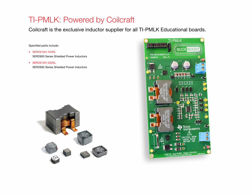
TI-PMLK: Powered by CoilcraftCoilcraft is the exclusive inductor supplier for all TI-PMLK Educational boards.
Specified parts include:
• SER2915H-103KL
SER2900 Series Shielded Power Inductors
• SER2915H-332KL
SER2900 Series Shielded Power Inductors

79 | TI Power Management Lab Kit Texas Instruments
Coilcraft understands that inductors can be difficult for students to understand, so we’re committed to upporting you with the same tools and resources professional engineers rely on when designing power management and analog circuits.
Coilcraft is your RF & Power Magnetic resourceFree product samples
Need some Coilcraft parts for your design project? We’ll ship them today.
Application notes
Our App Notes and Design Guides cover topics you might not learn about in class.
Industry’s best design tools
Our powerful on-line tools will lead you to the perfect part quickly and easily.
Free Power Management Lab Kit
This free parts tool kit helps instructors bring practical experience into the classroom.
Learn more @ Coilcraft.com/students

IMPORTANT NOTICE
TI Power Management Lab Kit (“TI-PMLK”) – Buck-Boost Experiment Book is intended to introduce students to basic electronic theory and circuits through experiments outlined in this book. While Texas Instruments Incorporated and its subsidiaries (TI) update information periodically, it may not be current at the time you conduct experiments set forth in the book. You understand and agree that you remain responsible for using your independent analysis, evaluation and judgment in conducting experiments contemplated by this book. In addition to the terms below, your use of this book is subject to TI’s Terms of Use located at http://www.ti.com/corp/docs/legal/termsofuse.shtml which are incorporated herein by this reference.
THE MATERIAL CONTAINED IN THIS BOOK (THE “CONTENT”) IS PROVIDED “AS IS”. TI MAKES NO WARRANTIES OR REPRESENTATIONS WITH REGARD TO THIS CONTENT, OR USE OF THIS CONTENT, WHETHER EXPRESS, IMPLIED, OR STATUTORY, INCLUDING ACCURACY OR COMPLETENESS. TI DISCLAIMS ANY WARRANTY OF TITLE AND ANY IMPLIED WARRANTIES OF MERCHANTABILITY, FITNESS FOR A PARTICULAR PURPOSE, QUIET ENJOYMENT, QUIET POSSESSION, AND NON-INFRINGEMENT OF ANY THIRD PARTY INTELLECTUAL PROPERTY RIGHTS WITH REGARD TO THE CONTENT OR THE USE OF THE CONTENT. TI SHALL NOT BE LIABLE FOR ANY ACTUAL, SPECIAL, INCIDENTAL, CONSEQUENTIAL OR INDIRECT DAMAGES, HOWEVER CAUSED, ON ANY THEORY OF LIABILITY AND WHETHER OR NOT TI HAS BEEN ADVISED OF THE POSSIBILITY OF SUCH DAMAGES, ARISING IN ANY WAY OUT OF THE CONTENT OR USE OF THE CONTENT.
Certain books may contain experiments which contemplate the use of materials obtained from third parties and/or other materials that may be linked at www.ti.com. IN ALL SUCH INSTANCES, TI OFFERS NO WARRANTIES (EITHER EXPRESS OR IMPLIED), INDEMNIFICATION, OR SUPPORT OF ANY KIND WITH RESPECT TO THIRD PARTY MATERIALS AND, TO THE EXTENT PERMITTED BY LAW, ALL DISCLAIMERS OF WARRANTIES AND LIMITATIONS OF LIABILITY WITHIN THIS NOTICE WILL APPLY TO THE THIRD PARTY MATERIALS, AS WELL.

81 | TI Power Management Lab Kit Texas Instruments
STANDARD TERMS AND CONDITIONS FOR EVALUATION MODULES
1. Delivery: TI delivers TI evaluation boards, kits, or modules, including any accompanying demonstration software, components, or documentation (collectively, an “EVM” or “EVMs”) to the User (“User”) in accordance with the terms and conditions set forth herein. Acceptance of the EVM is expressly subject to the following terms and conditions.1.1 EVMs are intended solely for product or software developers for use in a research and development setting to facilitate feasibility evaluation, experimentation, or scientific analysis of TI semiconduc-
tors products. EVMs have no direct function and are not finished products. EVMs shall not be directly or indirectly assembled as a part or subassembly in any finished product. For clarification, any software or software tools provided with the EVM (“Software”) shall not be subject to the terms and conditions set forth herein but rather shall be subject to the applicable terms and conditions that accompany such Software
1.2 EVMs are not intended for consumer or household use. EVMs may not be sold, sublicensed, leased, rented, loaned, assigned, or otherwise distributed for commercial purposes by Users, in whole or in part, or used in any finished product or production system.
2. Limited Warranty and Related Remedies/Disclaimers:2.1 These terms and conditions do not apply to Software. The warranty, if any, for Software is covered in the applicable Software License Agreement.2.2 TI warrants that the TI EVM will conform to TI’s published specifications for ninety (90) days after the date TI delivers such EVM to User. Notwithstanding the foregoing, TI shall not be liable for any
defects that are caused by neglect, misuse or mistreatment by an entity other than TI, including improper installation or testing, or for any EVMs that have been altered or modified in any way by an entity other than TI. Moreover, TI shall not be liable for any defects that result from User’s design, specifications or instructions for such EVMs. Testing and other quality control techniques are used to the extent TI deems necessary or as mandated by government requirements. TI does not test all parameters of each EVM.
2.3 If any EVM fails to conform to the warranty set forth above, TI’s sole liability shall be at its option to repair or replace such EVM, or credit User’s account for such EVM. TI’s liability under this warranty shall be limited to EVMs that are returned during the warranty period to the address designated by TI and that are determined by TI not to conform to such warranty. If TI elects to repair or replace such EVM, TI shall have a reasonable time to repair such EVM or provide replacements. Repaired EVMs shall be warranted for the remainder of the original warranty period. Replaced EVMs shall be warranted for a new full ninety (90) day warranty period.
3. Regulatory Notices:3.1 United States
3.1.1 Notice applicable to EVMs not FCC-Approved: This kit is designed to allow product developers to evaluate electronic components, circuitry, or software associated with the kit to determine whether to incorporate such items in a finished
product and software developers to write software applications for use with the end product. This kit is not a finished product and when assembled may not be resold or otherwise marketed unless all required FCC equipment authorizations are first obtained. Operation is subject to the condition that this product not cause harmful interference to licensed radio stations and that this product accept harmful interference. Unless the assembled kit is designed to operate under part 15, part 18 or part 95 of this chapter, the operator of the kit must operate under the authority of an FCC license holder or must secure an experimental authorization under part 5 of this chapter.
3.1.2 For EVMs annotated as FCC – FEDERAL COMMUNICATIONS COMMISSION Part 15 Compliant:
CAUTIONThis device complies with part 15 of the FCC Rules. Operation is subject to the following two conditions: (1) This device may not cause harmful interference, and (2) this device must accept any interference received, including interference that may cause undesired operation.
Changes or modifications not expressly approved by the party responsible for compliance could void the user’s authority to operate the equipment.
FCC Interference Statement for Class A EVM devicesNOTE: This equipment has been tested and found to comply with the limits for a Class A digital device, pursuant to part 15 of the FCC Rules. These limits are designed to provide reasonable protection against harmful interference when the equipment is operated in a commercial environment. This equipment generates, uses, and can radiate radio frequency energy and, if not installed and used in accordance with the instruction manual, may cause harmful interference to radio communications. Operation of this equipment in a residential area is likely to cause harmful interference in which case the user will be required to correct the interference at his own expense.

FCC Interference Statement for Class B EVM devicesNOTE: This equipment has been tested and found to comply with the limits for a Class B digital device, pursuant to part 15 of the FCC Rules. These limits are designed to provide reasonable protection against harmful interference in a residential installation. This equipment generates, uses and can radiate radio frequency energy and, if not installed and used in accordance with the instructions, may cause harmful interference to radio communications. However, there is no guarantee that interference will not occur in a particular installation. If this equipment does cause harmful interference to radio or television reception, which can be determined by turning the equipment off and on, the user is encouraged to try to correct the interference by one or more of the following measures:
• Reorient or relocate the receiving antenna.• ncrease the separation between the equipment and receiver.• Connect the equipment into an outlet on a circuit different from that to which the receiver is connected.• Consult the dealer or an experienced radio/TV technician for help.
3.2 Canada3.2.1 For EVMs issued with an Industry Canada Certificate of Conformance to RSS-210 Concerning EVMs Including Radio Transmitters: This device complies with Industry Canada license-exempt RSS standard(s). Operation is subject to the following two conditions: (1) this device may not cause interference, and (2) this device must
accept any interference, including interference that may cause undesired operation of the device.
Concernant les EVMs avec appareils radio: Le présent appareil est conforme aux CNR d’Industrie Canada applicables aux appareils radio exempts de licence. L’exploitation est autorisée aux deux conditions suivantes: (1) l’appareil ne doit
pas produire de brouillage, et (2) l’utilisateur de l’appareil doit accepter tout brouillage radioélectrique subi, même si le brouillage est susceptible d’en compromettre le fonctionnement.
Concerning EVMs Including Detachable Antennas: Under Industry Canada regulations, this radio transmitter may only operate using an antenna of a type and maximum (or lesser) gain approved for the transmitter by Industry Canada. To reduce
potential radio interference to other users, the antenna type and its gain should be so chosen that the equivalent isotropically radiated power (e.i.r.p.) is not more than that necessary for successful communication. This radio transmitter has been approved by Industry Canada to operate with the antenna types listed in the user guide with the maximum permissible gain and required antenna impedance for each antenna type indicated. Antenna types not included in this list, having a gain greater than the maximum gain indicated for that type, are strictly prohibited for use with this device.
Concernant les EVMs avec antennes détachables Conformément à la réglementation d’Industrie Canada, le présent émetteur radio peut fonctionner avec une antenne d’un type et d’un gain maximal (ou inférieur) approuvé pour l’émetteur par Indus-
trie Canada. Dans le but de réduire les risques de brouillage radioélectrique à l’intention des autres utilisateurs, il faut choisir le type d’antenne et son gain de sorte que la puissance isotrope rayonnée équivalente (p.i.r.e.) ne dépasse pas l’intensité nécessaire à l’établissement d’une communication satisfaisante. Le présent émetteur radio a été approuvé par Industrie Canada pour fonctionner avec les types d’antenne énumérés dans le manuel d’usage et ayant un gain admissible maximal et l’impédance requise pour chaque type d’antenne. Les types d’antenne non inclus dans cette liste, ou dont le gain est supérieur au gain maximal indiqué, sont strictement interdits pour l’exploitation de l’émetteur
3.3 Japan3.3.1 Notice for EVMs delivered in Japan: Please see http://www.tij.co.jp/lsds/ti_ja/general/eStore/notice_01.page 日本国内に輸入される評価用キット、ボードについては、次のところをご覧くださ
い。http://www.tij.co.jp/lsds/ti_ja/general/eStore/notice_01.page3.3.2 Notice for Users of EVMs Considered “Radio Frequency Products” in Japan: EVMs entering Japan may not be certified by TI as conforming to Technical Regulations of Radio Law of Japan. If User
uses EVMs in Japan, not certified to Technical Regulations of Radio Law of Japan, User is required by Radio Law ofJapan to follow the instructions below with respect to EVMs:1. Use EVMs in a shielded room or any other test facility as defined in the notification #173 issued by Ministry of Internal Affairs and Communications on March 28, 2006, based on Sub-section 1.1 of
Article 6 of the Ministry’s Rule for Enforcement of Radio Law of Japan,2. Use EVMs only after User obtains the license of Test Radio Station as provided in Radio Law of Japan with respect to EVMs, or3. Use of EVMs only after User obtains the Technical Regulations Conformity Certification as provided in Radio Law of Japan with respect to EVMs. Also, do not transfer EVMs, unless User gives the same
notice above to the transferee. Please note that if User does not follow the instructions above, User will be subject to penalties of Radio Law of Japan.

83 | TI Power Management Lab Kit Texas Instruments
【無線電波を送信する製品の開発キットをお使いになる際の注意事項】開発キットの中には技術基準適合証明を受けていないものがあります。技術適合証明を受けていないもののご使用に際しては、電波法遵守のため、以下のいずれかの措置を取っていただく必要がありますのでご注意ください。
1. 電波法施行規則第6条第1項第1号に基づく平成18年3月28日総務省告示第173号で定められた電波暗室等の試験設備でご使用いただく。2. 実験局の免許を取得後ご使用いただく。3. 技術基準適合証明を取得後ご使用いただく。なお、本製品は、上記の「ご使用にあたっての注意」を譲渡先、移転先に通知しない限り、譲渡、移転できないものとします。上記を遵守頂け
ない場合は、電波法の罰則が適用される可能性があることをご留意ください。日本テキサス・インスツルメンツ株式会社東京都新宿区西新宿6丁目24番1号西新宿三井ビル
3.3.3 Notice for EVMs for Power Line Communication: Please see http://www.tij.co.jp/lsds/ti_ja/general/eStore/notice_02.page 電力線搬送波通信についての開発キットをお使いになる際の注意事項については、次のところをご覧ください。 http://www.tij.co.jp/lsds/ti_ja/general/eStore/notice_02.page
4. EVM Use Restrictions and Warnings:4.1 EVMS ARE NOT FOR USE IN FUNCTIONAL SAFETY AND/OR SAFETY CRITICAL EVALUATIONS, INCLUDING BUT NOT LIMITED TO EVALUATIONS OF LIFE SUPPORT APPLICATIONS.4.2 User must read and apply the user guide and other available documentation provided by TI regarding the EVM prior to handling or using the EVM, including without limitation any warning or restriction
notices. The notices contain important safety information related to, for example, temperatures and voltages.4.3 Safety-Related Warnings and Restrictions:
4.3.1 User shall operate the EVM within TI’s recommended specifications and environmental considerations stated in the user guide, other available documentation provided by TI, and any other applicable requirements and employ reasonable and customary safeguards. Exceeding the specified performance ratings and specifications (including but not limited to input and output voltage, current, power, and environmental ranges) for the EVM may cause personal injury or death, or property damage. If there are questions concerning performance ratings and specifications, User should contact a TI field representative prior to connecting interface electronics including input power and intended loads. Any loads applied outside of the specified output range may also result in unintended and/or inaccurate operation and/or possible permanent damage to the EVM and/or interface electronics. Please consult the EVM user guide prior to connecting any load to the EVM output. If there is uncertainty as to the load specification, please contact a TI field representative. During normal operation, even with the inputs and outputs kept within the specified allowable ranges, some circuit components may have elevated case temperatures. These components include but are not limited to linear regulators, switching transistors, pass transistors, current sense resistors, and heat sinks, which can be identified using the information in the associated documentation. When working with the EVM, please be aware that the EVM may become very warm.
4.3.2 EVMs are intended solely for use by technically qualified, professional electronics experts who are familiar with the dangers and application risks associated with handling electrical mechanical components, systems, and subsystems. User assumes all responsibility and liability for proper and safe handling and use of the EVM by User or its employees, affiliates, contractors or designees. User assumes all responsibility and liability to ensure that any interfaces (electronic and/or mechanical) between the EVM and any human body are designed with suitable isolation and means to safely limit accessible leakage currents to minimize the risk of electrical shock hazard. User assumes all responsibility and liability for any improper or unsafe handling or use of the EVM by User or its employees, affiliates, contractors or designees.
4.4 User assumes all responsibility and liability to determine whether the EVM is subject to any applicable international, federal, state, or local laws and regulations related to User’s handling and use of the EVM and, if applicable, User assumes all responsibility and liability for compliance in all respects with such laws and regulations. User assumes all responsibility and liability for proper disposal and recycling of the EVM consistent with all applicable international, federal, state, and local requirements.
5. Accuracy of Information: To the extent TI provides information on the availability and function of EVMs, TI attempts to be as accurate as possible. However, TI does not warrant the accuracy of EVM descriptions, EVM availability or other information on its websites as accurate, complete, reliable, current, or error-free.

6. Disclaimers:6.1 EXCEPT AS SET FORTH ABOVE, EVMS AND ANY WRITTEN DESIGN MATERIALS PROVIDED WITH THE EVM (AND THE DESIGN OF THE EVM ITSELF) ARE PROVIDED “AS IS” AND “WITH ALL
FAULTS.” TI DISCLAIMS ALL OTHER WARRANTIES, EXPRESS OR IMPLIED, REGARDING SUCH ITEMS, INCLUDING BUT NOT LIMITED TO ANY IMPLIED WARRANTIES OF MERCHANTABILITY OR FITNESS FOR A PARTICULAR PURPOSE OR NON-INFRINGEMENT OF ANY THIRD PARTY PATENTS, COPYRIGHTS, TRADE SECRETS OR OTHER INTELLECTUAL PROPERTY RIGHTS.
6.2 EXCEPT FOR THE LIMITED RIGHT TO USE THE EVM SET FORTH HEREIN, NOTHING IN THESE TERMS AND CONDITIONS SHALL BE CONSTRUED AS GRANTING OR CONFERRING ANY RIGHTS BY LICENSE, PATENT, OR ANY OTHER INDUSTRIAL OR INTELLECTUAL PROPERTY RIGHT OF TI, ITS SUPPLIERS/LICENSORS OR ANY OTHER THIRD PARTY, TO USE THE EVM IN ANY FINISHED END-USER OR READY-TO-USE FINAL PRODUCT, OR FOR ANY INVENTION, DISCOVERY OR IMPROVEMENT MADE, CONCEIVED OR ACQUIRED PRIOR TO OR AFTER DELIVERY OF THE EVM.
7. USER’S INDEMNITY OBLIGATIONS AND REPRESENTATIONS. USER WILL DEFEND, INDEMNIFY AND HOLD TI, ITS LICENSORS AND THEIR REPRESENTATIVES HARMLESS FROM AND AGAINST ANY AND ALL CLAIMS, DAMAGES, LOSSES, EXPENSES, COSTS AND LIABILITIES (COLLECTIVELY, “CLAIMS”) ARISING OUT OF OR IN CONNECTION WITH ANY HANDLING OR USE OF THE EVM THAT IS NOT IN ACCORDANCE WITH THESE TERMS AND CONDITIONS. THIS OBLIGATION SHALL APPLY WHETHER CLAIMS ARISE UNDER STATUTE, REGULATION, OR THE LAW OF TORT, CONTRACT OR ANY OTHER LEGAL THEORY, AND EVEN IF THE EVM FAILS TO PERFORM AS DESCRIBED OR EXPECTED.
8. Limitations on Damages and Liability:8.1 General Limitations. IN NO EVENT SHALL TI BE LIABLE FOR ANY SPECIAL, COLLATERAL, INDIRECT, PUNITIVE, INCIDENTAL, CONSEQUENTIAL, OR EXEMPLARY DAMAGES IN CONNECTION
WITH OR ARISING OUT OF THESE TERMS ANDCONDITIONS OR THE USE OF THE EVMS PROVIDED HEREUNDER, REGARDLESS OF WHETHER TI HAS BEEN ADVISED OF THE POSSIBILIT OF SUCH DAMAGES. EXCLUDED DAMAGES INCLUDE, BUT ARE NOT LIMITED TO, COST OF REMOVAL OR REINSTALLATION, ANCILLARY COSTS TO THE PROCUREMENT OF SUBSTITUTE GOODS OR SERVICES, RETESTING, OUTSIDE COMPUTER TIME, LABOR COSTS, LOSS OF GOODWILL, LOSS OF PROFITS, LOSS OF SAVINGS, LOSS OF USE, LOSS OF DATA, OR BUSINESS INTERRUPTION. NO CLAIM, SUIT OR ACTION SHALL BE BROUGHT AGAINST TI MORE THAN ONE YEAR AFTER THE RELATED CAUSE OF ACTION HAS OCCURRED.
8.2 Specific Limitations. IN NO EVENT SHALL TI’S AGGREGATE LIABILITY FROM ANY WARRANTY OR OTHER OBLIGATION ARISING OUT OF OR IN CONNECTION WITH THESE TERMS AND CONDITIONS, OR ANY USE OF ANY TI EVM PROVIDED HEREUNDER, EXCEED THE TOTAL AMOUNT PAID TO TI FOR THE PARTICULAR UNITS SOLD UNDER THESE TERMS AND CONDITIONS WITH RESPECT TO WHICH LOSSES OR DAMAGES ARE CLAIMED. THE EXISTENCE OF MORE THAN ONE CLAIM AGAINST THE PARTICULAR UNITS SOLD TO USER UNDER THESE TERMS AND CONDITIONS SHALL NOT ENLARGE OR EXTEND THIS LIMIT.
9. Return Policy. Except as otherwise provided, TI does not offer any refunds, returns, or exchanges. Furthermore, no return of EVM(s) will be accepted if the package has been opened and no return of the EVM(s) will be accepted if they are damaged or otherwise not in a resalable condition. If User feels it has been incorrectly charged for the EVM(s) it ordered or that delivery violates the applicable order, User should contact TI. All refunds will be made in full within thirty (30) working days from the return of the components(s), excluding any postage or packaging costs.
10. Governing Law: These terms and conditions shall be governed by and interpreted in accordance with the laws of the State of Texas, without reference to conflict-of-laws principles. User agrees that non-exclusive jurisdiction for any dispute arising out of or relating to these terms and conditions lies within courts located in the State of Texas and consents to venue in Dallas County, Texas. Notwithstanding the foregoing, any judgment may be enforced in any United States or foreign court, and TI may seek injunctive relief in any United States or foreign court.
Mailing Address: Texas Instruments, Post Office Box 655303, Dallas, Texas 75265Copyright © 2016, Texas Instruments Incorporated

85 | TI Power Management Lab Kit Texas Instruments

The platform bar is a trademark of Texas Instruments. © 2016 Texas Instruments Incorporated. SSQU009A
PMLK BUCKBOOSTEVM Rev A
TI-PMLKTI Power Management Lab KitBuck-Boost Experiment Book

IMPORTANT NOTICE FOR TI DESIGN INFORMATION AND RESOURCES
Texas Instruments Incorporated (‘TI”) technical, application or other design advice, services or information, including, but not limited to,reference designs and materials relating to evaluation modules, (collectively, “TI Resources”) are intended to assist designers who aredeveloping applications that incorporate TI products; by downloading, accessing or using any particular TI Resource in any way, you(individually or, if you are acting on behalf of a company, your company) agree to use it solely for this purpose and subject to the terms ofthis Notice.TI’s provision of TI Resources does not expand or otherwise alter TI’s applicable published warranties or warranty disclaimers for TIproducts, and no additional obligations or liabilities arise from TI providing such TI Resources. TI reserves the right to make corrections,enhancements, improvements and other changes to its TI Resources.You understand and agree that you remain responsible for using your independent analysis, evaluation and judgment in designing yourapplications and that you have full and exclusive responsibility to assure the safety of your applications and compliance of your applications(and of all TI products used in or for your applications) with all applicable regulations, laws and other applicable requirements. Yourepresent that, with respect to your applications, you have all the necessary expertise to create and implement safeguards that (1)anticipate dangerous consequences of failures, (2) monitor failures and their consequences, and (3) lessen the likelihood of failures thatmight cause harm and take appropriate actions. You agree that prior to using or distributing any applications that include TI products, youwill thoroughly test such applications and the functionality of such TI products as used in such applications. TI has not conducted anytesting other than that specifically described in the published documentation for a particular TI Resource.You are authorized to use, copy and modify any individual TI Resource only in connection with the development of applications that includethe TI product(s) identified in such TI Resource. NO OTHER LICENSE, EXPRESS OR IMPLIED, BY ESTOPPEL OR OTHERWISE TOANY OTHER TI INTELLECTUAL PROPERTY RIGHT, AND NO LICENSE TO ANY TECHNOLOGY OR INTELLECTUAL PROPERTYRIGHT OF TI OR ANY THIRD PARTY IS GRANTED HEREIN, including but not limited to any patent right, copyright, mask work right, orother intellectual property right relating to any combination, machine, or process in which TI products or services are used. Informationregarding or referencing third-party products or services does not constitute a license to use such products or services, or a warranty orendorsement thereof. Use of TI Resources may require a license from a third party under the patents or other intellectual property of thethird party, or a license from TI under the patents or other intellectual property of TI.TI RESOURCES ARE PROVIDED “AS IS” AND WITH ALL FAULTS. TI DISCLAIMS ALL OTHER WARRANTIES ORREPRESENTATIONS, EXPRESS OR IMPLIED, REGARDING TI RESOURCES OR USE THEREOF, INCLUDING BUT NOT LIMITED TOACCURACY OR COMPLETENESS, TITLE, ANY EPIDEMIC FAILURE WARRANTY AND ANY IMPLIED WARRANTIES OFMERCHANTABILITY, FITNESS FOR A PARTICULAR PURPOSE, AND NON-INFRINGEMENT OF ANY THIRD PARTY INTELLECTUALPROPERTY RIGHTS.TI SHALL NOT BE LIABLE FOR AND SHALL NOT DEFEND OR INDEMNIFY YOU AGAINST ANY CLAIM, INCLUDING BUT NOTLIMITED TO ANY INFRINGEMENT CLAIM THAT RELATES TO OR IS BASED ON ANY COMBINATION OF PRODUCTS EVEN IFDESCRIBED IN TI RESOURCES OR OTHERWISE. IN NO EVENT SHALL TI BE LIABLE FOR ANY ACTUAL, DIRECT, SPECIAL,COLLATERAL, INDIRECT, PUNITIVE, INCIDENTAL, CONSEQUENTIAL OR EXEMPLARY DAMAGES IN CONNECTION WITH ORARISING OUT OF TI RESOURCES OR USE THEREOF, AND REGARDLESS OF WHETHER TI HAS BEEN ADVISED OF THEPOSSIBILITY OF SUCH DAMAGES.You agree to fully indemnify TI and its representatives against any damages, costs, losses, and/or liabilities arising out of your non-compliance with the terms and provisions of this Notice.This Notice applies to TI Resources. Additional terms apply to the use and purchase of certain types of materials, TI products and services.These include; without limitation, TI’s standard terms for semiconductor products http://www.ti.com/sc/docs/stdterms.htm), evaluationmodules, and samples (http://www.ti.com/sc/docs/sampterms.htm).
Mailing Address: Texas Instruments, Post Office Box 655303, Dallas, Texas 75265Copyright © 2018, Texas Instruments Incorporated