Plastic deformation mechanisms in nanocrystalline columnar …€¦ · Plastic deformation...
18
Plastic deformation mechanisms in nanocrystalline columnar grain structures Diana Farkas a and William A. Curtin b a Department of Materials Science and Engineering, Virginia Tech, Blacksburg, VA 24061, USA b Division of Engineering, Brown University, Providence, RI 02912, USA Elsevier use only: Received date here; revised date here; accepted date here Abstract We present an atomistic study of the plastic deformation mechanisms occurring in columnar structures of nanocrystalline Ni. The samples are constructed with grain boundaries characterized by random tilt misorientations around a common <110> type axis. All samples contain the same 36 grain polycrystalline microstructure, with grain sizes ranging from 4 to 20 nm in order to isolate size effects on the deformation mechanisms. Tensile deformations up to 8% were simulated and the strain stress curves observed for these samples show grain size effects in both the elastic and plastic portions. An inverse Hall-Petch effect is observed for the nominal stress at a fixed strain, but disappears when the grain-size-dependent elastic modulus is used to construct an 0.5% offset yield stress. Both dislocation emission from the grain boundaries and grain boundary accommodation of plasticity are observed. Dislocation emission comes largely from pre-existing dislocation-like structures in the grain boundaries, and increases rapidly for grain sizes > 4 nm. However, the number of dislocations per unit length of grain boundary saturates to a constant value at large grain sizes, indicating a fixed density pre-existing sources in the grain boundaries. A simple model wherein dislocation emission is prohibited within a small distance from grain triple junctions accounts for the overall density versus grain size. Grain boundary sliding was observed in the same regions of the microstructure in all grain sizes, and to approximately the same degree. A simple model accounting for both dislocations and sliding is consistent with the observed trends in plastic strain versus grain size. The implications of these observations for more realistic three dimensional samples are briefly discussed. © 2001 Elsevier Science. All rights reserved Kewords: Dislocations, grain boundaries, deformation. PACS: Type your PACS codes here, separated by semicolons ;
Transcript of Plastic deformation mechanisms in nanocrystalline columnar …€¦ · Plastic deformation...
Plastic deformation mechanisms in nanocrystalline columnar grain structures
Diana Farkasa and William A. Curtinb aDepartment of Materials Science and Engineering, Virginia Tech, Blacksburg, VA 24061, USA
bDivision of Engineering, Brown University, Providence, RI 02912, USA
Elsevier use only: Received date here; revised date here; accepted date here
Abstract
We present an atomistic study of the plastic deformation mechanisms occurring in columnar structures of nanocrystalline Ni. The samples are constructed with grain boundaries characterized by random tilt misorientations around a common <110> type axis. All samples contain the same 36 grain polycrystalline microstructure, with grain sizes ranging from 4 to 20 nm in order to isolate size effects on the deformation mechanisms. Tensile deformations up to 8% were simulated and the strain stress curves observed for these samples show grain size effects in both the elastic and plastic portions. An inverse Hall-Petch effect is observed for the nominal stress at a fixed strain, but disappears when the grain-size-dependent elastic modulus is used to construct an 0.5% offset yield stress. Both dislocation emission from the grain boundaries and grain boundary accommodation of plasticity are observed. Dislocation emission comes largely from pre-existing dislocation-like structures in the grain boundaries, and increases rapidly for grain sizes > 4 nm. However, the number of dislocations per unit length of grain boundary saturates to a constant value at large grain sizes, indicating a fixed density pre-existing sources in the grain boundaries. A simple model wherein dislocation emission is prohibited within a small distance from grain triple junctions accounts for the overall density versus grain size. Grain boundary sliding was observed in the same regions of the microstructure in all grain sizes, and to approximately the same degree. A simple model accounting for both dislocations and sliding is consistent with the observed trends in plastic strain versus grain size. The implications of these observations for more realistic three dimensional samples are briefly discussed. © 2001 Elsevier Science. All rights reserved
Kewords: Dislocations, grain boundaries, deformation. PACS: Type your PACS codes here, separated by semicolons ;
Submitted to Elsevier Science 2
1. Introduction The mechanical behavior of nanocrystalline materials has been the subject of extensive research in recent years. The main observation prompting these studies is the dramatically increased yield strength due to the Hall–Petch relation [1]. However, below a critical grain size, the conventional dislocation slip mechanism does not operate and the yield stresses decrease with decreasing grain size, as shown by several simulation studies [2-4]. Computer simulation in general provides a level of detail regarding the deformation mechanisms operating in metallic materials that is not attainable using experimental techniques [5]. In previous work by several investigators fully three dimensional finite temperature molecular dynamics calculations have been performed for grain sizes up to 40 nm. Generally, these data show a crossover in deformation mechanism from dislocation mechanisms at larger grain sizes to grain boundary deformation mechanisms at smaller grain sizes [2,4]. There are several rationalizations of this crossover that take into account various ways in which the grain size can influence the relative importance of these two mechanisms, ranging from assumptions that dislocation emission is easier from grain boundaries in the case of larger grain sizes [6] to the fact that grain boundary sliding can be easier at smaller grain sizes, with a grain size dependence of 1/d [7]. The crossover has also been linked to the length scale of dislocation splitting [3]. The details of the processes of grain boundary sliding are not well understood and there is no quantitative measure of the ease of dislocation emission from grain boundaries or the sliding process. Van Swygenhoven et al [8] have proposed that the grain boundary re-accommodates after the emission of dislocations and that the process occurs through the migration of free volume. The details of the dislocation emission process are very difficult to grasp in 3D samples, as is the process of grain boundary sliding. Detailed simulations can be performed in the columnar grain geometry in reasonable computing times for relatively large grain sizes. In addition, the columnar grain structure makes visualization much easier and analysis of the various mechanisms of plastic deformation is possible without the complications of the fully 3D configuration. Although the columnar grain structure introduces specific constraints to the overall deformation behavior of the sample, it does yield information on how grain size can affect the various deformation mechanisms. In particular, in order to understand the behavior of nanocrystalline materials in general it is important to understand how very small grain sizes affect the plastic deformation processes of dislocation emission/ propagation and grain boundary sliding. The purpose of the present work is to use the simple geometry of columnar crystals in order to study aspects of the dislocation emission process and the grain boundary sliding process, and their corresponding effects on the stress strain curves. We apply molecular statics [9] to study samples with many (36) grains in a columnar structure with common <110> axis and a constant microstructure to investigate a reasonable statistical distribution of grains and boundaries and a systematic analysis of changes with grain size with no other changes in the simulations. We find increasing dislocation activity with increasing grain size, but with the dislocations per unit grain boundary length saturating at large grain sizes. We also observe grain boundary sliding at all grain sizes, largely independent of the grain size. We relate these observations to features of the measured stress-strain curves through a simple model that qualitatively accounts for the observed plastic strains and predicts an inverse-Hall-Petch regime at small grain sizes.
2. Methodology
The initial atomic configurations are generated using a Voronoi construction, as described in detail in previous simulations [2]. The columnar grains in the sample are generating by using a common [110] axis for all grains and a random rotation angle around this axis for the various grains. The samples contained 36 grains with average grain sizes of 4 to 20 nm. Periodicity is maintained in all directions. The periodicity
Submitted to Elsevier Science 3
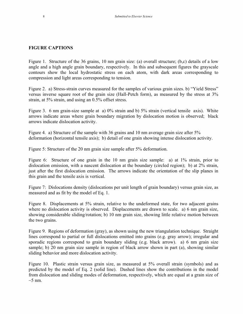
along the [110] axis common to all grains is kept at the lattice periodicity along that direction. The resulting samples contain up to about one quarter million atoms, for grain sizes of 20 nm. The present simulations utilize an EAM potential for Ni that is based on first principle calculations [9]. The potential was developed to reproduce not only many equilibrium lattice and defect properties of fcc Ni, but also the predictions of ab-initio LAPW calculations for metastable phases for Ni. The latter calculations span a wide range of configurations far from equilibrium and the transferability of this potential to situations very far from equilibrium is therefore very good. This is an important consideration for large plastic deformation simulations, since regions such as dislocation cores can be in configurations that are very different from equilibrium lattice situations. After their initial creation, the samples were fully relaxed using a conjugate gradient technique, including simultaneous energy minimization with respect to the total sample volume. The grain boundaries present in samples generated in this manner have been fully characterized in previous work [11]. A large degree of structural coherence is observed across most of the grain boundaries present, in spite of the fact that the orientations of each grain and grain boundary location are the result of random selection. The samples of different grain sizes and the same number of grains were constructed with the same misorientations and grain boundary planes to facilitate comparison and isolate particular effect of the grain size. The grain boundary structures themselves are independent of grain size and it is only the extent of grain boundary material that is different in the samples with different grain sizes. As shown in our previous work there is no tendency for amorphization in the boundary region. The relaxed configuration is used as a starting configuration in the molecular statics technique to study the response to an applied strain that mimics uniaxial loading. For the visualization of dislocations we primarily use the local stress tensor (multiplied by the atomic volume) calculated at each atom, which also provides information on the overall state of stress of the sample corresponding to the imposed strain. We use contour plots of the hydrostatic stress to show the location of the grain boundaries and the dislocations that are emitted in the plastic regime, with dark areas representing compression and light areas representing tension. Figure 1a shows the overall structure of the sample containing 36 grains of 10 nm average diameter. Figures 1b and 1c show detail of a low angle and a high angle grain boundary respectively, with atomic symbols corresponding to the positions of the atoms projected onto the {110} plane also shown. Note that this visualization technique allows for the clear identification of the individual dislocations that compose the low angle grain boundary. The presence of dislocations as seen by the grayscale plotting of local stress states can be confirmed by various Burgers circuits in the detailed Figures 1b and 1c. To visualize both dislocations and inelastic grain boundary deformations, we use a new superimposed triangulation technique as follows. The un-deformed structure is first triangulated via the Delaunay method in two dimensions, which creates a connectivity matrix of near-neighbor atoms in the initial reference state. In any deformed structure, a second triangulation is then performed. The connectivity matrix of the un-deformed structure is then used to create a third triangulation of the deformed structure and the two (second and third) triangulations are compared. Differences between them show only those deformations connecting pairs of atoms that were neighbors in the original structure but are no longer neighbors in the deformed structure. The relative orientation of these atom pairs shows the nature of the deformation, whether shear, extension, or a combination of the two. This visualization scheme thus clearly exposes stacking faults, the passage of full dislocations, the locations of dislocation cores, and any inelastic grain boundary deformations that arise, as we shall show below.
Submitted to Elsevier Science 4
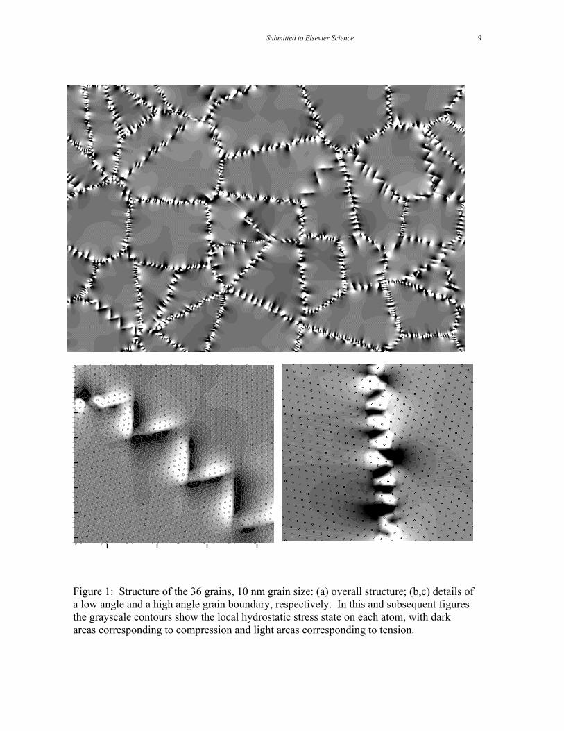
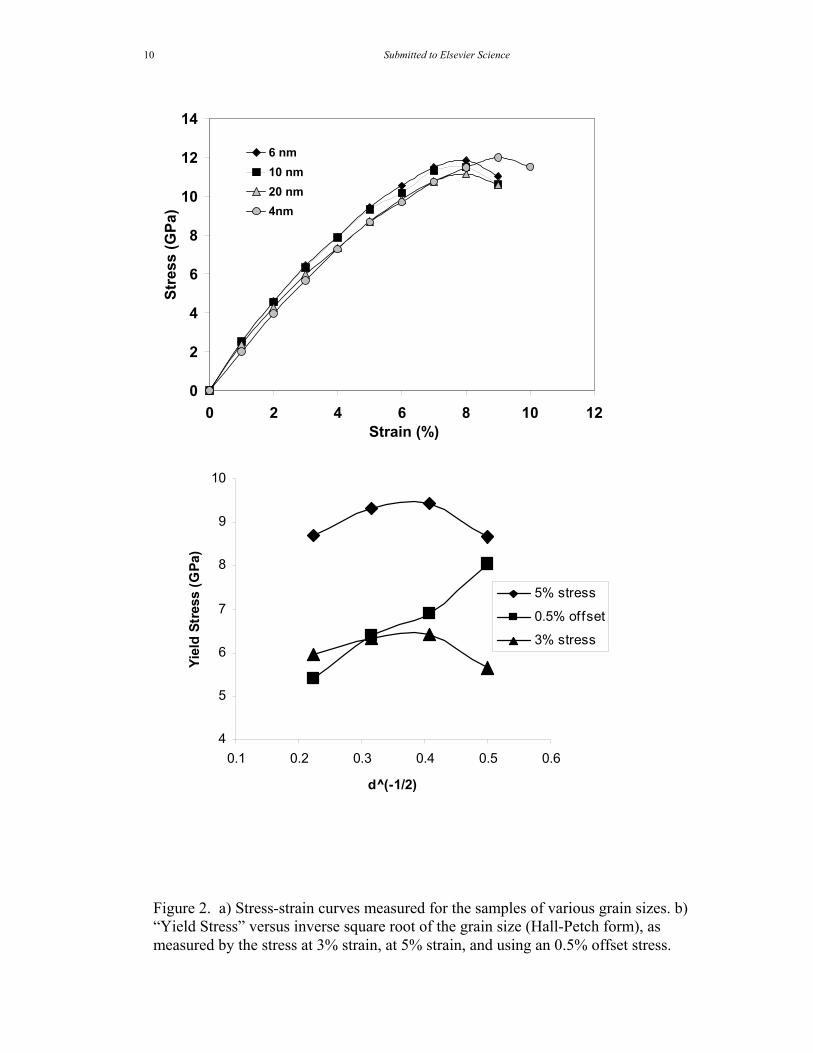
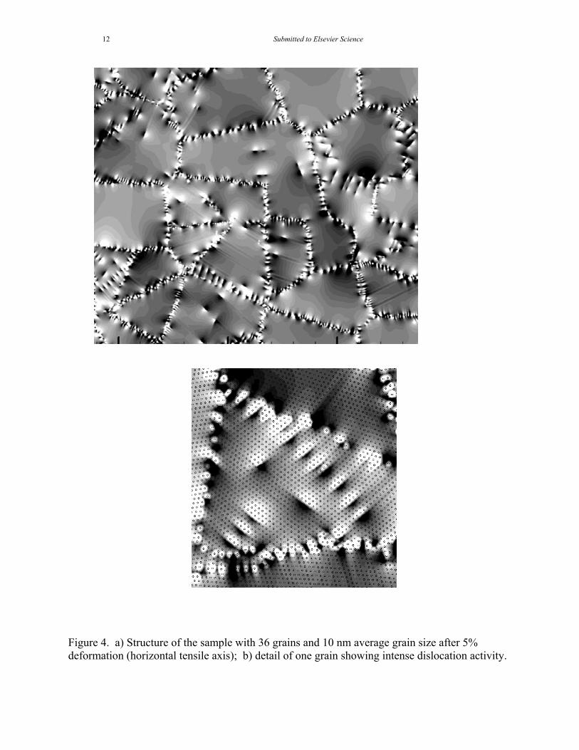
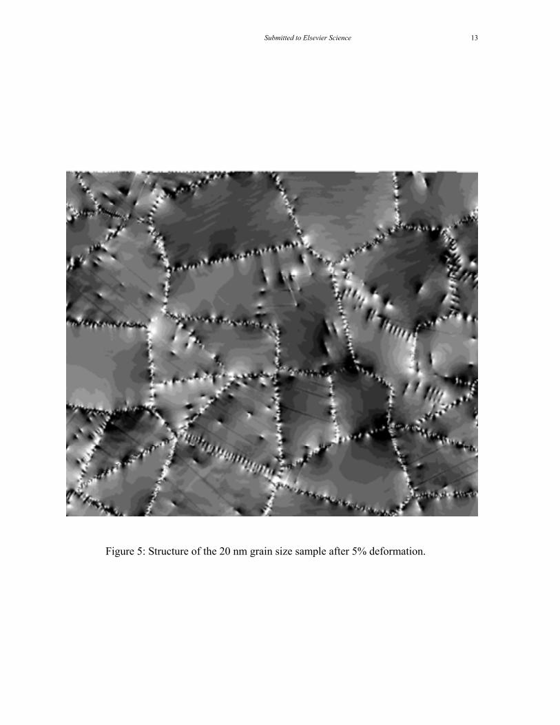
3. Results and discussion Figure 2a shows the stress-strain behavior observed for the columnar nanocrystalline samples studied. The elastic part of this curve yields values of the elastic modulus ranging from 201 GPa for the 4 nm grain size sample and ~250 GPa for the samples with grain sizes of 6 nm and above. The yield stresses observed are high due to restrictions in dislocation nucleation at the boundaries imposed by the columnar structure of the sample and to the lack of dislocation sources within the grains. The plastic deformation can be attributed to both dislocation processes and grain boundary accommodation mechanisms, as we shall show. Figure 2b shows the average stress of the samples at 3% and 5% strain as a function of grain size. In agreement with previous observations, the stress shows a maximum between 6 and 10 nm. However, this maximum is due to the elastic softening observed in the 4 nm sample. An 0.5% offset yield stress, also shown in Figure 2b, demonstrates that the 4 nm sample has a higher offset yield stress, indicating less plastic deformation for the smaller grain size material. To study the plastic deformation mechanisms, we analyzed the structure of the strained samples using the local stress state to visualize the deformation. Figure 3 shows the sample with 36 grains of 6 nm average size at a strain of 5%, together with the initial structure for comparison. The tensile axis is vertical. In Figure 3, we can observe the motion of low angle boundaries, indicated by white arrows. We also observe the emission of Shockley partial dislocations from grain boundaries traveling across a grain to a nearby grain boundary where they are absorbed, as indicated by the black arrows. Figure 4a shows the sample with 10nm average grains deformed at 5% strain, which can be compared with the undeformed sample shown in Figure 1a. The phenomena are similar to those seen for 6 nm grains (Figure 3) but with a larger number of dislocations emitted, some of which remain within the interiors of the grains. Some grains show no dislocation emission at all and some show intense dislocation activity. Figure 4b shows a detail of one grain in the lower portion of the sample that presents intense dislocation activity. Figure 5 shows the dislocation activity present in the 20 nm sample at 5% strain, indicating that dislocation activity increases dramatically with grain size. We have investigated some features of the dislocation emission from the grain boundaries. Figure 6a shows the structure of the same grain shown in figure 4b at 1% deformation, just before the dislocation emission process in this grain begins. Figure 6b shows the structure of the same region at 2% deformation, just after the first partial was emitted from the grain boundary into this grain. This grain is oriented such that both slip planes are close to the 45% maximum shear stress directions for vertical tensile loading. This particular grain is triangular in shape and the grain boundaries that constitute the top sides emit dislocations whereas the bottom side of the grain is a grain boundary that does not emit dislocations into this grain. Considering the grain boundaries as modeled by dislocation walls, we note that the top grain boundary actually contains in its structure a series of dislocations with cores spread along planes belonging to one of the two slip planes in this grain. Dislocation emission corresponds to the motion of one of these “pre-existing” dislocations when the stress reaches a critical resolved value. Other dislocations remain as a part of the grain boundary structure after emission (Figure 6b). The important point here is that dislocation emission from the grain boundaries is often initiated in areas that can be characterized as containing a pre-existing dislocation, and after emission there is subsequent re-accommodation of the grain boundary structure. This is contrary to the view that the boundary contains dislocation sources that are not modified by the process of emission. The process of dislocation emission is also shown to be strongly dependent on the particular details of each individual grain boundary (misorientation across the boundary, and orientation relative to the loading axis). We have performed a quantitative analysis of the dislocation density as a function of grain size. This was done by counting the total number of dislocations emitted at the 5% strain level. Tthere are no sources inside the grains and all the dislocations observed originate at the grain boundaries, and so we calculate a dislocation density ρ as the number of dislocations emitted per unit length (in two dimensions) of grain
Submitted to Elsevier Science 5
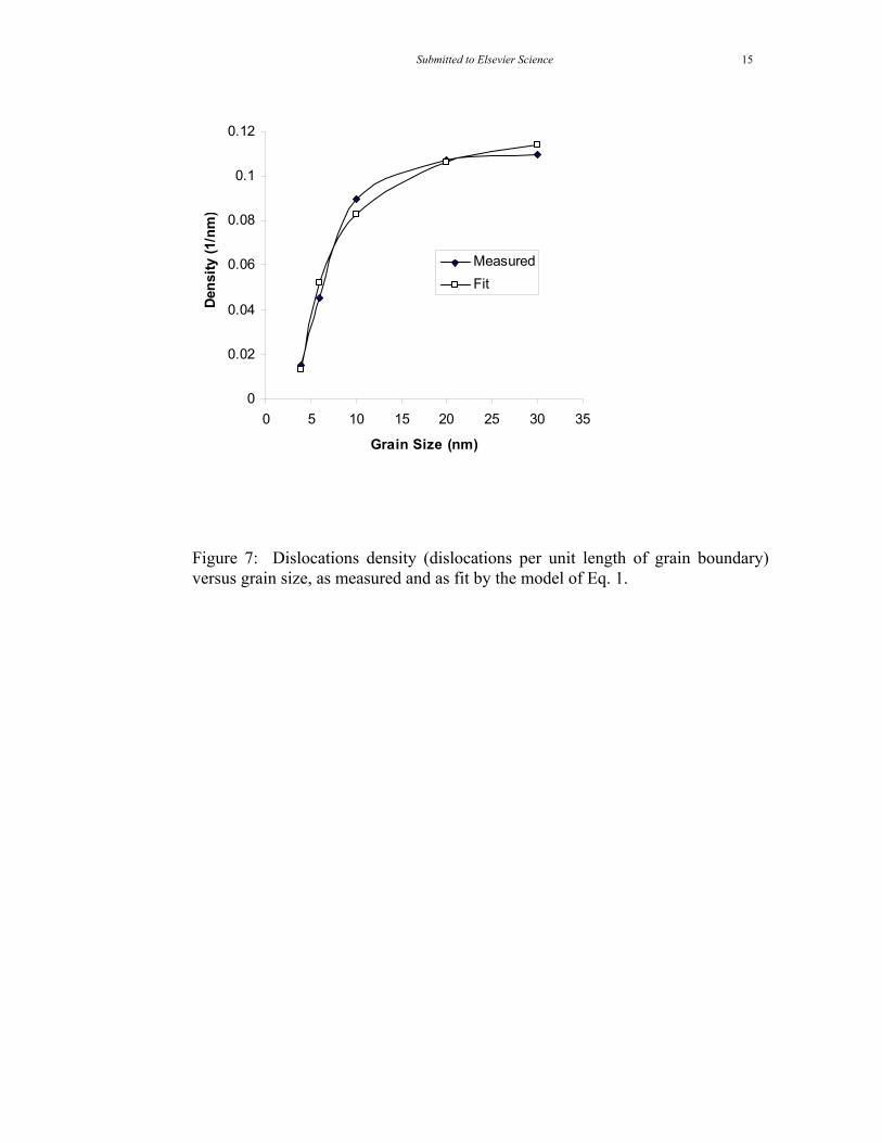
boundary. Since the grain boundaries have identical structures for the samples of different grain sizes, we can quantify the effect of grain size on the dislocation density. Figure 7 shows that the dislocation density increases rapidly beyond a critical grain size and then approaches a saturation value satρ for grain sizes approaching 30 nm (the 30 nm data is obtained on a 16-grain sample, however). This result indicates that any given grain boundary having a specific orientation with respect to the loading axis contains a constant density, per unit length, of “sources”. Although some grain boundaries emit many more dislocations than others, each has its own particular capacity for dislocation emission. However, at sufficiently small grain sizes, here below about 10 nm, the grain boundaries cannot produce the same density of dislocations. One rationalization for the reduction is that the triple junctions effectively pin any nearby nascent or “pre-existing” boundary dislocations. This suggests the following simple model: each grain boundary has a region of length D near each triple junction that is prohibited from emitting dislocations so that the dislocation density per unit grain boundary length scales as
)/1( dDsat −= ρρ . (1)
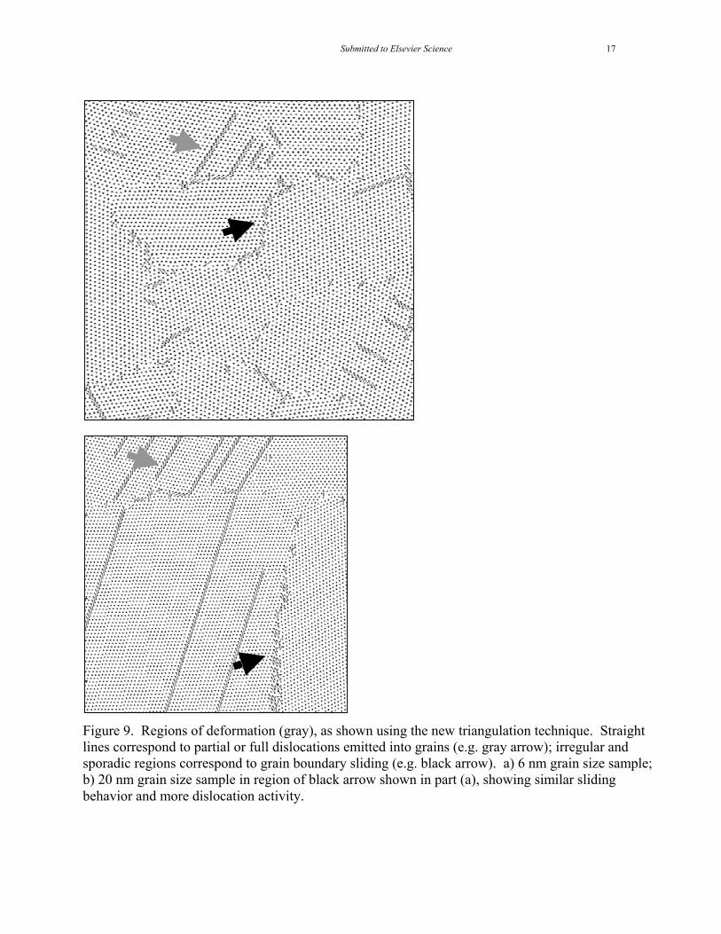
The data in Figure 7 is reasonably fit using D=1.8 nm and nmsat /13.0=ρ , as shown in the figure. Since the dislocation density decreases so dramatically at small grain sizes and yet the yield stress does not increase correspondingly fast, we have investigated the possibility of other deformation mechanisms. In particular, we have assessed the relative importance of grain boundary sliding versus grain size. Figures 8a,b show the relative displacement of two grains that do not show dislocation activity in either 6 or 10 nm grain sizes at the 5% strain level. The results indicate significant grain boundary sliding in the 6 nm sample that is not present in the 10 nm sample. Nonetheless, the stress-strain curves of the two grain sizes are very similar. Since the 10 nm sample exhibits increased overall dislocation activity, a transition in deformation mechanism from grain rotation/sliding to dislocation plasticity is suggested with increasing grain size. To show the presence of both types of plastic deformation mechanisms more distinctly, we used the new triangulation approach. Figure 9a shows this analysis for the 6 nm grain size sample. Partial dislocations are observed as straight regions of differing triangulation; one such dislocation is indicated by the gray arrow. Grain sliding, in the form of disordered shearing along sections of grain boundaries, is also observed; one such case is indicated by the black arrow. Figure 9b shows the same grain boundary region in the 20 nm grain size sample as indicated by the black arrow in Figure 9a, and again sliding is clearly evident and to the same degree. In other words, for some boundaries, the absolute magnitude of the sliding at the same strain is independent of grain size. This idea is supported by many similar cases across the range of samples studied here.
As an aside, the sporadic and more-localized regions of grain boundary deformation are observed on other boundaries in the portion of the structure shown in Figures 9. Although the sporadic deformations do not extend along the length of the grain boundaries, the deformation can contribute to the plastic deformation in a manner analogous to the plasticity of localized shear domains in amorphous systems [12].
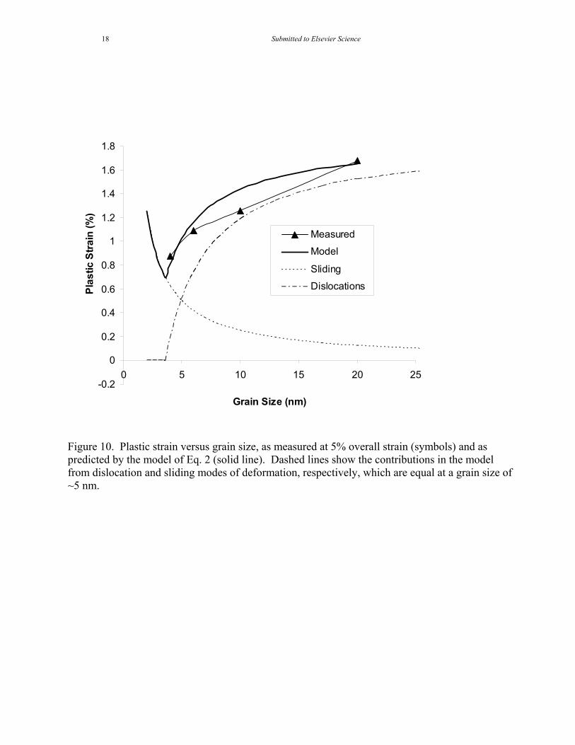
We can combine the measured dislocation density with the occurrence of grain boundary sliding into a simple model for the plastic strain in the deforming crystal. The contribution to the plastic strain from dislocation emission is simply bρ , where b is the Burger’s vector for the observed partial dislocations. The plastic strain due to grain boundary sliding is obtained by considering each grain boundary as analogous to an additional single slip plane in the material that can accommodate a “Burger’s vector” of some magnitude sb to the deformation. Since not all grain boundaries can slide, and we have no measure of the fraction of sliding boundaries, we introduce a fraction f of sliding boundaries. The total plastic strain due to the grain boundary sliding then depends on grain size, since the absolute number of grain boundaries does not change with grain size. Hence, the total plastic strain due to both dislocations and sliding is modeled as
Submitted to Elsevier Science 6
dfbspl /=ε Dd <
dfbdDb ssatpl /)/1( +−= ρε Dd > . (2) Treating the dimensionless combination bfbs / as a single adjustable parameter, we fit the measure plastic strain (total strain minus elastic contribution) using the measured dislocation density at 5% strain. For the value bfbs / =0.175, we obtain the predicted plastic strain as shown in Figure 10; the simulation data at 5% total strain or ~9 GPa applied stress is also shown. In general, the plastic strain decreases with decreasing grain size until dislocation plasticity ceases below 3.6 nm, after which the remaining sliding deformation predicts an increase in plastic strain. The qualitative agreement obtained here is encouraging, given the simplicity of the model. We have not investigated smaller grain sizes in any attempt to check the increasing plastic strain component, however. 4. Discussion and Summary
We have examined the deformation of columnar-grained nanocrystalline materials under quasistatic loading and zero temperature, where nucleation of defects is most difficult and strain rate effects are largely absent. We have observed grain-boundary-dominated deformation mechanisms of dislocation emission from the boundary and grain-boundary sliding. The dislocation emission stems from “pre-existing” dislocations in the boundaries. For large grain sizes, the density of such dislocations, at least at one strain of 5%, becomes independent of grain size. The finite number of dislocations able to be activated at a particular applied load suggests that these “sources” are exhausted after only one dislocation is emitted. A simple model accounting for the dislocation density data suggests that dislocation emission is difficult near triple junctions, but is not otherwise easier for larger grain sizes as postulated in Ref. 6. We also observe, via a new visualization technique, grain boundary “sliding” behavior, even though the simulations are carried out at zero temperature. The sliding that occurs appears in the same structural region largely independent of grain size, suggesting that this motion is also due to pre-existing grain-boundary structures that are susceptible to sliding deformation in the same manner as other grain boundaries are susceptible to dislocation emission into the grains. Thus, grain boundary sliding is not easier at smaller grain sizes, in contrast to the postulate put forth in Ref. 7. However, the contribution of sliding to the overall plastic strain does scale with 1/d for geometric reasons, as suggested in Ref. 7. A simple model that combines both sliding and dislocation deformation is able to quantitatively account for the dependence of the plastic strain versus grain size observed in the simulations. Although grain sliding is predicted to dominate for sizes less than 5 nm, it is notable that, over the range of sizes from 4-20 nm in this system, the plastic strain increases with increasing grain size, so that smaller sizes are harder; i.e. there is no inverse Hall-Petch effect under these conditions in this size range. The inverse Hall-Petch effect may thus be a temperature-dependent phenomenon governed by the relative competing rates of the dislocation emission and grain-boundary sliding phenomena that control the deformation. Consistent with this view is the fact that the inverse Hall-Petch effect is typically observed under flow conditions and is not usually obtained by a standard offset yield stress measurement on from a stress-strain curve as done here. Otherwise, these columnar grain samples demonstrate the range of phenomena exhibited in fully three dimensional samples, but permit the investigation of much larger grain sizes and with constant microstructure. In future work, we will report on observations of failure phenomena, such as void nucleation and growth, and crack propagation, as well as the deformation under nanoindentation loading conditions, to uncover other effects of the competing deformation modes and grain size in this class of nanomaterials.
Submitted to Elsevier Science 7
Acknowledgements: The authors acknowledge support from the US AFOSR through grant #F49620-99-1-0272 under the MURI program “Virtual Design and Testing of Materials: A Multiscale Approach” at Brown University, and from the General Motors/Brown Collaborative Research Laboratory on Computational Materials. References
[1] Kumar, KS; Van Swygenhoven, H; Suresh, S, Acta Materialia, 51 (19): 5743-5774 (2003) [2] Van Swygenhoven, H; Spaczer, M; Caro, A; Farkas, D, Physical Review B, 60 (1): 22-25
(1999) [3] Yamakov, V; Wolf, D; Phillpot, SR; Mukherjee, AK; Gleiter, H, Nature Materials, 1 45-
48 (2002) [4] Schiotz, J; Jacobsen, KW, Science, 301 (5638): 1357-1359 (2003) [5] Li, J; Ngan, AHW; Gumbsch, P, Acta Materialia, 51 (19): 5711-5742 (2003) [6] Van Vliet, KJ; Tsikata, S; Suresh, S, Applied Physics Letters, 83 (7): 1441-1443 (2003) [7] Van Swygenhoven, H; Caro, A, Physical Review B, 58 (17): 11246-11251 (1998) [8] Van Swygenhoven, H; Derlet, PM; Hasnaoui, A, Physical Review B, 66, 024101 (2002) [9] Farkas, D; Van Swygenhoven, H; Derlet, PM, Physical Review B, 66, 060101(2002) [10] Y. Mishin, D. Farkas, M.J. Mehl and D. Papaconstantopoulos, Physical Review B, Vol. 59
(5), 3393-3407 (1999) [11] Van Swygenhoven, H; Farkas, D; Caro, A, Physical Review B, 62 (2): 831-838 (2000) [12] Fu,XY, Rigney DA, Falk, ML, Journal Of Non-Crystalline Solids 317 206-214 (2003)
Submitted to Elsevier Science 8
FIGURE CAPTIONS Figure 1. Structure of the 36 grains, 10 nm grain size: (a) overall structure; (b,c) details of a low angle and a high angle grain boundary, respectively. In this and subsequent figures the grayscale contours show the local hydrostatic stress on each atom, with dark areas corresponding to compression and light areas corresponding to tension. Figure 2. a) Stress-strain curves measured for the samples of various grain sizes. b) “Yield Stress” versus inverse square root of the grain size (Hall-Petch form), as measured by the stress at 3% strain, at 5% strain, and using an 0.5% offset stress. Figure 3. 6 nm grain-size sample at a) 0% strain and b) 5% strain (vertical tensile axis). White arrows indicate areas where grain boundary migration by dislocation motion is observed; black arrows indicate dislocation activity. Figure 4. a) Structure of the sample with 36 grains and 10 nm average grain size after 5% deformation (horizontal tensile axis); b) detail of one grain showing intense dislocation activity. Figure 5: Structure of the 20 nm grain size sample after 5% deformation. Figure 6: Structure of one grain in the 10 nm grain size sample: a) at 1% strain, prior to dislocation emission, with a nascent dislocation at the boundary (circled region); b) at 2% strain, just after the first dislocation emission. The arrows indicate the orientation of the slip planes in this grain and the tensile axis is vertical. Figure 7: Dislocations density (dislocations per unit length of grain boundary) versus grain size, as measured and as fit by the model of Eq. 1. Figure 8. Displacements at 5% strain, relative to the undeformed state, for two adjacent grains where no dislocation activity is observed. Displacements are drawn to scale. a) 6 nm grain size, showing considerable sliding/rotation; b) 10 nm grain size, showing little relative motion between the two grains. Figure 9. Regions of deformation (gray), as shown using the new triangulation technique. Straight lines correspond to partial or full dislocations emitted into grains (e.g. gray arrow); irregular and sporadic regions correspond to grain boundary sliding (e.g. black arrow). a) 6 nm grain size sample; b) 20 nm grain size sample in region of black arrow shown in part (a), showing similar sliding behavior and more dislocation activity. Figure 10. Plastic strain versus grain size, as measured at 5% overall strain (symbols) and as predicted by the model of Eq. 2 (solid line). Dashed lines show the contributions in the model from dislocation and sliding modes of deformation, respectively, which are equal at a grain size of ~5 nm.
Submitted to Elsevier Science 9
Figure 1: Structure of the 36 grains, 10 nm grain size: (a) overall structure; (b,c) details of a low angle and a high angle grain boundary, respectively. In this and subsequent figures the grayscale contours show the local hydrostatic stress state on each atom, with dark areas corresponding to compression and light areas corresponding to tension.
Submitted to Elsevier Science 10
0
2
4
6
8
10
12
14
0 2 4 6 8 10 12 Strain (%)
Stre
ss (G
Pa)
6 nm 10 nm20 nm 4nm
4
5
6
7
8
9
10
0.1 0.2 0.3 0.4 0.5 0.6
d^(-1/2)
Yiel
d St
ress
(GPa
)
5% stress
0.5% offset
3% stress
Figure 2. a) Stress-strain curves measured for the samples of various grain sizes. b) “Yield Stress” versus inverse square root of the grain size (Hall-Petch form), as measured by the stress at 3% strain, at 5% strain, and using an 0.5% offset stress.
Submitted to Elsevier Science 11
Figure 3. 6 nm grain-size sample at a) 0% strain and b) 5% strain (vertical tensile
axis). White arrows indicate areas where grain boundary migration by dislocation motion is observed; black arrows indicate dislocation activity.
Submitted to Elsevier Science 12
Figure 4. a) Structure of the sample with 36 grains and 10 nm average grain size after 5% deformation (horizontal tensile axis); b) detail of one grain showing intense dislocation activity.
Submitted to Elsevier Science 13
Figure 5: Structure of the 20 nm grain size sample after 5% deformation.

Submitted to Elsevier Science 14
a) b)
Figure 6: Structure of one grain in the 10 nm grain size sample: a) at 1% strain, prior to dislocation emission, with a nascent dislocation at the boundary (circled region); b) at 2% strain, just after the first dislocation emission. The arrows indicate the orientation of the slip planes in this grain and the tensile axis is vertical.
Submitted to Elsevier Science 15
0
0.02
0.04
0.06
0.08
0.1
0.12
0 5 10 15 20 25 30 35
Grain Size (nm)
Den
sity
(1/n
m)
MeasuredFit
Figure 7: Dislocations density (dislocations per unit length of grain boundary)versus grain size, as measured and as fit by the model of Eq. 1.

Submitted to Elsevier Science 16
a) b)
Figure 8. Displacements at 5% strain, relative to the undeformed state, for two adjacent grains where no dislocation activity is observed. Displacements are drawn to scale. a) 6 nm grain size, showing considerable sliding/rotation; b) 10 nm grain size, showing little relative motion between the two grains.
Submitted to Elsevier Science 17
Figure 9. Regions of deformation (gray), as shown using the new triangulation technique. Straight lines correspond to partial or full dislocations emitted into grains (e.g. gray arrow); irregular and sporadic regions correspond to grain boundary sliding (e.g. black arrow). a) 6 nm grain size sample; b) 20 nm grain size sample in region of black arrow shown in part (a), showing similar sliding behavior and more dislocation activity.
Submitted to Elsevier Science 18
-0.2
0
0.2
0.4
0.6
0.8
1
1.2
1.4
1.6
1.8
0 5 10 15 20 25
Grain Size (nm)
Plas
tic S
train
(%)
Measured
Model
Sliding
Dislocations
Figure 10. Plastic strain versus grain size, as measured at 5% overall strain (symbols) and as predicted by the model of Eq. 2 (solid line). Dashed lines show the contributions in the model from dislocation and sliding modes of deformation, respectively, which are equal at a grain size of ~5 nm.