Plasmonics of topological insulators at optical frequencies · OPEN ORIGINAL ARTICLE Plasmonics of...
8
OPEN ORIGINAL ARTICLE Plasmonics of topological insulators at optical frequencies Jun Yin 1 , Harish NS Krishnamoorthy 2 , Giorgio Adamo 2 , Alexander M Dubrovkin 2 , Yidong Chong 1,2 , Nikolay I Zheludev 1,2,3 and Cesare Soci 1,2 The development of nanoplasmonic devices, such as plasmonic circuits and metamaterial superlenses in the visible to ultraviolet frequency range, is hampered by the lack of low-loss plasmonic media. Recently, strong plasmonic response was reported in a certain class of topological insulators. Here, we present a first-principles density functional theory analysis of the dielectric functions of topologically insulating quaternary (Bi,Sb) 2 (Te,Se) 3 trichalcogenide compounds. Bulk plasmonic properties, dominated by interband transitions, are observed from 2 to 3 eV and extend to higher frequencies. Moreover, trichalcogenide compounds are better plasmonic media than gold and silver at blue and UV wavelengths. By analyzing thin slabs, we also show that these materials exhibit topologically protected surface states, which are capable of supporting propagating plasmon polariton modes over an extremely broad spectral range, from the visible to the mid-infrared and beyond, owing to a combination of inter- and intra-surface band transitions. NPG Asia Materials (2017) 9, e425; doi:10.1038/am.2017.149; published online 25 August 2017 INTRODUCTION The fields of metamaterials and plasmonics have seen an extraordinary evolution in recent years, from the initial theoretical predictions of artificial negative refractive indices and cloaking 1,2 to the experimental realization of photonic metadevices with various functionalities that can be engineered and obtained on demand. 3,4 However, the practical implementations of plasmonic and metamaterial devices have long been hampered by energy dissipation in plasmonic media, especially in the visible to ultraviolet (UV) range, where even the best plasmonic metals (such as gold, silver and aluminum) suffer from strong dissipation due to interband electronic transitions and Drude losses. 5 This has inspired a search for alternative low-loss plasmonic materials for optical devices operating at high frequencies. 6,7 Candidates that are currently being investigated include highly doped semiconductors, metallic alloys, nitrides and oxides 8 and, more recently, two- dimensional materials and topological insulator (TI) materials. TIs represent a new quantum phase of matter, which originates from the topological character of the bulk electronic bands in certain materials. The strong spin–orbit coupling in such materials leads to a band inversion and the appearance of Dirac surface states in the band gap. These topological surface states are chiral and protected from back-scattering by time-reversal symmetry. As a consequence, charge carriers from topologically protected surface states can carry current and are free to move parallel to the surface. Thus, TIs are ideal candidates to realize exotic plasmonic phenomena. Localized plasmons have recently been observed in TIs at THz frequencies (in Bi 2 Se 3 ) 9,10 as well as visible-to-UV frequencies (in single crystal Bi 1.5 Sb 0.5 Te 1.8 Se 1.2 , or BSTS). 11 These experiments observed large bulk resistances and surface-dominated transport. 12,13 In addition, multiple plasmon modes were recently reported in solution-synthesized Bi 2 Te 3 nanoplates 14 and nano-discs and flakes of BSTS. 15 Ellipsometric data indicated the presence of high optical conductivities, possibly linked to the existence of topologically protected surface states. If true, BSTS or other TIs would be a radically new material platform for broadband nanoplasmonic devices that can be modulated optically, 16 through injection of electrons, 17 or by applied magnetic fields. 18 In this work, we use density functional theory (DFT) calculations to investigate the electronic band structures and optical properties of seven compounds in the Bi x Sb 1-x Te y Se 1-y (BSTS) family of TIs, in bulk crystal and thin film forms, with the overall goal of determining their suitability for nanoplasmonics (similar ab-initio studies have proven effective with metals, 19–21 alkali-noble intermetallics 22 and gallium- doped zinc oxide 23 ). Our results show that plasmonic behavior of quaternary trichalcogenide compounds in the optical part of the spectrum has three origins: (a) bulk interband transitions contributing primarily in the visible spectral region; (b) intraband transition within topologically protected surface bands contributing in the mid-infrared region; (c) interband transition between topologically protected sur- face states and bulk states, dominating in the UV–near-infrared (NIR) range. MATERIALS AND METHODS DFT calculations were used to study the electronic structure and optical response of TI materials employing the local-density approximation, using the 1 Division of Physics and Applied Physics, School of Physical and Mathematical Sciences, Nanyang Technological University, Singapore, Singapore; 2 Centre for Disruptive Photonic Technologies, TPI, Nanyang Technological University, Singapore, Singapore and 3 Optoelectronics Research Centre, University of Southampton, Southampton, UK Correspondence: Dr C Soci, Centre for Disruptive Photonic Technologies, Nanyang Technological University, 21 Nanyang Link, Singapore 637371, Singapore. E-mail: [email protected] Received 17 February 2017; revised 3 June 2017; accepted 21 June 2017 NPG Asia Materials (2017) 9, e425; doi:10.1038/am.2017.149 www.nature.com/am
Transcript of Plasmonics of topological insulators at optical frequencies · OPEN ORIGINAL ARTICLE Plasmonics of...

OPEN
ORIGINAL ARTICLE
Plasmonics of topological insulators at opticalfrequencies
Jun Yin1, Harish NS Krishnamoorthy2, Giorgio Adamo2, Alexander M Dubrovkin2, Yidong Chong1,2,Nikolay I Zheludev1,2,3 and Cesare Soci1,2
The development of nanoplasmonic devices, such as plasmonic circuits and metamaterial superlenses in the visible to ultraviolet
frequency range, is hampered by the lack of low-loss plasmonic media. Recently, strong plasmonic response was reported in a
certain class of topological insulators. Here, we present a first-principles density functional theory analysis of the dielectric
functions of topologically insulating quaternary (Bi,Sb)2(Te,Se)3 trichalcogenide compounds. Bulk plasmonic properties,
dominated by interband transitions, are observed from 2 to 3 eV and extend to higher frequencies. Moreover, trichalcogenide
compounds are better plasmonic media than gold and silver at blue and UV wavelengths. By analyzing thin slabs, we also show
that these materials exhibit topologically protected surface states, which are capable of supporting propagating plasmon polariton
modes over an extremely broad spectral range, from the visible to the mid-infrared and beyond, owing to a combination of inter-
and intra-surface band transitions.
NPG Asia Materials (2017) 9, e425; doi:10.1038/am.2017.149; published online 25 August 2017
INTRODUCTION
The fields of metamaterials and plasmonics have seen an extraordinaryevolution in recent years, from the initial theoretical predictions ofartificial negative refractive indices and cloaking1,2 to the experimentalrealization of photonic metadevices with various functionalities thatcan be engineered and obtained on demand.3,4 However, the practicalimplementations of plasmonic and metamaterial devices have longbeen hampered by energy dissipation in plasmonic media, especially inthe visible to ultraviolet (UV) range, where even the best plasmonicmetals (such as gold, silver and aluminum) suffer from strongdissipation due to interband electronic transitions and Drude losses.5
This has inspired a search for alternative low-loss plasmonic materialsfor optical devices operating at high frequencies.6,7 Candidates that arecurrently being investigated include highly doped semiconductors,metallic alloys, nitrides and oxides8 and, more recently, two-dimensional materials and topological insulator (TI) materials.TIs represent a new quantum phase of matter, which originates
from the topological character of the bulk electronic bands in certainmaterials. The strong spin–orbit coupling in such materials leads to aband inversion and the appearance of Dirac surface states in the bandgap. These topological surface states are chiral and protected fromback-scattering by time-reversal symmetry. As a consequence, chargecarriers from topologically protected surface states can carry currentand are free to move parallel to the surface. Thus, TIs are idealcandidates to realize exotic plasmonic phenomena. Localized plasmonshave recently been observed in TIs at THz frequencies (in Bi2Se3)
9,10
as well as visible-to-UV frequencies (in single crystal
Bi1.5Sb0.5Te1.8Se1.2, or BSTS).11 These experiments observed large bulk
resistances and surface-dominated transport.12,13 In addition, multipleplasmon modes were recently reported in solution-synthesized Bi2Te3nanoplates14 and nano-discs and flakes of BSTS.15 Ellipsometric dataindicated the presence of high optical conductivities, possibly linked tothe existence of topologically protected surface states. If true, BSTS orother TIs would be a radically new material platform for broadbandnanoplasmonic devices that can be modulated optically,16 throughinjection of electrons,17 or by applied magnetic fields.18
In this work, we use density functional theory (DFT) calculations toinvestigate the electronic band structures and optical properties ofseven compounds in the BixSb1-xTeySe1-y (BSTS) family of TIs, in bulkcrystal and thin film forms, with the overall goal of determining theirsuitability for nanoplasmonics (similar ab-initio studies have proveneffective with metals,19–21 alkali-noble intermetallics22 and gallium-doped zinc oxide23). Our results show that plasmonic behavior ofquaternary trichalcogenide compounds in the optical part of thespectrum has three origins: (a) bulk interband transitions contributingprimarily in the visible spectral region; (b) intraband transition withintopologically protected surface bands contributing in the mid-infraredregion; (c) interband transition between topologically protected sur-face states and bulk states, dominating in the UV–near-infrared(NIR) range.
MATERIALS AND METHODSDFT calculations were used to study the electronic structure and opticalresponse of TI materials employing the local-density approximation, using the
1Division of Physics and Applied Physics, School of Physical and Mathematical Sciences, Nanyang Technological University, Singapore, Singapore; 2Centre for Disruptive PhotonicTechnologies, TPI, Nanyang Technological University, Singapore, Singapore and 3Optoelectronics Research Centre, University of Southampton, Southampton, UKCorrespondence: Dr C Soci, Centre for Disruptive Photonic Technologies, Nanyang Technological University, 21 Nanyang Link, Singapore 637371, Singapore.E-mail: [email protected] 17 February 2017; revised 3 June 2017; accepted 21 June 2017
NPG Asia Materials (2017) 9, e425; doi:10.1038/am.2017.149www.nature.com/am
Quantum ESPRESSO code.24 Experimental lattice parameters of bulk TImaterials12,25 were used as the initial structure, and ground states geometriesof the TI systems were obtained by the total energy minimization method uponrelaxing their crystal framework and atomic coordinates. Electron-ion interac-tions (plane waves and core electrons) were generated by norm-conservingnon-relativistic and relativistic pseudopotentials with electrons for Bi (6s2, 6p3,5d10); Sb (5s2, 5p3); Se (4s2, 4p2); and Te (5s2, 5p2, 4d10). The relativisticeffects and spin–orbital coupling (SOC) have significant effects on the bandstructure due to heavy elements, such as Bi, Sb and Te. Supplementary Figure 1shows the small energy differences (o0.005 Ry) between all-electron and ourgenerated pseudopotentials, confirming the good transferability properties ofthese pseudopotentials. Single-particle wavefunctions (charges) were expandedon a plane-wave basis set up to a kinetic energy cutoff of 80 Ry (500 Ry) forboth TI bulk and slabs. The bulk and thin film layers were relaxed until forceson the atoms were lower than 0.01 eV/Å. The k-space grid of 6× 6×6 in theBrillouin zone was chosen for the calculation of the band structures.The optical response calculations were performed by the Bethe-Salpeter
equations (BSE) method with the YAMBO code, using ground state wavefunc-tions from Quantum ESPRESSO:26,27
Eck � Evkð ÞASvck þ
Xk0v0c0
/vck Kehj jv0c0k0SASv0c0k0 ¼ OSAS
vck
where Eck and Evk are the quasiparticle energies of the conduction and valencestates, respectively; AS
vck are the expansion coefficients of the excitons, and ΩS
are the eigenenergies.The imaginary part of the permittivity was calculated by evaluating direct
electronic transitions between occupied and higher-energy unoccupied electro-nic states as obtained from
ε0 oð ÞpXS
Xcvk
ASvck
ckjpijvkEck � Evk
�����
�����d OS � _o� G� �
where ckjpijvk� �
are the dipole matrix elements for electronic transitions fromvalence to conduction states. The real part can then be calculated via theKramers-Kronig relation ε0 oð Þ ¼ 1þ 2
pPRN0
ε00 o0ð Þo0do0
o02�o2 . SOC interactions andthe spinor wave functions were included as input for the electronic and optical
calculations on the level of many-body perturbation theory. Previously this
approach has been used to successfully study the optical properties of systems
with strong spin–orbital interaction.28 For optical permittivity calculations, a
k-point grid corresponding to 12× 12×12 and 40 conduction bands and 40
valence bands both for bulk and slabs were chosen to ensure a sufficient
description of the optical permittivity.For the crystal slabs, the optical permittivity consists of two parts: (i) the
interband contribution was calculated in the framework of the BSE method
involving transitions between two surface bands and bulk bands, as well as
transitions from surface valence band to bulk conduction bands and (ii) the
Drude-like free-electron intraband contribution from the metallic surface,
which can be described by a two-dimensional Drude model determined by the
Fermi energy, carrier scattering time and thickness of the surface layer as
described in the main text.
RESULTS AND DISCUSSION
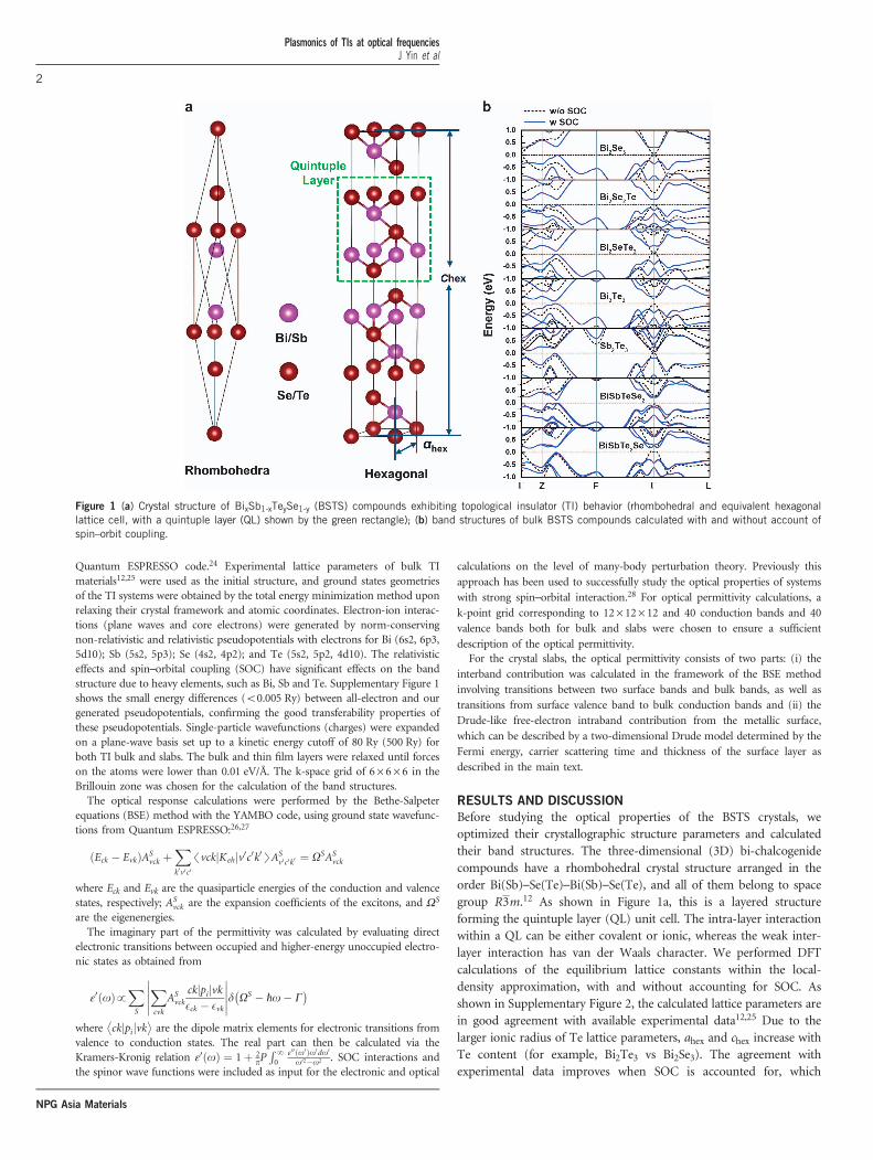
Before studying the optical properties of the BSTS crystals, weoptimized their crystallographic structure parameters and calculatedtheir band structures. The three-dimensional (3D) bi-chalcogenidecompounds have a rhombohedral crystal structure arranged in theorder Bi(Sb)–Se(Te)–Bi(Sb)–Se(Te), and all of them belong to spacegroup R3m.12 As shown in Figure 1a, this is a layered structureforming the quintuple layer (QL) unit cell. The intra-layer interactionwithin a QL can be either covalent or ionic, whereas the weak inter-layer interaction has van der Waals character. We performed DFTcalculations of the equilibrium lattice constants within the local-density approximation, with and without accounting for SOC. Asshown in Supplementary Figure 2, the calculated lattice parameters arein good agreement with available experimental data12,25 Due to thelarger ionic radius of Te lattice parameters, ahex and chex increase withTe content (for example, Bi2Te3 vs Bi2Se3). The agreement withexperimental data improves when SOC is accounted for, which
Figure 1 (a) Crystal structure of BixSb1-xTeySe1-y (BSTS) compounds exhibiting topological insulator (TI) behavior (rhombohedral and equivalent hexagonallattice cell, with a quintuple layer (QL) shown by the green rectangle); (b) band structures of bulk BSTS compounds calculated with and without account ofspin–orbit coupling.
Plasmonics of TIs at optical frequenciesJ Yin et al
2
NPG Asia Materials

indicates the validity of our chosen pseudopotentials (SupplementaryFigure 1).The calculated band structures of the seven bulk BSTS compounds
are shown in Figure 1b, both with (solid blue lines) and without (blackdashes) accounting for SOC. Without SOC, all the compounds exhibitparabolic band dispersions with small (o0.5 eV) direct band gaps atthe Γ-point. The direct gaps for the binary compounds Bi2Se3(54 meV), Bi2Te3 (159 meV) and Sb2Te3 (123 meV), as well as forthe ternary compounds Bi2Se2Te (477 meV) and Bi2Te2Se (84 meV),compare well with previous calculations.29,30 The characteristic effectof SOC on the electronic band structures of TIs is to produce a bandinversion, inducing topologically nontrivial band gaps.31,32 Such gapsare indeed observed at the Г-point for the trichalcogenide compounds(Figure 1b). The conduction band minima and valence band maximashift away from the Γ-point, along the symmetric Z-F direction,turning the direct band gaps into indirect band gaps of width0.10–0.35 eV (Supplementary Figure 3). Note that it is possible toestimate the gap energies more accurately by introducing self-energycorrections in the quasiparticle energy approximation, using many-body perturbation theory (for example, the GW method).33,34 How-ever, this would not have noticeable effects on the UV to near-infraredoptical properties, which are dominated by high-energy interbandtransitions.To quantify the plasmonic properties of BSTS compounds, we
separately evaluated their bulk and surface dielectric functions. In thebulk, the complex dielectric function (ε) originates from interbandtransitions, which we calculated from the band structures using theBethe-Salpeter and Kramers-Kronig equations (see MATERIALS ANDMETHODS). In Figure 2, we plot the real part of the dielectricfunction (ε′), which describes the strength of the polarization inducedby an external electric field, and the imaginary part (ε′′), whichdescribes the losses encountered in polarizing the material.5 Thestrongest peak in the spectral dispersion of ε′′ moves from the near-infrared
(0.5–1.5 eV) to the visible spectral region (1.5–2.5 eV) when telluriumcontent is reduced. This peak arises from interband transitionsoccurring along the symmetry line near the Γ-point (0, 0.16666,− 0.16666). Once SOC effects are included in the optical responsecalculations, we find that there are two main absorption peaks in ε′′(Supplementary Figure 5). The first peak in the visible region(1.5–2.0 eV) is red-shifted as the tellurium content is reduced, whichis attributable to the resonant character of interband transitionsbetween the spin–orbit split valence band and the lowest conductionband near the Γ valley in momentum space. As a result, the dualinterband transitions at high symmetry point around band inversionlead to the much stronger dielectric function compared to the casewithout SOC. The other strong peaks appear at ~ 0.6 eV due tointerband transitions around the (0.33333, − 0.5, − 0.5) point. Thetransition details for the optical permittivity are listed inSupplementary Table 1. The calculated values of bulk opticalpermittivity agree well with experimental data reporting prominentpeaks of the imaginary part of the permittivity between 1.5 and 2 eVfor Bi2Te3, Sb2Te3 and Bi1.5Sb0.5Te1.8Se1.2 (Figure 2b),
11,14,35 althoughcalculated permittivities at peaks are somewhat higher than theexperimentally measured ones. For the real part of the opticalpermittivity, the main features are broad peaks centered around 1.0–2.0 eV, followed by a steep decrease between 1.5 and 3.0 eV, afterwhich ε′ becomes negative and eventually increases slowly toward zeroat higher energies. The epsilon-near-zero behavior, interesting formany applications36–38 appears in the UV region, above 5 eV.Thus, for the bulk materials, plasmonic behavior emerges when ε′
becomes negative in a frequency range of around 2 eV or higher,depending on the compound. We note that negative permittivities dueto interband transitions have also been reported in previous DFTcalculations on Bi2Se3.
39 Our results show that increasing the telluriumcontent gives plasmonic behavior over a wider frequency range, withmuch larger negative values of ε′ (for example, for Bi2Te3).
Figure 2 Interband transition contribution to the real (ε′) and imaginary part (ε′′) of the permittivity of bulk BixSb1-xTeySe1-y (BSTS) materials: (a) densityfunctional theory (DFT) results without spin–orbital coupling (SOC) and (b) experimental data obtained from refs 11, 14, 35.
Plasmonics of TIs at optical frequenciesJ Yin et al
3
NPG Asia Materials

The bulk dielectric functions indicate that the BSTS compounds canoutperform plasmonic materials in the visible-to-UV spectral range,including traditional plasmonic metals. To quantify this, in Figure 3,we determine the plasmonic figure of merit,40 FOM ¼ LSPP
lSPP¼ ReðkSPPÞ
2pImðkSPPÞ,where kSPP ¼ k0
ffiffiffiffiffiffiffiffiffiffiffiεTIεairεTIþεair
qis the complex wave vector of the surface
plasmon polariton mode. Such FOM can be thought of as the numberof wavelengths a surface plasmon polariton mode can travel beforedissipation. In Figure 3 we plot the FOM of bulk BSTS compoundsobtained from our DFT calculations as well as experimental dataavailable in the literature.11,14,35 The FOM of aluminum, silver andgold are also included for comparison. Both sets of data indicate thatthe BSTS materials have higher FOM than Au below ~600 nm, andhigher FOM than Ag below ~450 nm. Most strikingly, in the UV-bluewavelengths of ~ 400 nm, surface plasmon polariton modes in bulkBSTS chalcogenide crystals are expected to propagate 3–6 wavelengthsmore than in Au or Ag. Although Al has a higher plasmonic FOMin this spectral region, its plasmonic properties are strongly dependenton the surface oxidation status.41 Note that the intrinsic electron–phonon coupling in the topological surface state of TIs is strongenough to activate the phonon-assisted intraband processes in theplasmonic response,20,42 which could slightly reduce the FOM valuesof these TIs.We now turn our attention to the surface properties of BSTS
compounds. To study the optical response of topological surfacestates, we performed DFT calculations considering thin slabs. Theemergence of topological effects and charge accumulation at surfacestates in TIs is expected to be clearly seen in slabs with thickness of afew QLs, as indicated by previous theoretical studies32,43 and experi-mental observations.44 Based on this, we carried out DFT calculationsfor a (111) crystal slab with five QLs (5QL) of approximate thicknessof ~ 5 nm, and looked for the emergence of surface states uponactivation of spin–orbital coupling. The contribution of surface statesto the optical response was then obtained considering two types oftransitions: (i) intraband transitions described by 2D Drude-like
response of surface free carriers,9,10,45 and (ii) interband transitionsfrom topological surface states to higher energy bands.Here we take Bi2Se3 slabs as an example and present their electronic
structure, charge distribution of the surface state and optical permit-tivity (Figure 4). Similar data for the other BSTS compounds areprovided in Supplementary Figures 6. Without accounting for SOCeffects, the band structure of 5QL-slab (orange solid line in Figure 4a)is similar to those of the bulk crystals obtained using periodicboundary conditions (Figure 1b). Increasing the slab thicknessdecreases the energy band gap because of the reduction in quantumconfinement, with the energy gap approaching the bulk value at about19QL thickness (Supplementary Figure 4). Upon including SOCeffects, a single non-degenerate Dirac point appears at the Γ-point.At the Dirac cone below the Fermi energy level, the electronic chargedensity distribution is mainly localized at the surface and penetrates~ 1–2 nm into the bulk (see surface layer thickness in Table 1 andintegrated charge density function in Supplementary Figure 8). Theoptical response of the 5QL Bi2Se3 slab shows similar spectral featuresas the bulk: the dominant peak of the imaginary part of thepermittivity appears at 1.6 eV, and a low-energy peak emerges around0.6 eV in agreement with the experimental dispersion curves shown inFigure 2b.Knowledge of the band structure and surface charge distribution of
the TI slabs allows extraction of other relevant parameters of the TI,such as effective mass m of the carriers, surface layer thickness d andthe surface carrier density n2D used to determine the DC conductivity,sDC2D . These parameters are listed in Table 1. For the 5QL-slabs, theeffective mass of electron was estimated by fitting the linear dispersioncurve of the lowest conduction band with the relationship m ¼ _k
vF,
where νF is the Fermi velocity,46 while total surface carrier concentra-tion was obtained by integrating the occupied surface states chargebelow Fermi energy level (the region Kʹ–Mʹ, see SupplementaryFigures 7 and 8). Note that the predicted carrier densities aresystematically higher than those derived from electrical and opticalmeasurements, since we consider all the intrinsic surface chargecarriers of TI materials, which in actual experiments could undergoseveral scattering pathways (for example, charge carrier-optical pho-non scattering or charge carrier-surface scattering). The intrabandsurface contribution to the dielectric response was determined usingthe methodology developed for other two-dimensional systems, suchas graphene.47 The DC conductivity due to the TI surface states isgiven by sDC2D ¼ 1
de2Ef tp_2
, where Ef is the Fermi energy, τ is the carrierscattering time and d is the thickness of the surface layer. At higherfrequencies, the dispersion of the optical conductivity is given by thetwo-dimensional (2D) Drude model:10,45,47,48 sAC2D ðoÞ ¼ sDC2D
ð1�iotÞ. Thecontribution of surface free carriers to the optical response can then beevaluated from the expression: ε2D oð Þ ¼ isAC2D ðoÞ
ε0o¼ i
ε0osDC2D
ð1�iotÞ. Thisexpression coincides with the dispersion of the dielectric constant ofconventional plasmonic metals, provided that the 3D static conduc-tivity, sDC3D , is replaced by the 2D static conductivity, sDC2D , of thesurface states. Unlike the case of conventional plasmonic metals,however, this dispersion relationship has no cutoff (plasma)frequency, thus yielding negative real permittivity even in theoptical spectral range, irrespectively of the carrier density (Fermienergy). The contribution of surface state intraband transitionsto the dielectric constant (Figure 5b–h, dotted lines) was quantifiedusing the parameters determined from first-principles DFT calcula-tions, except for the free carrier damping factor, assumed to beΓ= 0.07 based on the typical experimental carrier lifetime of ~ 60 fs(Table 1).49–53 The plasmonic contribution of surface free carriers israther small in the visible part of the spectrum but becomes
Figure 3 Plasmonic figures of merit for bulk BixSb1-xTeySe1-y (BSTS)compounds and noble metals determined using experimental dielectricconstants from the literature (top panel) and theoretical dielectric constantsobtained from density functional theory (DFT) calculations without spin–orbital coupling (SOC; bottom panel).
Plasmonics of TIs at optical frequenciesJ Yin et al
4
NPG Asia Materials

prominent at longer wavelengths, starting from the near IR region.This is reflected in the extremely high plasmonic figures of merit ofBSTS TI slabs at the longer wavelengths (refer to SupplementaryFigure 10a).The dielectric response arising from interband surface transitions,
that is optical transitions from topologically protected surface state tohigher energy bands, is shown in Figure 5 (solid lines). The real andimaginary part of the dielectric constants were evaluated from the DFTband structure of the TI slabs using similar methodology employed forestimating the optical response of the bulk (as described in MATERI-ALS AND METHODS). These transitions give rise to plasmonicresponse (negative real permittivity) in the optical part of the spectrumwith strong absorption features around 1.5 and 0.5 eV. In contrast tothe bulk, these surface interband transitions yield plasmonic behaviorover an extremely broad spectral range, from the visible through theNIR, with lower losses and appreciably high plasmonic figures of merit(see Supplementary Figure 10b).
Our estimate of the overall optical response arising from intra- andinter-band transitions from topological surface states of BSTS com-pounds is in good qualitative agreement with the optical permittivityof the surface of Bi1.5Sb0.5Te1.8Se1.2 determined from ellipsometricmeasurements (Figure 5a), assuming a multilayer model with a thinDrude surface layer.11 This confirms that topologically protectedsurface charge carriers have appreciable contribution to the plasmonicresponse of the TI crystals at optical frequencies, with strong Druderesponse in the infrared region and significant interband surfacecontribution throughout the optical spectrum, up to the UV. Thegood agreement with experiments gives us confidence that theproposed TI slab model, in which the contributions of the conductingsurface layer and the bulk are treated independently, can adequatelydescribe the optical and plasmonic response of this family of TImaterials. Most importantly, the cumulative plasmonic response of theTI brought about by the combination of inter- and intra-band surfacetransitions is extremely broadband in nature. Both types of transitions
Figure 4 (a) Band structure of 5QL Bi2Se3 slab without and with inclusion of spin–orbit coupling effects (the horizontal dashed line indicates the Fermienergy level and Kʹ–Mʹ the region of occupied surface states). (b) Three- and one-dimensional charge density distribution of conducting surface states; alloccupied orbitals below the Fermi level and their degeneracy (Supplementary Figure 7) were considered to calculate the average charge density.(c) Comparison between real and imaginary parts of the dielectric functions of bulk and 5QL Bi2Se3 slab with spin–orbital coupling (SOC).
Table 1 Surface state thickness s, effective mass m, two-dimensional carrier concentration n2D of surface states, carrier scattering time τ,damping factor Γ and conductivity σ of 5QL-TI slabs
Surface
Effective mass m
(×m0)
Carrier concentration
n2D(cm−2)
Fermi energy
Ef (eV)
Surface layer thick-
ness d (nm)
Carrier scattering
time τ (fs)
Damping factor
Γ=1/τ (eV)
DC conductivity
sDC2D (S/m)
Bi2Se3 DFT 0.156 6.33×10¹⁴ 0.189 0.92 — — 1.42×10⁶
Exp 0.13–0.15
(refs 49,54)
3.0±0.2×10¹³
(ref. 55)
— — 55–150
(refs 49,56)
0.028–0.075 4.54×10⁴
(ref. 57)
Bi2Se2Te DFT 0.089 2.97×10¹³ 0.171 1.27 — — 9.32×10⁵
Bi2SeTe2 DFT 0.126 7.91×10¹³ 0.259 1.28 — — 1.40×10⁶
Exp 0.11
(ref. 50)
1.50×10¹²
(ref. 43)
— — 48 (ref. 50) 0.086 1.00×10⁵
(ref. 58)
Bi2Te3 DFT 0.178 8.74×10¹³ 0.194 1.90 — — 7.07×10⁵
Exp — 7.00×10¹²
(ref. 59)
— — 54 (ref. 51) 0.077 1.65×10⁵
(ref. 60)
Sb2Te3 DFT 0.095 5.67×10¹³ 0.103 1.79 — — 3.99×10⁵
BiSbTeSe2 DFT 0.087 7.74×10¹⁴ 0.109 1.20 — — 6.29×10⁵
BiSbTe2Se DFT 0.110 9.56×10¹⁴ 0.216 2.05 — — 7.30×10⁵
Exp 0.32
(ref. 52)
3.80×10¹³
(ref. 45)
— — 58 (ref. 52) 0.071 4.57×10⁴
(ref. 61)
Abbreviations: DFT, density functional theory; QL-TI, quintuple layer–topological insulator.
Plasmonics of TIs at optical frequenciesJ Yin et al
5
NPG Asia Materials

originate from topological surface states that, besides being immune toscattering from defects, are spin-polarised and strongly coupled to thebulk. This opens up exciting opportunities for broadband plasmono-spintronic devices that can be controlled by charge injection, externalmagnetic fields, or light helicity.In summary, we presented a systematic study of the optical and
plasmonic properties of BSTS TI crystals using first-principles DFTcalculations. In addition to their negative bulk permittivity, TIs showrobust, spin-polarized surface states, which are capable of supportingsurface plasmons over a very broad wavelength range. Comparison of
the calculated dielectric functions of bulk crystals revealed thedependence of the optical band gap and permittivity on composition,indicating plasmonic behavior with figures of merit higher than noblemetals in the UV-blue spectral region. Increase of Te versus Se contentcan extend the overall plasmonic response deeper into the NIR regionand reduce losses. Furthermore, knowledge of surface charge distribu-tion in thin TI slabs has allowed isolating the plasmonic response ofthe surface. The combination of interband and intraband (2D Drude)transitions involving topologically protected surface states yieldsplasmonic response over an extremely broad spectral range. This
Figure 5 Inter- and intra-band contributions to the real and imaginary parts of the optical constants of BixSb1-xTeySe1-y (BSTS) topological insulator (TI) slabsoriginating from topological surface states. (a) Experimental values of Bi1.5Sb0.5Te1.8Se1.2 surface contribution were derived in ref. 11 using a two-layermodel. (b–h) Intraband contributions calculated according to a 2D Drude model (dotted lines) and interband contributions due to transitions from the surfacestate band to higher energy bands (solid lines).
Plasmonics of TIs at optical frequenciesJ Yin et al
6
NPG Asia Materials

new understanding of bulk and surface state contributions to theoverall plasmonic response of TIs will enable targeted strategies toexploit these materials in nanophotonic applications, for instancetailoring the growth of thin films by epitaxial growth methods tomaximize the contribution of topological surface states and lowerplasmonic losses at desired optical frequencies.
CONFLICT OF INTERESTThe authors declare no conflict of interest.
ACKNOWLEDGEMENTS
We acknowledge financial support of the Singapore Ministry of Education
(grants MOE2011-T3-1-005 and MOE2013-T2-044) and EPSRC (UK) grant
EP/M009122/1.
Author contributions: CS and JY generated the idea and designed the
simulation work. JY performed all DFT modelling. HNSK analyzed the
plasmonic response. All the authors contributed to interpretation of the results
and writing of the manuscript. CS and NIZ supervised the work.
Additional Information: Following a one year period of embargo, the data
from this paper can be obtained from the University of Southampton ePrints
research repository, https://doi.org/10.5258/SOTON/D014.
PUBLISHER’S NOTE:Springer Nature remains neutral with regard to jurisdictional claims in
published maps and institutional affiliations.
1 Smith, D. R., Pendry, J. B. & Wiltshire, M. C. K. Metamaterials and negativerefractive index. Science 305, 788–792 (2004).
2 Pendry, J. B., Schurig, D. & Smith, D. R. Controlling electromagnetic fields. Science312, 1780–1782 (2006).
3 Zheludev, N. I. & Kivshar, Y. S. From metamaterials to metadevices. Nat. Mater. 11,917–924 (2012).
4 Zheludev, N. I. Obtaining optical properties on demand. Science 348,973–974 (2015).
5 West, P. R., Ishii, S., Naik, G. V., Emani, N. K., Shalaev, V. M. & Boltasseva, A.Searching for better plasmonic materials. Laser Photonics Rev. 4, 795–808 (2010).
6 Boltasseva, A. & Atwater, H. A. Low-loss plasmonic metamaterials. Science 331,290–291 (2011).
7 Ma, X. C., Dai, Y., Yu, L. & Huang, B. B. Energy transfer in plasmonic photocatalyticcomposites. Light Sci. Appl. 5, e16017 (2016).
8 Naik, G. V., Shalaev, V. M. & Boltasseva, A. Alternative plasmonic materials: beyondgold and silver. Adv. Mater. 25, 3264–3294 (2013).
9 Di Pietro, P., Ortolani, M., Limaj, O., Di Gaspare, A., Giliberti, V., Giorgianni, F.,Brahlek, M., Bansal, N., Koirala, N., Oh, S., Calvani, P. & Lupi, S. Observation of diracplasmons in a topological insulator. Nat. Nanotechnol. 8, 556–560 (2013).
10 Autore, M., D'Apuzzo, F., Di Gaspare, A., Giliberti, V., Limaj, O., Roy, P., Brahlek, M.,Koirala, N., Oh, S., de Abajo, F. J. G. & Lupi, S. Plasmon-phonon interactions intopological insulator microrings. Adv. Opt. Mater. 3, 1257–1263 (2015).
11 Ou, J. Y., So, J. K., Adamo, G., Sulaev, A., Wang, L. & Zheludev, N. I. Ultraviolet andvisible range plasmonics in the topological insulator Bi1.5Sb0.5Te1.8Se1.2. Nat. Com-mun. 5, 5139 (2014).
12 Ren, Z., Taskin, A. A., Sasaki, S., Segawa, K. & Ando, Y. Optimizing Bi2− xSbxTe3− ySeysolid solutions to approach the intrinsic topological insulator regime. Phys. Rev. B 84,165311 (2011).
13 Yue, Z., Cai, B., Wang, L., Wang, X. & Gu, M. Intrinsically core-shell plasmonicdielectric nanostructures with ultrahigh refractive index. Sci. Adv. 2,e1501536 (2016).
14 Zhao, M., Bosman, M., Danesh, M., Zeng, M. G., Song, P., Darma, Y., Rusydi, A.,Lin, H., Qiu, C. W. & Loh, K. P. Visible surface plasmon modes in single Bi2Te3nanoplate. Nano Lett. 15, 8331–8335 (2015).
15 Dubrovkin, A. M., Adamo, G., Yin, J., Wang, L., Soci, C., Wang, Q. J. & Zheludev, N. I.Visible range plasmonic modes on topological insulator nanostructures. Adv. Opt. Mater.5, 1600768 (2016).
16 Spektor, G., David, A., Bartal, G., Orenstein, M. & Hayat, A. Spin-patterned plasmonics:Towards optical access to topological-insulator surface states. Opt. Express 23,32759–32765 (2015).
17 Whitney, W. S., Brar, V. W., Ou, Y., Shao, Y., Davoyan, A. R., Basov, D. N., He, K.,Xue, Q.-K. & Atwater, H. A. Gate-variable mid-infrared optical transitions in a (Bi1− xSbx)2Te3 topological insulator. Nano Lett. 17, 255–260 (2017).
18 Autore, M., Engelkamp, H., D'Apuzzo, F., Di Gaspare, A., Di Pietro, P., Lo Vecchia, I.,Brahlek, M., Koirala, N., Oh, S. & Lupi, S. Observation of magnetoplasmons in Bi2Se3topological insulator. ACS Photonics 2, 1231–1235 (2015).
19 Brown, A. M., Sundararaman, R., Narang, P., Goddard, W. A. & Atwater, H. A. Ab initiophonon coupling and optical response of hot electrons in plasmonic metals. Phys. Rev.B 94, 075120 (2016).
20 Brown, A. M., Sundararaman, R., Narang, P., Goddard, W. A. & Atwater, H. A.Nonradiative plasmon decay and hot carrier dynamics: effects of phonons, surfaces, andgeometry. ACS Nano 10, 957–966 (2016).
21 Brown, A. M., Sheldon, M. T. & Atwater, H. A. Electrochemical tuning of the dielectricfunction of au nanoparticles. ACS Photonics 2, 459–464 (2015).
22 Blaber, M. G., Arnold, M. D. & Ford, M. J. Designing materials for plasmonic systems:the alkali-noble intermetallics. J. Phys. Condens. Matter 22, 095501 (2010).
23 Kim, J., Naik, G. V., Gavrilenko, A. V., Dondapati, K., Gavrilenko, V. I., Prokes, S. M.,Glembocki, O. J., Shalaev, V. M. & Boltasseva, A. Optical properties of gallium-dopedzinc oxide-a low-loss plasmonic material: first-principles theory and experiment. Phys.Rev. X 3, 041037 (2013).
24 Giannozzi, P., Baroni, S., Bonini, N., Calandra, M., Car, R., Cavazzoni, C., Ceresoli, D.,Chiarotti, G. L., Cococcioni, M., Dabo, I., Dal Corso, A., de Gironcoli, S., Fabris, S.,Fratesi, G., Gebauer, R., Gerstmann, U., Gougoussis, C., Kokalj, A., Lazzeri, M.,Martin-Samos, L., Marzari, N., Mauri, F., Mazzarello, R., Paolini, S., Pasquarello, A.,Paulatto, L., Sbraccia, C., Scandolo, S., Sclauzero, G., Seitsonen, A. P., Smogunov, A.,Umari, P. & Wentzcovitch, R. M. Quantum espresso: a modular and open-sourcesoftware project for quantum simulations of materials. J. Phys. Condens. Matter 21,395502 (2009).
25 Madelung, O., Rössler, U. & Schulz, M. Non-Tetrahedrally Bonded Elements And BinaryCompounds I (Springer, 1998).
26 Marini, A., Hogan, C., Gruning, M. & Varsano, D. Yambo: an ab initio tool for excitedstate calculations. Comput. Phys. Commun. 180, 1392–1403 (2009).
27 Rohlfing, M. & Louie, S. G. Electron-hole excitations and optical spectra from firstprinciples. Phys. Rev. B 62, 4927–4944 (2000).
28 Minaev, B. F. & Muldakhmetov, Z. M. Effect of spin-orbital interaction on the intensityof optical doublet-doublet and triplet-triplet transitions in molecules. Opt. Spektrosk56, 48–52 (1984).
29 Yazyev, O. V., Kioupakis, E., Moore, J. E. & Louie, S. G. Quasiparticle effects in the bulkand surface-state bands of Bi2Se3 and Bi2Te3 topological insulators. Phys. Rev. B 85,161101(R) (2012).
30 Chang, J. W., Register, L. F., Banerjee, S. K. & Sahu, B. Density functional study ofternary topological insulator thin films. Phys. Rev. B 83, 235108 (2011).
31 Fu, L., Kane, C. L. & Mele, E. J. Topological insulators in three dimensions. Phys. Rev.Lett. 98, 106803 (2007).
32 Zhang, H. J., Liu, C. X., Qi, X. L., Dai, X., Fang, Z. & Zhang, S. C. Topological insulatorsin Bi2Se3, Bi2Te3 and Sb2Te3 with a single dirac cone on the surface. Nat. Phys. 5,438–442 (2009).
33 Aguilera, I., Friedrich, C., Bihlmayer, G. & Blugel, S. GW study of topological insulatorsBi2Se3, Bi2Te3, and Sb2Te3: Beyond the perturbative one-shot approach. Phys. Rev. B88, 045206 (2013).
34 Kioupakis, E., Tiago, M. L. & Louie, S. G. Quasiparticle electronic structure of bismuthtelluride in the GW approximation. Phys. Rev. B 82, 245203 (2010).
35 Adachi, S. The Handbook On Optical Constants Of Semiconductors: In Tables AndFigures (World Scientific, 2012).
36 Savoia, S., Castaldi, G., Galdi, V., Alu, A. & Engheta, N. Pt-symmetry-induced waveconfinement and guiding in epsilon-near-zero metamaterials. Phys. Rev. B 91,115114 (2015).
37 Li, Y. & Engheta, N. Supercoupling of surface waves with epsilon-near-zero metas-tructures. Phys. Rev. B 90, 201107(R) (2014).
38 Rodriguez-Fortuno, F. J., Vakil, A. & Engheta, N. Electric levitation using epsilon-near-zero metamaterials. Phys. Rev. Lett. 112, 033902 (2014).
39 Sharma, Y. & Srivastava, P. First-principles study of electronic and optical properties ofBi2Se3 in its trigonal and orthorhombic phases. 5th International Conference onThermophysical Properties 1249, 183–187 (2010).
40 Dastmalchi, B., Tassin, P., Koschny, T. & Soukoulis, C. M. A new perspective onplasmonics: confinement and propagation length of surface plasmons for differentmaterials and geometries. Adv. Opt. Mater. 4, 177–184 (2016).
41 Knight, M. W., King, N. S., Liu, L. F., Everitt, H. O., Nordlander, P. & Halas, N. J.Aluminum for plasmonics. ACS Nano 8, 834–840 (2014).
42 Heid, R., Sklyadneva, I. Y. & Chulkov, E. V. Electron-phonon coupling in topologicalsurface states: The role of polar optical modes. Sci. Rep. 7, 1095 (2017).
43 Zhang, W., Yu, R., Zhang, H. J., Dai, X. & Fang, Z. First-principles studies of the three-dimensional strong topological insulators Bi2Te3, Bi2Se3 and Sb2Te3. New J. Phys. 12,065013 (2010).
44 Zhang, Y., He, K., Chang, C. Z., Song, C. L., Wang, L. L., Chen, X., Jia, J. F., Fang, Z.,Dai, X., Shan, W. Y., Shen, S. Q., Niu, Q. A., Qi, X. L., Zhang, S. C., Ma, X. C.& Xue, Q. K. Crossover of the three-dimensional topological insulator Bi2Se3 to the two-dimensional limit. Nat. Phys. 6, 584–588 (2010).
45 Tang, C. S., Xia, B., Zou, X. Q., Chen, S., Ou, H. W., Wang, L., Rusydi, A., Zhu, J. X.& Chia, E. E. M. Terahertz conductivity of topological surface states in Bi1.5Sb0.5-Te1.8Se1.2. Sci. Rep. 3, 3513 (2013).
46 Ariel, V. & Natan, A. Electron effective mass in graphene. arXiv:1206.6100 (2012).47 Low, T. & Avouris, P. Graphene plasmonics for terahertz to mid-infrared applications.
ACS Nano 8, 1086–1101 (2014).48 de Abajo, F. J. G. & Manjavacas, A. Plasmonics in atomically thin materials. Faraday
Discuss. 178, 87–107 (2015).
Plasmonics of TIs at optical frequenciesJ Yin et al
7
NPG Asia Materials

49 Brahlek, M., Koirala, N., Salehi, M., Bansal, N. & Oh, S. Emergence of decoupledsurface transport channels in bulk insulating Bi2Se3 thin films. Phys. Rev. Lett. 113,026801 (2014).
50 Ren, Z., Taskin, A. A., Sasaki, S., Segawa, K. & Ando, Y. Large bulk resistivity andsurface quantum oscillations in the topological insulator Bi2Te2Se. Phys. Rev. B 82,241306(R) (2010).
51 Qu, D. X., Hor, Y. S., Xiong, J., Cava, R. J. & Ong, N. P. Quantum oscillations and hallanomaly of surface states in the topological insulator Bi2Te3. Science 329,821–824 (2010).
52 Taskin, A. A., Ren, Z., Sasaki, S., Segawa, K. & Ando, Y. Observation of dirac holes andelectrons in a topological insulator. Phys. Rev. Lett. 107, 016801 (2011).
53 Mo, D. L., Wang, W. B. & Cai, Q. Influence of thickness on the electricaltransport properties of exfoliated Bi2Te3. Nanoscale Res. Lett. 11, 354 (2016).
54 Analytis, J. G., Chu, J. H., Chen, Y. L., Corredor, F., McDonald, R. D., Shen, Z. X.& Fisher, I. R. Bulk fermi surface coexistence with dirac surface state in Bi2Se3: acomparison of photoemission and shubnikov-de haas measurements. Phys. Rev. B 81,205407 (2010).
55 Veyrat, L., Iacovella, F., Dufouleur, J., Nowka, C., Funke, H., Yang, M., Escoffier, W.,Goiran, M., Eichler, B., Schmidt, O. G., Buchner, B., Hampel, S. & Giraud, R. Bandbending inversion in Bi2Se3 nanostructures. Nano Lett. 15, 7503–7507 (2015).
56 Post, K. W., Chapler, B. C., He, L., Kou, X. F., Wang, K. L. & Basov, D. N. Thickness-dependent bulk electronic properties in Bi2Se3 thin films revealed by infrared spectro-scopy. Phys. Rev. B 88, 075121 (2013).
57 Brom, J. E., Ke, Y., Du, R. Z., Won, D., Weng, X. J., Andre, K., Gagnon, J. C.,Mohney, S. E., Li, Q., Chen, K., Xi, X. X. & Redwing, J. M. Structural and electricalproperties of epitaxial Bi2Se3 thin films grown by hybrid physical-chemical vapordeposition. Appl. Phys. Lett. 100, 162110 (2012).
58 Jia, S., Ji, H. W., Climent-Pascual, E., Fuccillo, M. K., Charles, M. E., Xiong, J.,Ong, N. P. & Cava, R. J. Low-carrier-concentration crystals of the topological insulatorBi2Te2Se. Phys. Rev. B 84, 235206 (2011).
59 Cao, H. L., Venkatasubramanian, R., Liu, C., Pierce, J., Yang, H. R., Hasan, M. Z.,Wu, Y. & Chen, Y. P. Topological insulator Bi2Te3 films synthesized by metal organicchemical vapor deposition. Appl. Phys. Lett. 101, 162104 (2012).
60 Goldsmid, H. J. Bismuth telluride and its alloys as materials for thermoelectricgeneration. Materials 7, 2577–2592 (2014).
61 Xia, B., Ren, P., Sulaev, A., Liu, P., Shen, S. Q. & Wang, L. Indications of surface-dominated transport in single crystalline nanoflake devices of topological insulatorBi1.5Sb0.5Te1.8Se1.2. Phys. Rev. B 87, 085442 (2013).
This work is licensed under a Creative CommonsAttribution 4.0 International License. The images or
other third party material in this article are included in the article’sCreative Commons license, unless indicated otherwise in the creditline; if the material is not included under the Creative Commonslicense, userswill need to obtain permission from the license holder toreproduce the material. To view a copy of this license, visit http://creativecommons.org/licenses/by/4.0/
r The Author(s) 2017
Supplementary Information accompanies the paper on the NPG Asia Materials website (http://www.nature.com/am)
Plasmonics of TIs at optical frequenciesJ Yin et al
8
NPG Asia Materials