planar density.pdf
13
2013 Spring E344 Solution Set 3 1. Sodium has the BCC crystal structure. Its density is 0.971 g/cm 3 , and its atomic weight is 22.99 g/mole. Use this information to show that the atomic radius of a sodium atom is 0.186 nm. Solution ASSUMPTION: Assuming the sodium atoms are arranging as close-packed spheres in BCC crystal structure, then: The volume occupied by Na atoms in 1 cm 3 is then 0.68 cm 3 . The number of Na atoms in 1 cm 3 is: 22 1 23 1 10 543 . 2 10 02 . 6 ) 99 . 22 / 971 . 0 ( mole mole g g The volume of each Na atom 0 V is: 3 22 22 3 0 10 674 . 2 ) 10 543 . 2 /( 68 . 0 cm cm V The radius of a Na atom is: nm cm V R 186 . 0 10 86 . 1 3 4 8 3 0 0
-
Upload
akhilaggarwal100 -
Category
Documents
-
view
117 -
download
7
description
planar density.pdf
Transcript of planar density.pdf
2013 Spring
E344 Solution Set 3
1. Sodium has the BCC crystal structure. Its density is 0.971 g/cm3, and its atomic weight is 22.99 g/mole. Use this
information to show that the atomic radius of a sodium atom is 0.186 nm.
Solution
ASSUMPTION:
Assuming the sodium atoms are arranging as close-packed spheres in BCC crystal structure, then:
The volume occupied by Na atoms in 1 cm3 is then 0.68 cm
3.
The number of Na atoms in 1 cm3is:
221231 10543.21002.6)99.22/971.0( molemolegg
The volume of each Na atom 0V is:
322223
0 10674.2)10543.2/(68.0 cmcmV
The radius of a Na atom is:
nmcmV
R 186.01086.1
3
48
3
00
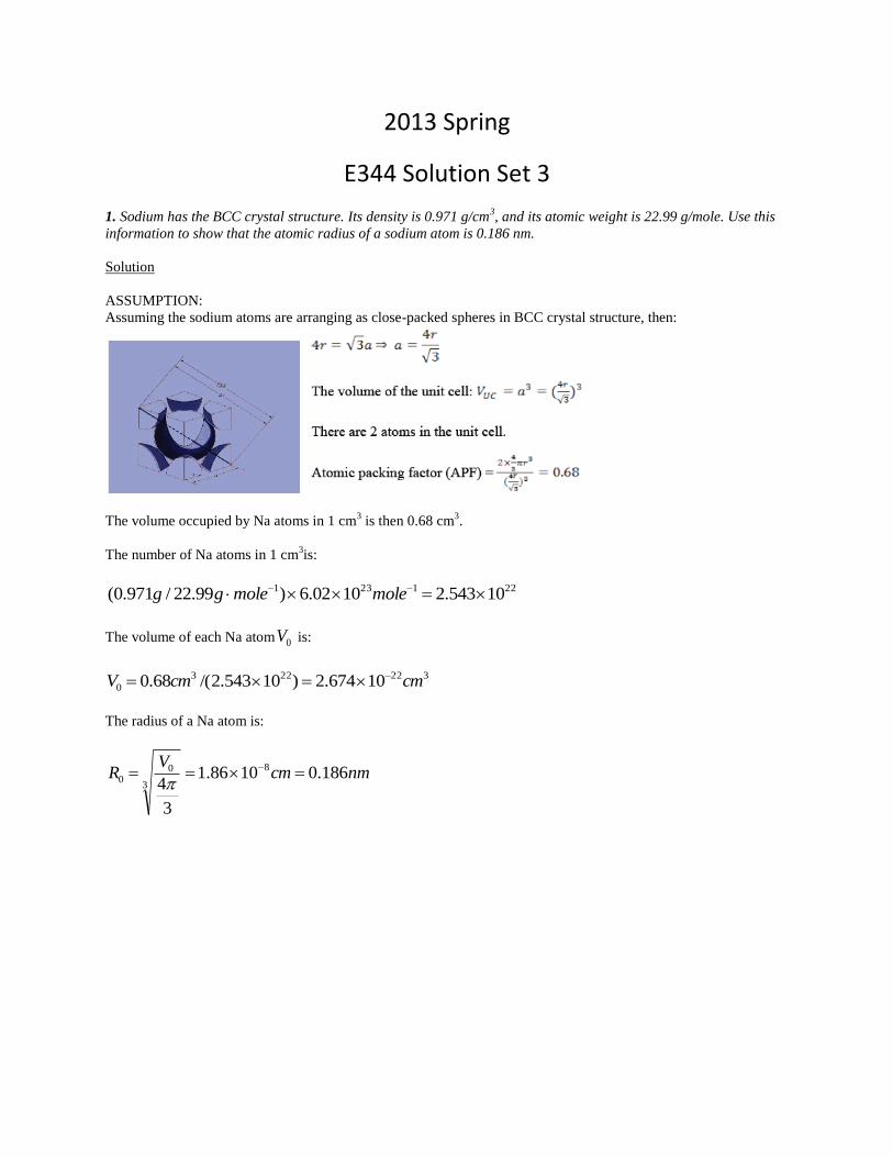
2. Niobium has an atomic radius of 0.1430 nm and a density of 8.57 g/cm3. Determine whether it has an FCC or a
BCC crystal structure. Show all of your work.
Solution
ASSUMPTION:
Assuming the sodium atoms are arranging as close-packed spheres in FCC crystal structure, then
If Niobium has a FCC structure, its density is calculated within one unit cell as:
33213
123
13
2333.91033.9))1430.0(216/(
1002.6
91.924/
1002.6
4cmgnmgnm
mole
molega
M NbFCC
If Niobium has a BCC structure, its density is calculated within one unit cell as:
33213
123
13
2357.81057.8))1430.0(
33
64/(
1002.6
91.922/
1002.6
2cmgnmgnm
mole
molega
M NbFCC
Therefore, Niobium has a BCC structure.
333
222
216)22(
)4(
rraV
raa
uc
There are 4 atoms in a FCC unit cell.
See Problem 1 for BCC structure.
3. 3.23 List the point coordinates of the titanium, barium, and oxygen ions for a unit cell of the perovskite crystal
structure (Figure 12.6).
Solution
In Figure 12.6, the barium ions are situated at all corner positions. The point coordinates for these ions are
as follows: 000, 100, 110, 010, 001, 101, 111, and 011.
The oxygen ions are located at all face-centered positions; therefore, their coordinates are
1
2
1
20,
1
2
1
21,
11
2
1
2,
01
2
1
2,
1
20
1
2, and
1
21
1
2.
And, finally, the titanium ion resides at the center of the cubic unit cell, with coordinates
1
2
1
2
1
2.
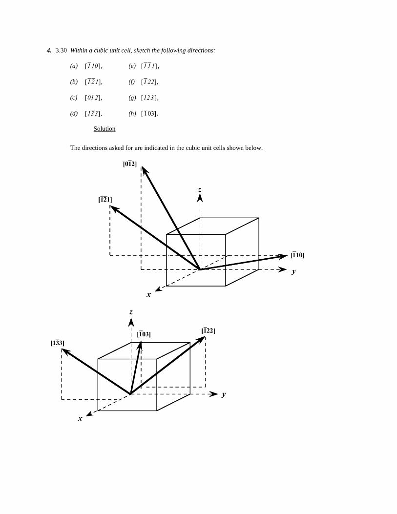
4. 3.30 Within a cubic unit cell, sketch the following directions:
(a)
[1 10] , (e)
[1 1 1] ,
(b)
[1 2 1], (f)
[1 22],
(c)
[01 2], (g)
[12 3 ],
(d)
[13 3], (h)
[1 03].
Solution
The directions asked for are indicated in the cubic unit cells shown below.
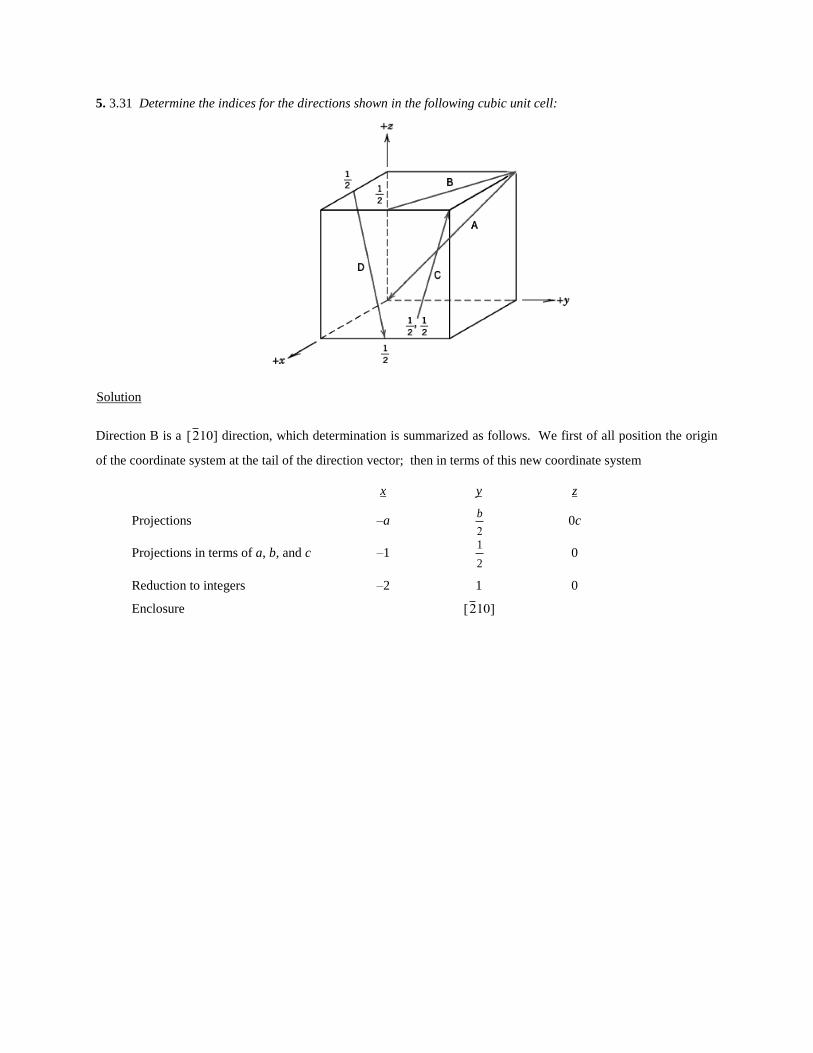
5. 3.31 Determine the indices for the directions shown in the following cubic unit cell:
Solution
Direction B is a
[2 10] direction, which determination is summarized as follows. We first of all position the origin
of the coordinate system at the tail of the direction vector; then in terms of this new coordinate system
x y z
Projections –a
b
2 0c
Projections in terms of a, b, and c –1
1
2 0
Reduction to integers –2 1 0
Enclosure
[2 10]
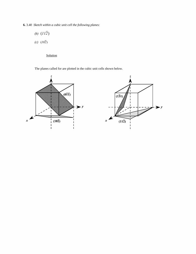
6. 3.40 Sketch within a cubic unit cell the following planes:
(b) )( 211
(c)
(102 )
Solution
The planes called for are plotted in the cubic unit cells shown below.
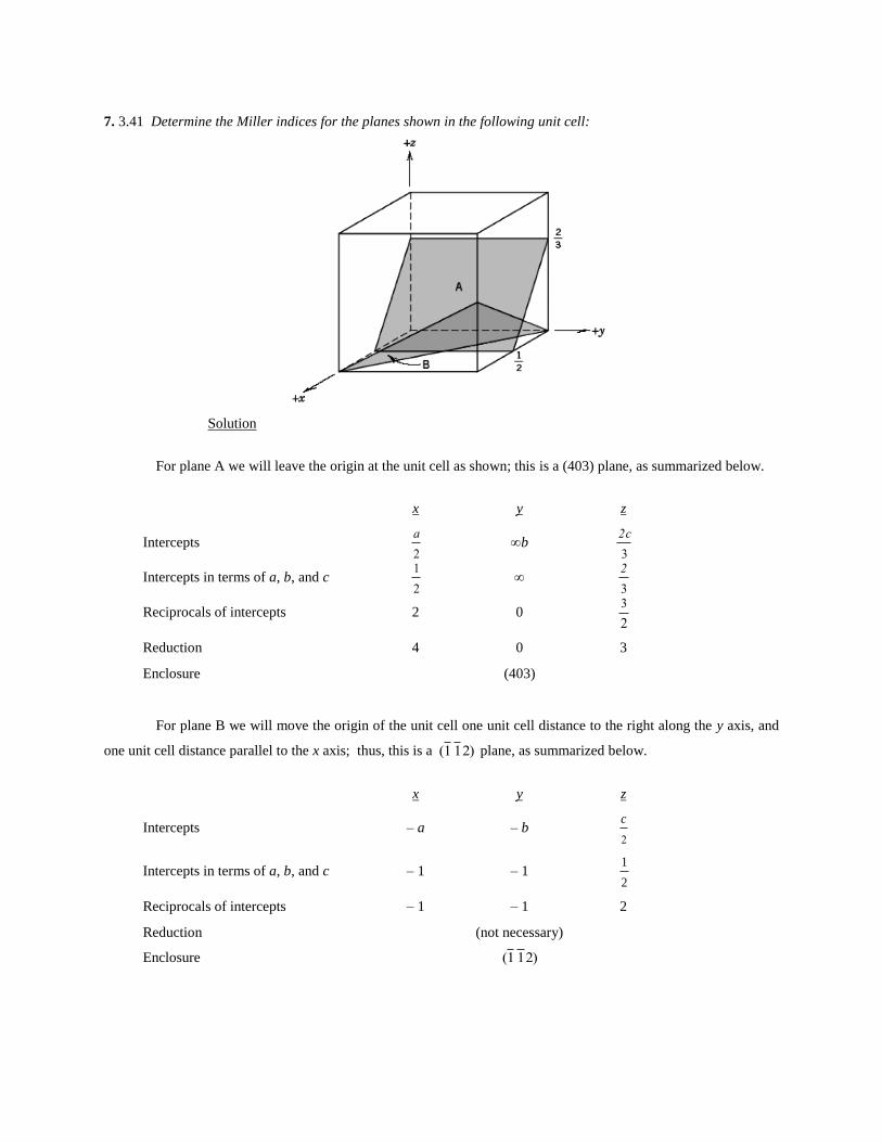
7. 3.41 Determine the Miller indices for the planes shown in the following unit cell:
Solution
For plane A we will leave the origin at the unit cell as shown; this is a (403) plane, as summarized below.
x y z
Intercepts
a
2 b
2c
3
Intercepts in terms of a, b, and c
1
2
2
3
Reciprocals of intercepts 2 0
3
2
Reduction 4 0 3
Enclosure (403)
For plane B we will move the origin of the unit cell one unit cell distance to the right along the y axis, and
one unit cell distance parallel to the x axis; thus, this is a
(1 1 2) plane, as summarized below.
x y z
Intercepts – a – b
c
2
Intercepts in terms of a, b, and c – 1 – 1
1
2
Reciprocals of intercepts – 1 – 1 2
Reduction (not necessary)
Enclosure
(1 1 2)
8. 3.54 (a) Derive planar density expressions for FCC (100) and (111) planes in terms of the atomic radius R.
(b) Compute and compare planar density values for these same two planes for nickel.
Solution
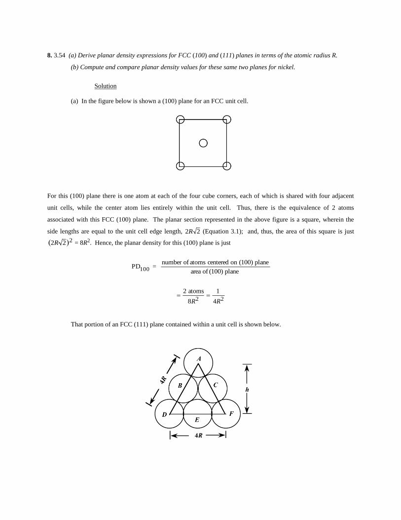
(a) In the figure below is shown a (100) plane for an FCC unit cell.
For this (100) plane there is one atom at each of the four cube corners, each of which is shared with four adjacent
unit cells, while the center atom lies entirely within the unit cell. Thus, there is the equivalence of 2 atoms
associated with this FCC (100) plane. The planar section represented in the above figure is a square, wherein the
side lengths are equal to the unit cell edge length,
2R 2 (Equation 3.1); and, thus, the area of this square is just
(2R 2)2 = 8R2. Hence, the planar density for this (100) plane is just
PD100 = number of atoms centered on (100) plane
area of (100) plane
2 atoms
8R2
1
4R2
That portion of an FCC (111) plane contained within a unit cell is shown below.
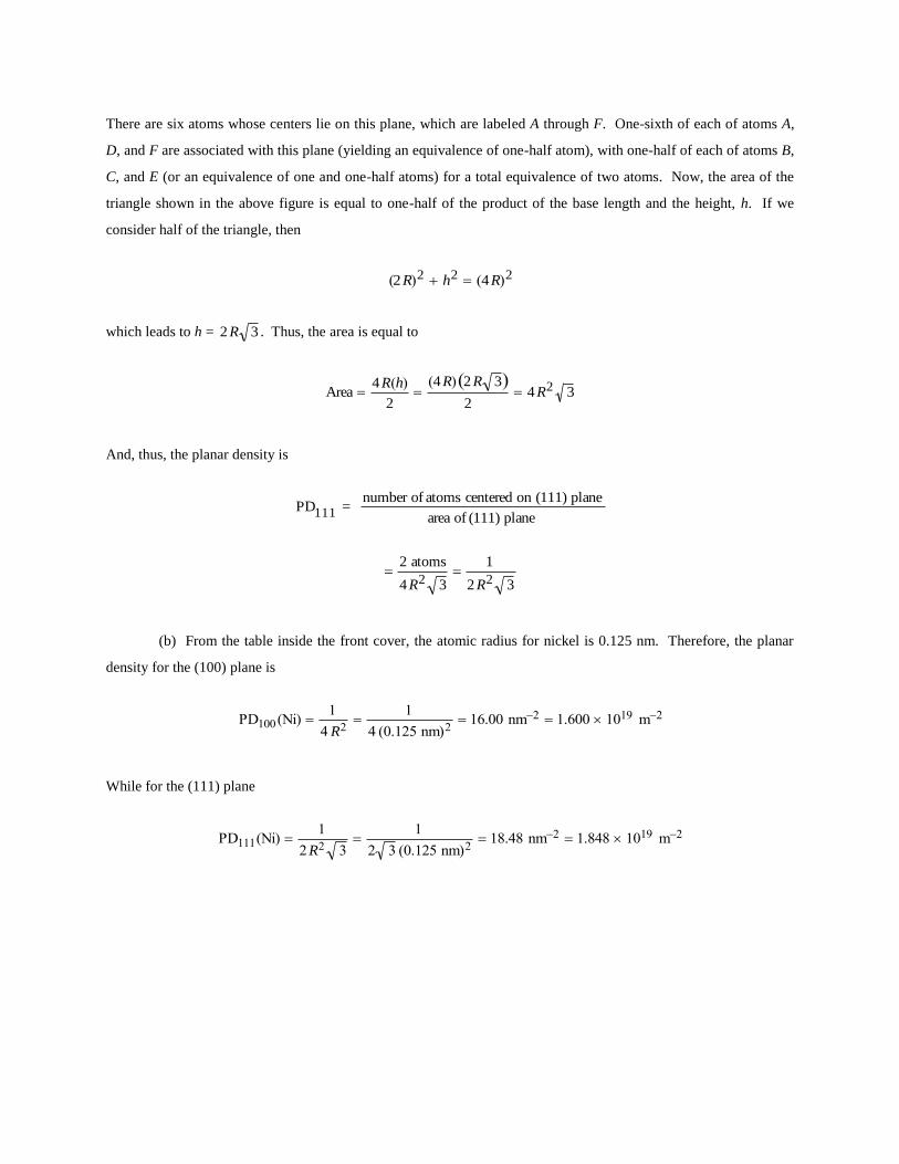
There are six atoms whose centers lie on this plane, which are labeled A through F. One-sixth of each of atoms A,
D, and F are associated with this plane (yielding an equivalence of one-half atom), with one-half of each of atoms B,
C, and E (or an equivalence of one and one-half atoms) for a total equivalence of two atoms. Now, the area of the
triangle shown in the above figure is equal to one-half of the product of the base length and the height, h. If we
consider half of the triangle, then
(2R)2 h2 (4R)2
which leads to h =
2 R 3 . Thus, the area is equal to
Area 4 R(h)
2
(4 R)(2 R 3)
2 4 R2 3
And, thus, the planar density is
PD111 = number of atoms centered on (111) plane
area of (111) plane
2 atoms
4 R2 3
1
2 R2 3
(b) From the table inside the front cover, the atomic radius for nickel is 0.125 nm. Therefore, the planar
density for the (100) plane is
PD100 (Ni) 1
4 R2
1
4 (0.125 nm)2 16.00 nm2 1.600 1019 m2
While for the (111) plane
PD111(Ni) 1
2 R2 3
1
2 3 (0.125 nm)2 18.48 nm2 1.848 1019 m2
9. 4.27 For an FCC single crystal, would you expect the surface energy for a (100) plane to be greater or less than
that for a (111) plane? Why? (Note: You may want to consult the solution to Problem 3.54 at the end of Chapter 3.)
Solution
The surface energy for a crystallographic plane will depend on its packing density [i.e., the planar density
(Section 3.11)]—that is, the higher the packing density, the greater the number of nearest-neighbor atoms, and the
more atomic bonds in that plane that are satisfied, and, consequently, the lower the surface energy. From the
solution to Problem 3.54, planar densities for FCC (100) and (111) planes are
1
4R2 and
1
2R2 3, respectively—that
is
0.25
R2 and
0.29
R2 (where R is the atomic radius). Thus, since the planar density for (111) is greater, it will have the
lower surface energy.
10. One way to describe a crystal structure is to use a simple unit cell with a multi-atom basis.
The "basis" represents the set of atoms that is translated to each point in a unit cell to create the
crystal structure. For example, silver (Ag) is FCC with a one-atom basis. That one atom would
have coordinates of (0,0,0). Similarly, silicon (Si) has the diamond-cubic crystal structure, which
can be described as FCC with a two-atom basis. The basis would consists of a Si atom at (0,0,0)
and another Si atom at (¼, ¼, ¼ ). If these two atoms are translated to all of the corner and face
positions of the FCC unit cell, the diamond cubic lattice is created.
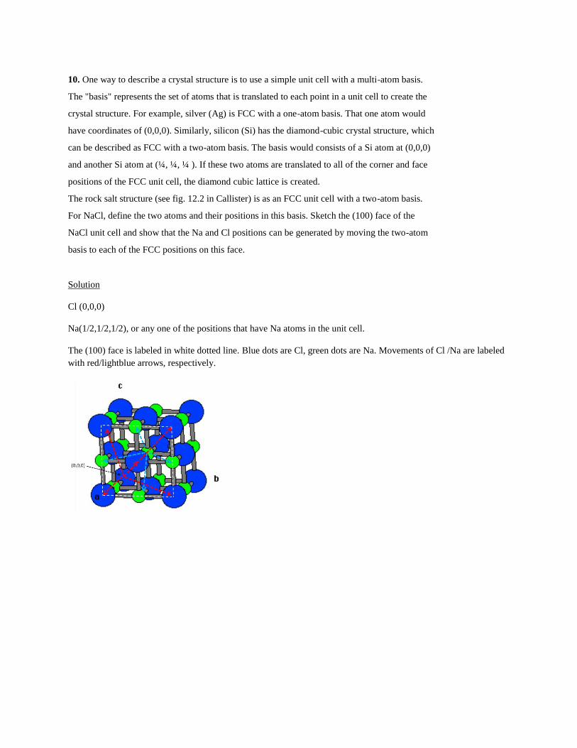
The rock salt structure (see fig. 12.2 in Callister) is as an FCC unit cell with a two-atom basis.
For NaCl, define the two atoms and their positions in this basis. Sketch the (100) face of the
NaCl unit cell and show that the Na and Cl positions can be generated by moving the two-atom
basis to each of the FCC positions on this face.
Solution
Cl (0,0,0)
Na(1/2,1/2,1/2), or any one of the positions that have Na atoms in the unit cell.
The (100) face is labeled in white dotted line. Blue dots are Cl, green dots are Na. Movements of Cl /Na are labeled
with red/lightblue arrows, respectively.
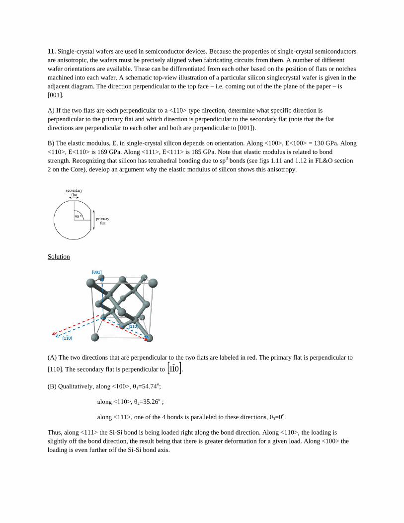
11. Single-crystal wafers are used in semiconductor devices. Because the properties of single-crystal semiconductors
are anisotropic, the wafers must be precisely aligned when fabricating circuits from them. A number of different
wafer orientations are available. These can be differentiated from each other based on the position of flats or notches
machined into each wafer. A schematic top-view illustration of a particular silicon singlecrystal wafer is given in the
adjacent diagram. The direction perpendicular to the top face – i.e. coming out of the the plane of the paper – is
[001].
A) If the two flats are each perpendicular to a <110> type direction, determine what specific direction is
perpendicular to the primary flat and which direction is perpendicular to the secondary flat (note that the flat
directions are perpendicular to each other and both are perpendicular to [001]).
B) The elastic modulus, E, in single-crystal silicon depends on orientation. Along <100>, E<100> = 130 GPa. Along
<110>, E<110> is 169 GPa. Along <111>, E<111> is 185 GPa. Note that elastic modulus is related to bond
strength. Recognizing that silicon has tetrahedral bonding due to sp3 bonds (see figs 1.11 and 1.12 in FL&O section
2 on the Core), develop an argument why the elastic modulus of silicon shows this anisotropy.
Solution
(A) The two directions that are perpendicular to the two flats are labeled in red. The primary flat is perpendicular to
[110]. The secondary flat is perpendicular to 011 .
(B) Qualitatively, along <100>, θ1=54.74ο;
along <110>, θ2=35.26ο ;
along <111>, one of the 4 bonds is paralleled to these directions, θ3=0ο.
Thus, along <111> the Si-Si bond is being loaded right along the bond direction. Along <110>, the loading is
slightly off the bond direction, the result being that there is greater deformation for a given load. Along <100> the
loading is even further off the Si-Si bond axis.

12. In Callister read/skim: pages 6+7 on ceramics; sections 12.1, 12.2, and 12.3
13. A
14. B