Pipelining & Verilog - MITweb.mit.edu/6.111/www/f2017/handouts/L09.pdf · Pipelining & Verilog •...
48
Pipelining & Verilog • 6.UAP? • Division • Latency & Throughput • Pipelining to increase throughput • Retiming • Verilog Math Functions 1 Lecture 9 6.111 Fall 2017
Transcript of Pipelining & Verilog - MITweb.mit.edu/6.111/www/f2017/handouts/L09.pdf · Pipelining & Verilog •...

Pipelining & Verilog• 6.UAP? • Division• Latency & Throughput• Pipelining to increase throughput• Retiming• Verilog Math Functions
1Lecture 96.111 Fall 2017

Cyclic redundancy check - CRC
CRC16 (x16 + x15 + x2 + 1)
x16 r[15] r[14] + r[15] + x16
• Each “r” is a register, all clocked with a common clock. Common clock not shown
• As shown, for register r15, the output is r[15] and the input is the sum of r[14], r[15] and data input x16, etc
• The small round circles with the plus sign are adders implemented with XOR gates.
• Initialize r to 16’hFFFF at start
The CRC-16 detects all single errors, all double bit errors and all errors with burst less than 16 bits in length.

CRC Solution CRC16: x16+x15+x2+1
Sequential Divider
Lecture 9 4
Assume the Dividend (A) and the divisor (B) have N bits. If we only want to invest in a single N-bit adder, we can build a sequential circuit that processes a single subtraction at a time and then cycle the circuit N times. This circuit works on unsigned operands; for signed operands one can remember the signs, make operands positive, then correct sign of result.
BP A
-
S
N+1N+1
N+1
Init: P0, load A and BRepeat N times {
shift P/A left one bittemp = P-Bif (temp > 0){Ptemp, ALSB1}
else ALSB0}Done: Q in A, R in P
N bits
LSB
0
>0? S
S0 1
6.111 Fall 2017
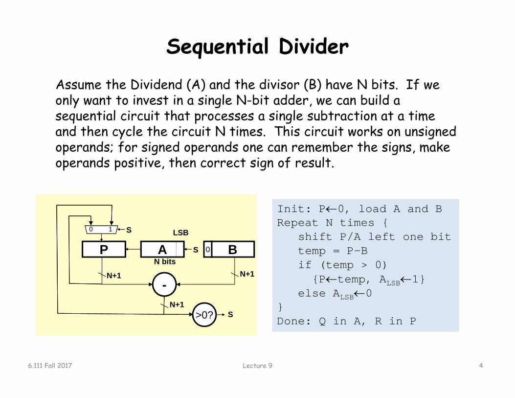
Sequential Divider
Lecture 9 5
Init: P0, load A and BRepeat N times {
shift P/A left one bittemp = P-Bif (temp > 0){Ptemp, ALSB1}
else ALSB0}Done: Q in A, R in P
6.111 Fall 2017
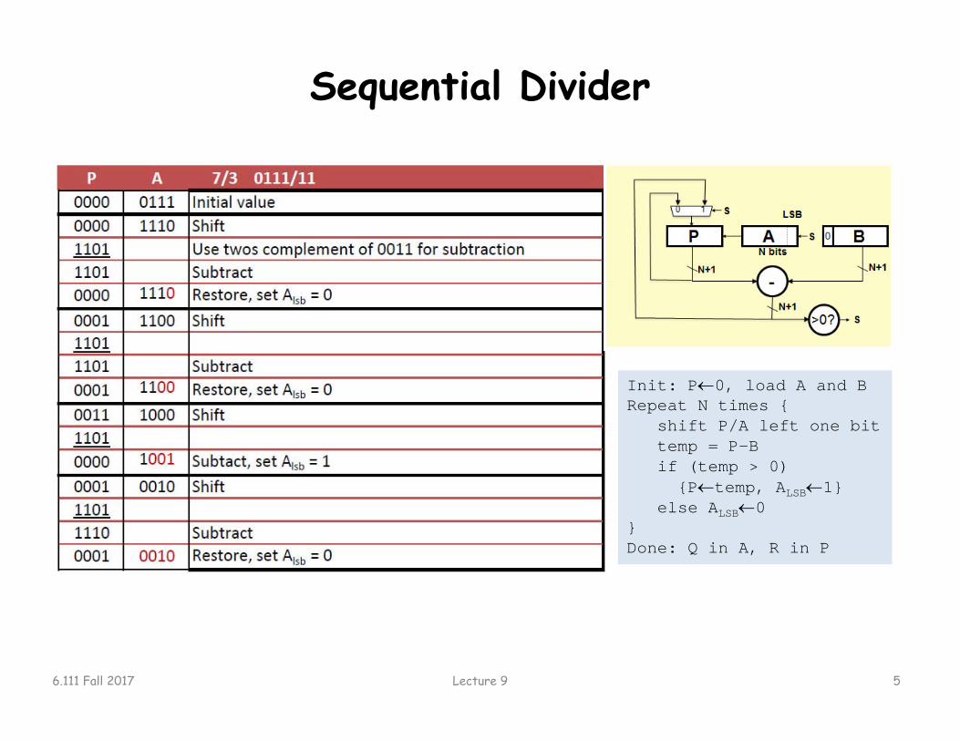
Verilog divider.v// The divider module divides one number by another. It// produces a signal named "ready" when the quotient output// is ready, and takes a signal named "start" to indicate// the the input dividend and divider is ready.// sign -- 0 for unsigned, 1 for twos complement
// It uses a simple restoring divide algorithm.// http://en.wikipedia.org/wiki/Division_(digital)#Restoring_division
module divider #(parameter WIDTH = 8) (input clk, sign, start,input [WIDTH-1:0] dividend, input [WIDTH-1:0] divider,output reg [WIDTH-1:0] quotient,output [WIDTH-1:0] remainder;output ready);
reg [WIDTH-1:0] quotient_temp;reg [WIDTH*2-1:0] dividend_copy, divider_copy, diff;reg negative_output;
wire [WIDTH-1:0] remainder = (!negative_output) ?dividend_copy[WIDTH-1:0] : ~dividend_copy[WIDTH-1:0] + 1'b1;
reg [5:0] bit;reg del_ready = 1;wire ready = (!bit) & ~del_ready;
wire [WIDTH-2:0] zeros = 0;initial bit = 0;initial negative_output = 0;
always @( posedge clk ) begindel_ready <= !bit;if( start ) begin
bit = WIDTH;quotient = 0;quotient_temp = 0;dividend_copy = (!sign || !dividend[WIDTH-1]) ?
{1'b0,zeros,dividend} : {1'b0,zeros,~dividend + 1'b1};
divider_copy = (!sign || !divider[WIDTH-1]) ?{1'b0,divider,zeros} :{1'b0,~divider + 1'b1,zeros};
negative_output = sign &&((divider[WIDTH-1] && !dividend[WIDTH-1])||(!divider[WIDTH-1] && dividend[WIDTH-1]));
endelse if ( bit > 0 ) begin
diff = dividend_copy - divider_copy;quotient_temp = quotient_temp << 1;if( !diff[WIDTH*2-1] ) begin
dividend_copy = diff;quotient_temp[0] = 1'd1;
endquotient = (!negative_output) ?
quotient_temp :~quotient_temp + 1'b1;
divider_copy = divider_copy >> 1;bit = bit - 1'b1;
endend
endmodule
6.111 Fall 2017 Lecture 9 6L. Williams MIT ‘13

Math Functions in Coregen
7Lecture 9
Wide selection of math functions available
6.111 Fall 2017
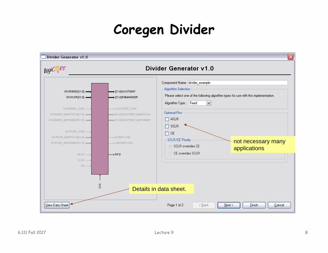
Coregen Divider
6.111 Fall 2017 8Lecture 9
not necessary many applications
Details in data sheet.
Lecture 9 86.111 Fall 2017

Coregen Divider
6.111 Fall 2017 9Lecture 9
Chose minimium number for application
Ready For Data: needed if clocks/divide >1
Lecture 9 96.111 Fall 2017

Performance Metrics for Circuits
time between arrival of new input and generation of corresponding output.
For combinational circuits this is just tPD.
Circuit Latency (L):
Rate at which new outputs appear.
For combinational circuits this is just 1/tPD or 1/L.
Circuit Throughput (T):
6.111 Fall 2017 10Lecture 9Lecture 9 106.111 Fall 2017

Coregen Divider Latency
6.111 Fall 2017 11Lecture 9
Latency dependent on dividend width + fractioanl reminder width
Lecture 9 116.111 Fall 2017

Performance of Combinational Circuits
F
G
HX P(X)
For combinational logic:L = tPD, T = 1/tPD.
We can’t get the answer faster, but are we making effective use of our hardware at all times?
G(X)F(X)
P(X)
X
F & G are “idle”, just holding their outputs stable while H performs its computation
12Lecture 96.111 Fall 2017

Retiming is the action of moving registers around in the system Registers have to be moved from ALL inputs to ALL outputs or vice versa
Retiming: A very useful transform
Cutset retiming: A cutset intersects the edges, such that this would result in two disjoint partitions of the edges being cut. To retime, delays are moved from the ingoing to the outgoing edges or vice versa.
Benefits of retiming:• Modify critical path delay• Reduce total number of registers
13Lecture 96.111 Fall 2017

Retiming Combinational Circuitsaka “Pipelining”
P(X)
15
20
25X
L = 45T = 1/45
P(Xi-2)
15
20
25Xi
tCLK = 25L = 2*tCLK = 50T = 1/tCLK = 1/25
Assuming ideal registers:i.e., tPD = 0, tSETUP = 0
14Lecture 96.111 Fall 2017

Pipeline diagrams
Input
F Reg
G Reg
H Reg
i i+1 i+2 i+3
Xi Xi+1
F(Xi)
G(Xi)
Xi+2
F(Xi+1)
G(Xi+1)
H(Xi)
Xi+3
F(Xi+2)
G(Xi+2)
H(Xi+1)
Clock cyclePi
pelin
e st
ages
The results associated with a particular set of input data moves diagonally through the diagram, progressing through one pipeline stage each clock cycle.
H(Xi+2)
…
…
F
G
HX P(X)
15
20
25
15Lecture 96.111 Fall 2017
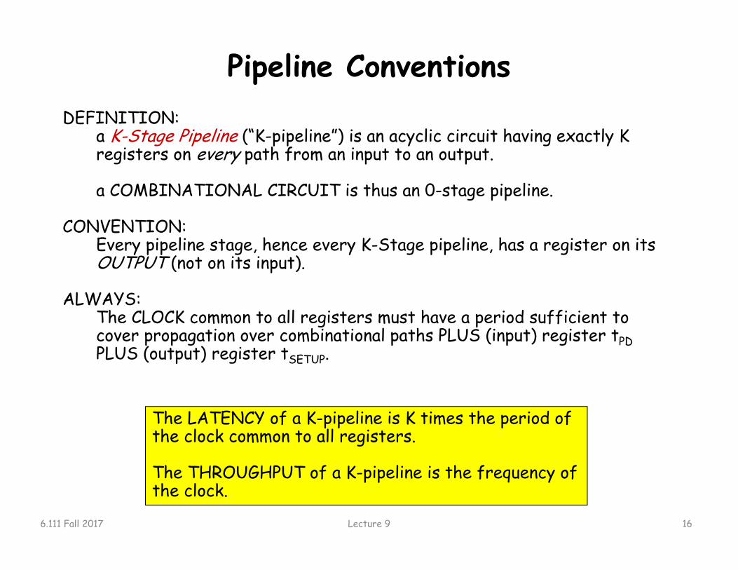
Pipeline ConventionsDEFINITION:
a K-Stage Pipeline (“K-pipeline”) is an acyclic circuit having exactly K registers on every path from an input to an output.
a COMBINATIONAL CIRCUIT is thus an 0-stage pipeline.
CONVENTION:Every pipeline stage, hence every K-Stage pipeline, has a register on its OUTPUT (not on its input).
ALWAYS:The CLOCK common to all registers must have a period sufficient to cover propagation over combinational paths PLUS (input) register tPDPLUS (output) register tSETUP.
The LATENCY of a K-pipeline is K times the period of the clock common to all registers.
The THROUGHPUT of a K-pipeline is the frequency of the clock.
16Lecture 96.111 Fall 2017
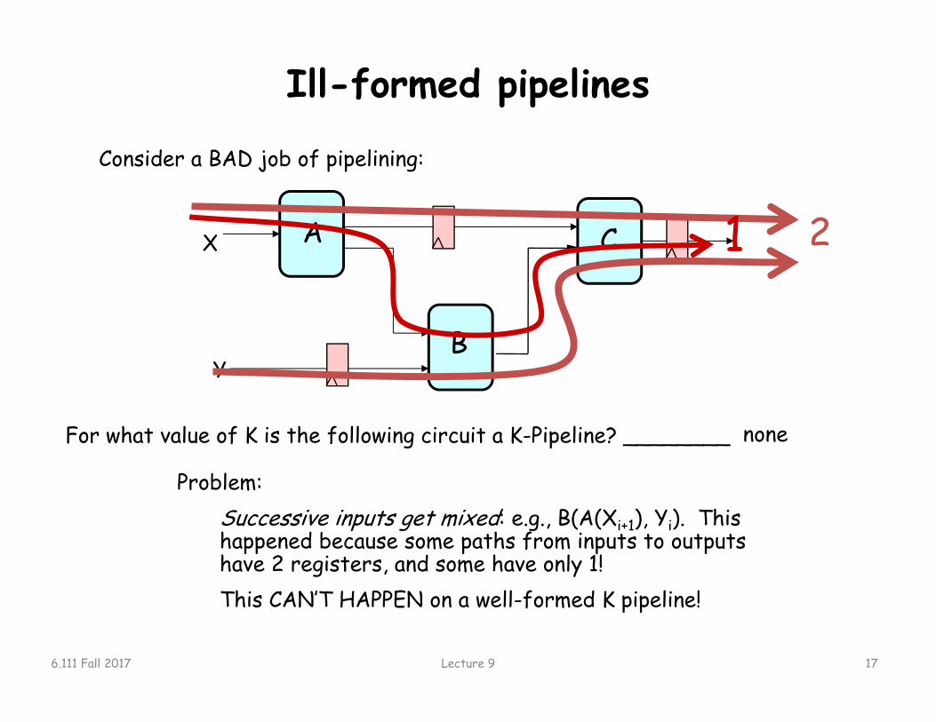
Ill-formed pipelines
B
CX
Y
A
Problem:Successive inputs get mixed: e.g., B(A(Xi+1), Yi). This happened because some paths from inputs to outputs have 2 registers, and some have only 1!This CAN’T HAPPEN on a well-formed K pipeline!
noneFor what value of K is the following circuit a K-Pipeline? ________
Consider a BAD job of pipelining:
21
17Lecture 96.111 Fall 2017

A pipelining methodologyStep 1:Add a register on each output.
Step 2:Add another register on each output. Draw a cut-set contour that includes all the new registers and some part of the circuit. Retime by moving regs from all outputs to all inputs of cut-set.
Repeat until satisfied with T.
STRATEGY:Focus your attention on placing pipelining registers around the slowest circuit elements (BOTTLENECKS).
A4 nS
B3 nS
C8 nS
D4 nS
E2 nS
F5 nS
T = 1/8nsL = 24ns
18Lecture 96.111 Fall 2017

Pipeline Example
A
B
CX
Y
2
1
1
0-pipe:LATENCY THROUGHPUT
4 1/4
OBSERVATIONS:• 1-pipeline improves
neither L or T.• T improved by breaking
long combinational paths, allowing faster clock.
• Too many stages cost L, don’t improve T.
• Back-to-back registers are often required to keep pipeline well-formed.1-pipe: 4 1/4
1
2-pipe: 4 1/2
2
2
3-pipe: 1/26
3
3
19Lecture 96.111 Fall 2017

Pipeline Example - VerilogLab 3 Pong• G = game logic 8ns tpd• C = draw round puck, use
multiply with 9ns tpd• System clock 65mhz =
15ns period – opps
20Lecture 96.111 Fall 2017
G CX
hcount,vcount,
etc
8 9
pixel
Yintermediate
wires
G CX8 9
pixelY Y2
No pipelineassign y = G(x); // logic for y assign pixel = C(y) // logic for pixel
clock clock
Pipelinealways @(posedge clock) begin
...y2 <= G(x); // pipeline ypixel <= C(y2) // pipeline pixel
end
reg [N:0] x,y;reg [23:0] pixelalways @ * begin
y=G(x);pixel = C(y);
end
Latency = 2 clock cyles!Implications?

Increasing Throughput: Pipelining
= register
Idea: split processing across several clock cycles by dividing circuit into pipeline stages separated by registers that hold values passing from one stage to the next.
Throughput = 1/4tPD,FA instead of 1/8tPD,FA)21Lecture 96.111 Fall 2017
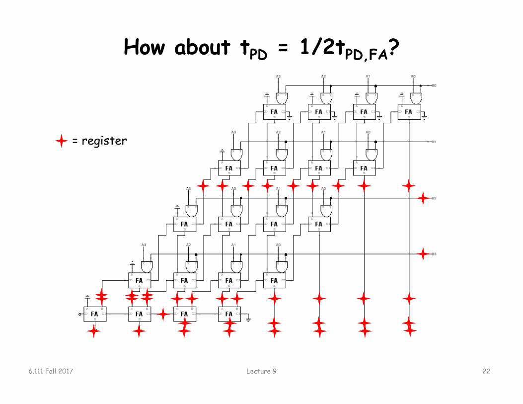
How about tPD = 1/2tPD,FA?
Lecture 9 22
= register
6.111 Fall 2017

Timing Reports
Lecture 9 23
Multiple: 7.251ns
65mhz = 27mhz*2.4
Synthesis report
Total Propagation delay: 34.8ns
6.111 Fall 2017

History of Computational Fabrics Discrete devices: relays, transistors (1940s-50s) Discrete logic gates (1950s-60s) Integrated circuits (1960s-70s)
e.g. TTL packages: Data Book for 100’s of different parts Gate Arrays (IBM 1970s)
Transistors are pre-placed on the chip & Place and Route software puts the chip together automatically – only program the interconnect (mask programming)
Software Based Schemes (1970’s- present) Run instructions on a general purpose core
Programmable Logic (1980’s to present) A chip that be reprogrammed after it has been fabricated Examples: PALs, EPROM, EEPROM, PLDs, FPGAs Excellent support for mapping from Verilog
ASIC Design (1980’s to present) Turn Verilog directly into layout using a library of standard cells Effective for high-volume and efficient use of silicon area
Lecture 9 246.111 Fall 2017

Reconfigurable Logic
• Logic blocks– To implement combinational
and sequential logic• Interconnect
– Wires to connect inputs andoutputs to logic blocks
• I/O blocks– Special logic blocks at
periphery of device forexternal connections
• Key questions:– How to make logic blocks programmable?
(after chip has been fabbed!)– What should the logic granularity be?– How to make the wires programmable?
(after chip has been fabbed!)– Specialized wiring structures for local
vs. long distance routes?– How many wires per logic block?
LogicLogic
Configuration
Inputs Outputsn m
Q
QSET
CLR
D
Lecture 9 256.111 Fall 2017

Programmable Array Logic (PAL)
• Based on the fact that any combinational logic can be realized as a sum-of-products
• PALs feature an array of AND-OR gates with programmable interconnect
inputsignals
outputsignals
programming of product terms
programming of sum terms
ANDarray OR array
Lecture 9 266.111 Fall 2017

RAM Based Field Programmable Logic - Xilinx
CLB
CLB
CLB
CLB
SwitchMatrix
ProgrammableInterconnect I/O Blocks (IOBs)
ConfigurableLogic Blocks (CLBs)
D Q
SlewRate
Control
PassivePull-Up,
Pull-Down
Delay
Vcc
OutputBuffer
InputBuffer
Q D
Pad
D QSD
RDEC
S/RControl
D QSD
RDEC
S/RControl
1
1
F'G'
H'
DIN
F'G'
H'
DIN
F'
G'H'
H'
HFunc.Gen.
GFunc.Gen.
FFunc.Gen.
G4G3G2G1
F4F3F2F1
C4C1 C2 C3
K
Y
X
H1 DIN S/R EC
Lecture 9 276.111 Fall 2017

LUT Mapping
• N-LUT direct implementation of a truth table: any function of n-inputs.
• N-LUT requires 2N storage elements (latches)• N-inputs select one latch location (like a memory)
4LUT example
Latches set by configuration bitstream
Inputs
Output
Lecture 9 286.111 Fall 2017

Configuring the CLB as a RAM
Memory is built using Latches not FFs
Read is same a LUT Function!
16x2
Lecture 9 296.111 Fall 2017

Xilinx 4000 Interconnect
Lecture 9 306.111 Fall 2017

Xilinx 4000 Interconnect Details
Wires are not ideal!
Lecture 9 316.111 Fall 2017
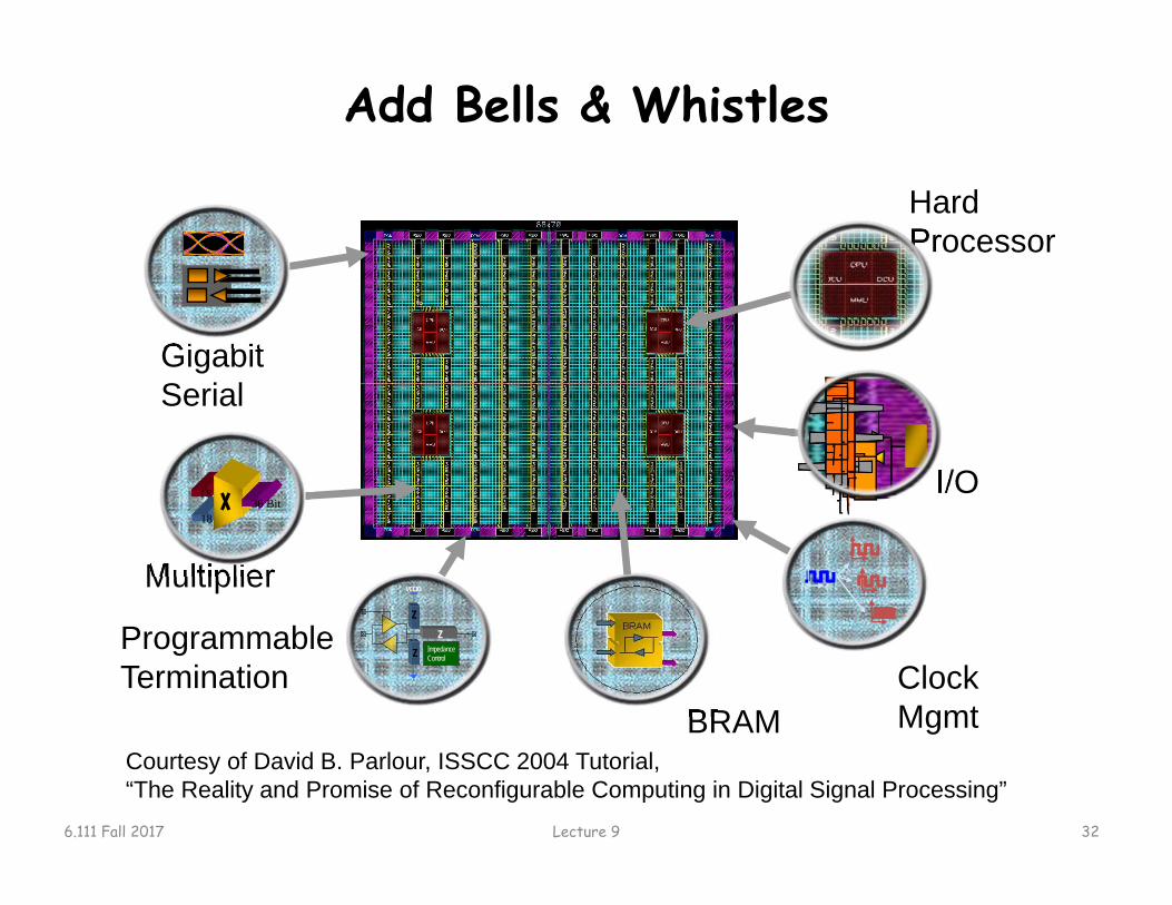
Add Bells & Whistles
HardProcessor
I/O
BRAM
Gigabit Serial
Multiplier
ProgrammableTermination
Z
VCCIO
Z
Z
ImpedanceControl
ClockMgmt
18 Bit
18 Bit36 Bit
Courtesy of David B. Parlour, ISSCC 2004 Tutorial, “The Reality and Promise of Reconfigurable Computing in Digital Signal Processing”
Lecture 9 326.111 Fall 2017

The Virtex II CLB (Half Slice Shown)
Lecture 9 336.111 Fall 2017
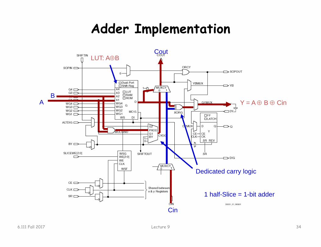
Adder Implementation
Y = A B CinAB
Cin
CoutLUT: AB
1 half-Slice = 1-bit adder
Dedicated carry logic
Lecture 9 346.111 Fall 2017

FPGA’s
CLB Dist RAM Block RAM Multipliers
Virtex 2 8,448 1,056 kbit 2,592 kbit 144 (18x18)Virtex 6 667,000 6,200 kbit 22,752 kbit 1,344 (25x18)Spartan 3E 240 15 kbit 72 kbit 4 (18x18)Artix-7 A100 7,925 1,188 kbit 4,860 kbit 240 (25x18)
DSP with 25x18 multiplier
Gigabit ethernet support
Lecture 9 356.111 Fall 2017
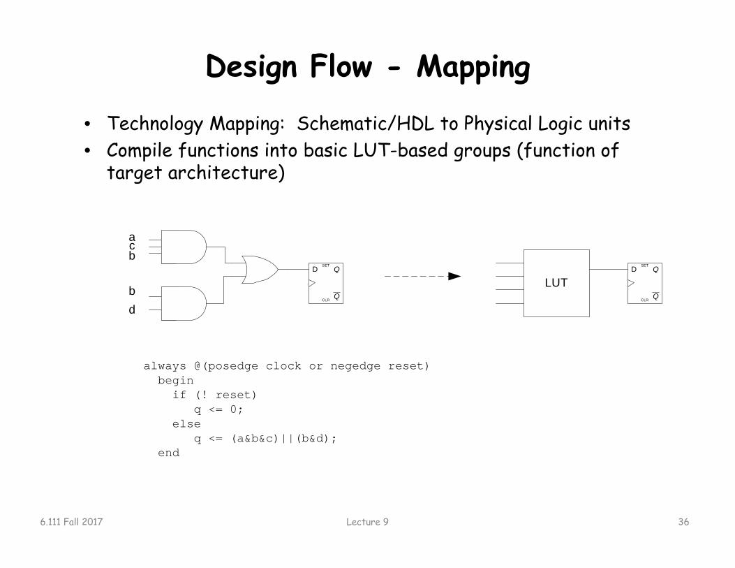
Design Flow - Mapping
• Technology Mapping: Schematic/HDL to Physical Logic units• Compile functions into basic LUT-based groups (function of
target architecture)
always @(posedge clock or negedge reset)beginif (! reset)
q <= 0;else
q <= (a&b&c)||(b&d);end
Q
QSET
CLR
D
LUTQ
QSET
CLR
D
abc
db
Lecture 9 366.111 Fall 2017

Design Flow – Placement & Route• Placement – assign logic location on a particular device
LUT
LUT
LUT
Routing – iterative process to connect CLB inputs/outputs and IOBs. Optimizes critical path delay – can take hours or days for large, dense designs
Iterate placement if timing not met
Satisfy timing? Generate Bitstream to config device
Challenge! Cannot use full chip for reasonable speeds (wires are not ideal).
Typically no more than 50% utilization.Lecture 9 376.111 Fall 2017

Example: Verilog to FPGA
module adder64 ( input [63:0] a, b; output [63:0] sum);
assign sum = a + b;endmodule
Virtex II – XC2V2000
• Synthesis• Tech Map• Place&Route
64-bit Adder Example
Lecture 9 386.111 Fall 2017
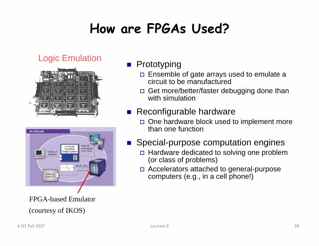
How are FPGAs Used?
(courtesy of IKOS)FPGA-based Emulator
Logic Emulation Prototyping
Ensemble of gate arrays used to emulate a circuit to be manufactured
Get more/better/faster debugging done than with simulation
Reconfigurable hardware One hardware block used to implement more
than one function
Special-purpose computation engines Hardware dedicated to solving one problem
(or class of problems) Accelerators attached to general-purpose
computers (e.g., in a cell phone!)
Lecture 9 396.111 Fall 2017
Summary
• FPGA provide a flexible platform for implementing digital computing
• A rich set of macros and I/Os supported (multipliers, block RAMS, ROMS, high-speed I/O)
• A wide range of applications from prototyping (to validate a design before ASIC mapping) to high-performance spatial computing
• Interconnects are a major bottleneck (physical design and locality are important considerations)
Lecture 9 406.111 Fall 2017
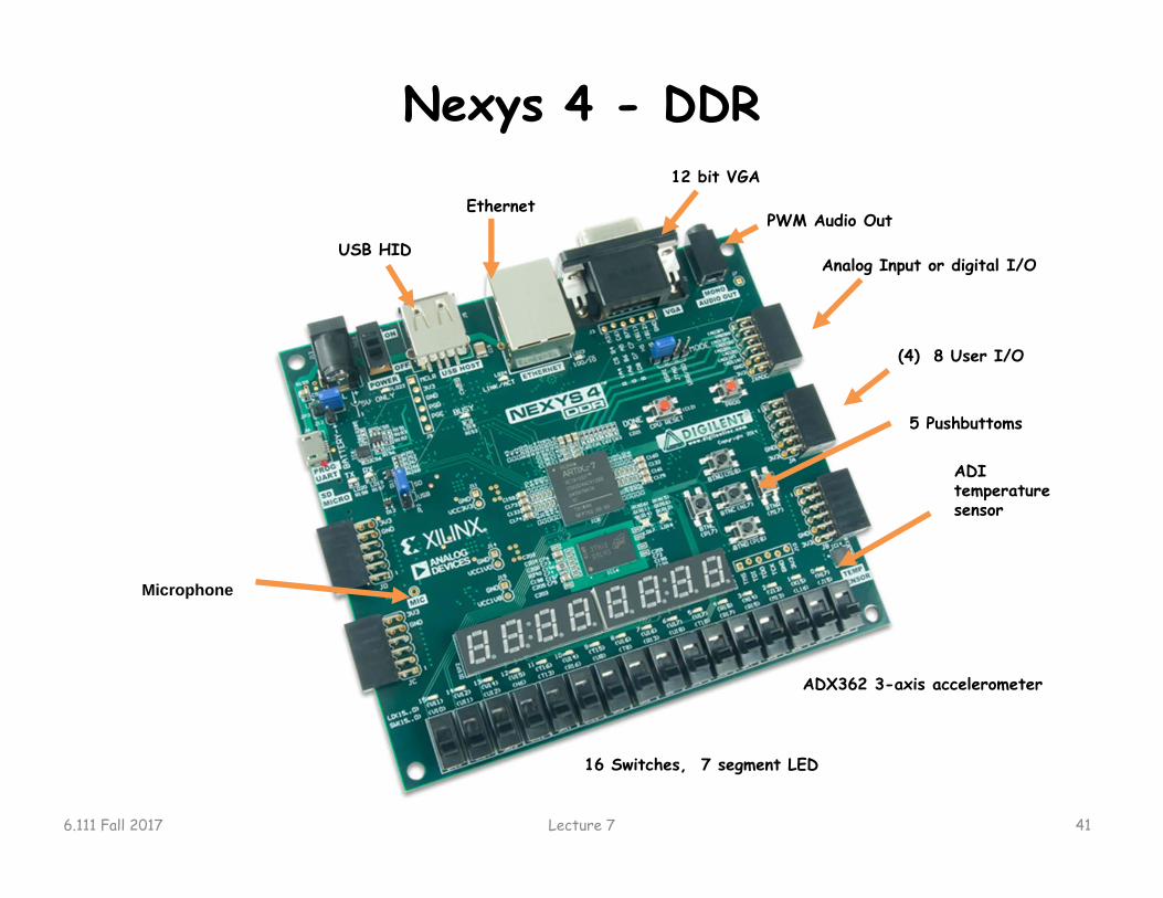
Nexys 4 - DDR
6.111 Fall 2017 Lecture 7 41
Analog Input or digital I/O
16 Switches, 7 segment LED
PWM Audio Out
Microphone
(4) 8 User I/O
12 bit VGA
ADI temperaturesensor
Ethernet
USB HID
5 Pushbuttoms
ADX362 3-axis accelerometer

Nexy4 Input Outputmodule labkit(
input CLK100MHZ,input[15:0] SW, input BTNC, BTNU, BTNL, BTNR, BTND,output[3:0] VGA_R, output[3:0] VGA_B, output[3:0] VGA_G,output[7:0] JA, output VGA_HS, output VGA_VS, output LED16_B, LED16_G, LED16_R,output LED17_B, LED17_G, LED17_R,output[15:0] LED,output[7:0] SEG, // segments A-G (0-6), DP (7)output[7:0] AN // Display 0-7);
assign data = {28'h0123456, SW[3:0]}; // display 0123456 + SW
6.111 Fall 2017 Lecture 9 42

XDC Fileset_property -dict { PACKAGE_PIN N17 IOSTANDARD LVCMOS33 } [get_ports { BTNC }];
#IO_L9P_T1_DQS_14 Sch=btnc
set_property -dict { PACKAGE_PIN M18 IOSTANDARD LVCMOS33 } [get_ports { BTNU }]; #IO_L4N_T0_D05_14 Sch=btnu
set_property -dict { PACKAGE_PIN P17 IOSTANDARD LVCMOS33 } [get_ports { BTNL }]; #IO_L12P_T1_MRCC_14 Sch=btnl
set_property -dict { PACKAGE_PIN M17 IOSTANDARD LVCMOS33 } [get_ports { BTNR }]; #IO_L10N_T1_D15_14 Sch=btnr
set_property -dict { PACKAGE_PIN P18 IOSTANDARD LVCMOS33 } [get_ports { BTND }]; #IO_L9N_T1_DQS_D13_14 Sch=btnd
6.111 Fall 2017 Lecture 9 43

Dashboard
6.111 Fall 2017 Lecture 9 44

Loading Nexys4 Flash
1. Format a flash drive to have 1 fat32 partition
2. In vivado, click generate bitstream and afterwards do file->Export->Export_Bitstream_File to flash top-level directory
3. On the nexys 4, switch jumper JP1 to be on the USB/SD mode
4. Plug the usb stick into the nexys 4 while it's off and then power on. A yellow LED will flash while the bitstream is being loaded. When it's done, the green DONE led will turn on
5. You can remove the usb drive after your code is running
6.111 Fall 2017 Lecture 9 45

Vivado Simulation
6.111 Fall 2017 Lecture 9 46

6.111 Fall 2017 Lecture 9 47

Test Bench
6.111 Fall 2017 Lecture 9 48
module sample_tf; // Inputs module sample(reg bit_in; input bit_in,reg [3:0] bus_in; input [3:0] bus_in,
// Outputs output out_bit,wire out_bit; output [7:0] out_buswire [7:0] out_bus; );
. . . Verilog . . . // Instantiate the Unit Under Test (UUT)sample uut ( endmodule
.bit_in(bit_in),
.bus_in(bus_in),
.out_bit(out_bit),
.out_bus(out_bus));
initial begin// Initialize Inputsbit_in = 0;bus_in = 0;
// Wait 100 ns for global reset to finish#100;
// Add stimulus here
end
endmodule
inputs must be initialized


![lec5-pipeline 1.ppt [Uyumluluk Modu]eem.eskisehir.edu.tr/userfiles/atdogan/files/lec7-pipeline_1.pdfPipelining Lessons Pipelining doesn’t help latency of single task, it helps throughput](https://static.fdocuments.net/doc/165x107/5e176b9bee70db24c74777ae/lec5-pipeline-1ppt-uyumluluk-modueem-lessons-pipelining-doesnat-help-latency.jpg)