
Piezoelectric metal oxide nanostructures for energy harvesting Reza Saberi Moghaddam.
24
Piezoelectric metal oxide nanostructures for energy harvesting Reza Saberi Moghaddam
-
Upload
christina-walsh -
Category
Documents
-
view
228 -
download
4
Transcript of Piezoelectric metal oxide nanostructures for energy harvesting Reza Saberi Moghaddam.

Piezoelectric metal oxide nanostructures for energy harvesting
Reza Saberi Moghaddam
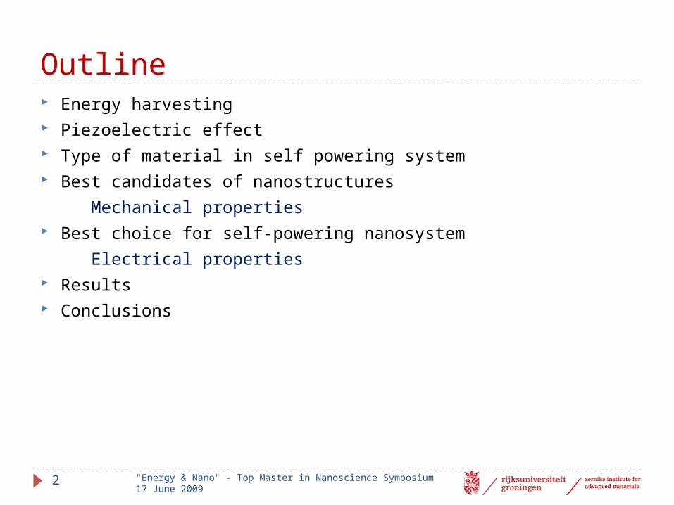
Outline Energy harvesting Piezoelectric effect Type of material in self powering system Best candidates of nanostructures
Mechanical properties Best choice for self-powering nanosystem
Electrical properties Results Conclusions
2 "Energy & Nano" - Top Master in Nanoscience Symposium 17 June 2009

Energy harvesting Definition:
Capturing and storing energy from available sources in environment which are currently wasting.
Applications:
In small and wireless autonomous devices (wearable electronics)
Types:
1- Photo/electrical energy harvesting
2- Thermal/electrical energy harvesting
3- Mechanical/electrical energy harvesting
3 "Energy & Nano" - Top Master in Nanoscience Symposium 17 June 2009
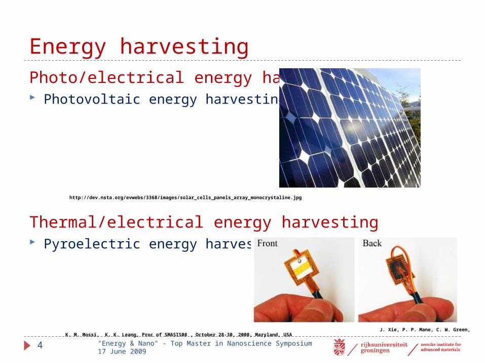
Energy harvestingPhoto/electrical energy harvesting Photovoltaic energy harvesting
Thermal/electrical energy harvesting Pyroelectric energy harvesting
4
http://dev.nsta.org/evwebs/3368/images/solar_cells_panels_array_monocrystaline.jpg
J. Xie, P. P. Mane, C. W. Green, K. M. Mossi, K. K. Leang, Proc of SMASIS08 , October 28-30, 2008, Maryland, USA
"Energy & Nano" - Top Master in Nanoscience Symposium 17 June 2009

Energy harvesting
5
M. Miyazaki,H.Tanaka,G.Ono,T.Nagano,N.Ohkubo,T.Kawahara,K.Yano, Proceedings of the 2003 international symposium on Low power electronics and design, Seoul, Korea,(2003),193
Biomechanical based energy harvesting
Electrostatic (capacitive) based energy harvesting
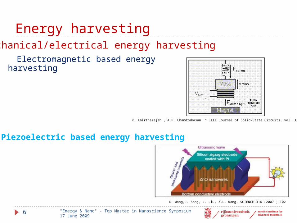
Mechanical/electrical energy harvesting
"Energy & Nano" - Top Master in Nanoscience Symposium 17 June 2009
Energy harvesting
6
X. Wang,J. Song, J. Liu, Z.L. Wang, SCIENCE,316 (2007 ) 102
R. Amirtharajah , A.P. Chandrakasan, " IEEE Journal of Solid-State Circuits, vol. 33, n. 5, pp. 687-695, 1998
Electromagnetic based energy harvesting
Piezoelectric based energy harvesting
Mechanical/electrical energy harvesting
"Energy & Nano" - Top Master in Nanoscience Symposium 17 June 2009
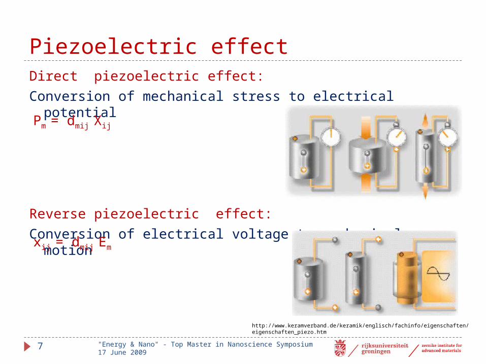
Piezoelectric effect Direct piezoelectric effect: Conversion of mechanical stress to electrical potential
Reverse piezoelectric effect: Conversion of electrical voltage to mechanical motion
7
http://www.keramverband.de/keramik/englisch/fachinfo/eigenschaften/eigenschaften_piezo.htm
"Energy & Nano" - Top Master in Nanoscience Symposium 17 June 2009
Pm = dmij Xij
xij = dmij Em

Piezoelectric materials
Insulator: Barium Sodium Niobate Lithium Niobate Lead Zirconate Titanate Quarts
Semiconductor: Cadmium Sulfide Gallium Arsenide Aluminum nitride (AIN) Polyvinylidene fluoride (PVDF) Zinc Sulfide
"Energy & Nano" - Top Master in Nanoscience Symposium 17 June 2009
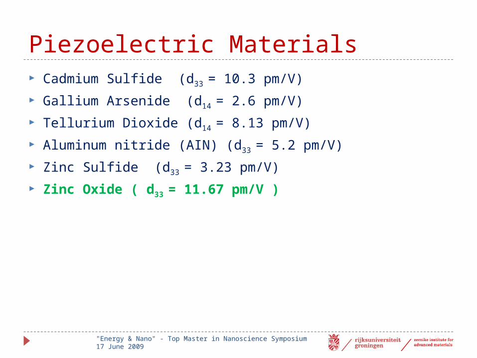
Piezoelectric Materials Cadmium Sulfide (d33 = 10.3 pm/V)
Gallium Arsenide (d14 = 2.6 pm/V)
Tellurium Dioxide (d14 = 8.13 pm/V)
Aluminum nitride (AIN) (d33 = 5.2 pm/V)
Zinc Sulfide (d33 = 3.23 pm/V)
Zinc Oxide ( d33 = 11.67 pm/V )
"Energy & Nano" - Top Master in Nanoscience Symposium 17 June 2009

Type of Materials ZnO as a piezoelectric energy harvesting material:
Lack of inversion center in wurtzite structure → strong piezoelectricity
Large electromechanical coupling
Semiconducting behaviour
More resistance to radiation
Biosafe with low toxicity (medical applications)
Large diversity of nanostructures
10
R. L. Johnson, Master Thesis, Iowa State University 2005
"Energy & Nano" - Top Master in Nanoscience Symposium 17 June 2009

Zinc Oxide Nanostructures Nanorods Nanobelts Hierarchical nanostructures
Nanocombs Nanosprings Nanorings
11
Z. L. Wang, Materialstoday(2004)26
"Energy & Nano" - Top Master in Nanoscience Symposium 17 June 2009

ZnO nanostructure for energy harvestingNanobelts /nanowires One dimensional structure Large elastic deformation without plastic deformation or fracture Free of dislocations because of their small diameter Bent under extremely small applied force.
Nanowire Nanobelt
12
Z. L. Wang, Materialstoday(2004)26
"Energy & Nano" - Top Master in Nanoscience Symposium 17 June 2009
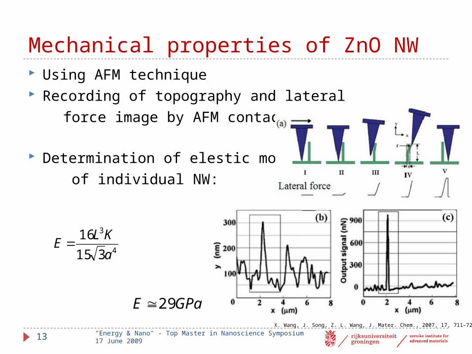
Mechanical properties of ZnO NW Using AFM technique Recording of topography and lateral
force image by AFM contact mode
Determination of elestic modulus
of individual NW:
13
GPaE 29
4
3
315
16
a
KLE
X. Wang, J. Song, Z. L. Wang, J. Mater. Chem., 2007, 17, 711–720
"Energy & Nano" - Top Master in Nanoscience Symposium 17 June 2009

Mechanical properties of ZnO NB Using TEM technique Sample holder for TEM to apply voltage across NB Induced mechanical resonance for applied frequency near natural
frequency of NB
14
xi
i
xT
LE
)4(3 2
2
yi
i
yW
LE
)4(3 2
2
GPaE 52Z.L. Wang/ Materials Science and Engineering R 64 (2009) 33–71
"Energy & Nano" - Top Master in Nanoscience Symposium 17 June 2009

Mechanical Modulus of ZnO NB/NW/Crystal Elastic modulus of individual NW :
Elastic modulus of individual NB :
Elastic modulus of ZnO crystal :
15
GPaE 29
GPaE 52
GPaE 140
"Energy & Nano" - Top Master in Nanoscience Symposium 17 June 2009

Preference of Nanowires versus Nanobelts
Lower range of Young modulus
Higher sensitivity to mechanical stress
More directionality
Easy to grow via chemical synthesis on any shaped substrate made of any material
16 "Energy & Nano" - Top Master in Nanoscience Symposium 17 June 2009

Electrical processes in Nanowires (NW) Coupling of piezoelectric and semiconducting properties of ZnO
nanowires:
1-Piezoelectric properties:
Charge Creation under mechanical stress
2-Semiconducting properties:
Low enough conductivity and carrier density for preserving the piezoelectric potential distribution in the NWs
High enough to transport the current under the driving of the piezoelectric potential energy
17 "Energy & Nano" - Top Master in Nanoscience Symposium 17 June 2009

Electrical processes in Nanowires (NW) Creation of strain field with NW Stretching of outer surface of NW
( positive strain) Compression of inner surface
(negative strain) Formation of electric field along the
NW in z direction ( ) ZnO NW acts as shottky diode
(forward and reverse biased)
18
dE zz /
Z. L. Wang, J. Song, SCIENCE, 312 (2006) 242
"Energy & Nano" - Top Master in Nanoscience Symposium 17 June 2009
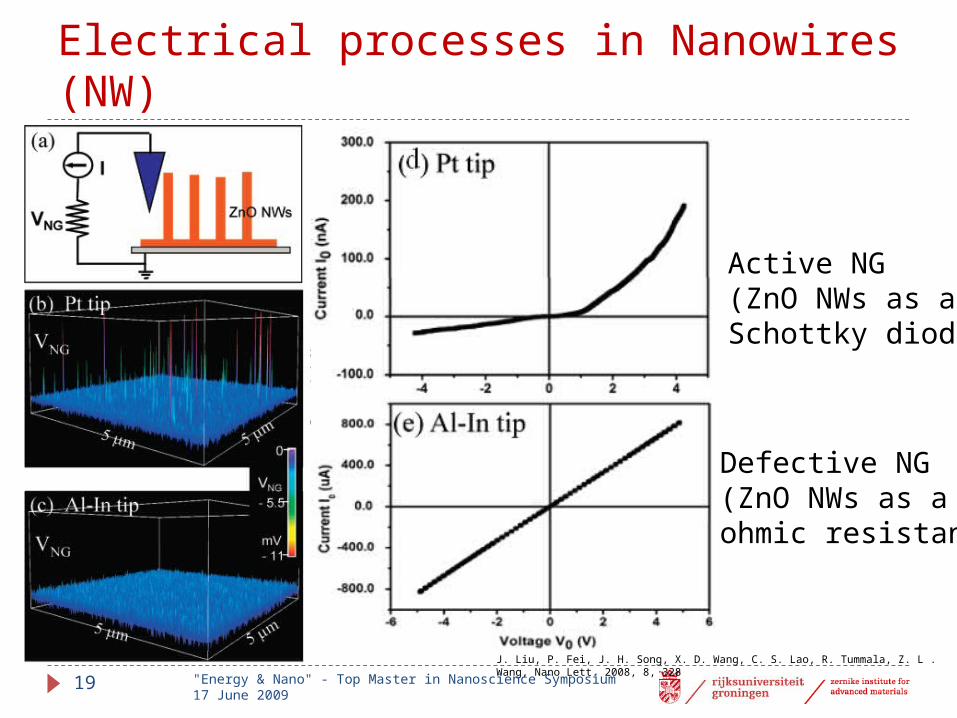
Electrical processes in Nanowires (NW)
19J. Liu, P. Fei, J. H. Song, X. D. Wang, C. S. Lao, R. Tummala, Z. L . Wang, Nano Lett. 2008, 8, 328
"Energy & Nano" - Top Master in Nanoscience Symposium 17 June 2009
Active NG (ZnO NWs as a Schottky diode)
Defective NG (ZnO NWs as aohmic resistance)

Results
AFM using Si tip coated with Pt
Using normal force in contact mode
20
Z. L. Wang, J. Song, SCIENCE, 312 (2006) 242
"Energy & Nano" - Top Master in Nanoscience Symposium 17 June 2009

Results Demonstration of ultra-sonic wave
transformation to electricity
21
X. Wang,J. Song, J. Liu, Z.L. Wang, SCIENCE,316 (2007 ) 102
"Energy & Nano" - Top Master in Nanoscience Symposium 17 June 2009

Conclusions
Importance of harvesting energy from available sources in environment.
Using of self-powering systems without changing battery Enhancement of harvesting efficiency in nanosystems Using ZnO as a suitable material for self-powering nanosystems Coupled semiconducting-piezoelectric properties of ZnO
nanostructure Nanowires /nanobelts are best candidate because of one-
dimensional & low Young Modulus and free of dislocation More alignment and lower Young modulus of NWs made it best
choice
22 "Energy & Nano" - Top Master in Nanoscience Symposium 17 June 2009

I would like to acknowledge Prof. B. Noheda for helping me to prepare this presentation.
23 "Energy & Nano" - Top Master in Nanoscience Symposium 17 June 2009

Thank you for your attention
Questions ?
24 "Energy & Nano" - Top Master in Nanoscience Symposium 17 June 2009