PIC-MINI-WEB development board
15
PIC-MINI-WEB development board Users Manual Rev. C, July 2006 Copyright(c) 2010, OLIMEX Ltd, All rights reserved Page 1
Transcript of PIC-MINI-WEB development board

PIC-MINI-WEB development board Users Manual
Rev. C, July 2006Copyright(c) 2010, OLIMEX Ltd, All rights reserved
Page 1
INTRODUCTION:
PIC-MINI-WEB is with dimensions only 55 x 36 mm but don't let this foolyou. This board is very powerful and will allow you to connect almosteverything to Internet.
The board has PIC18F25J10 microcontroller with 32KB of program Flashmemory, 1024 RAM memory and allows Microchip free TCP-IP stack to beprogrammed. In addition on-board flash of 1 Mbit (128KB) is available asdata storage for web pages and other data. The LAN connector could beconnected to 10 Mbit Ethernet switch or hub.
There is also IDC14 connector with 10 GPIOs available for future extensionand power supply and reset signals.
What CAN YOU do with this board? You name it: you can setup web serverwith dynamic web pages which allows you to read PIC resources or to drivethem through web interface, i.e. to read ADC and display it on the web orto toggle GPIO outputs from the web, very conveninet way to make homeautomation for instance and to monitor and control your home fromanywhere with Internet. Another service this board can run is FTP server,either you can control the PIC by Telnet, or you can send and receive e-mails and trigger hardware events with them. All this is possible due to thefree firmware which Microchip provides, and the best of all - it has neitherupfront charges for software nor royalies.
BOARD FEATURES:
− PIC18F25J10 microcontroller, ENC28J60 Ethernetcontroller, 32KB Flash, 1KB RAM
− 1Mbit on board serial flash for web pages storage− ICSP/ICD connector for programming and debugging
with PIC-ICD2, PIC-ICD2-POCKET and PIC-ICD2-TINY. − Reset button − User event button connected to RB0 interrupt − Complete web server and TCP-IP stack support as per
Microchip's open source TCP-IP stack − Power plug-in jack for +5VDC power supply − Voltage regulator +3.3V and filtering capacitors − Status LED − Extension header to connect to other boards, 10 GPIOs
and power supply, reset signals − Dimensions 55x36 mm (2.16x1.42")
ELECTROSTATIC WARNING:
The PIC-MINI-WEB board is shipped in protective anti-static packaging. Theboard must not be subject to high electrostatic potentials. General practicefor working with static sensitive devices should be applied when workingwith this board.
Page 2

BOARD USE REQUIREMENTS:
Cables: Depends on the used programming/debugging tool. It could be1.8 meter USB A-B cable to connect PIC-ICD2 or PIC-ICD2-POCKET to USB host on PC and RS232 cable, if you use PIC-ICD2-TINY. You will also need a LAN cable.
Hardware: Programmer/Debugger – some of Olimex programmers areapplicable, for example PIC-ICD2, PIC-ICD2-POCKET, PIC-ICD2-TINY or other compatible programming/debugging tool.
!!!Warning!!! When you want to program this microcontroller with PIC-ICD2, PIC-ICD2-POCKET or PIC-ICD2-TINY, before connectingthe programmer to your target board, you should first connectthe programmer to your computer and open MPLAB. There,first from menu Configure – Select Device – choose themicrocontroller you are about to program, then from menuProgrammer – Select Programmer – choose MPLAB ICD 2, waitwhile MPLAB is downloading operation system, and after ICD2is connected – check in menu Programmer – Settings – Power –there is option – Power target circuit from MPLAB ICD 2 – thisoption should be forbidden, you could not select it. Now it issafe to connect the programmer to your target board.
Software: PIC-MINI-WEB is tested with MPLAB IDE v.7.62 + MPLABC18 C compiler. It is possible that the stack might notfunction properly if used with later versions of MPLAB IDE.
PROCESSOR FEATURES:
PIC-MINI-WEB board uses MCU PIC18F25J10 from Microchip with thesefeatures:- Operating voltage range: 2.0V to 3.6V- 5.5V tolerant input (digital pins only)- On-chip 2.5V regulator- Low-power, high-speed CMOS Flash technology- C compiler optimized architecture:
o Optional extended instruction set designed to optimize re-entrant code
- Priority levels for interrupts- 8 x 8 Single-Cycle Hardware Multiplier- Extended Watchdog Timer (WDT)
o Programmable period from 4 ms to 131s- Single-Supply In-Circuit Serial Programming™ (ICSP™) via two pins- In-Circuit Debug (ICD) with three Break points via two pins- Power-Managed modes:
o Run: CPU on, peripherals ono Idle: CPU off, peripherals ono Sleep: CPU off, peripherals off
- Two Crystal modes, up to 40 MHz- Two External Clock modes, up to 40 MHz- Internal 31 kHz oscillator
Page 3

- Secondary oscillator using Timer1 @ 32 kHz- Two-Speed Oscillator Start-up- Fail-Safe Clock Monitor:
o Allows for safe shutdown if peripheral clock stops- High-current sink/source 25 mA/25 mA (PORTB and PORTC)- Three programmable external interrupts- Four input change interrupts- One Capture/Compare/PWM (CCP) module- One Enhanced Capture/Compare/PWM (ECCP) module:
o One, two or four PWM outputso Selectable polarityo Programmable dead timeo Auto-Shutdown and Auto-Restart
- Two Master Synchronous Serial Port (MSSP) modules supporting 3-wireSPI™ (all 4 modes) and I2C™ Master and Slave modes
- One Enhanced Addressable USART module:o Supports RS-485, RS-232 and LIN 1.2o Auto-Wake-up on Start bito Auto-Baud Detect
- 10-bit, up to 13-channel Analog-to-Digital Convertor module (A/D):o Auto-acquisition capabilityo Conversion available during Sleepo Self-calibration feature
- Dual analog comparators with input multiplexing
Page 4

BLOCK DIAGRAM:
Page 5

MEMORY MAP:
Page 6
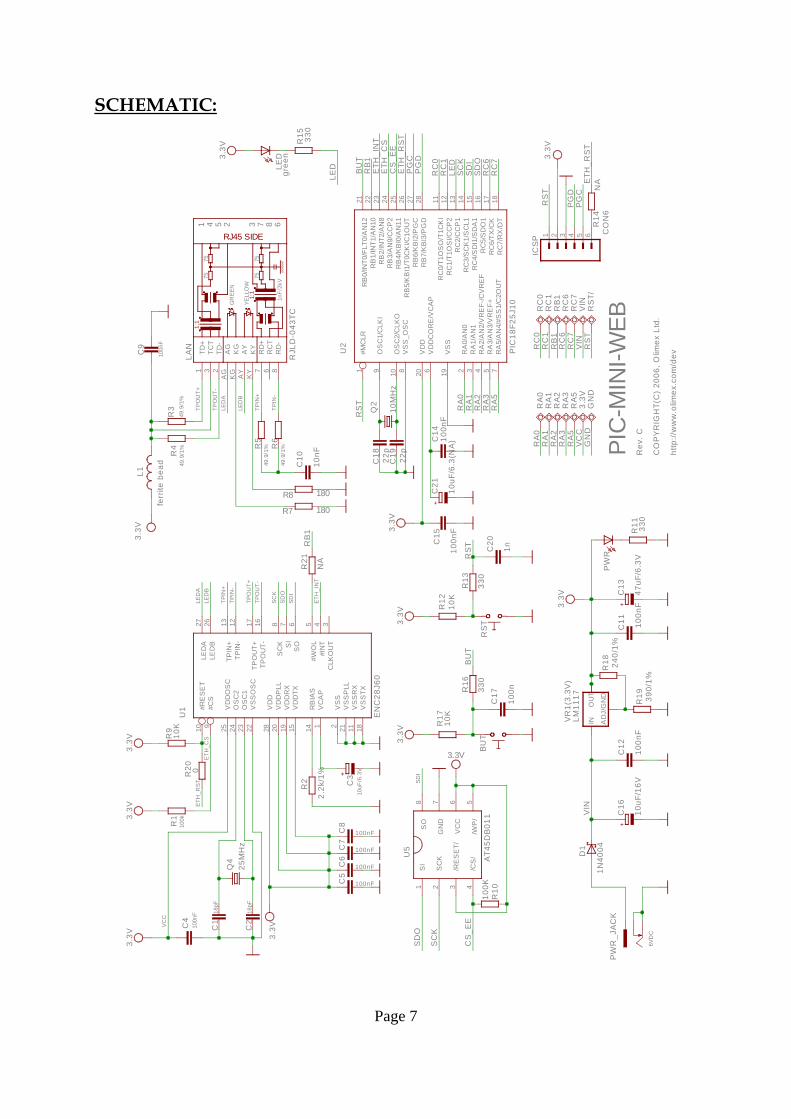
SCHEMATIC:
Page 7
18pF
18pF
10uF
/6.3
V
100n
F
100nF
100nF
100nF
100nF
100n
F
10nF
100n
F10
0nF
47uF
/6.3
V
100n
F10
0nF
10uF
/16V
100n
22p
22p
1n
10uF
/6.3
(NA
)
1N40
04C
ON
6
ferr
ite b
ead
RJL
D-0
43TC
gree
n
10M
Hz
25M
Hz
100k
2.2k
/1%
49.9
/1%
49.9
/1%
49.9
/1%
49.9
/1%
180
180
10K
100K
330
10K
330
NA
330
330
10K
240/
1%
390/
1%
0
NA
EN
C28
J60
PIC
18F2
5J10
AT4
5DB
011
3.3V
3.3V
3.3V
3.3V
3.3V
3.3V
3.3V
3.3V
3.3V
3.3V
3.3V
3.3V
LM11
17
BU
T
BU
T
CS
_EE
CS
_EE
ETH
_CS
ETH
_CS
ETH
_IN
T
ETH
_IN
T
ETH
_RS
T
ETH
_RS
T
ETH
_RST
GN
D
LED
LED
LED
A
LED
A
LED
B
LED
B
PG
C
PG
C
PG
D
PG
D
RA
0
RA
0
RA
1
RA
1
RA
2
RA
2
RA
3
RA
3
RA
5
RA
5
RB
1
RB
1
RB
1
RC
0
RC
0
RC
1
RC
1
RC
6
RC
6
RC
7
RC
7
RS
T
RS
T
RS
T
RS
T
SCK
SC
K
SC
K
SD
I
SDI
SDI
SD
O
SDO
SD
O
TPIN
+
TPIN
+
TPIN
-
TPIN
-
TPO
UT+
TPO
UT+
TPO
UT-
TPO
UT-
VCC
VC
CV
INV
IN3.
3V
BU
T
C1
C2
C3
C4
C5
C6
C7
C8
C9
C10
C11
C12
C13
C14
C15
C16
C17
C18
C19
C20
C21
D1
GN
D
1 2 3 4 5 6
ICS
P
L1
AG
AG
AY
AY
KG
KG
KY
KY
RC
T6
RD
+7
RD
-8
TCT
3TD
+1
TD-
275
75
7575
1nF/
2kV
1 4 5 2 3 7 8 6
GR
EEN
YELL
OW
LAN
LED
PW
RP
WR
_JA
CK
Q2
Q4
R1
R2
R3
R4 R
5
R6
R7
R8
R9
R10
R11
R12
R13
R14
R15
R16
R17
R18
R19
R20
R21
RA
0R
A1
RA
2R
A3
RA
5
RB
1
RC
0R
C1
RC
6R
C7
RS
T
RS
T/
#CS
9
#IN
T4
#RE
SE
T10
#WO
L5
CLK
OU
T3
LED
A27
LED
B26
OS
C1
23O
SC
224
RB
IAS
14
SC
K8
SI
7
SO
6
TPIN
+13
TPIN
-12
TPO
UT+
17
TPO
UT-
16
VC
AP
1
VD
D28
VD
DO
SC
25
VD
DP
LL20
VD
DR
X19
VD
DTX
15
VS
S2
VS
SO
SC
22
VS
SP
LL21
VS
SR
X11
VS
STX
18
U1
#MC
LR1
OS
C1/
CLK
I9
OS
C2/
CLK
O10
RA
0/A
N0
2
RA
1/A
N1
3
RA
2/A
N2/
VR
EF-
/CV
RE
F4
RA
3/A
N3/
VR
EF+
5
RA
5/A
N4/
#SS
1/C
2OU
T7
RB
0/IN
T0/F
LT0/
AN
1221
RB
1/IN
T1/A
N10
22
RB
2/IN
T2/A
N8
23
RB
3/A
N9/
CC
P2
24
RB
4/K
BI0
/AN
1125
RB
5/K
BI1
/T0C
KI/C
1OU
T26
RB
6/K
BI2
/PG
C27
RB
7/K
BI3
/PG
D28
RC
0/T1
OS
O/T
1CK
I11
RC
1/T1
OS
I/CC
P2
12
RC
2/C
CP
113
RC
3/S
CK
1/S
CL1
14
RC
4/S
DI1
/SD
A1
15
RC
5/S
DO
116
RC
6/TX
/CK
17
RC
7/R
X/D
T18
VD
D20
VD
DC
OR
E/V
CA
P6
VS
S19
VS
S_O
SC
8
U2
/CS
/4
/RE
SE
T/3
/WP
/5
GN
D7
SC
K2
SI
1S
O8
VC
C6
U5
VIN
AD
J/G
ND
INO
UT
VR
1(3.
3V)
6VD
C
PIC
-MIN
I-WEB
Rev
. C
CO
PY
RIG
HT(
C)
2006
, Olim
ex L
td.
http
://w
ww
.olim
ex.c
om/d
ev
+
+
+
+
RJ45 SIDE
1:1
1:1

BOARD LAYOUT:
POWER SUPPLY CIRCUIT:
PIC-MINI-WEB takes power from PWR_JACK where 6-9 VDC is applied byexternal power source
The board power consumption is: about 180 mA with all peripherals andMCU running at full speed.
RESET CIRCUIT:
PIC-MINI-WEB reset circuit is made with R12 (10k) pull-up, R13 (330Ω)and capacitor C20 (100nF) and RST button. Manual reset is possible by the RST button.
CLOCK CIRCUIT:
Quartz crystal 10 MHz is connected to PIC18F25J10 pin 9 clock in(OSC1/CLKIN) and pin 10 clock out (OSC2/CLKOUT).
JUMPER DESCRIPTION:
There aren’t any jumpers.
Page 8

INPUT/OUTPUT:
One User button with name BUTTON – connected to PIC18F25J10 pin 21(PORTB.RB0/INT0/FLT0/AN12);
Status green LED connected to PIC18F25J10 pin13 (PORTC.RC2/CCP1).
Power supply red LED with name PWR – indicates that external powerssource is applied and board power supply is applied;
EXTERNAL CONNECTORS DESCRIPTION:
ICSP:
Pin # Signal Name
1 RST
2 +5V
3 GND
4 PGD
5 PGC
6 PGM
PGD I/O Program Data. Serial data for programming.PGC Input Program Clock. Clock used for transferring the serial data (output fromICSP, input for the MCU).
PWR_JACK:
Pin # Signal Name
1 Power Input
2 GND
The power input should be +(6 - 9)VDC.
Page 9

EXT :
Pin # Signal Name Pin # Signal Name
1 RA0/AN0 2 RC0/T1OSO/T1CKI
3 RA1/AN1 4 RC1/T1OSI/CCP2
5 RA2/AN2/VREF-/CVREF 6 RB1/INT1/AN10
7 RA3/AN3/VREF+ 8 RC6/TX/CK
9 RA5/AN4/#SS1/C2OUT 10 RC7/RX/DT
11 VCC +3.3 V 12 VIN
13 GND 14 RST/
LAN:
Pin # Signal Name Chip Side Pin # Signal Name Chip Side
1 TPOUT+ 5 Not Connected (NC)
2 TPOUT- 6 Not Connected (NC)
3 3.3V 7 TPIN+
4 Not Connected (NC) 8 TPIN-
Page 10

LED Color Usage
Right Yellow Activity
Left Green 100MBits/s (Half/Full duplex)
TPOUT- Output Differential signal output.TPOUT+ Output Differential signal output. TPIN- Input Differential signal input.TPIN+ Input Differential signal input.
Page 11
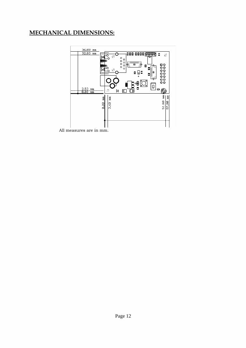
MECHANICAL DIMENSIONS:
All measures are in mm.
Page 12

AVAILABLE DEMO SOFTWARE :
You could find information about PIC-MINI-WEB board, Microchip TCP/IPstack and how to change and configure the software in Understanding PIC-WEBboards on www.olimex.com/dev .
Page 13
ORDER CODE:
PIC-MINI-WEB – assembled and tested (no kit, no soldering required)
How to order? You can order to us directly or by any of our distributors. Check our web www.olimex.com/dev for more info.
All boards produced by Olimex are RoHS compliant
Revision history:
REV. C - created July 2006
Page 14
Disclaimer: © 2010 Olimex Ltd. All rights reserved. Olimex®, logo and combinations thereof, areregistered trademarks of Olimex Ltd. Other terms and product names may be trademarks ofothers.The information in this document is provided in connection with Olimex products. Nolicense, express or implied or otherwise, to any intellectual property right is granted by thisdocument or in connection with the sale of Olimex products. Neither the whole nor any part of the information contained in or the product described inthis document may be adapted or reproduced in any material from except with the priorwritten permission of the copyright holder.The product described in this document is subject to continuous development andimprovements. All particulars of the product and its use contained in this document aregiven by OLIMEX in good faith. However all warranties implied or expressed including butnot limited to implied warranties of merchantability or fitness for purpose are excluded.This document is intended only to assist the reader in the use of the product. OLIMEX Ltd.shall not be liable for any loss or damage arising from the use of any information in thisdocument or any error or omission in such information or any incorrect use of the product.
Page 15