
PIC Microcontroller and E b dd d S tEmbedded...
78
PIC Microcontroller and E b dd d S t Embedded Systems Muhammad Ali Mazidi, Rolin McKinlay and Danny Causey Eng. Husam Alzaq The Islamic Uni. Of Gaza The PIC uCs 1-1
Transcript of PIC Microcontroller and E b dd d S tEmbedded...

PIC Microcontroller and E b dd d S tEmbedded Systems
Muhammad Ali Mazidi, Rolin McKinlay and Danny Causey
Eng. Husam AlzaqE g m qThe Islamic Uni. Of Gaza
The PIC uCs 1-1

Chapter 2:pPIC Architecture And A bl L Assembly Language Programming Programming.
The WREG Register
PIC Microcontroller d E b dd d S
The PIC File RegisterUsing instruction with the default
and Embedded SystemsMuhammad Ali Mazidi, Rolin McKinlay and D C s F b
access bank
Danny Causey, February 2007.
The PIC uCs 1-2

OutlineOutline
P PIC Status RegisterPIC data format and directiveIntro. To PIC assembly languageAssembling and linking a PIC programAssembling and linking a PIC programThe Program Counter and program ROM space in the PICspace in the PICRISC Architecture in the PICViewing Register and memory with MPLAB simulator
The PIC uCs 1-3

ObjectiveObjective
E h d f l f h P Examine the data RAM fileReg of the PIC uCManipulate data using the WREG & MOVEp gPerform simple operations such ADD and fileReg using and access bank in the PIC uCfileReg using and access bank in the PIC uCExplain the purpose of the status regDiscuss data RAM memory space allocation in Discuss data RAM memory space allocation in the PIC uCLi SFR f h PIC CList SFRs of the PIC uCDescribe PIC data types and directives
The PIC uCs 1-4

The WREG RegisterThe WREG Register
M i f i h i d l i Many registers for arithmetic and logic operation.The WREG (WORking Register) Register is one of the most widely used registers of y gthe PIC
8-bit register any data larger than 8 bits g y gmust be broken into 8-bits chunks before it is processed.There is only one .D7 D6 D5 D2D4 D3 D1 D0
The PIC uCs 3-5

MOVLWMOVLW
b d EGMoves 8-bit data into WREGMOVLW k; move literal value k into WREG
ExampleMOVLW 25HMOVLW A5H
Is the following code correct?MOVLW 9HMOVLW 9HMOVLW A23H
The PIC uCs 1-6

ADDLWADDLW
DDLW k dd li l l k WREG (k WREG)ADDLW k; Add literal value k to WREG (k +WREG)
0 0 0 01 0 1 0Example:MOVLW 12H ;ADDLW 16H ;
0 0 0 01 0 1 0
0 0 1 00 1 0 0ADDLW 16H ;ADDKW 11H ;ADDLW 43H ;
0 0 1 00 1 0 0
0 0 1 01 1 0 1ADDLW 43H ; 0 0 1 01 1 0 1
0 1 1 11 1 0 00 1 1 11 1 0 0
The PIC uCs 1-7

Figure 2-1. PIC WREG and ALU Using Literal Value
The PIC uCs 1-8
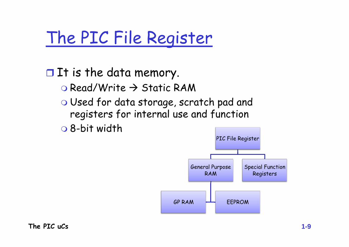
The PIC File RegisterThe PIC File Register
h d It is the data memory.Read/Write Static RAMUsed for data storage, scratch pad and registers for internal use and function8-bit width
PIC File Register
General Purpose RAM
Special Function Registers
GP RAM EEPROM
The PIC uCs 1-9

Register File ConceptRegister File ConceptRegister File Concept: All of data
Data Memory(Register File)
Concept: All of data memory is part of the register file, so any location in data
w fALU
07h
08h
09h
Dat
a B
us
d
any location in data memory may be operated on directly
w f
0Ah
0Bh
0Ch
D directlyAll peripherals are mapped into data
0Dh
0Eh
0Fh
10h memory as a series of registersOrthogonal
WREG10h
Decoded Instruction from Program Memory:
gInstruction Set: ALL instructions can operate on ANY
Opcode d a Address
The PIC uCsThe PIC uCs
Arithmetic/Logic Function to be Performed Result
Destination
Address of Second Source Operand
pdata memory location 1-10

PIC18F Programming ModelPIC18F Programming Model
The PIC uCs 1-11

Special Function RegistersSpecial Function Registers
d d d f f h dedicated to specific functions such as ALU status, timers, serial communication, / DI/O ports, ADC,…
The function of each SFR is fixed by the yCPU designer at the time of design
it is used for control of the microcontroller or peripheral
8-bit registersgTheir numbers varies from one chip to another
The PIC uCs
another.1-12

General Purpose RAMGeneral Purpose RAM
G f lGroup of RAM locations8-bit registersgLarger than SFR
Difficult to manage them by using Assembly Difficult to manage them by using Assembly languageEasier to handle them by C Compiler.y p
The microchip website provides the data The microchip website provides the data RAM size, which is the same as GPR size.
The PIC uCs 1-13

File Register Size File Register Size
File Register=
SFR+
GPR= +
(Bytes) (Bytes) (Bytes)PIC12F508 32 7 25PIC12F508 32 7 25PIC16F84 80 12 68PIC18F1220 512 256 256PIC18F1220 512 256 256PIC18F452 1792 256 1536PIC18F2220 768 256 512PIC18F458 1792 256 1536PIC18F8722 4096 158 3938
The PIC uCsPIC18F4550 2048 160 1888
1-14

Figure 2-2. File Registers of PIC12, PIC16, and PIC18
The PIC uCs 1-15

The PIC uCs 1-16

GPRAM VS EEPROMGPRAM VS. EEPROM
dd An add-on memoryCan be zero size
The PIC uCs 1-17

File Register and access bank in the PIC18
h P 1 F l h f 40 6 The PIC18 Family can have a max. of 4096 Bytes.The File Register
has addresses of 000- FFFHdivided into 256-byte banksMax. 16 banks (How?)( )
At least there is one bankKnown as default access bankKnown as default access bank.
Bank switching is a method used to access all the banks
The PIC uCs
all the banks1-18

Figure 2-3. File Register for PIC18 Family
The PIC uCs 1-19

Access bank in the PIC18Access bank in the PIC18
6 B b kIt is 256-Byte bank.Divided into equal two discontinuous qsections (each 128 B).
GP RAM, from 0 to 7FHSFR, from F80H to FFFH
The PIC uCs 1-20

Figure 2-4. SFRs of the PIC18 Family.
The PIC uCs 1-21

Using instruction with the default access bank
d h We need instruction to access other locations in the file register for ALU and
h other operations.MOVWFCOMFDECFMOVFMOVFF
The PIC uCs 1-22

MOVWF instructionMOVWF instruction
F d f f l F indicates for a file registerMOVWF Address
It tells the CPU to copy the source register, WREG, to a destination in the file register, WREG, to a destination in the file register.
A location in the SPRA location in the SPRA location in GP RAM
WREG
The PIC uCs 1-23

Example 2-1Example 2-1
MOVLW 99H 99 Add D t
WRFG
MOVLW 99H MOVWF 12H
99 Address Data012H013H85MOVLW 85H
MOVWF 13H014H015H016H3F
85
MOVLW 3FH MOVWF 14H
016H3FAddress Data
MOVLW 63H MOVWF 15H
63 012H 99013H 85014H 3F
MOVLW 12H MOVWF 16H
12014H 3F015H 63016H 12
The PIC uCs 1-24

NoteNote
l l l d l We cannot move literal values directly into the general purpose RAM location in the P 18 h b d h PIC18. They must be moved there via WREG.
The PIC uCs 1-25

ADDWFADDWF
dd h h f EG d Adds together the content of WREG and a file register location
ADDWF File Reg. Address, DThe result will be placed in either the The result will be placed in either the WREG or in the file register location
D indicates the destination bitD indicates the destination bitIf D=0 or (D=w)
The result will be placed in the WREGThe result will be placed in the WREGIf D=1 or (D=f)
Th l ill b l d i h fil iThe PIC uCs
The result will be placed in the file register1-26

Example 2-2Example 2-2
h f f l l State the content of file register location and WREG after the following program
MOVLW 0 MOVWF 12H 0 Address Data
012H 0
Address Data012H 22Address Data012H 44Address Data012H 66
Address Data012H 88MOVWF 12H
MOVLW 22H ADDWF 12H F
012H 0013H014H
22 013H014H015H
012H 44013H014H
012H 66013H014H013H014H015HADDWF 12H, F
ADDWF 12H, F015H016H
015H016H015H016H015H016H015H016H
ADDWF 12H, FADDWF 12H, F
The PIC uCs
DDWF H, F
1-27

Example 2-3Example 2-3
h f f l l State the content of file register location and WREG after the following program
MOVLW 0 MOVWF 12H 0 Address Data
012H 0Address Data012H 22MOVWF 12H
MOVLW 22H ADDWF 12H F
013H014H015H
22012H 22013H014H
ADDWF 12H, FADDWF 12H, W
015H016H015H016H44
ADDWF 12H, WADDWF 12H, W
6688
The PIC uCs
DDWF H, W
1-28
88

Figure 2-5. WREG, fileReg, and ALU in PIC18
The PIC uCs 1-29

COMF instructionCOMF instruction
F F l dd DCOMF File Reg. Address, DIt tells the CPU to complement the content pof fileReg and places the results in WREG or in fileReg.g
The PIC uCs 1-30

Example 2-4Example 2-4
l l h F Write a simple program to toggle the SFR of Port B continuously forever.
SolutionMOVLW 55H
55 Address DataF81H 55HAddress Data
MOVLW 55HMOVWF PORTB
B1 F P B F
F81H 55HF82HF83H
F81H AAHF82HF83H
B1 COMF PORTB, FGOTO B1
F83H
The PIC uCs 1-31

DECF instructionDECF instruction
DE F F l dd DDECF File Reg. Address, DIt tells the CPU to decrement the content of fileReg and places the results in WREG or in fileReg.
3 Address DataAddress Datag
Example:MOVLW 3
3 Address Data012H 3013H
Address Data012H 2013HMOVLW 3
MOVWF 20HDECF 20H F
014H015H016H
014H015H016HDECF 20H, F
DECF 20H, FDECF 20H F
016H016H
The PIC uCs
DECF 20H, F
1-32

DECF instructionDECF instruction
DE F F l dd DDECF File Reg. Address, DIt tells the CPU to decrement the content of fileReg and places the results in WREG or in fileReg.
3 Address DatagExample:
MOVLW 3
3 Address Data012H 3013H2MOVLW 3
MOVWF 20HDECF 20H w
014H015H016H
1DECF 20H, wDECF 20H, wDECF 20H w
016H
0
The PIC uCs
DECF 20H, w
1-33

MOVF instructionMOVF instruction
F F l dd DMOVF File Reg. Address, DIt is intended to perform MOVFWp
MOVFW isn’t existedIf D=0If D 0
Copies the content of fileReg (from I/O pin) to WREG
If D=1The content of the fileReg is copied to itself The content of the fileReg is copied to itself. (why?)
The PIC uCs 1-34

MOVF instructionMOVF instruction
F F l dd 0MOVF File Reg. Address, 0
WREG
The PIC uCs 1-35
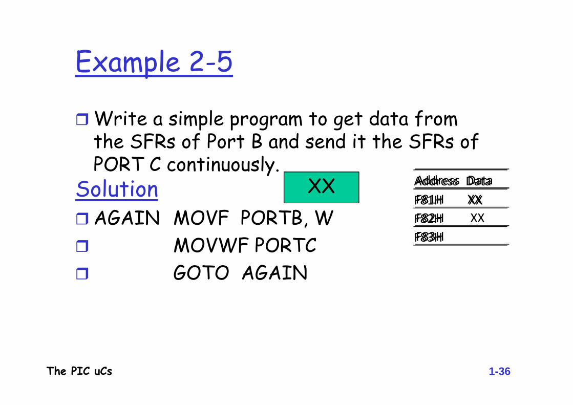
Example 2-5Example 2-5
l d f Write a simple program to get data from the SFRs of Port B and send it the SFRs of P R lPORT C continuously.
Solution XX Address DataF81H XX
Address DataF81H XX
AGAIN MOVF PORTB, WMOVWF PORTC
F81H XXF82HF83H
F81H XXF82H XXF83HMOVWF PORTC
GOTO AGAIN
The PIC uCs 1-36

Example 2-6Example 2-6
l d f Write a simple program to get data from the SFRs of Port B Add the value 5 to it
d d h FR f P R and send it the SFRs of PORT C Solution 55
Address DataF81H 55H
Address DataF81H 55H5A
MOVF PORTB,WADDLW 05H
55 F81H 55HF82HF83H
F81H 55HF82H 5AHF83H
5A
ADDLW 05HMOVWF PORTC
The PIC uCs 1-37

MOVFF instructionMOVFF instruction
d f l F lIt copies data from one location in FileRegto another location in FileReg.
MOVFF Source FileReg, destination FileReg
The PIC uCs 1-38

Example 2-7Example 2-7
l d f Write a simple program to get data from the SFRs of Port B and send it the SFRs of P R lPORT C continuously.
Solution XX Address DataF81H XXAddress DataF81H XX
AGAIN MOVFF PORTB, PORTCGOTO AGAIN
F81H XXF82HF83H
F81H XXF82H XXF83H
GOTO AGAIN
The PIC uCs 1-39

PIC Status RegisterPIC Status Register
d h d To indicate arithmetic conditions It is a 8-bit registerg
Five bits are usedD0: C Carry FlagD0 C Carry FlagD1: DC Digital Carry FlagD2: Z Z FlD2: Z Zero FlagD3: OV Overflow FlagD4: N Negative Flag
The PIC uCs 1-40

Figure 2-7 Bits of Status RegisterFigure 2 7. Bits of Status Register
The PIC uCs 1-41

Example 2-8Example 2-8
h h f h D fl f Show the status of the C, DC, Z flags after the following addition instruction
MOVLW 38HADDLW 2FHADDLW 2FH
Solution38H + 2FH 67H WREG 67H38H + 2FH = 67H WREG=67H
C=0DC 1DC=1Z=0
The PIC uCs 1-42

Example 2-9Example 2-9
h h f h D fl Show the status of the C, DC, Z flags after the following addition instruction
MOVLW 9CHADDLW 64HADDLW 64H
Solution9CH + 64H 100H WREG 00H9CH + 64H = 100H WREG= 00H
C=1DC 1DC=1Z=1
The PIC uCs 1-43

Instruction That Affect Flag Bits
The PIC uCs 1-44

Instruction That Affect Flag Bits
The PIC uCs 1-45

Instruction That Affect Flag Bits
The PIC uCs 1-46

Flag Bits and Decision MakingFlag Bits and Decision Making
The PIC uCs 1-47

PIC Data Format and DirectivesPIC Data Format and Directives
h d There is one data type8 bitsIt is the job of the programmer to break down data larger 8 bits
Data type can be positive or negativeData format are
Hex (default in PIC) 12 or 0x12 or H'12' or 12HBinary B'00010010' B nary B 000 00 0 Decimal .12 or D'12' ASCII A'c' or a'c'
The PIC uCs
ASCII A c or a c
1-48

Assembler Directives Assembler Directives
h h d ff b What is the difference between Instruction and Directives?EQU
Defines a constant or fixed addressSET
Defines a constant or fixed addressDefines a constant or fixed addressMaybe reassigned later
ORG (Origin)ORG (Origin)END
The PIC uCsLIST
1-49

Rules for labels in A LRules for labels in A.L.
Unique nameAlphabetic lettersp
Upper, lower, digits (0-9),special char. (? . @_ $)
The first letter must be Alphabetic lettersNot a reserved wordNot a reserved word
The PIC uCs 1-50

Introduction to PIC Assembly Language
D ff l f d l h h h Difficult for us to deal with the machine code ( 0s and 1s)Assembly Language provide
Mnemonic: codes and abbreviations that are easy to remember Faster programming and less prone errorLLL (why?)Programmer must know all Reg. …etc.
Assembler is used to translate the assembly code into machine code (object
The PIC uCs
m y m ( jcode)
1-51

Structure of Assembly Language
f lSeries of linesInstructionDirectives
Consists of four field[label] mnemonic [operands] [;commands]
Label: refer to line by code (certain length)Label: refer to line by code (certain length)Mnemonic and operands are task that sh ld b t dshould be executed.
Directive don’t generate any machine code and used by assembler
The PIC uCs
used by assembler 1-52

Sample of Assembly Language Program
UM EQU 10H R M l 10H f UMSUM EQU 10H ;RAM loc 10H fro SUMORG 0H; start at address 0MOVLW 25H ; WREG = 25ADDLW 0x34 ;add 34H to WREG=59HADDLW 11H ;add 11H to WREG=6AHADDLW D’18’ ; W = W+12H=7CHADDLW 1CH ; W = W+1CH=98HADDLW b’00000110’ ; W = W+6H=9EHMOVWF SUM ;save the result in SUM location
HERE GOTO HERE ;stay here forever
The PIC uCsEND ; end of asm source file
1-53

Assembling and Linking A PIC Program
Figure 2Figure 2-8. Steps
C to Create a Programg
The PIC uCs 1-54

List FileList File
The PIC uCs 1-55

The Program Counter and Program ROM Space in the PIC
P (P ) d b h P Program Counter (PC) is used by the CPU to point to the address of the next
b dinstruction to be executedThe wider the program counter, more the p gmemory locations can be accessed
PIC16 has 14 bits (8K)( )PIC18 has 21 bits (2M)8051 has 16 bits (64K)( )
The PIC uCs 1-56

Figure 2-9. Program Counter in PIC18
The PIC uCs 1-57

The PIC uCs 3-58

Example 2-11Example 2 11
F d h dd f h f Find the ROM Memory Address of each of the following PIC chips:
a) PIC18F2220b) PIC18F2410b) PIC18F2410c) PIC18F458
The PIC uCs 1-59

P i UPAt what address does the
Powering UPAt what address does the CPU wake up when power applied?applied?• The uC wakes up at
mem r address 0000memory address 0000• The PC has the value 0000• ORG directive put the
address of the first op pcode at the memory location 0000
The PIC uCs 1-60
Figure 2-11. PIC18 Program ROM Space

Placing Code in program ROMPlacing Code in program ROM
The PIC uCs 1-61

Program MemoryProgram Memory
All instructions are 2Byte All instructions are 2Byte except the GOTO, which has 4-Byte
The PIC uCs 1-62

Program ROM Width for the PIC18
B dd bl h l h ld l Byte addressable: each location holds only one byte
CPU with 8-Bit will fetch one byte a timeIncreasing the data bus will bring more information
Solution: Data bus between CPU and ROM can be similar to traffic lanes on the highwayg yThe wide of Data path is 16 bit
Increase the processing powerIncrease the processing powerMatch the PIC18 instruction single
cycle
The PIC uCs
cycle
1-63

Figure 2-12. Program ROM Width for the PIC18
The PIC uCs 1-64

Little endian VS big endian warLittle endian VS big endian war
h l b h l The low byte goes to the low memory locationThe high byte goes to the high memory locationIntel uP and many uCs use little endian
The PIC uCs 1-65

Figure 2-13. PIC18 Program ROM Contents for Program 2-1 List File
The PIC uCs 1-66

Harvard Architecture in the PIC
N h h Von Neumann Architecture: uses the same bus for accessing both the code and data memory.
Slow down the processing speedGet in each other’s way
Harvard Architecture: uses separate buses pfor accessing the code and data memory.
Inexpensive for a chipp p
The PIC uCs 1-67

Figure 2-14. von Neumann vs. Harvard Architecture
The PIC uCs 1-68

Instruction size of the PIC18Instruction size of the PIC18
P B 4 BPIC Instructions are 2-Byte or 4-ByteThe first seven or eight bits represents g pthe op-codeMost of PIC18 instructions are 2-ByteMost of PIC18 instructions are 2 Byte
MOVLW 0000 1110 kkkk kkkk (0E XX)ADDLW 0000 1111 kkkk kkkk (0F XX)ADDLW 0000 1111 kkkk kkkk (0F XX)MOVWF 0110 111a ffff ffff (6E XX
or 6F XX)F )• A specifies the default access bank if it is 0 and if a
= 1 we have to use bank switching
The PIC uCs 1-69

Instruction size of the PIC18Instruction size of the PIC18
4 B l d 4-Byte instructions include MOVFF (move data within RAM, which is 4k)
• 1100 ssss ssss ssss (0≤ fs ≤ FFF)• 1111 dddd dddd dddd (0≤ fd ≤ FFF)
GOTO (th d dd b idth i 21 hi h GOTO (the code address bus width is 21, which is 2M)
• 1110 1111 k kkk kkkk01110 1111 k7kkk kkkk0
• 1111 k19kkk kkkk kkkk8
The PIC uCs 1-70

RISC Architecture in the PICRISC Architecture in the PIC
h f h To increase the processing power of the CPU1. Increase the clock frequency of the chip2. Use Harvard architecture 3. change the internal architecture of the CPU
and use what is called RISC architecture
The PIC uCs 1-71

RISC Architecture in the PICRISC Architecture in the PIC
RISCSimple and Small
CISCComplex and large p
instruction setRegular and fixed
p ginstruction setIrregular instruction Regular and fixed
instruction formatSimple address
Irregular instruction formatComplex address Simple address
modesPipelined instruction
Complex address modesMay also pipeline Pipelined instruction
execution --> 95% executed in one cycle
May also pipeline instruction execution
The PIC uCs
executed in one cycle 1-72

RISC Architecture in the PICRISC Architecture in the PIC
RISCProvide large number
CISCProvide smaller number g
of CPU registersSeparated data and
of CPU registersCombined data and Separated data and
program memoryMost operations are
Combined data and program memoryMost operations can be Most operations are
register to registerTake shorter time to
Most operations can be register to memoryTake longer time to Take shorter time to
design and debugTake longer time to design and debug
The PIC uCs 1-73

Viewing Register and memory with MPLAB Simulater
The PIC uCs 1-74

Figure 2-15. SFR Window in MPLAB Simulator
The PIC uCs 1-75

Figure 2-16. File Register (Data RAM) Window in MPLAB Simulator
The PIC uCs 1-76

Figure 2-17. Program (Code) ROM Window in MPLAB ROM Window in MPLAB Simulator
The PIC uCs 1-77

Chapter 2: SummaryChapter 2: SummarySample PIC18 Sample PIC18 Instructions
Move add subtractMove, add, subtract
Next:Branch, Call and Time ,
Delay Loo
The PIC uCs 3-78


![Copyright © 2007 Pearson Education, Inc. Publishing as ...site.iugaza.edu.ps/hzaq/files/2010/02/DB_Ch05.pdfTitle Microsoft PowerPoint - DB Ch05 [Compatibility Mode] Author hzaq Created](https://static.fdocuments.net/doc/165x107/60a2765cfe9f4742f8327b57/copyright-2007-pearson-education-inc-publishing-as-site-title-microsoft.jpg)


