Physics Challenges Facing the Semiconductor Industry · PDF filePhysics Challenges Facing the...
68
Physics Challenges Physics Challenges Facing the Facing the Semiconductor Industry Semiconductor Industry Based on the Based on the Alain C. Diebold
Transcript of Physics Challenges Facing the Semiconductor Industry · PDF filePhysics Challenges Facing the...

Physics Challenges Physics Challenges
Facing the Facing the
Semiconductor IndustrySemiconductor Industry
Based on theBased on the
Alain C. Diebold
AcknowledgementsAcknowledgements• PY Hung, Hugo Celio, Jimmy Price
• Mark Bohr Intel
• Novjot Chhabra and Ken Monnig
• ITRS Metrology US and International TWGs
• References– International Technology Roadmap for Semiconductors– HJ Levinson, Principles of Lithography– C Steinbruchel and BL Chin - Copper Interconnect Technology– SM Sze – High Speed Semiconductor Devices– How CMOS works
http://tech-www.informatik.uni-hamburg.de/applets/cmos/cmosdemo.html– Fabrication Process
http://jas.eng.buffalo.edu/education/fab/invFab/

AGENDAAGENDA
• The ITRS Challenge
• Litho Processes and Metrology
• FEP Processes and Metrology
• Interconnect Processes and Metrology
• Materials Characterization

TerminologyTerminology 0.065 µm High-performance Micro- Processor
pitch = distance between closest spaced metal interconnect lines at first level of DRAM
Pitc
h
Transistor
source drainGate
Side ViewTopView
CDCD
Figure courtesy Bryan Tracy

CMOSCMOS InverterComplementary Metal Oxide Semiconductor Field Effect Transistor
P Channel Transistor - Carriers = holes
N Channel Transistor – Carriers = electrons
Vin Vout
VDD – voltage supply
Digital -- 0 and 1At Vin = 0, Vout/VDD = 1 As input voltage Vin goes from 0 to 1 = Vin/VDD Vout/VDD = 1

CMOSCMOSSwitching Speed ττττ ~ 1/Idsatgoverned by Saturation Drive Current
P Channel Transistor - Carriers = holes
N Channel Transistor – Carriers = electrons
Vin Vout
VDD – voltage supply
Idsat

CMOSCMOSWhat it looks like
http://jas.eng.buffalo.edu/education/fab/invFab/See the process in action

TerminologyTerminology 0.065 µm High-performance Micro- Processor
pitch = distance between closest spaced metal interconnect lines at first level of DRAM
Pitc
h
Transistor
source drainGate
Side ViewTopView
CDCD
Figure courtesy Bryan Tracy

1
10
100
1,000
10,000
100,000
1980 1985 1990 1995 2000 2005 2010 2015
Freq
uenc
y (M
Hz)
2X / 4 Years
2X / 2 - 2½ Years
2X / 2½ Years
MPU Clock Frequency Historical Trend:
Gate Scaling, Transistor Design contributed ~ 17-19%/year
Architectural Design innovation contributed additional ~ 21-13%/year
Actual Scaling Acceleration, Or Equivalent Scaling InnovationNeeded to maintain historical trend
Historical <- > 1999 ITRS 2001 ITRS
MPU Clock Frequency Actual MPU Clock Frequency Actual vsvs ITRSITRS
Sources: Sematech, 2001 ITRS ORTC 28
Goal: Increase Speed by2x Speed/2-2.5 years

Transistor and Interconnect DelaysTransistor and Interconnect Delays
0
5
10
15
20
25
30
35
40
45
650 500 350 250 180 130 100Generation (nm)
Delay
SPEED / PERFORMANCE ISSUE The Technical Problem
Al & Cu
3.0 µΩ -cm1.7 µΩ -cmκ = 4.0κ = 2.0.8 µ Thick43 µ Long
Interconnect Delay, Cu & Low κκκκ
Interconnect Delay, Al & SiO2
Sum of Delays, Cu & Low κκκκ
Sum of Delays, Al & SiO2
Gate Delay
(ps)
Gate wi Cu& Low κ
Gate
AlCuSiO2Low κ
Al & Cu Line
Gate wi Al & SiO2
From ITRS and Mark Bohr (Intel)Figure from IBM

Speed of Transistor Speed of Transistor
Transistor Gate Delay, ττττ, decreases as CD decreases but Gate Dielectric must also decrease in thickness.
ττττ = Cload Vdd / Idsat Cload = Cox + CVdd power supply voltageIdsat saturation Drive current
Idsat as Lg gate length
Sounds Easy - Just decrease the Gate length &/or increase mobility
TROUBLE As dielectric thickness decreases leakage current increases

High Volume IC s High Volume IC s use CMOS w/ Locally Strained use CMOS w/ Locally Strained SiSiStrained Strained SiSi substrates not usedsubstrates not used
PMOS Compressive Strain
increased hole mobility
45 nm NMOS Tensile Stress SiN Layer
increased electron mobility
From T. Ghani, et. al., IEDM 2003, p 978. Courtesy Intel Not for reproduction

Problem Leakage Current Increases Problem Leakage Current Increases as SiOas SiO22 Gate Dielectric thickness Gate Dielectric thickness decreasesdecreases
1.E+03 25
Calendar Year
1.E-04
1.E-03
1.E-02
1.E-01
1.E+00
1.E+01
1.E+02
2003 2005 2007 2009 2011 2013 2015 2017
Jg(A
/cm
2)
0
5
10
15
20
EOT (A
)
EOT
Jg,max
Jg,sim,SiON
PIDS ITRS 2003

Near Term SolutionNear Term Solution New Materials
Dielectric Material w/ High kPoly Si Gate w/ Metal GateTransistor Channel w/ Strained Si
GL = 25 to 35 nmEOT = 1.3 nmSOI Si channel = 8.5 – 10 nm.
PMOS Idsat = 789 µµµµA/µµµµm @ Vgs - Vt = 1.25 V + Vdd = 1.5 V .NMOS Idsat = 1006 µµµµA/µµµµm @ Vgs - Vt = 1.3 V + Vdd = 1.5 V.Q. Ziang, et al., AMD
VLSI 2003NMOS w/Strained Si

G
DS
G
DS
G2
G1
S D
Bulk MOSFETPartially-Depleted SOI
Ultra-Thin Body SOI Double-Gate MOSFET
G
DS
Buried Oxide layer
Buried Oxide layer
Long Term SolutionLong Term SolutionNew Type of Transistor & WaferNew Type of Transistor & Wafer
SiO2
BOXBOX
GateGate
DrainDrainSourceSourceSiOSiO22 SiOSiO22
SiO2
BOXBOX
GateGate
DrainDrainSourceSourceSiOSiO22 SiOSiO22


IC R&D inIC R&D in NanoNano TransistorsTransistors
source
Gate
drain
source
Gate
drain
p-Si Core
i-Ge
SiOx
p-Ge
GL = 6 nm EOT = 1.2 nmSOI Si channel = 4.6 nm PMOS Idsat = 130 µµµµA/µµµµm @ Vgs - Vt = 1.65
V + Vdd = 1.5 V
p-Si core/i-Ge/SiOx/p-GeGL = 1500 nmEOT ~ 0.4nmIdsat = 1 µµµµA/µµµµm @ Vdd = 1 V
Bruce Doris IBM IEDM 2002 and 2003
VS

How do we compare Nano-Tech Transistors with Conventional TransistorsTransistors?
Length or CD
Width
ITRS requires high performance transistors for the next 15 years have a current of from ~ 1 to ~ 2 x 10⁻³ amp/µm
NMOS ~ 1mA / µmPMOS ~ 0.5 to 0.7 mA / µm
Saturation Current is normalized by gate width W
Current flow

source
Gate
drain
source
Gate
drain
p-Si Core
i-Ge
SiOx
p-Ge
p-Si core/i-Ge/SiOx/p-GeGL = 1500 nmEOT ~ 0.4nmObserved range of 1 to 5 µµµµ A @ 1V
Diameter without metal connection to Ge gate is 50 nm
1 milli-amp of current/ µm needed to meet performance requirements
1 x 10⁻³ amps = 200 nanowire transistors x 5000 nano Amps/transistor
This would require 200 nanowires in 1 micron width = 50 nm / nanowire with Idsat = ~ 5 µµµµA/µµµµm of each nanowire transistor @ 1VddOr
1000 nano Amps/transistor x 1000 nanowire transistors with 10 nm spaceWith Idsat = ~ 1 µµµµA/µµµµm -------- an impossible pitch
Length or CD
WidthCurrent flow

Interconnect Delay :LOCAL LINE SCALINGInterconnect Delay :LOCAL LINE SCALING
Local conductor lines get smaller in cross-section, spacing & length.
w w
t
L
Local lines scale ≅≅≅≅ as the transistors shrink.
Transistor
RC Delay ≅ ≅ ≅ ≅ ρ ε L2
w2Both L&W Scale
≅ ≅ ≅ ≅ the Same
Thanks to Novjot Chhabra

Interconnect Delay :GLOBAL LINE SCALINGInterconnect Delay :GLOBAL LINE SCALING
Global conductor lines getting smaller in cross-sectionbut NOT in length. Signal delay is growing exponentially!
.25uGeneration
.13uGeneration
LINEsLINEsget smallerget smaller
But!But!CHIPsCHIPs don’tdon’t
RC Delay ≅ ≅ ≅ ≅ ρ ε L2
w2LW
Stays Same
Decreases
Thanks to Novjot Chhabra

THE PROBLEM IS RC THE PROBLEM IS RC -- HOW FAR CAN HOW FAR CAN YOU GO?YOU GO?
Aluminum (alloy) >>> Copper, R reduction of Resistivity 3.2 1.8 1.8 x
SiO2 >>>>>>>>>>> Air, C reduction of Dielectric 4.2 1.0 4.2 xConstant
A Theoretical Ideal
RC Reduction of7.5
Thanks to Novjot Chhabra

0.14uM
0.26uM
50nM SiC
50nM SiC
Bulk Dielectric
Cu Cuk1
If bulk dielectric = 2.6 (SiLK*) then keff = 2.94If bulk dielectric = 2.2 then keff = 2.57If bulk dielectric = 1.5 then keff = 1.96If bulk dielectric = 1.0 (Air) then keff = 1.5
MODELED EFFECTIVE DIELECTRIC CONSTANTSMODELED EFFECTIVE DIELECTRIC CONSTANTS
Bulk Dielectric
* SiLK Semiconductor Dielectric, Trademark of the Dow Chemical Company
Thanks to Novjot Chhabra

2001 2002 2004 2007 2010 2013 2016
Leading ProductionTechnology Node = DRAM ½ Pitch
130 nm 115 nm 90nm 65 nm 45 nm 32 nm 22 nm
MPU / ASIC ½ Pitch (nm) 150 130 90 65 45 32 22
MPU Printed Gate Length (nm) 90 75 53 35 25 18 13
MPU Physical Gate Length (nm) 65 53 37 25 18 13 9
Beta Site 90 nm Node
R&D 65 nm Node
Early R&D 45 nm Node
Leading Edge ToolSpecifications set
2003
45 nm Node Metrology R&D Materials available
10 nm structures difficult to obtain
ITRS ChallengeITRS Challenge

If Distribution is CenteredIf Distribution is Centered
CCP P < 1< 1
CCP P = 1= 1
CCP P > 1> 1
ULUL LLLL
66σσ
CCP P = C= CPKPK
EFFECT OF P/T ON MEASURED Cp
30%
40%
50%
60%
70%
80%
90%
100%
0.75 1 1.25 1.5 1.75 2 2.25 2.5
ACTUAL Cp
MEA
SUR
ED C
p/A
CTU
AL
Cp
P/T=0.1P/T=0.2P/T=0.3P/T=0.5P/T=0.7P/T=0.8P/T=1.0
Process control Process control Is based on Statistical SignificanceIs based on Statistical Significance

test structure inside a die
Distribution of linewidths inside test
structure
average
single value from distribution
What are you Measuring?What are you Measuring?

AGENDAAGENDA
• The ITRS Challenge
• Litho Processes and Metrology
• FEP Processes and Metrology
• Interconnect Processes and Metrology
• Materials Characterization
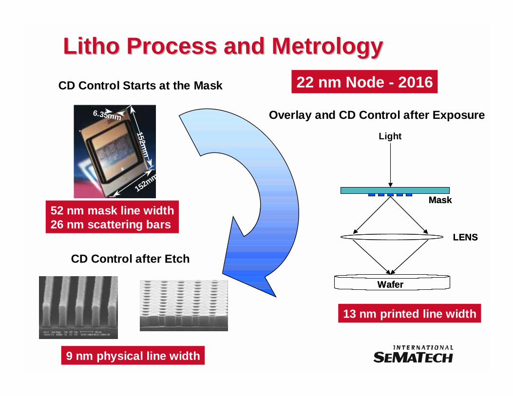
Litho Process and MetrologyLitho Process and MetrologyCD Control Starts at the Mask
152mm
152mm
6.35mm Overlay and CD Control after Exposure
CD Control after Etch
13 nm printed line width
9 nm physical line width
52 nm mask line width26 nm scattering bars
22 nm Node - 2016
Light
Mask
LENS
Wafer
Light
Mask
LENS
Wafer

Optical LithographyOptical LithographyFeature Size vs Wavelength
0
100
200
300
400
500
1994 1998 2002 2006 2010 2014
Year
Nod
e (n
m)
248 nm
193 nm
157 nm
EUV
CD < λλλλ/2

Litho MetrologyLitho MetrologyEUV
EUV193 and 157 nm
193 nm
157 nm
Technology Node 130 nm 90nm 65 nm 45 nm 32 nm 22 nm DriverLithography Metrology
Printed Gate CD Control (nm) 5.3 3 2 1.5 1.1 0.7 MPU
Wafer CD 3σ Precision P/T=0.2 1.1 0.6 0.4 0.3 0.2 0.1 MPU
Line Edge Roughness (nm) 4.5 2.7 1.8 1.3 0.9 0.65 MPU
Precision for LER 0.9 0.54 0.36 0.26 0.18 0.13

Physics of Resolution• Resolution W = k λλλλ/NA
• To print small features use smaller the wavelengths
• Use tricks to Print features sizes close to the wavelength
λλλλ is the wavelength of the lightNA is the numerical aperture NA = ηηηηsinθθθθ ηηηη is index of refractionK is a constant that depends on the process
See Principles of Lithography, H. Levinson, p 19

Physics of Depth of Focus• DoF = k2 λλλλ/ (NA)2 λλλλ>> feature size
• To print small features use smaller the wavelengths
• Use tricks to Print features sizes close to the wavelength
λλλλ is the wavelength of the lightNA is the numerical aperture NA = ηηηηsinθθθθ ηηηη is index of refractionK is a constant that depends on the process
See The Rayleigh Depth of Focus, C. Mack, Microlithography World: Feb 2004

Tricks to extend Optical LithographyTricks to extend Optical LithographyMask features that do not printMask features that do not print
Optical Proximity Corrections Phase Shift Masks
Light
Mask
LENS
Wafer
Light
Mask
LENS
Wafer
TOP View
SIDE View
ContactContactW/ OPC
Isolated Line w/Scattering Bars
Alternating Phase Shift
Rim Phase Shift
Many other types

Immersion LENS• Change NA by changing refractive index
from air ηηηη = 1 to water ηηηη = 1.46
• Extends 193 nm Litho to smaller feature sizes W(immersion)/W(dry) = 1/1.46 ~ 0.7
• DoF(immersion)/DoF (dry) at 193 nm
See The Rayleigh Depth of Focus, C. Mack, Microlithography World: Feb 2004

Low Energy SEM for CD MeasurementsLow Energy SEM for CD Measurements
Thanks to David Joy
FE source
Lens
Scanning coils
Sample Stage
wafer
Secondary ElectronDetector
Top DownImage

10 nm
20 nm
TBW = ζζζζ
CD
Gabor’s limit5 nm
TBW = ζζζζ
CD
Limits of SEM for CD MeasurementsLimits of SEM for CD Measurements
Thanks to David Joy
DoF = (resolution)/(convergence
angle)
Loss of Depth of Field

50 nm
50 nm
?
Challenges: Round Top Resist & LERChallenges: Round Top Resist & LER
Line Edge RoughnessRequires Better Dimensional Precision
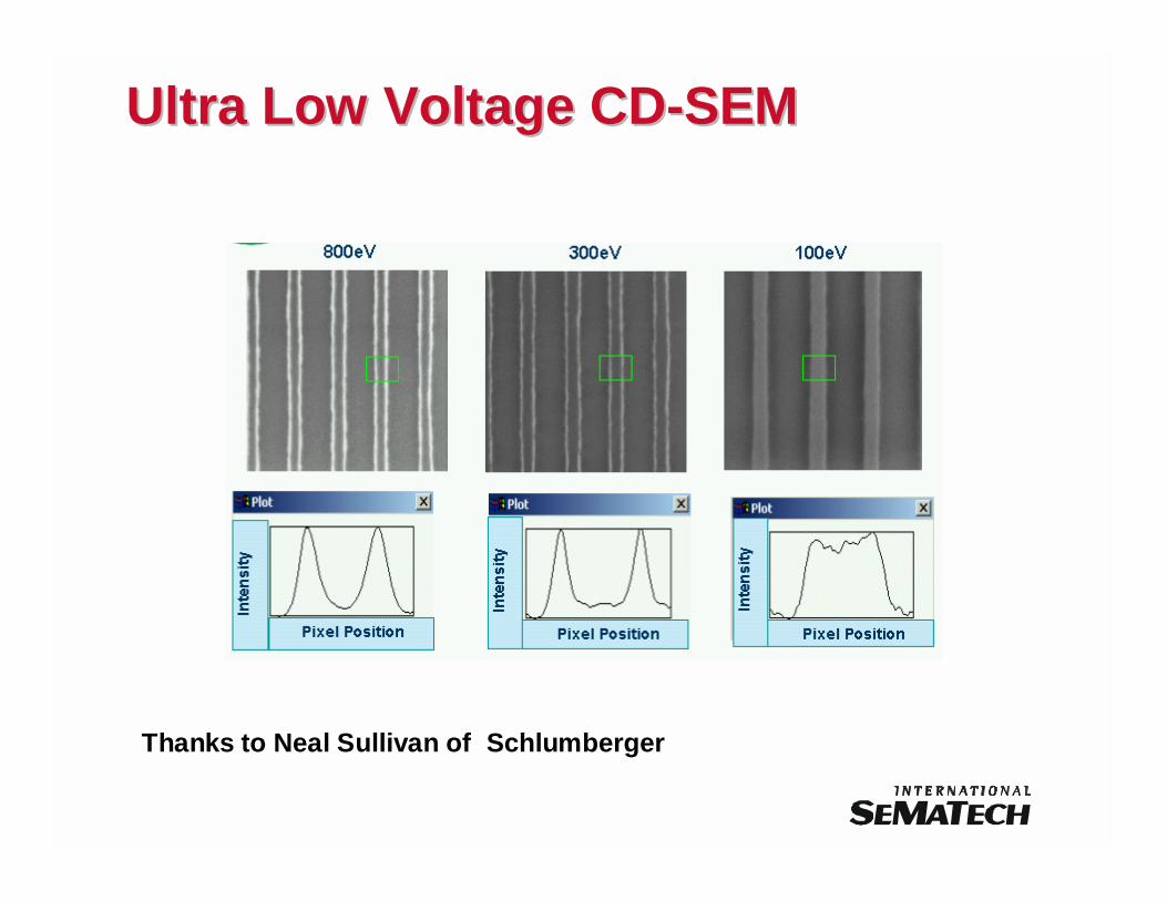
Ultra Low Voltage CDUltra Low Voltage CD--SEMSEM
Thanks to Neal Sullivan of Schlumberger

Lithography CD MetrologyLithography CD MetrologyImprove CDImprove CD--SEM thru 65 nm nodeSEM thru 65 nm node
Comparison of conventional SE (left) and Low Loss (right) images of copper
interconnects. Note the greatly enhanced surface detail and lack of edge brightness in
the Low Loss image.
Micrograph courtesy of O C Wells
Figures from David Joy
High Voltage CD-SEM
100 – 200 keVe-
Low loss detector

3D CD Metrology3D CD Metrology SEM SEM –– Scatterometry Scatterometry –– CDCD--AFMAFM
Commercially available R&DSoftware comparison of top
down line scan of edge to golden image
Tilt Beam SEM
Scatterometry
CD-AFM
Dual Beam FIB(destructive)
-480 -400 -320 -240 -160 -80 0 80 1600
100
200
300
400
500
600
5
-480 -400 -320 -240 -160 -80 0 80 1600
100
200
300
400
500
600
5
Software to convert top down image to
3D image

PolarizationSensitiveDetector
Incident PolarizedWhite Light
0th order
Multi-wavelengthLight Source
Mirror
ΘΘΘΘ in = ΘΘΘΘ out
Scatterometry Scatterometry for CD Measurementsfor CD Measurements
-480 -400 -320 -240 -160 -80 0 80 1600
100
200
300
400
500
600
5
-480 -400 -320 -240 -160 -80 0 80 1600
100
200
300
400
500
600
5
Real Time Calculation of line width & shapeEliminates Libraries

CDCD--AFM Limited by Probe Tip AFM Limited by Probe Tip
Carbon Nanotube Probe tips

Average Average vs vs IndividualIndividual
• CD-SEM measures one line at a time
• Scatterometry gives an average over many lines
• Reports indicate a large number (80 different lines) CD-SEM measurements in test area required to match scatterometry average
• Lose individual line information

AGENDAAGENDA
• The ITRS Challenge
• Litho Processes and Metrology
• FEP Processes and Metrology
• Interconnect Processes and Metrology
• Materials Characterization

Front End Processes & MetrologyFront End Processes & MetrologyShallow Trench Isolation Pattern &
Implant Wells
Pattern & Gate Dielectric
Pattern Poly/metalImplant LDD
Pattern & Implant S/D
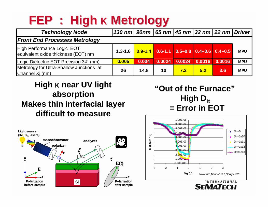
FEP : High FEP : High κκκκκκκκ MetrologyMetrology
0.00E+001.00E-072.00E-073.00E-074.00E-075.00E-076.00E-077.00E-078.00E-079.00E-071.00E-06
-3 -2 -1 0 1 2 3
Vg (V)
C (F
/cm
^2)
Dit=0
Dit=1e10
Dit=1e11
Dit=1e12
Dit=1e13
tox=3nm,Nsub=1e17,Npoly=1e20
“Out of the Furnace” High Dit
= Error in EOT
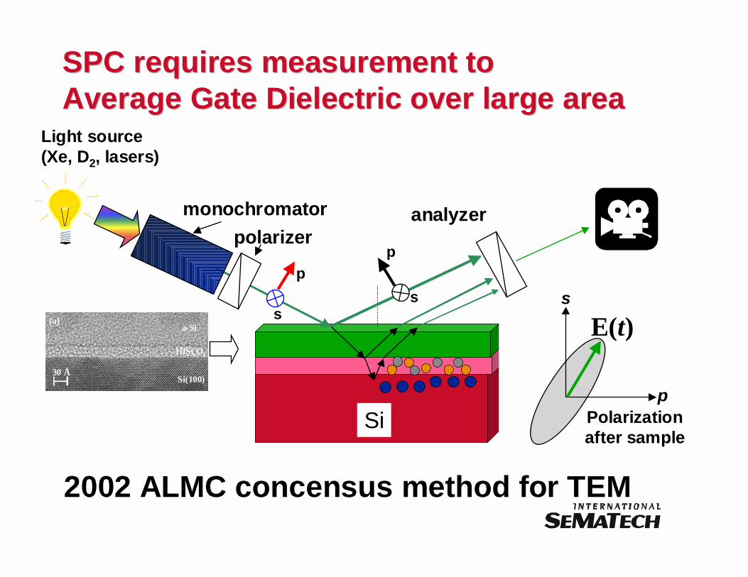
polarizeranalyzermonochromator
Es
p
Polarizationbefore sample
s
p
E(t)
Polarizationafter sample
p
s
p
s
Si
polarizeranalyzermonochromator
Es
p
Polarizationbefore sample
s
p
E(t)
Polarizationafter sample
p
s
p
s
Si
Light source:(Xe, D2, lasers)
High κκκκ near UV light absorption
Makes thin interfacial layer difficult to measure
Technology Node 130 nm 90nm 65 nm 45 nm 32 nm 22 nm DriverFront End Processes MetrologyHigh Performance Logic EOTequivalent oxide thickness (EOT) nm 1.3-1.6 0.9-1.4 0.6-1.1 0.5–0.8 0.4–0.6 0.4–0.5 MPU
Logic Dielectric EOT Precision 3σ (nm) 0.005 0.004 0.0024 0.0024 0.0016 0.0016 MPUMetrology for Ultra-Shallow Junctions at Channel Xj (nm) 26 14.8 10 7.2 5.2 3.6 MPU

Optical/XOptical/X--ray ray vs vs Electrical MeasurementElectrical MeasurementC-V Structures receive Further ProcessingOptical thickness vs electrical EOTCapacitance of a very thin interface can have big effect
See also : C Richter in Char & Met for ULSI 2000
poly-Si
Si-substrate
Traditional Electrical
C interface
Cox.
Vpoly depletion
Vgate
tint.
tox.
Optical Physical(Process Monitoring) (Performance/Reliability)
dielectric
QM charge
toptical = t int + t high κκκκ
EOT = t int + (3.9/κκκκ)thigh κκκκ
polarizeranalyzermonochromator
p
s
E(t)
Polarizationafter sample
p
s
p
s
Si
Light source(Xe, D2, lasers)
SPC requires measurement to SPC requires measurement to Average Gate Dielectric over large areaAverage Gate Dielectric over large area
Si(100)
a-Si
HfSixOy
(a)
30 ÅSi(100)
a-Si
HfSixOy
(a)
30 Å
2002 ALMC concensus method for TEM

Optical Constants
Photon Energy (eV)0.0 1.0 2.0 3.0 4.0 5.0 6.0 7.0
Rea
l(Die
lect
ric C
onst
ant),
ε 1
Imag(D
ielectric Constant),
ε2
2.0
3.0
4.0
5.0
6.0
7.0
8.0
9.0
0.0
0.5
1.0
1.5
2.0
2.5
High K
SiO2
New Optical Models for higher New Optical Models for higher κκκκκκκκ
In-Line Metrology Suppliers continue to use older damped oscillator models

Simplified XSimplified X--ray Path for Xray Path for X--ray reflectometerray reflectometer
sampledetector
X-ray source
diffuse scatter
specularly reflected
beam
slits
slits
θθθθd
2 d sinθλλλλPhase shift =
Thanks to Rich Matyi
0090814-07 40Å HfO2 850°C/20s
Angle (arcseconds)0 3600 7200 10800 14400
Inte
nsity
(cou
nts
s-1)
10-1
100
101
102
103
104
105
106
experimental datasimulated profile
4 nm HfO2
Models can include interface layer

Extra reflection from SOI Wafers Impacts Optical Extra reflection from SOI Wafers Impacts Optical Measurements and Light ScatteringMeasurements and Light Scattering
SOI WaferSOI WaferSi WaferSi Wafer
Gate Dielectric Gate Dielectric on Si Waferon Si Wafer
Gate Dielectric Gate Dielectric on SOI Waferon SOI Wafer
SOI WaferSOI WaferSOI WaferSOI WaferSi WaferSi WaferSi WaferSi Wafer
Gate Dielectric Gate Dielectric on Si Waferon Si Wafer
Gate Dielectric Gate Dielectric on Si Waferon Si Wafer
Gate Dielectric Gate Dielectric on SOI Waferon SOI Wafer
Gate Dielectric Gate Dielectric on SOI Waferon SOI Wafer
Quantum confinement for sub 20 nm siliconNeed SOI Optical Constants

AGENDAAGENDA
• The ITRS Challenge
• Litho Processes and Metrology
• FEP Processes and Metrology
• Interconnect Processes and Metrology
• Materials Characterization

Interconnect Processes & MetrologyInterconnect Processes & Metrology
Low k / barrieretch stop / low k
Pattern Low κκκκ
Deposit barrier and copper
Chemical Mechanical Polishing
Control Line width/depth and shape
Control barrier/copper & voiding
Control Flatness

Gaps in Interconnect MetrologyGaps in Interconnect Metrology
• VOID Detection in Copper lines
• Killer Pore Detection in Low κκκκ
• Barrier / Seed Cu on sidewalls
• Control of each new Low κκκκ
Technology Node 130 nm 90nm 65 nm 45 nm 32 nm 22 nmInterconnect MetrologyBarrier layer thick (nm) process range (±3σ ) Precision 1σ (nm)
1320%0.04
1020%0.03
720%0.02
520%0.016
420%0.013
Void Size for 1% Voiding in Cu Lines 87 52 37 26 18 12Detection of Killer Pores at (nm) size 6.5 4.5 3.25 2.25 1.6 1.1

Capacitance Test
Resistance Test
RR--C test structures of new low C test structures of new low κκκκκκκκPrior to manufacturePrior to manufacture

10 -5
10 -4
10 -3
10 -2
10 -1
10 0
Ref
lect
ivity
2.01.51.00.50.0
Scattering Angle 2 θ /Deg.
1101807-08 Raw Data Fitted Data
0.2 µm
Porous Low-k391.1 nm
SiNC 15 nm (density 1.89g/cm3)SiNC 3 nm (density 1.70g/cm3)
SiO2 (density 2.14 g/cm3)550 nm
SiNC 15 nm (density 1.89g/cm3)SiNC 3 nm (density 1.70g/cm3)
SiNC 15 nm (density 1.89g/cm3)SiNC 3 nm (density 1.70g/cm3)
18 nm
6 periods
Si substrate
XRR for low XRR for low κκκκκκκκ process controlprocess control
p(r
)
0 10 20 30 40 50 60 700.000
0.010
0.020
0.030
0.040
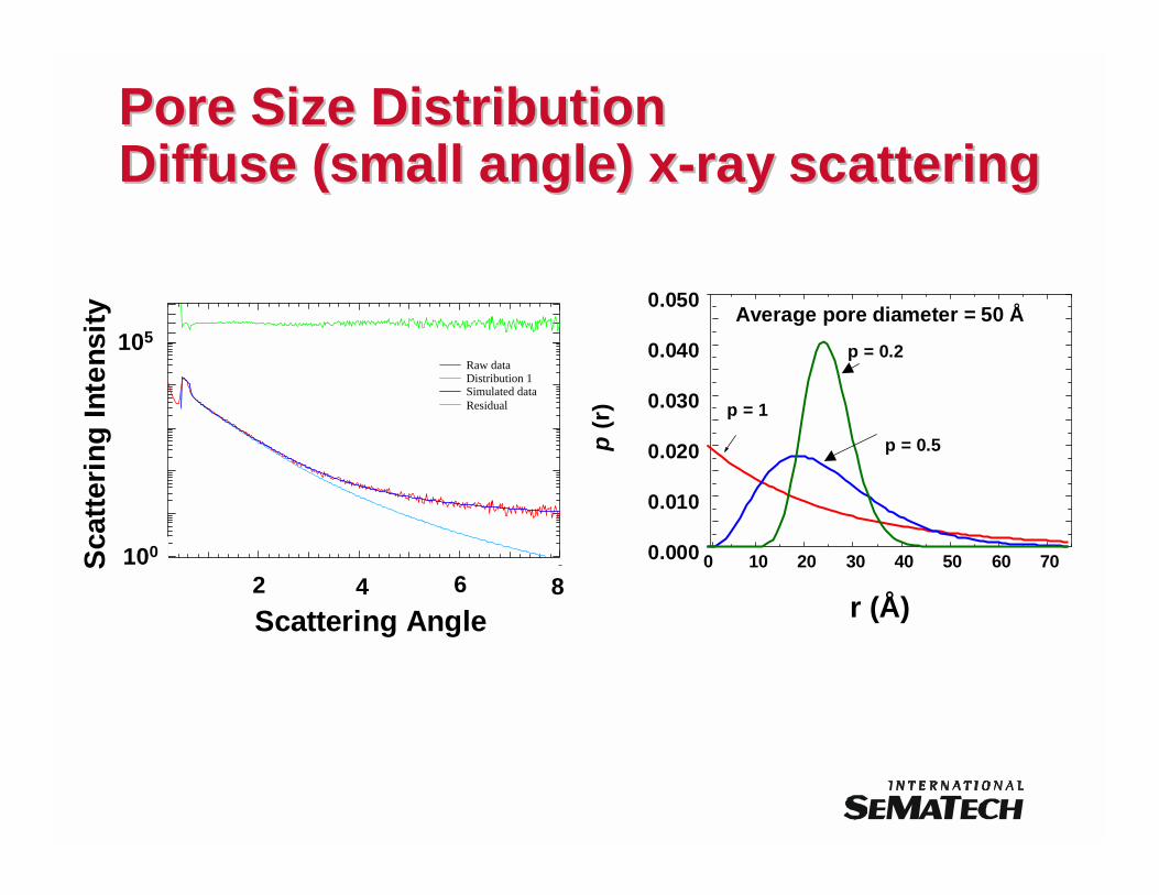
0.050Average pore diameter = 50 Å
p = 0.2
p = 0.5
p = 1
r (Å)
100
101
102
103
104
105
Scat
terin
g In
tens
ity /C
PS
8642
Scattering Angle 2θ /Deg.
Raw data Distribution 1 Simulated data Residual
Scattering Angle2 4 6 8
Scat
teri
ng In
tens
ity
105
100
Pore Size DistributionPore Size DistributionDiffuse (small angle) xDiffuse (small angle) x--ray scatteringray scattering

AGENDAAGENDA
• The ITRS Challenge
• Litho Processes and Metrology
• FEP Processes and Metrology
• Interconnect Processes and Metrology
• Materials Characterization

Method Dependent Observation of Method Dependent Observation of Film PropertiesFilm Properties
Silicon Wafer on a Wafer Chuck
Local informationHRTEM of SiO2 Thickness

TEM Imaging of the InterfaceTEM Imaging of the Interface
Distance
Mea
sure
d Pr
ofile
Incidentbeam
Distance
Mea
sure
d Pr
ofile
Incidentbeam

a b
Smooth Interface
Rough Interface SiO2
Silicon
Thanks to Dave Muller
TEM of thin gate dielectricTEM of thin gate dielectricSimulation and Experimental Data Simulation and Experimental Data show ADFshow ADF--STEM and HRSTEM and HR--TEM give TEM give same thicknesssame thickness
Consensus method uses 50 nm thick sample & ADF-STEM

xy
z
Vex
Vaccel
Vpulseb
Local Electrode Atom ProbeLocal Electrode Atom Probe
Atom Distribution
: < 100% detection

Metrology & New StructuresMetrology & New Structures
DEVICE RESONANT TUNNELING DIODE – FET
SINGLE ELECTRON
TRANSISTOR
RAPID SINGLE QUANTUM FLUX
LOGIC
QUANTUM CELLULAR AUTOMATA
NANOTUBE DEVICES MOLECULAR DEVICES
TYPES 3-terminal 3-terminal
Josephson Junction
+inductance loop
-Electronic QCA -Magnetic QCA FET 2-terminal and
3-terminal
STORAGE MECHANISM
BASELINE 2002 TECHNOLOGIES MAGNETIC RAM PHASE CHANGE
MEMORY NANO FLOATING GATE MEMORY
SINGLE/FEW ELECTRON MEMORIES
MOLECULAR MEMORIES
DEVICE TYPES DRAM NOR FLASH PSEUDO-
SPIN- VALVE
MAGNETIC TUNNEL
JUNCTION OUM
-ENGINEERED TUNNEL BARRIER
-NANOCRYSTAL SET
-BISTABLE SWITCH
-MOLECULAR NEMS
-SPIN BASED MOLECULAR
DEVICES
WORD BIT
W
R n + n + memor y nod e Engineered barrier
Si Gate
Logic
Memory

Metrology & Molecular ElectronicsMetrology & Molecular Electronics
James Heath, Fraser Stoddart, and Anthony Pease

A
B
C
Metrology & Molecular ElectronicsMetrology & Molecular Electronics
Paul Weiss’s Group – STM of Conductance Switching
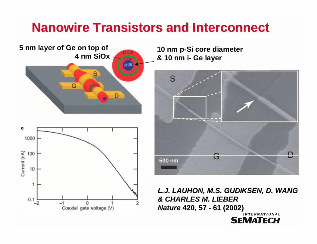
Nanowire Nanowire Transistors and InterconnectTransistors and Interconnect
L.J.L.J. LAUHON, M.S.LAUHON, M.S. GUDIKSEN, D.GUDIKSEN, D. WANG WANG & CHARLES& CHARLES M.M. LIEBERLIEBERNatureNature 420, 57 420, 57 -- 61 (2002)61 (2002)
500 nm
10 nm p-Si core diameter & 10 nm i- Ge layer
5 nm layer of Ge on top of 4 nm SiOx

ConclusionsConclusions
• There are many opportunities for the Physics Community in the area of future IC technology
• Nanoelectronics is here!
• Metrology is a Key Enabler!

Use of HRTEM for CalibrationUse of HRTEM for CalibrationHigh Resolution TEM (Phase Contrast)High Resolution TEM (Phase Contrast)has a ~ 10% error for Thickness Determination Due to Cshas a ~ 10% error for Thickness Determination Due to Cs
HRTEM Image Simulations for Gate Oxide Metrology
S. Taylor, J. Mardinly, M.A. O’Keefe, and R. GronskyCharacterization and Metrology for ULSI Technology 2000
Specimen Thickness
A
Specimen Tilt (mrad) Defocus Cs
(mm)
Oxide Model
Thickness
Oxide Measured Thickness
% Error
154 0 -425 0.5 10.56 9.84 -6.8154 0 -156 0.5 10.56 11.4 8154 0 -20 0.5 10.56 10.44 -1.1154 12.6 -425 0.5 10.56 9.12 -13.6154 25 -425 0.5 10.56 10.68 1.1154 0 -425 0.5 10.56 8.88 -15.9