Physical Electronics Slides of Chapter 5 (All...
39
PHYSICAL ELECTRONICS(ECE3540) Brook Abegaz, Tennessee Technological University, Fall 2013 Wednesday, October 02, 2013 Tennessee Technological University 1 CHAPTER 5 – CARRIER TRANSPORT PHENOMENA
Transcript of Physical Electronics Slides of Chapter 5 (All...

PHYSICAL ELECTRONICS(ECE3540)
Brook Abegaz, Tennessee Technological University, Fall 2013
Wednesday, October 02, 2013Tennessee Technological University 1
CHAPTER 5 – CARRIER TRANSPORT PHENOMENA

Chapter 5 – Carrier Transport Phenomena
Chapter 4: we considered the semiconductorin equilibrium and determined electron and holeconcentrations in the conduction and valencebands, respectively.
The net flow of the electrons and holes in asemiconductor will generate currents. The processby which these charged particles move is calledtransport.
Chapter 5: we will consider the two basictransport mechanisms in a semiconductor crystal:drift the movement of charge due to electric fields,and diffusion the flow of charge due to densitygradients.
Wednesday, October 02, 2013Tennessee Technological University 2

An electric field applied to a semiconductor willproduce a force on electrons and holes so that theywill experience a net acceleration and net movement,provided there are available energy states in theconduction and valence hands.
This net movement of charge due to an electric fieldis called drift. The net drift of charge gives rise to adrift current.
Drift Current Density: for a positive volumecharge density p moving at an average drift velocityvd, the drift current density is given by:
where J is in units of C/cm2-s or amps/cm2.
Wednesday, October 02, 2013Tennessee Technological University 3
Carrier Drift
ddrf vJ

If the volume charge density is due to positively charged holes,then :
where Jp|drf is the drift current density due to holes and vd|p is theaverage drift velocity of the holes.
The equation of motion of a positively charged hole in thepresence of an electric field is:
where e is the magnitude of the electronic charge, a is theacceleration, E is the electric field, and mp
* is the effective mass ofthe hole.
If the electric field is constant, then we expect the velocity toincrease linearly with time. However, charged particles in asemiconductor are involved in collisions with ionized impurityatoms and with thermally vibrating lattice atoms. These collisions,or scattering events, alter the velocity characteristics of the particle.
Wednesday, October 02, 2013Tennessee Technological University 4
Carrier Drift
pddrfp vepJ || )(
eEamF p *

As the hole accelerates in a crystal due to the electric field, the velocity increases. When thecharged particle collides with an atom in the crystal, the particle loses most or all of its energy.
The particle will again begin to accelerate and gain energy until it is again involved in ascattering process. Throughout this process, the particle will gain an average drift velocitywhich, for low electric fields, is directly proportional to the electric field. We may then write
where p, is the proportionality factor and is called the hole mobility. The mobility of asemiconductor describes how well a particle will move due to an electric field. The unit ofmobility is expressed in terms of cm2/V-s.
By combining the above equations, we may write the drift current density due to holes as
The drift current due to holes is in the same direction as the applied electric field. The same discussion of drift applies to electrons.
Where Jn|drf is the drift current density due to electrons and vdn is the average drift velocity of electrons. The net charge density of electrons is negative.
Wednesday, October 02, 2013Tennessee Technological University 5
Carrier Drift
Ev pdp
pEevepJ pdpdrfp )(|
dndndrfn venvepJ )()(|

The average drift velocity of an electron is also proportional tothe electric field for small fields. However, since the electron isnegatively charged, the net motion of the electron is opposite tothe electric field direction. Therefore,
where μn is the electron mobility and is a positive quantity.
The conventional drift current due to electrons is also in the samedirection as the applied electric field even though the electronmovement is in the opposite direction.
Electron and hole mobilities are functions of temperature anddoping concentrations.
Since both electrons and holes contribute to the drift current, thetotal drift current is the sum of the individual electron and holedrift current densities, therefore:
Wednesday, October 02, 2013Tennessee Technological University 6
Carrier Drift
Ev ndn
nEeEenJ nndrfn ))((|
EpneJ pndrf )(

Exercise1. Consider a Gallium Arsenide sample which is
at T = 300K and with doping concentrationsof Na =10cm-3 and Nd = 1016 cm-3. Assume acomplete ionization and assume electron andhole mobilities given in Table 5.1. Calculate thedrift current density if the applied electric fieldis E = 10V/cm2.
Wednesday, October 02, 2013Tennessee Technological University 7

Solution1. Using the formula:
The minority carrier hole concentration is:
The drift current density for this extrinsic n-type semiconductor is:
Wednesday, October 02, 2013Tennessee Technological University 8
31622 10)2
(2
)(
cmnNNNNn iadad
3416
262
10*24.3)10*1()10*8.1( cm
nnp i
2136)()(cm
AENeEpneJ dnpndrf
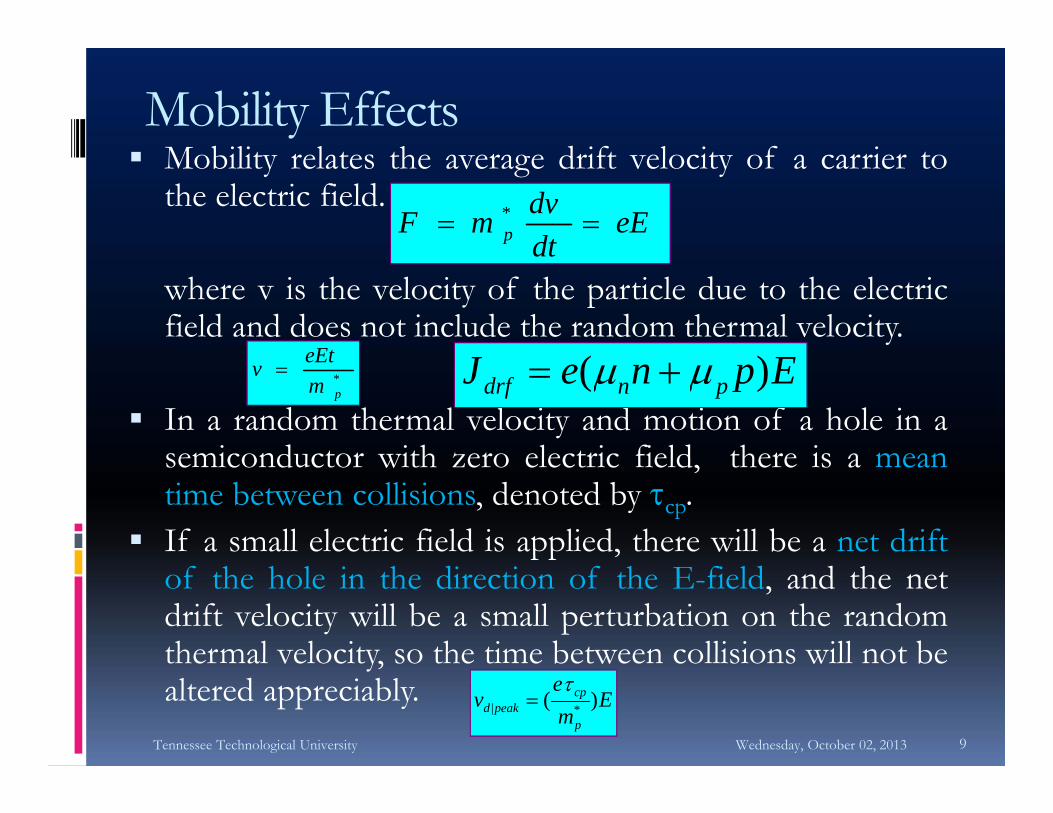
Mobility relates the average drift velocity of a carrier tothe electric field.
where v is the velocity of the particle due to the electricfield and does not include the random thermal velocity.
In a random thermal velocity and motion of a hole in asemiconductor with zero electric field, there is a meantime between collisions, denoted by cp.
If a small electric field is applied, there will be a net driftof the hole in the direction of the E-field, and the netdrift velocity will be a small perturbation on the randomthermal velocity, so the time between collisions will not bealtered appreciably.
Wednesday, October 02, 2013Tennessee Technological University 9
Mobility Effects
*pm
eEtv EpneJ pndrf )(
eEdtdvmF p *
Eme
vp
cppeakd )( *|

The average drift velocity is one half the peak value:
Statistically, the hole mobility and the electronmobility are given as:
where n is the mean time between collisions for anelectron.
There are two collision or scattering mechanismsthat dominate in a semiconductor and affect thecarrier mobility: phonon or lattice scattering andionized impurity scattering.
Wednesday, October 02, 2013Tennessee Technological University 10
Mobility Effects
Eme
vp
cpd )(
21
*
*p
cpdpp m
eEv
*n
cnn m
e

The atoms in a semiconductor crystal have a certainamount of thermal energy at temperatures above absolutezero that causes the atoms to randomly vibrate about theirlattice position within the crystal. The lattice vibrationscause a disruption in perfect periodic potential function.
A perfect periodic potential in a solid allows electrons tomove unimpeded, or with no scattering, through the crystal.
Thermal vibrations however cause a disruption of thepotential function, resulting in an interaction between theelectrons or holes and the vibrating lattice atoms. Thislattice scattering is also referred to as phonon scattering.
Since lattice scattering is related to the thermal motion ofatoms, the rate at which the scattering occurs is a functionof temperature. If we denote μL as the mobility observed ifonly lattice scattering existed, then the scattering theorystates the relation to first order:
Wednesday, October 02, 2013Tennessee Technological University 11
Phonon or Lattice Scattering
23
TL

Impurity atoms are added to the semiconductor tocontrol or alter its characteristics. These impuritiesare ionized at room temperature so that a Coulombinteraction exists between the electrons or holes andthe ionized impurities. This coulomb interactionproduces scattering or collisions and also alters thevelocity characteristics of the charge carrier. If wedenote μI as the mobility that would be observed ifonly ionized impurity scattering existed, then:
where NI = Nd+ + Na
- is the total ionized impurityconcentration in the semiconductor.
Wednesday, October 02, 2013Tennessee Technological University 12
Ionized Impurity Scattering
II N
T 23

If temperature increases, the random thermalvelocity of a carrier increases, reducing the time thecarrier spends in the vicinity of the ionized impuritycenter.
The less time spent in the vicinity of a coulombforce, the smaller the scattering effect and the largerthe expected value of μI.
If the number of ionized impurity centersincreases, then the probability of a carrierencountering an ionized impurity center increases,implying a smaller value of μI.
Wednesday, October 02, 2013Tennessee Technological University 13
Ionized Impurity Scattering
II N
T 23

If these two scattering processes are independent,then the total probability of a scattering eventoccurring in the differential time dt is the sum ofthe individual events, or
where μI is the mobility due to the ionized impurityscattering process and μL is the mobility due to thelattice scattering process. The parameter μ is the netmobility.
Wednesday, October 02, 2013Tennessee Technological University 14
Lattice + Ionized Impurity Scattering
LI
dtdtdt
LI 111

The drift current density is given as:
where is the conductivity of the semiconductor material. The reciprocal of conductivity is resistivity.
Wednesday, October 02, 2013Tennessee Technological University 15
Conductivity
EEpneJ pndrf )(
)(11
pne pn

Exercise Consider compensated n-type silicon at T = 300
K, with a conductivity of =16(Ohm-cm)-1 and an acceptor doping concentration of 1017 cm-3. Using the donor concentration Nd = 2*1017cm-3
find the electron mobility.
Wednesday, October 02, 2013Tennessee Technological University 16

SolutionUsing:
We can solve for n = 510cm2/Vs.
Wednesday, October 02, 2013Tennessee Technological University 17
)( pne pn

Diffusion: is the process by which particles flowfrom a region of high concentration toward aregion of low concentration (density gradient).
If the distance l is the mean-free path of anelectron or the average distance an electron travelsbetween collisions (l = vthcn), then, electronsmoving to the right at x = -l and electrons movingto the left at x = +l will cross the x = 0 plane.
One half of the electrons at x = -l will be travellingto the right at any instant of time and one half ofthe electrons at x = +l will be traveling to the left atany given time. The net rate of electron flow, Fn is:
Wednesday, October 02, 2013Tennessee Technological University 18
Carrier Diffusion
)](21)([
21)(
21)(
21 lnlnvvlnvlnF thththn
X=0X=-l X=+l

Expanding the electron concentration in a Taylorseries about x = 0, keeping the first two terms, then:
which becomes:
Each electron has a charge of (-e) therefore:
Therefore, the electron diffusion current isproportional to the spatial derivative or the densitygradient of the electron concentration.
Wednesday, October 02, 2013Tennessee Technological University 19
Carrier Diffusion
]})0([])0({[21
dxdnln
dxdnlnvF thn
dxdnlvF thn
dxdnleveFJ thn

Since electrons have a negative charge, theconventional current direction is in the positive xdirection. The electron diffusion current density forthe one-dimensional case is:
where Dn is called the electron diffusion coefficient,has units of cm2/s, and is a positive quantity. If theelectron density gradient becomes negative, theelectron diffusion current density will be in thenegative x direction.
Wednesday, October 02, 2013Tennessee Technological University 20
Carrier Diffusion
dxdneDJ ndifnx |

Since holes are positively charged particles, theconventional diffusion current density is in thenegative x direction. The hole diffusion currentdensity is proportional to the hole density gradientand to the electronic charge, as:
where Dp is the hole diffusion coefficient with unitsof cm2/s.
Wednesday, October 02, 2013Tennessee Technological University 21
Carrier Diffusion
dxdpeDJ pdifpx |

Exercise Assume that in an n-type Gallium Arsenide
semiconductor at T = 300 K, the electronconcentration varies linearly from 1 x 10¹⁸ to7 x1017cm-3 over a distance of 0.10 cm. Calculatethe diffusion current density if the electrondiffusion coefficient is Dn = 225 cm2/s.
Wednesday, October 02, 2013Tennessee Technological University 22
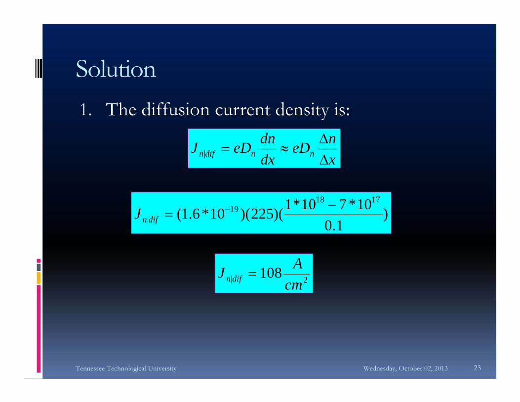
Solution1. The diffusion current density is:
Wednesday, October 02, 2013Tennessee Technological University 23
xneD
dxdneDJ nndifn
|
)1.0
10*710*1)(225)(10*6.1(1718
19|
difnJ
2| 108cm
AJ difn
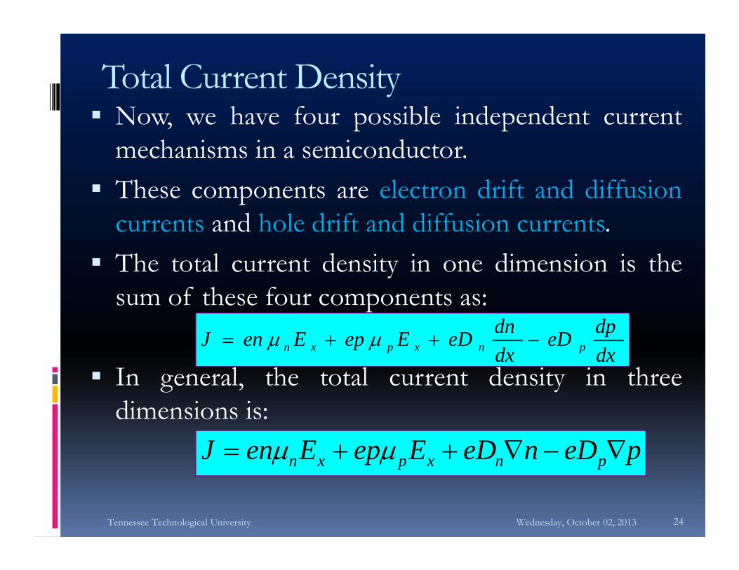
Now, we have four possible independent currentmechanisms in a semiconductor.
These components are electron drift and diffusioncurrents and hole drift and diffusion currents.
The total current density in one dimension is thesum of these four components as:
In general, the total current density in threedimensions is:
Wednesday, October 02, 2013Tennessee Technological University 24
Total Current Density
dxdpeD
dxdneDEepEenJ pnxpxn
peDneDEepEenJ pnxpxn

The diffusion coefficient and mobility are notindependent parameters. They are related using theEinstein Relation.
Consider a non-uniformly doped semiconductorand assume there are no electrical connections sothat the semiconductor is in thermal equilibrium,then the electron and hole currents must be zero.
Assuming quasi neutrality, n ≈ Nd , and substitutingfor electric field, we find the Einstein Relation:
Wednesday, October 02, 2013Tennessee Technological University 25
The Einstein Relation
dxdneDEenJ nxnn 0
ekTDD
p
p
n
n

Exercise Assume that the mobility of a particular carrier
is 1000 cm2/V-s at T = 300 K. Determine thediffusion coefficient for the given the carriermobility.
Wednesday, October 02, 2013Tennessee Technological University 26

Solution1. Using the Einstein relation,
Note: The diffusion coefficient is approximately 40 times smaller than the mobility of the carrier at room temperature.
Wednesday, October 02, 2013Tennessee Technological University 27
)1000)(0259.0()( e
kTD
scmD
2
9.25

At low electric fields, where there is a linearvariation of velocity with electric field, the slope ofthe drift velocity versus electric field curve is themobility ().
The behavior of the drift velocity of carriers at highelectric fields deviates substantially from the linearrelationship.
The drift velocity of electrons in Silicon, forexample, saturates at approximately 107cm/s at anelectric field of around 30kV/cm.
Therefore, at saturation, drift current density alsosaturates and becomes independent of applied field.
Wednesday, October 02, 2013Tennessee Technological University 28
Velocity Saturation

Wednesday, October 02, 2013Tennessee Technological University 29
Velocity Saturation

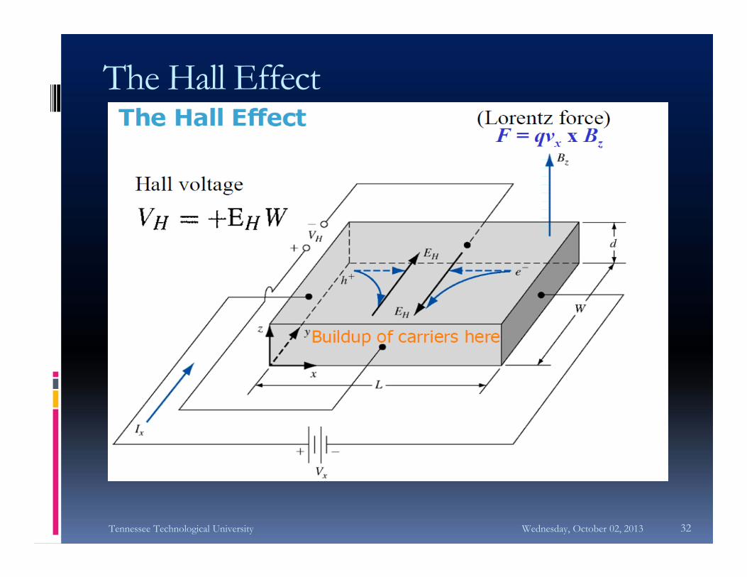
The Hall effect is a consequence of the forces thatare exerted on moving charges by electric andmagnetic fields.
The Hall effect is used to distinguish whether asemiconductor is an n-type or a p-type and tomeasure the majority carrier concentration andmajority carrier mobility.
The Hall effect device is used extensively inengineering applications: to experimentally measuresemiconductor parameters, as a magnetic probe andin other circuit applications.
Wednesday, October 02, 2013Tennessee Technological University 30
The Hall Effect

The force on a particle having a charge q andmoving in a magnetic field given by:
where the cross product is taken between velocity andmagnetic field so that the force vector is perpendicular toboth the velocity and magnetic field.
Wednesday, October 02, 2013Tennessee Technological University 31
The Hall Effect
)(vxBqF
Wednesday, October 02, 2013Tennessee Technological University 32
The Hall Effect

A semiconductor with a current Ix is placed in a magneticfield perpendicular to the current. In this case, themagnetic field is in the z direction.
Electrons and holes flowing in the semiconductor willexperience a force as indicated in the figure. The force onboth electrons and holes is in the (-y) direction.
In a p-type semiconductor (po > no), there will be abuildup of positive charge on the y = 0 surface of thesemiconductor and, in an n-type semiconductor (no > po),there will be a buildup of negative charge on the y = 0surface.
This net charge induces an electric field in the y-direction. In steady state, the magnetic field force will be exactly
balanced by the induced electric field force. This balancemay be written as:
Wednesday, October 02, 2013Tennessee Technological University 33
The Hall Effect
0]x[ BvEqF zxy BqvqE

The induced electric field in the y-direction is calledthe Hall Field. The Hall field produces a voltageacross the semiconductor which is called the HallVoltage:
where EH is positive in the +y direction and VH is positivewith shown polarity.
The polarity of the Hall Voltage is used todetermine if an extrinsic semiconductor is n-type orp-type. In a p-type semiconductor, the Hall Voltagewill be positive, and in an n-type semiconductor, theHall Voltage is negative.
Wednesday, October 02, 2013Tennessee Technological University 34
The Hall Effect
WEV HH

Substituting in
For a p-type semiconductor, the drift velocity ofholes is calculated as:
where e is the magnitude of electric charge. Combining the above two equations:
Solving for hole concentration,
Wednesday, October 02, 2013Tennessee Technological University 35
The Hall EffectWEV HH zxy BqvqE
zxH WBvV
))(( WdepI
epJv xx
dx
epdBIV zx
H
H
zx
edVBIp

Similarly for an n-type semiconductor, the Hall Voltage is:
The electron concentration is then: For a p-type semiconductor, the low-field majority carrier
mobility is:
The current density and electric field can be converted to current and voltage so that:
The hole mobility is then given by:
Similarly for an n-type semiconductor, the low-field electron mobility is determined from:
Wednesday, October 02, 2013Tennessee Technological University 36
The Hall Effect
WdepVLI
x
xp
WdenVLI
x
xn
nedBIV zx
H
H
zx
edVBIn
xpx EepJ
LVep
WdI xpx

Exercise Consider the geometry shown for measuring the
Hall Effect. Let L = 10-1 cm, W = 10-2 cm, d =10-3 cm. Also assume that Ix = 1.0 mA, Vx =12.5 V, Bz = 500 gauss = 5 x 10⁻² Tesla and VH= -6.25 mV. Determine the majority carrierconcentration and mobility, given the Hall effectparameters.
Wednesday, October 02, 2013Tennessee Technological University 37
H
zx
edVBIn
WdenVLI
x
xn
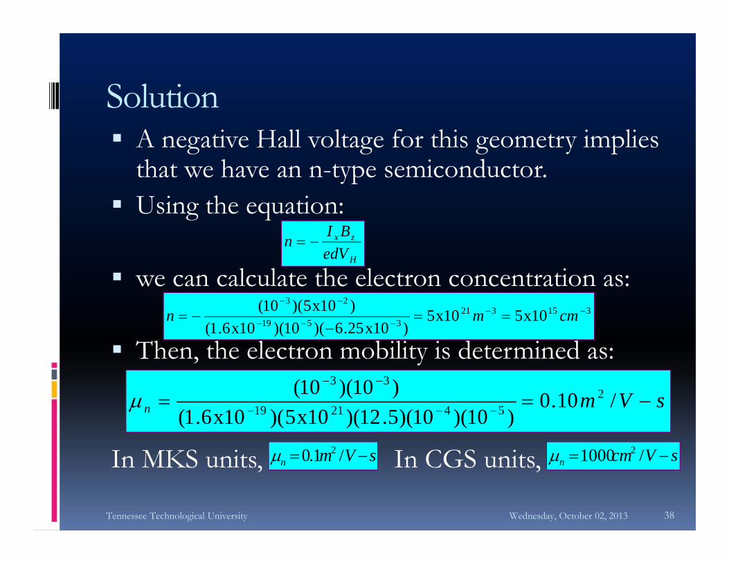
Solution A negative Hall voltage for this geometry implies
that we have an n-type semiconductor. Using the equation:
we can calculate the electron concentration as:
Then, the electron mobility is determined as:
In MKS units, In CGS units,
Wednesday, October 02, 2013Tennessee Technological University 38
sVmn
/10.0)10)(10)(5.12)(10x5)(10x6.1(
)10)(10( 2542119
33
sVcmn /1000 2sVmn /1.0 2
H
zx
edVBIn
3153213519
23
10x510x5)10x25.6)(10)(10x6.1(
)10x5)(10(
cmmn
Picture Credits Semiconductor Physics and Devices, Donald Neaman, 4th
Edition, McGraw Hill Publications. Carrier Transport Phenomena, Department of
Microelectronics, Delft University of Technology.http://ocw.tudelft.nl/courses/microelectronics/solid-state-physics/lectures/5-carrier-transport-phenomena/
The Semiconductor Module, COMSOL Multiphysicshttp://www.comsol.com/products/4.3b/
Wednesday, October 02, 2013Tennessee Technological University 39