PHYS 623 Field Programmable Gate Arrays Laboratory 1 · reprogrammable nature of FPGAs the logic...
12
PHYS 623 Field Programmable Gate Arrays Laboratory 1 Ian Wisher, University of Wisconsin Physics Department Last edits December 8, 2013 1 Primer In this lab we will explore one of the most exciting developments in digital hardware: the humble Field Programmable Gate Array or FPGA. The FPGA has asserted itself in the last decade as an integral part of both commercial and scientific electronics. The digital signal processing capabilities of FPGAs are partic- ularly fantastic which makes these devices invaluable for data acquisition systems. In addition, due to the reprogrammable nature of FPGAs the logic can be changed to repurpose the device or correct when bugs are found. This is great news for physicists who spend most of our career prototyping electronics that will never evolve past their prototype phase. 1.1 FPGA Basics FPGAs are made up of Logical Elements or discrete programmable blocks that can be programmed and connected together to form complex state machines and logic. Many FPGAs have specialized blocks for tasks that are used frequently and would take a large amount of resources if built from the Logical Elements. An example of these specialized blocks are adders, multipliers, Phase Lock Loops(for clock multiplication and division), and SRAM blocks. One important thing to note about FPGAs is that the programming is volatile in that once the FPGA loses power the programming is lost. Development boards like the DE0 we use in this lab have EEPROMs on the board to hold the programming information and load it on to the FPGA when the board is first powered on. 1.2 Choosing an FPGA When choosing an FPGA, like all electronics endeavors, its important to characterize your requirements and choose an FPGA that meets your requirements. Though you may consider a number of different characteristics and requirements (existence of specialized logic cores for example), there are a few properties to keep your eye on. • [Altera or Xilinx] - There are two main companies that manufacture/design FPGAs and both are very good. The only caveat that seems to be consistently true between the two manufactures is: Xilinx pushes to have most bells and whistles at the price of simplicity while Altera tends to prioritize ease 1
-
Upload
duongkhuong -
Category
Documents
-
view
215 -
download
0
Transcript of PHYS 623 Field Programmable Gate Arrays Laboratory 1 · reprogrammable nature of FPGAs the logic...
PHYS 623
Field Programmable Gate Arrays
Laboratory 1
Ian Wisher, University of Wisconsin Physics Department
Last edits
December 8, 2013
1 Primer
In this lab we will explore one of the most exciting developments in digital hardware: the humble FieldProgrammable Gate Array or FPGA. The FPGA has asserted itself in the last decade as an integral part ofboth commercial and scientific electronics. The digital signal processing capabilities of FPGAs are partic-ularly fantastic which makes these devices invaluable for data acquisition systems. In addition, due to thereprogrammable nature of FPGAs the logic can be changed to repurpose the device or correct when bugsare found. This is great news for physicists who spend most of our career prototyping electronics that willnever evolve past their prototype phase.
1.1 FPGA Basics
FPGAs are made up of Logical Elements or discrete programmable blocks that can be programmed andconnected together to form complex state machines and logic. Many FPGAs have specialized blocks fortasks that are used frequently and would take a large amount of resources if built from the Logical Elements.An example of these specialized blocks are adders, multipliers, Phase Lock Loops(for clock multiplicationand division), and SRAM blocks. One important thing to note about FPGAs is that the programming isvolatile in that once the FPGA loses power the programming is lost. Development boards like the DE0 weuse in this lab have EEPROMs on the board to hold the programming information and load it on to theFPGA when the board is first powered on.
1.2 Choosing an FPGA
When choosing an FPGA, like all electronics endeavors, its important to characterize your requirementsand choose an FPGA that meets your requirements. Though you may consider a number of differentcharacteristics and requirements (existence of specialized logic cores for example), there are a few propertiesto keep your eye on.
• [Altera or Xilinx] - There are two main companies that manufacture/design FPGAs and both arevery good. The only caveat that seems to be consistently true between the two manufactures is: Xilinxpushes to have most bells and whistles at the price of simplicity while Altera tends to prioritize ease
1

of use on the programmers. One should also download the software packages form both companies(Quartus for Altera and ISE for Xilinx) and determine which is more agreeable. One word of cautionthe licensing for the software seems to be archaic in many aspects: Xilinx ISE subscriptions are for useand not support so if your license expires you can no longer use the software. In this lab we use theDE0-nano board that has an Altera Cyclone IV and uses the Quartus software.
• [Logic Element Count] - This is the number of building blocks available for use in custom logic.This limits how complicated the logic you can implement inside the chip but for most cases there areusually more than enough of these.
• [Max Clock Frequency] - This is the max clock speed that the clock network is specified to run at.This is a good indication of the setup times for the flip flops in the FPGA which can give you an ideaof the frequency the chip could be sensitive to. It should be noted that there are different speed gradesof chips. Much like processors FPGAs are batched after testing into different grades depending on howthey perform in testing.
• [Price] - Pretty obvious why this is important.
• [Availability of Evaluation Boards] - For physicists/ prototyping engineers this is probably animportant factor since we will spend most of our time in development. The process of laying outa breakout board for an FPGA is not only strenuous and difficult but is often a multi-layer test ofattrition.
After considering the options above we’ve chosen to use the DE0 Cyclone IV development board from Terasic.However, this is by no means the dev board for all projects and you should feel free to try different boardsfor your future projects. This board was chosen because of its combination of support, low cost, and franklyspeaking : the author’s preferences for Altera.
Figure 1: Terasic System Builder with all the components enabled.
2
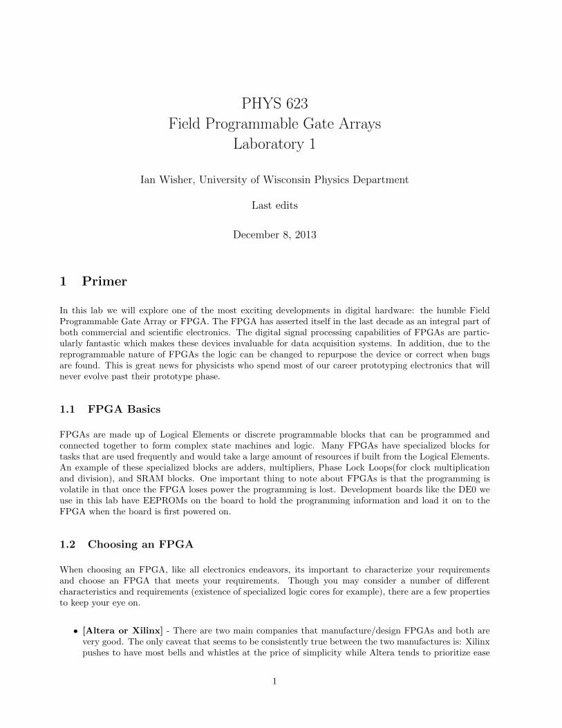
Figure 2: The layout of Quartus II showing the 4 main sections: project navigation, compilation summary,main work space, and the terminal
2 Getting Started
Now that we have our development board chosen we would then have to download and install the softwareneeded to compile code and eventually program the FPGA. Luckily for you the software has already beendownloaded and installed on the machines in the lab. In addition Terasic, the company that has suppliedthe development board, has provided tools that make starting a little easier.
2.1 Generating project files with Terasic Tools
The first step to programming an FPGA is to make a project that will hold all the different code youwould like to program on to the chip. Terasic has provided a program that will generate this project file aswell as assigning the pins correctly. It can be found in Users/Public/Lab Software/623/DE0-Nano-SystemBuilder.
Double click the System Builder executable and you should see something that looks like Figure 1. Make sure
3

that all the components are enabled and then make the project name something unique (like your name).Once you are satisfied click Generate and a folder located in the CodeGenerated folder will appear withthe project name that you chose. The standard location for this folder should be C:/Altera/DE0-Nano-SystemBuilder/CodeGenerated/DE0-Nano/, although almost any location will work.
Copy the folder with the name you chose into a safe location and open it. There should be a file withthe extension .qpf which stands for “Quartus project file” double click this and it will open your project inQuartus II (Altera’s Interactive Developer Environment). Note that there will be a file with a .qpf extensionand one with a .qsf extension. To see the extension you can select the file and right click to bring up theproperties window. Alternatively you can use the fact that the .qpf file is much smaller (about 1 kB).
2.2 Quartus Software Introduction
Quartus has a similar feel to many interactive development environments so if you have tried something likeeclipse or visual studio the organization will feel familiar. The main organization breaks down the code intoa discrete hierarchy from Project, Top Programing File (main function), and submodules.
The program should have opened with your top file being (the name of your project).v. This can beseen in the top left corner of the window or the project navigation panel. The Project navigation panel givesyou an overview of the code you are writing so you can see the hierarchy of your modules and submodules.The Panel just below that is the Tasks panel. Here you can compile your code and program the device oncecompilation is done. In addition, you can run simulations of your code to make sure that it will work beforeyou even load it onto the device. To the right is the workplace where files that are opened will be displayed.The bottom contains the terminal which will report compilation errors as well as other useful information.Now that you are familiar with the layout lets write our first FPGA program.
3 My First FPGA Code
To get started we first will create a schematic diagram. To do this first click on File→New→BlockDiagram/Schematic File. Once you click on Okay your diagram should appear on the workplace. We aregoing to add some inputs and outputs onto the diagram by right clicking on the diagram, as in Figure 3, andselecting insert→symbol. Bring the part you want to insert into the symbol window that opens by choosingfrom the library list on the left. Input/Output pins are located in: quartus/libraries/primitives/pin/ .When you have selected a part, close the symbol window. Mouse click in the schematic area to place a copyof the selected part. If you checked ”Repear-insert mode” you can place multiple copies with left clicks, thenpush the Esc key to stop. Otherwise, you can right-click to copy and paste additional copies where you wantthem. You will need one input pin and one output pin.
These pins now have to be identified with a particular pin on the FPGA package. We can make the schematicmore clear by assigning logical names showing what the pin is connected to instead using pin numbers. Foran example of this we can go to Assignments→ PinPlanner. A window like Figure 4 should show upwhich shows all the pin assignments that the Terasic system builder has already done for us. You can lookthrough the menus on the left and see which Altera pins are assigned to various peripheral devices andwhich are assigned to the header connector pins. You’ll need to refer to these exact names when you wantto connect an input or output on your schematic. If you would like to learn more about assigning pins youcan read the appendix, but for now just appreciate the work that you don’t have to do.
Close the pin planner and direct your attention to the schematic again. Click on the input pin and label itCLOCK 50. ( This can be done easily by right clicking and selecting properties . Names must be enteredexactly as shown in the PinPlanner.) This label is the name that the DEO System Builder gave to a specificpin on the FPGA chip that is attached to the 50 MHz oscillator on the DEO Nano board. Now label theoutput pin LED[7..0]. The name is just like the clock: it references the FPGA pins that are connected to
4

Figure 3: To insert a symbol into a block body diagram simply right click on the diagram and select insertsymbol
the LEDs on the board. It is important to note that the part in brackets lets us know that it is a bus of 8different outputs. The syntax is one used by Altera and in verilog would be [7:0] instead.
Before we lose all our progress save the block diagram by click File→Save As. Name the diagram somethinglike Top or Main. However, the schematic is currently not the top module or main programming module.To make it the top file select the Files tab on the Project Navigation page at the top left. Right click on the*.bdf file you created select set as Top-level entity. You have now made the schematic diagram your mainfile so we better put some logic in it.
3.1 Schematic Capture
Now let us build a circuit that we are all familiar with: an 8 bit counter. To do this we’ll insert symbolslike we did for the input and output pins but instead we’ll insert flip flops and gates. There are a number ofways to make an 8 bit counter so choose your favorite whether it uses JK flip flops or D flip flops. Flip-flopscan be found under the quartus/libraries/primitives/storage folder in the symbol window. Note thatthese JK flip flops are positive edge triggered. Gates are in /logic. Once the elements are placed connectingthem together is as easy as clicking on the output of one and dragging a wire to the input of the next. Youcan usually mouse down on one connection and drag to the next terminal. Mouse up and then down anddrag again to daisy-chain additional terminals. Wire segments can be dragged to new positions to makethe diagram more clear. You can route wires initially by letting the mouse up at an intermediate position,temporarily terminating the wire there. Mouse down on the same spot and drag to continue and the startingspot will remain fixed.
To connect the 8 bit counter up to the LEDs we’ll have to create a bus wire. In Quartus II this can beeasily done by connecting a segment wire to the output pin (that doesn’t go anywhere) and labeling the wire
5

Figure 4: View of the PinPlanner that has been pre-filled by the Terasic System Builder
LED[7..0]. Now if I want to address a single wire in that bus, for example lets say the 4th wire, simplylabel the wire you would like to connect as LED[3]. Wires in schematics are global variables so there is noneed to even connect the wires. Knowing this now label the wires in your 8 bit counter to connect them tothe corresponding 8 LEDs. In addition, connect the clock to the input of your counter.
Once you have your 8 bit counter built show the instructor your undoubtedly beautiful handiwork.
Once the outputs and inputs have been wired up save your schematic and compile the program by doubleclicking on Compile Design in the tasks section. It will take a little bit of time and even if everything washooked up correctly will return a number of warnings (most of these are unassigned pin warnings which we’llignore). There should be no errors, so fix any and recompile before proceeding (if you can’t identify theproblem from the description given, ask your instructor).
Now you can plug in the DEO NANO development board and load your first FPGA program by clicking onthe Program Device option. The Programmer Window will open and show you something like Figure 5. Firstsetup the programmer by clicking the top left hardware setup button and choosing the USB device under“currently selected hardware”. Try unplugging and replugging the USB connection if this device doesn’tshow up in the list. Once the USB device has been selected click the start button and watch the progressbar as it uploads the firmware onto the board. Congratulations on programming your first FPGA program!You should however notice something very disappointing about your results which we will fix in the nextsection.
6

Figure 5: View of the programmer window with the *.sof programming file connected but no programminghardware selected yet
3.2 Using Megawizard
Once the code for your 8 bit counter was loaded you may have noticed that the LEDs were solid on. Thiscan be fixed by slowing down the input into our 8 bit counter by adding another counter in front of the onewe made.
For this counter we’ll use something called a megafunction to produce it. Megafunctions are commoncustomizable building blocks that Altera provides to ease and speed up development. At this point, ifyour schematic window isn’t on top, get it back by clicking on the top level file in the project navigatorsub-window. To create a counter right click on the diagram and insert a symbol but this time choose thelpm counter module under megafunctions/arithmetic. Once you select OK the Megawizard managerwindow will appear. The default file type, name, and location should all be OK, so just click Next >. Awindow like that of Figure 6 should appear.
7
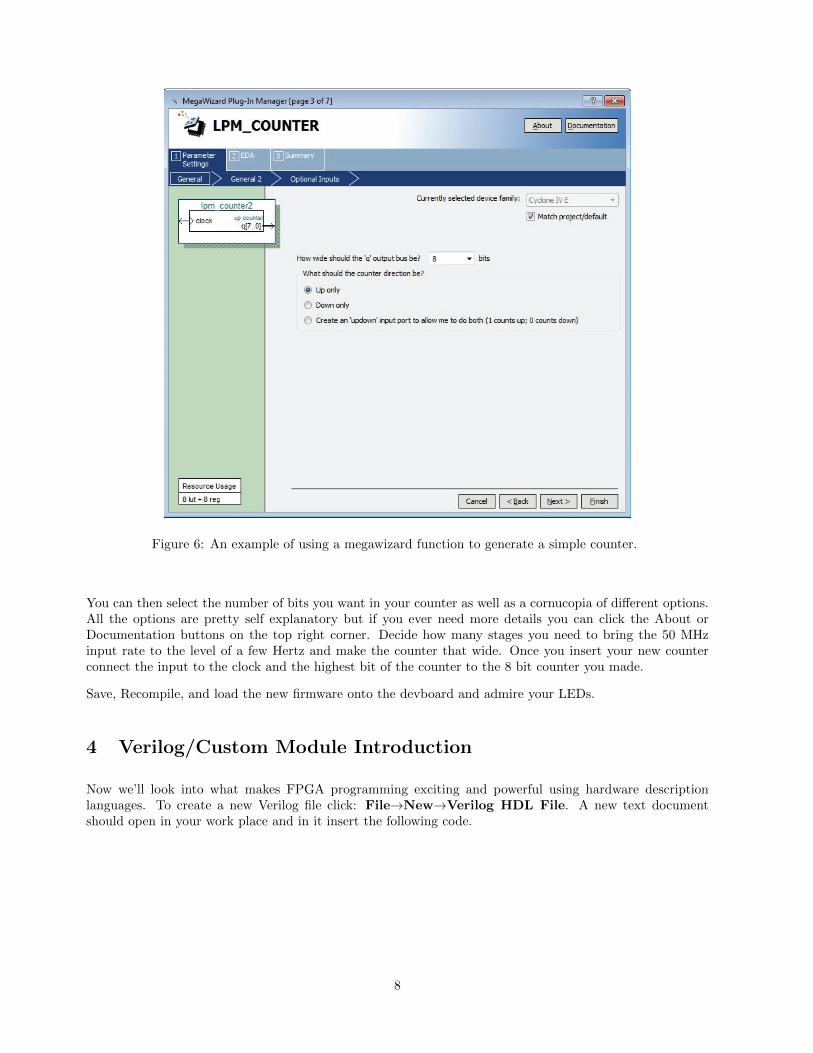
Figure 6: An example of using a megawizard function to generate a simple counter.
You can then select the number of bits you want in your counter as well as a cornucopia of different options.All the options are pretty self explanatory but if you ever need more details you can click the About orDocumentation buttons on the top right corner. Decide how many stages you need to bring the 50 MHzinput rate to the level of a few Hertz and make the counter that wide. Once you insert your new counterconnect the input to the clock and the highest bit of the counter to the 8 bit counter you made.
Save, Recompile, and load the new firmware onto the devboard and admire your LEDs.
4 Verilog/Custom Module Introduction
Now we’ll look into what makes FPGA programming exciting and powerful using hardware descriptionlanguages. To create a new Verilog file click: File→New→Verilog HDL File. A new text documentshould open in your work place and in it insert the following code.
8
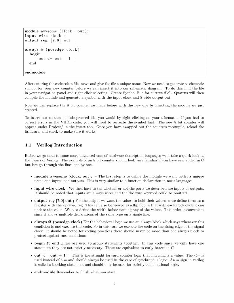
module awesome ( c lock , out ) ;input wire c l o ck ;output reg [ 7 : 0 ] out ;
always @ (posedge c l o ck )begin
out <= out + 1 ;end
endmodule
After entering the code select file→save and give the file a unique name. Now we need to generate a schematicsymbol for your new counter before we can insert it into our schematic diagram. To do this find the filein your navigation panel and right click selecting ”Create Symbol File for current file”. Quartus will thencompile the module and generate a symbol with the input clock and 8 wide output out.
Now we can replace the 8 bit counter we made before with the new one by inserting the module we justcreated.
To insert our custom module proceed like you would by right clicking on your schematic. If you had tocorrect errors in the VHDL code, you will need to recreate the symbol first. The new 8 bit counter willappear under Project/ in the insert tab. Once you have swapped out the counters recompile, reload thefirmware, and check to make sure it works.
4.1 Verilog Introduction
Before we go onto to some more advanced uses of hardware description languages we’ll take a quick look atthe basics of Verilog. The example of an 8 bit counter should look very familiar if you have ever coded in Cbut lets go through the lines one by one.
• module awesome (clock, out); - The first step is to define the module we want with its uniquename and inputs and outputs. This is very similar to a function declaration in most languages.
• input wire clock ; We then have to tell whether or not the ports we described are inputs or outputs.It should be noted that inputs are always wires and the the wire keyword could be omitted.
• output reg [7:0] out ; For the output we want the values to hold their values so we define them as aregister with the keyword reg. This can also be viewed as a flip flop in that with each clock cycle it canupdate the value. We also define the width before naming any of the values. This order is convenientsince it allows multiple declarations of the same type on a single line.
• always @ (posedge clock) For the behavioral logic we use an always block which says whenever thiscondition is met execute this code. So in this case we execute the code on the rising edge of the signalclock. It should be noted for coding practices there should never be more than one always block toprotect against race conditions.
• begin & end These are used to group statements together. In this code since we only have onestatement they are not strictly necessary. These are equivalent to curly braces in C.
• out <= out + 1 ; This is the straight forward counter logic that increments a value. The <= isused instead of a = and should always be used in the case of synchronous logic. An = sign in verilogis called a blocking statement and should only be used for strictly combinational logic.
• endmodule Remember to finish what you start.
9

There is obviously a lot more to learn about verilog but this is the bare minumum you need to get started.
4.2 State Machines
The last step is to introduce the most powerful coding technique for Verilog and other hardware descriptionlanguages: the Finite State Machine. In Verilog it is straight forward and easy to make a state machine bysomething like the following in your code: reg [1:0] State ;
As we discussed above this produces a register 2 bit value that can hold the state of our module. This canbe updated with different input conditions in always blocks like the example below:
module PrettyNeeto ( c lock , out ) ;input wire c l o ck ;output reg [ 7 : 0 ] out ;
reg [ 1 : 0 ] s t a t e ;
localparam f i r s t = 2 ’ b00 ;localparam second = 2 ’ b01 ;localparam th i r d = 2 ’ b10 ;localparam f our th = 2 ’ b11 ;
always @ (posedge c l o ck )begin
case ( s t a t e )f i r s t : begin
s t a t e <= second ;out <= 8 ’ b00001111 ;
endsecond : begin
s t a t e <= th i rd ;out <= 8 ’ b00111100 ;
endth i r d : begin
s t a t e <= four th ;out <= 8 ’ b11110000 ;
endf our th : begin
s t a t e <= f i r s t ;out <= 8 ’ b11000011 ;
enddefault : begin
s ta te<= f i r s t ;end
endcaseend
endmodule
The state variable can be updated in a synchronous block just like any other variable and can hold the stateof our module. In addition, this example uses local parameters which can be viewed as just helpful aliases tomake your code more readable. Try copying the above code into a module and editing it to make your ownLED pattern. You can do this by simply replacing the 8 bit counter you made with the new state machine
10

you define. You can always add more states to make more complex patterns and should feel free to do so.
Congratulations! you have the basics of FPGAs at your finger tips and have successfullycompleted an introduction to embedded systems.
5 Appendices
A Automatic Program Loading
You can store your program in a special non-volatile ROM on the DEO-Nano board so that it loads andstarts executing automatically whenever power is applied, with or without a computer connected. The stepsfor doing this are given on pp 143-150 of the DEO-Nano User Manual. If there is already a program stored,it will be necessary to erase it before storing a new one (p 149).
B Setting up USB Blaster
Setting up the USB Blaster on a windows machine can be a little tricky. The current version of QuartusII ( version 12.0 sp2 ) does not ship with the JTAG service correctly. To remedy this you can installthe Programmer independently off the Altera site. Once that is done you will have to install the driversmanually on Windows 7 by plugging in the board and finding it in the Device Manager: Right Click MyComputer - select manage - Then select the Device Manager Tab You should be able to find the deviceunder Other Devices simply right click on the icon and select Update Drivers. The drivers can be found inC:/Altera/13.0sp1/qprogramer/usb-blaster. (Was in C:/Altera/12.0sp2/quartus/usb-blaster.)
C Manually Assigning Pins
To manually assign pins in quartus II is not difficult but requires careful attention to detail and a lot oftyping. The first step is to define all the inputs and outputs that you are going to want to use. This is donein the top module. If its a schematic just insert inputs and outputs and label something unique and if its aHDL then simply define the inputs and outputs.
Once you have saved the top file you can go to Assignments→Pins.
With the pin planner you will see all the inputs and outputs you have on the left with the location Unas-signed. You can assign them to a pin by clicking on the location box and scrolling through the pins ortyping in the correct ones.
If you laid out the board yourself you will hopefully know the locations you want and if you forgot you canread the FPGA chip manual. Devboards usually have scripts to setup the pins like the DE0 NANO if theydon’t come with a script you can always find the pin locations/descriptions in the manual.
One can image this can be very tedious for an FPGA with greater than 100 pins so it is always good to seeif someone has already made a config file that you can edit.
11

Figure 7: Screenshot of the Device Manager with the USB Blaster plugged in but without drivers installed
References
[1] Altera, My First FPGA Design Tutorial, available at http://www.altera.com/literature/tt/tt_my_first_fpga.pdf.
[2] Terasic, DE0 Nano Manual, available at http://www.terasic.com.tw
12