Photoresponsive and Gas Sensing Field-Effect … · Photoresponsive and Gas Sensing Field-Effect...
9
Photoresponsive and Gas Sensing Field-Effect Transistors based on Multilayer WS 2 Nanoflakes Nengjie Huo 1 , Shengxue Yang 1 , Zhongming Wei 2 , Shu-Shen Li 1 , Jian-Bai Xia 1 & Jingbo Li 1 1 State Key Laboratory for Superlattices and Microstructures, Institute of Semiconductors, Chinese Academy of Sciences, P.O. Box 912, Beijing 100083, China, 2 Nano-Science Center & Department of Chemistry, University of Copenhagen, Universitetsparken 5, DK-2100 Copenhagen Ø, Denmark. The photoelectrical properties of multilayer WS 2 nanoflakes including field-effect, photosensitive and gas sensing are comprehensively and systematically studied. The transistors perform an n-type behavior with electron mobility of 12 cm 2 /Vs and exhibit high photosensitive characteristics with response time (t) of ,20 ms, photo-responsivity (R l ) of 5.7 A/W and external quantum efficiency (EQE) of 1118%. In addition, charge transfer can appear between the multilayer WS 2 nanoflakes and the physical-adsorbed gas molecules, greatly influencing the photoelectrical properties of our devices. The ethanol and NH 3 molecules can serve as electron donors to enhance the R l and EQE significantly. Under the NH 3 atmosphere, the maximum R l and EQE can even reach 884 A/W and 1.7 3 10 5 %, respectively. This work demonstrates that multilayer WS 2 nanoflakes possess important potential for applications in field-effect transistors, highly sensitive photodetectors, and gas sensors, and it will open new way to develop two-dimensional (2D) WS 2 -based optoelectronics. G raphene, the monolayer counterpart of graphite, has attracted extensive attention in recent years because of its unusual electrical, optical, magnetic and mechanical properties 1–4 . It displays an exceptionally high carrier mobility exceeding 10 6 cm 2 V 21 s 21 at 2 K and 15000 cm 2 V 21 s 21 at room temperature 5,6 , and the linear dispersion of the Dirac electrons near the K point makes graphene be used as photodetector with high operation frequencies 7 and ultrawide band operation 8 . However, the zero bandgap of graphene limits its applica- tions in optoelectronics, for example, field-effect transistors (FETs) based on graphene cannot be effectively switched off due to the high OFF-currents. In contrast, 2D transition metal dichalcogenides (TMDCs) with chemical formula MX 2 (M 5 Mo, W, Ga, etc. and X 5 S, Se or Te) possess sizable bandgaps 9,10 around 1–2 eV, which attracted widely interest due to their interesting physical properties and applications in nanoelectronics, sensing and photonics 11–16 . Particularly, the 2D TMDCs based FETs, photodetectors and gas sensors have been extensively studied. As one earliest TMDCs used in FETs, WSe 2 crystal 17 shows high mobility (.500 cm 2 V 21 s 21 ), ambipolar behavior and 10 4 on/off ratio at 60 K. Afterwards, mono or few-layer MoS 2 FETs with a back-gated 18 and top-gated configuration 19 are reported to exhibit an excellent on/off ratio (,10 8 ) and room-temperature mobility of . 200 cm 2 V 21 s 21 . Although the high photodetection performance, several problems such as very low responsivity (,10 22 A/W) and external quantum efficiency (0.1–0.2%) still remain with graphene photo- detectors 20,21 . Compared to graphene-based devices, photodetectors made from TMDCs thin layers can exhibit enhanced responsivity and selectivity. For example, a few-layer MoS 2 photodetector is demonstrated with improved responsivity (0.57 A/W) and fast photoresponse 11 (,70–110 ms), and the monolayer MoS 2 -based devices 22 show a maximum photoresponsivity of 880 A/W. Recently, 2D GaS and GaSe thin nanosheets are also reported as high performance photodetectors 13,14,23,24 . Moreover, TMDCs suggest opportunities in molecu- lar sensing applications due to the high surface-to-volume ratio. For instance, single and few-layer MoS 2 sheets have been demonstrated to be sensitive detectors for NO, NO 2 , NH 3 and triethylamine gas 25–28 . The detection mechanism is probably due to the n-doping or p-doping induced by the adsorbed gas molecular, changing the resistivity of the intrinsically n-doped MoS 2 . However, as a typical member of 2D TMDCs materials, WS 2 thin layers are less studied on their photoelectrical properties. Particularly, no research has been reported for the potential application of WS 2 in photodetector and gas sensors. Actually, WS 2 possesses some advantages compared to MoS 2 . For example, MoS 2 is usually procured from natural sources with no control over con- taminations. WS 2 exhibits higher thermal stability 29 and wider operation temperature range as lubricants 30 .A OPEN SUBJECT AREAS: PHOTONIC DEVICES ELECTRONIC MATERIALS ELECTRONIC DEVICES SENSORS Received 19 February 2014 Accepted 28 April 2014 Published 9 June 2014 Correspondence and requests for materials should be addressed to J.L. ([email protected]) SCIENTIFIC REPORTS | 4 : 5209 | DOI: 10.1038/srep05209 1
-
Upload
duonghuong -
Category
Documents
-
view
243 -
download
0
Transcript of Photoresponsive and Gas Sensing Field-Effect … · Photoresponsive and Gas Sensing Field-Effect...
Photoresponsive and Gas SensingField-Effect Transistors based onMultilayer WS2 NanoflakesNengjie Huo1, Shengxue Yang1, Zhongming Wei2, Shu-Shen Li1, Jian-Bai Xia1 & Jingbo Li1
1State Key Laboratory for Superlattices and Microstructures, Institute of Semiconductors, Chinese Academy of Sciences, P.O. Box912, Beijing 100083, China, 2Nano-Science Center & Department of Chemistry, University of Copenhagen, Universitetsparken 5,DK-2100 Copenhagen Ø, Denmark.
The photoelectrical properties of multilayer WS2 nanoflakes including field-effect, photosensitive and gassensing are comprehensively and systematically studied. The transistors perform an n-type behavior withelectron mobility of 12 cm2/Vs and exhibit high photosensitive characteristics with response time (t) of,20 ms, photo-responsivity (Rl) of 5.7 A/W and external quantum efficiency (EQE) of 1118%. In addition,charge transfer can appear between the multilayer WS2 nanoflakes and the physical-adsorbed gas molecules,greatly influencing the photoelectrical properties of our devices. The ethanol and NH3 molecules can serve aselectron donors to enhance the Rl and EQE significantly. Under the NH3 atmosphere, the maximum Rl andEQE can even reach 884 A/W and 1.7 3 105%, respectively. This work demonstrates that multilayer WS2nanoflakes possess important potential for applications in field-effect transistors, highly sensitivephotodetectors, and gas sensors, and it will open new way to develop two-dimensional (2D) WS2-basedoptoelectronics.
Graphene, the monolayer counterpart of graphite, has attracted extensive attention in recent years becauseof its unusual electrical, optical, magnetic and mechanical properties1–4. It displays an exceptionally highcarrier mobility exceeding 106 cm2 V21 s21 at 2 K and 15000 cm2 V21 s21 at room temperature5,6, and the
linear dispersion of the Dirac electrons near the K point makes graphene be used as photodetector with highoperation frequencies7 and ultrawide band operation8. However, the zero bandgap of graphene limits its applica-tions in optoelectronics, for example, field-effect transistors (FETs) based on graphene cannot be effectivelyswitched off due to the high OFF-currents. In contrast, 2D transition metal dichalcogenides (TMDCs) withchemical formula MX2 (M 5 Mo, W, Ga, etc. and X 5 S, Se or Te) possess sizable bandgaps9,10 around 1–2 eV,which attracted widely interest due to their interesting physical properties and applications in nanoelectronics,sensing and photonics11–16. Particularly, the 2D TMDCs based FETs, photodetectors and gas sensors have beenextensively studied. As one earliest TMDCs used in FETs, WSe2 crystal17 shows high mobility (.500 cm2 V21 s21),ambipolar behavior and 104 on/off ratio at 60 K. Afterwards, mono or few-layer MoS2 FETs with a back-gated18
and top-gated configuration19 are reported to exhibit an excellent on/off ratio (,108) and room-temperaturemobility of . 200 cm2 V21 s21. Although the high photodetection performance, several problems such as verylow responsivity (,1022 A/W) and external quantum efficiency (0.1–0.2%) still remain with graphene photo-detectors20,21. Compared to graphene-based devices, photodetectors made from TMDCs thin layers can exhibitenhanced responsivity and selectivity. For example, a few-layer MoS2 photodetector is demonstrated withimproved responsivity (0.57 A/W) and fast photoresponse11 (,70–110 ms), and the monolayer MoS2-baseddevices22 show a maximum photoresponsivity of 880 A/W. Recently, 2D GaS and GaSe thin nanosheets arealso reported as high performance photodetectors13,14,23,24. Moreover, TMDCs suggest opportunities in molecu-lar sensing applications due to the high surface-to-volume ratio. For instance, single and few-layer MoS2 sheetshave been demonstrated to be sensitive detectors for NO, NO2, NH3 and triethylamine gas25–28. The detectionmechanism is probably due to the n-doping or p-doping induced by the adsorbed gas molecular, changing theresistivity of the intrinsically n-doped MoS2. However, as a typical member of 2D TMDCs materials, WS2 thinlayers are less studied on their photoelectrical properties. Particularly, no research has been reported for thepotential application of WS2 in photodetector and gas sensors. Actually, WS2 possesses some advantagescompared to MoS2. For example, MoS2 is usually procured from natural sources with no control over con-taminations. WS2 exhibits higher thermal stability29 and wider operation temperature range as lubricants30. A
OPEN
SUBJECT AREAS:PHOTONIC DEVICES
ELECTRONIC MATERIALS
ELECTRONIC DEVICES
SENSORS
Received19 February 2014
Accepted28 April 2014
Published9 June 2014
Correspondence andrequests for materials
should be addressed toJ.L. ([email protected])
SCIENTIFIC REPORTS | 4 : 5209 | DOI: 10.1038/srep05209 1
recent calculation also shows that single layer WS2 has the potentialto outperform other 2D crystals in FETs applications due to itsfavorable bandstructure31, and the transistors based on chemicallysynthesized layered WS2 is also reported to exhibit 105 room tem-perature modulation and ambipolar behavior32.
In this paper, multilayer WS2 nanoflakes are exfoliated from thecommercially available WS2 crystals (Lamellae Co.) onto 300 nmSiO2/Si substrates using conventional mechanical exfoliation tech-nique. The multilayer WS2 nanoflakes transistors show excellentfield-effect properties with a high electron mobility of 12 cm2/Vsand high sensitive to red light (633 nm) with Rl (defined as thephotocurrent generated per unit power of the incident light on theeffective area) of 5.7 A/W and high EQE (defined as the number ofphoto-induced carriers detected per incident photons) of 1118%,indicating the 2D WS2 will be a new promising material for highperformance photodetectors. Moreover, the sensing of various gasmolecules on this transistor is preliminary investigated for the firsttime. We find strong response upon exposure to reducing gas ofethanol and NH3, which can serve as electron donors, enhancingn-type and conductivity of WS2 nanoflakes. On the contrary, theoxidizing gas of oxygen can act as electron acceptors to withdrawsubstantial electrons from the WS2 nanoflakes, depleting its n-typeand reducing the conductivity. We also observe the enhanced Rl andprolonged response to the reducing gas, caused by temporary chargeperturbation in the WS2 nanoflakes from the adsorbed electrondonors. Remarkably, the maximum Rl of the device can reach884 A/W under light illumination of 50 mW/cm2 at the NH3 atmo-sphere, which is 106 times higher than the first graphene-basedphotodetectors7 and 105 times higher than previous reports formonolayer MoS2 phototransistors33. Here, the excellent electrical,photosensitive and gas sensing properties of the multilayer WS2
nanoflakes transistors are studied systematically, suggesting greatpotential practical applications in FETs, photodetectors and gassensors.
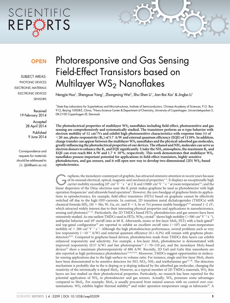
ResultsCharacterization of multilayer WS2 nanoflakes. Bulk WS2 is anindirect-bandgap (1.4 eV) semiconductor, but can turn into adirect-bandgap (2.1 eV) material when exfoliated into themonolayer state34. Each single plane of WS2 comprises a trilayercomposed of a tungsten layer sandwiched between two sulfurlayers in a trigonal prismatic coordination as shown in Figure 1a.The multilayer WS2 nanoflakes based transistors were fabricatedwith a coplanar electrode geometry by ‘‘gold-wire mask moving’’technique35,36. Through the AFM (Figure 1b and Figure S1) andSEM (Figure 1c) images of actual devices with SiO2 as bottomgating, the thickness of the WS2 nanoflakes is about 42 nm, andthe width and length of the channel are 20 mm and 15 mm,respectively. Figure 1d shows the schematic diagram of the device.EDX (Figure S2) results indicate the existence of S and W elementswith an atom ratio of 2 in the WS2 nanoflakes.
The first-order Raman spectra of the WS2 nanoflakes showed twooptical phonon modes at the Brillouin zone center (E1
2g(C) andA1g(C)) and one longitudinal acoustic mode at the M point(LA(M)). E1
2g(C) was an in-plane optical mode, A1g(C) corre-sponded to out-of-plane vibrations of the sulfur atoms, and the lon-gitudinal acoustic phonons LA(M) were in-plane collectivemovements of the atoms (Figure S3). Raman spectra of the WS2
nanoflakes were performed with the 532 nm laser excitations(Figure 1e). The first-order Raman peaks are identified at 175,356.5 and 420.6 cm21, which are attributed to the LA(M), E1
2g(C)and A1g(C) modes, respectively. Additional peaks correspond to thesecond-order Raman modes which are multiphonon combinationsof these first-order modes. Our Raman results for the multilayer WS2
nanoflakes agree well with the previous reports37–39.
Electrical properties under dark and light illumination. Owing tothe lack of dangling bonds, structural stability and high mobility40,2D TMDCs were promising materials for FETs. To evaluate the
Figure 1 | Characterization of the multilayer WS2 nanoflakes. (a) Primitive cell and three-dimensional schematic representation of a typical WS2
structure with the sulfur atoms in yellow and the tungsten atoms in purple. Atomic force microscopy (AFM) image (b) and scanning electron microscopy
(SEM) image (c) of the actual transistor based on multilayer WS2 nanoflakes. (d) Schematic diagram of the device. The thickness of WS2 nanoflakes is
42 nm. The width (W) and length (L) of the channel in the device is 15 mm and 20 mm, respectively. (e) Room-temperature Raman spectrum from the
multilayer WS2 nanoflakes, using the 532 nm laser.
www.nature.com/scientificreports
SCIENTIFIC REPORTS | 4 : 5209 | DOI: 10.1038/srep05209 2

electrical performance of the multilayer WS2 nanoflakes, the bottom-gated transistors on SiO2/Si were fabricated. Figure 2a and 2b showthe typical output and transfer characteristics respectively,performing an n-type behavior. According to the previousreports41,42, in the case of VG . VT and jVDSj = jVG 2 VTj, theFETs are turned on. The positive gate voltage (VG) can induce largeamounts of electrons in the interfaces between the WS2 nanoflakesand SiO2 substrate, and a conducting channel is created which allowsthe current to flow between the source and drain. The FETs operatelike a resistor and work at linear region, thus the source-drain current(IDS) can linearly depend of source-drain voltage (VDS) as shown inthe inset of Figure 2a. In this case, the IDS and VDS can satisfy the
formula IDS~WL
mCi VG{VTð ÞVDS, where L is channel length
(20 mm), W is channel width (15 mm), and Ci is the gatecapacitance which can be given by equation Ci 5 eoer/d, eo (8.85 3
10212 F/m) is vacuum dielectric constant, and er (3.9) and d(300 nm) are dielectric constant and thickness of SiO2,respectively. The field-effect carrier mobility (m) and thresholdvoltage (VT) of WS2 nanoflakes based FETs can be calculated fromthe linear region of the output properties by supplying the values ofIDS and VDS at different VG into the above equation. We get that VT 5
23.5 V, and the electrons mobility is up to 12 cm2/Vs. To estimatethe intrinsic doping level of the prepared WS2 nanoflakes, IDS at zero
VG was modeled as IDS~qn2DWm(VDS
L), where n2D is the 2D carrier
concentration, q is the electron charge. From the outputcharacteristics of WS2 nanoflakes (Figure 2a), n2D is extracted tobe ,1.4 3 1011 cm22. We have also performed Hall-effectmeasurements with four-probes on the WS2 nanoflakes toaccurately determine m and n2D, and the results are very similarwith the field-effect m and n2D (Figure S4).
The multilayer WS2 nanoflakes FETs were also illuminated withwhite light from LED and red light from red laser, and the outputcharacteristics of the devices are shown in Figure 2c and 2d, respect-
ively. The transfer characteristic curves under dark and light areshown in Figure 2e. The curves are obviously improved under bothwhite and red light illumination, indicating the photosensitive prop-erty to the visible light. As discussed above, our prepared WS2 nano-flakes perform n-type behavior with an intrinsic density of electronsof about 1.4 3 1011 cm22. The carriers density can be modulated bysupplying the electrical gating, which can be explained simply usingthe parallel-plate capacitor model. When positive VG is added on thebottom of dielectric (SiO2), much electrons will be induced in theinterface between WS2 nanoflakes and SiO2, serving as conductivechannel and increasing the drain current. In contrast, negative VG
will deplete the electrons in the interface and reduce the drain cur-rent. In addition, the increased VDS can increase the carrier driftvelocity and reduce the carrier transit time Tt (defined as Tt 5 L2/mVDS), thus contributing to the increased drain current (Figure 2eand 2f). Table 1 show the VT, m and n2D under dark and light illu-mination for the multilayer WS2 nanoflakes, which are extractedfrom the linear region of output characteristics. We found that theabsolute values of VT, m and n2D are all increased under light illu-mination. The photo-generated carriers contribute to the increasedelectrons density resulting in that larger negative voltage is needed todeplete them. The electron mobility (m) can be obtained from the
equation m~LIDS
LVG(
LWCiVDS
), the source drain current IDS and cur-
rent change between ON and OFF states are increased under light
illumination, leading to the increased slope of LIDS=LVG, and hence
enhancing the calculated mobility.
Photodetector based on WS2 nanoflakes. Few- or monolayer MoS2
was demonstrated as ultrasensitive photodetectors based on theprevious reports11,22,43. In contrast to the widely studied MoS2 usedfor photodetectors, little attention has been paid to the 2D WS2.According to the above analysis, the multilayer WS2 nanoflakescan response to the visible light especially the red light with
Figure 2 | Field effect of the multilayer WS2 nanoflakes. (a) Output characteristics of the transistor based on multilayer WS2 nanoflakes using Au/Au as
the drain/source electrodes. The inset is linear region at low source drain voltage. (b) Transfer characteristics of the device at a fixed VDS of 1 V on a log
scale (left y axis) and on a linear scale (right y axis). All measurements were performed in air at room temperature with the absence of light. Output
characteristics of the device with (c) white light (15 mW/cm2) from LEDs and (d) red light (633 nm, 15 mW/cm2) from red lasers. (e) Transfer
characteristics of the devices in dark and under light illumination. (f) Output characteristics of the devices in dark with VDS ranging from 0 to 3 V.
www.nature.com/scientificreports
SCIENTIFIC REPORTS | 4 : 5209 | DOI: 10.1038/srep05209 3
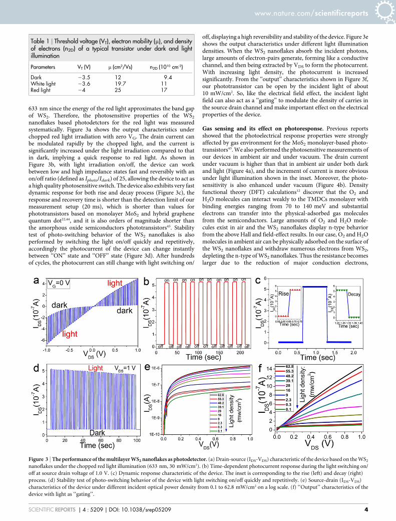
633 nm since the energy of the red light approximates the band gapof WS2. Therefore, the photosensitive properties of the WS2
nanoflakes based photodetctors for the red light was measuredsystematically. Figure 3a shows the output characteristics underchopped red light irradiation with zero VG. The drain current canbe modulated rapidly by the chopped light, and the current issignificantly increased under the light irradiation compared to thatin dark, implying a quick response to red light. As shown inFigure 3b, with light irradiation on/off, the device can workbetween low and high impedance states fast and reversibly with anon/off ratio (defined as Iphoto/Idark) of 25, allowing the device to act asa high quality photosensitive switch. The device also exhibits very fastdynamic response for both rise and decay process (Figure 3c), theresponse and recovery time is shorter than the detection limit of ourmeasurement setup (20 ms), which is shorter than values forphototransistors based on monolayer MoS2 and hybrid graphenequantum dot22,44, and it is also orders of magnitude shorter thanthe amorphous oxide semiconductors phototransistors45. Stabilitytest of photo-switching behavior of the WS2 nanoflakes is alsoperformed by switching the light on/off quickly and repetitively,accordingly the photocurrent of the device can change instantlybetween ‘‘ON’’ state and ‘‘OFF’’ state (Figure 3d). After hundredsof cycles, the photocurrent can still change with light switching on/
off, displaying a high reversibility and stability of the device. Figure 3eshows the output characteristics under different light illuminationdensities. When the WS2 nanoflakes absorb the incident photons,large amounts of electron-pairs generate, forming like a conductivechannel, and then being extracted by VDS to form the photocurrent.With increasing light density, the photocurrent is increasedsignificantly. From the ‘‘output’’ characteristics shown in Figure 3f,our phototransistor can be open by the incident light of about10 mW/cm2. So, like the electrical field effect, the incident lightfield can also act as a ‘‘gating’’ to modulate the density of carries inthe source drain channel and make important effect on the electricalproperties of the device.
Gas sensing and its effect on photoresponse. Previous reportsshowed that the photoelectrical response properties were stronglyaffected by gas environment for the MoS2 monolayer-based photo-transistors43. We also performed the photosensitive measurements ofour devices in ambient air and under vacuum. The drain currentunder vacuum is higher than that in ambient air under both darkand light (Figure 4a), and the increment of current is more obviousunder light illumination shown in the inset. Moreover, the photo-sensitivity is also enhanced under vacuum (Figure 4b). Densityfunctional theory (DFT) calculations12 discover that the O2 andH2O molecules can interact weakly to the TMDCs monolayer withbinding energies ranging from 70 to 140 meV and substantialelectrons can transfer into the physical-adsorbed gas moleculesfrom the semiconductors. Large amounts of O2 and H2O mole-cules exist in air and the WS2 nanoflakes display n-type behaviorfrom the above Hall and field-effect results. In our case, O2 and H2Omolecules in ambient air can be physically adsorbed on the surface ofthe WS2 nanoflakes and withdraw numerous electrons from WS2,depleting the n-type of WS2 nanoflakes. Thus the resistance becomeslarger due to the reduction of major conduction electrons,
Table 1 | Threshold voltage (VT), electron mobility (m), and densityof electrons (n2D) of a typical transistor under dark and lightillumination
Parameters VT (V) m (cm2/Vs) n2D (1010 cm-2)
Dark 23.5 12 9.4White light 23.6 19.7 11Red light 24 25 17
Figure 3 | The performance of the multilayer WS2 nanoflakes as photodetector. (a) Drain-source (IDS-VDS) characteristic of the device based on the WS2
nanoflakes under the chopped red light illumination (633 nm, 30 mW/cm2). (b) Time-dependent photocurrent response during the light switching on/
off at source drain voltage of 1.0 V. (c) Dynamic response characteristic of the device. The inset is corresponding to the rise (left) and decay (right)
process. (d) Stability test of photo-switching behavior of the device with light switching on/off quickly and repetitively. (e) Source-drain (IDS-VDS)
characteristics of the device under different incident optical power density from 0.1 to 62.8 mW/cm2 on a log scale. (f) ‘‘Output’’ characteristics of the
device with light as ‘‘gating’’.
www.nature.com/scientificreports
SCIENTIFIC REPORTS | 4 : 5209 | DOI: 10.1038/srep05209 4
corresponding to the reduced IDS. Upon light illumination in air,much electron-hole pairs generate and the density of electrons inthe WS2 nanoflakes is improved as discussed above. O2 and H2Omolecules as electron acceptors will have more electrons to accept,corresponding to more gas molecules in ambient can be adsorbedand deplete more electrons, leading to the decreased photosen-sitivity. Moreover, the photocurrent shows a strong dependence onlight intensity and the experimental data are fitted by a powerequation Iph 5 aPa, where a is scaling constant, and a is exponent.Under vacuum, the photocurrent displays a power dependence of,0.91 (function: Iph 5 0.26P0.91) as shown in Figure S5a, indicating asuperior photocurrent capability and a high efficiency of photo-generated charge carriers from the absorbed photons. However,the exponent a in air (function: Iph 5 0.52P0.73) shown in FigureS5b is smaller than that under vacuum, indicating the route of the
loss of the photo-exited carrier by the adsorbed O2 or H2O mole-cules in air. Similar phenomenon is also observed in MoS2-basedphototransistor43.
To further investigate the gas effect on the electrical and pho-tosensitive properties of the multilayer WS2 nanoflakes, the deviceswere placed in various gas environments during photoelectrical mea-surements. From the IDS 2 VDS characteristics (Figure 4c) and time-dependent photocurrent response at various gas atmospheres duringthe light switching on/off (Figure 4d), the WS2 nanoflakes canobviously response to the given gas molecules which play an import-ant and different roles in the conductivity and photosensitive prop-erties of the devices. Figure 4e summarizes the drain current underthese gas molecules both in dark and under light illumination, thedrain current of the device is decreased in O2 and air, but increased inethanol and NH3, compared to that under vacuum. The current
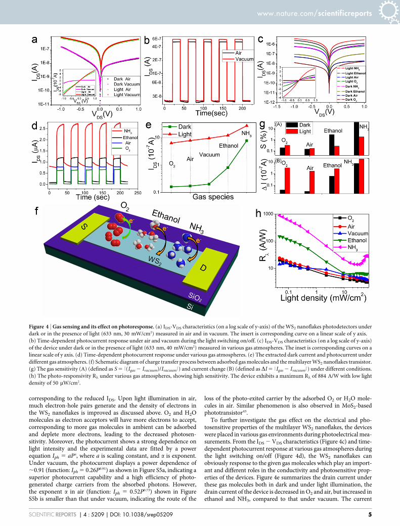
Figure 4 | Gas sensing and its effect on photoresponse. (a) IDS-VDS characteristics (on a log scale of y-axis) of the WS2 nanoflakes photodetectors under
dark or in the presence of light (633 nm, 30 mW/cm2) measured in air and in vacuum. The insert is corresponding curve on a linear scale of y axis.
(b) Time-dependent photocurrent response under air and vacuum during the light switching on/off. (c) IDS-VDS characteristics (on a log scale of y-axis)
of the device under dark or in the presence of light (633 nm, 40 mW/cm2) measured in various gas atmospheres. The inset is corresponding curves on a
linear scale of y axis. (d) Time-dependent photocurrent response under various gas atmospheres. (e) The extracted dark current and photocurrent under
different gas atmospheres. (f) Schematic diagram of charge transfer process between adsorbed gas molecules and the multilayer WS2 nanoflakes transistor.
(g) The gas sensitivity (A) (defined as S 5 | (Igas 2 Ivacuum)/Ivacuum | ) and current change (B) (defined as DI 5 | Igas 2 Ivacuum | ) under different conditions.
(h) The photo-responsivity Rl under various gas atmospheres, showing high sensitivity. The device exhibits a maximum Rl of 884 A/W with low light
density of 50 mW/cm2.
www.nature.com/scientificreports
SCIENTIFIC REPORTS | 4 : 5209 | DOI: 10.1038/srep05209 5
change is considered to result from the charge transfer between theWS2 nanoflakes and the adsorbed gas molecules as shown inFigure 4f. Once the vapor molecules come into contact with thesurface of WS2, the gas molecule is expected to be adsorbed andsubsequently change the charge carrier distribution in WS2 nano-flakes. O2 molecules can act as electron acceptors to accept electronsfrom WS2, leading to a reduction in overall conductivity. In contrast,ethanol and NH3 molecules, serving as electron donors, can donateelectrons to the WS2 nanoflakes, which enhance the total conductingelectrons density, resulting in the increased current. The gas sens-itivity is defined as S 5 j(Igas 2 Ivacuum)/Ivacuumj, where Igas is currentof the device in target gas, and Ivacuum is current under vacuum, VDS
are 1 V. Figure 4g (A) shows the gas sensitivity of the device underdifferent gas molecules. S is negative higher in O2 than that in air,because of the higher concentration of O2 acting as electron acceptorto deplete electrons. On the contrary, the ethanol and NH3 moleculescan act as electron donors to increase electrons in WS2, displaying apositive S. Particularly, the sensitivity of NH3 is much higher thanthat of other gas molecules, indicating the WS2 nanoflakes are moresensitive to NH3. Interestingly, we notice that the gas sensitivity ofethanol and NH3 measured in dark is higher than that under light,but lower for O2 and ambient air, the possible reason has beendescribed in Supporting Information. In addition, the current changeDI caused by gas adsorption represents the amounts of adsorbed gasmolecules to some extent shown in Figure 4g (B). Obviously, bothoxidizing (O2) and reducing (NH3, ethanol) gas molecules are easierto be adsorbed in the WS2 nanoflakes under light illumination com-pared to under dark, ascribed to the redundant photo-excited elec-trons or holes.
Furthermore, the exponent a in O2 (I , P0.62, Figure S6a) becomesvery small, indicating the photo-excited carriers are continuouslyconsumed by the adsorbed O2 molecules with increasing light den-sity. However, in ethanol (I , P1.02, Figure S6b) and NH3 (I , P2.5,Figure S6c), the a is significantly enhanced, implying a high effi-ciency of photo-generated charge carriers, attributed to that morereducing gas (ethanol or NH3) molecules can be adsorbed withincreasing incident light density and more electrons can transferfrom these adsorbates into the device. Thus, two physical processesupon light illumination including generation of photo-excited elec-trons and charge transfer from the adsorbed gas molecules can leadto the enhanced charge carrier density, demonstrating a high effi-ciency of photo-generated carriers. Figure 4h shows the Rl acquiredat different light power densities. At low illumination power density(50 mW/cm2) under NH3 atmosphere, the device reaches a high Rl of884 A/W and EQE of 1.7 3 105 %. The Rl shows a monotonousdecrease with increasing illumination intensity due to the saturationof trap states in the WS2 nanoflakes, which is similar with the MoS2-based photodetectors22. While, at high light powers under the ethanoland NH3 atmosphere, the Rl presents a slight increase trend withincreasing illumination intensity, further confirming that more redu-cing gas molecules can be adsorbed and transfer more electrons intothe device under high illumination power. Moreover, the presence ofgas molecules can also affect the dynamic response of the device,which is discussed in detail in Supporting Information (Figure S7).Briefly, unlike the single exponential formula for fitting the rise andfall photocurrent in other reports14,46, the dynamic response for riseand fall in our device under the reducing atmosphere (ethanol andNH3) can be perfectly fitted by double exponential formula, furtherindicating the existence of two physical mechanisms including rapidgeneration or recombination of photo-excited electron-hole pairsand gas adsorption or charge transfer process in the dynamic res-ponse to the light switching on/off.
DiscussionBased on the above experimental results, the multilayer WS2 nano-flakes exhibit n-type behavior with relatively large electron mobility
of 12 cm2/Vs, which is much higher than the CVD-grown monolayerWS2 (m 5 0.01 cm2/Vs) by three orders of magnitude47 and compar-able to the widely studied few- or monolayer MoS2 (m5 0.1–10 cm2/Vs)fabricated without high-k dielectrics19,47,48, but smaller than the top-gated transistors based on the monolayer MoS2 (.200 cm2/Vs) andWSe2 (,250 cm2/Vs) with high k-dielectrics which are studied morerecently19,49. According to the previous reports50–53, the mobility couldbe improved significantly by deposition of high-k dielectric, such asHfO2 (er 5 19), on the top of 2D materials (graphene or TMDCs)owing to dielectric screening of coulomb scattering on chargedimpurities. The contact resistance or Schottky barrier could alsoinfluence the mobility extraction, and the low contact resistancewould enhance the driven current and the electrons mobility byselecting the metal electrode with appropriate work function15.However, in our device, Schottky barrier existed in the Au-WS2
contacts from the non-linear characteristics of output curve. Thus,there is incredible room for improving the mobility of WS2 nano-flakes FETs by using high-k dielectric and optimizing the contactfabrication. Besides, the multilayer WS2 nanoflakes FTEs display verysmall on/off ratio of only 13 times, ascribed to the high off-statecurrent which is attributed to the large thickness of our WS2 nano-flakes. It is predicted that mono-or few-layer WS2 would exhibit highfield-effect on/off ratio through reducing the off-state current.Therefore, we also fabricated few-layer WS2 based FETs (FigureS8a). Through the transfer and output characteristics (Figure S8b–c),the few-layer WS2 FETs exhibit ambipolar properties, the electronand hole mobility are calculated to be 0.47 and 0.79 cm2/Vs, respect-ively, and the on/off ratio is significantly improved to be .104 attrib-uted to the very low off-state current (10211 A) which agrees wellwith our conjecture. Such results are different and showed higher on/off ratio but lower mobility of few-layer WS2 compared to the multi-layer WS2 nanoflakes. Further study about the optoelectronic prop-erties of few-layer WS2 TETs is necessary for the next step.
As discussed above, the incident light field like the electrical fieldcan also modulate the density of carries in the source drain channeland make the multilayer WS2 nanoflakes be used as ultrasensitivephotodetectors with switching on/off ratio of 25 and fast responsetime of 20 ms. Rl and EQE are critical parameters for evaluating thequality of photodetctors and large value of Rl and EQE correspondsto high light-sensibility. Rl and EQE can be expressed as Rl 5 Iph/PSand EQE 5 hcRl/el, where Iph is the photo-excited current; P is thelight power intensity; S is the effective illumination area; h is Planck’sconstant; c is the velocity of light; e is electron charge; and l is theexcitation wavelength. From our experimental results, under lightirradiation (633 nm) of 30 mW/cm2 with VDS of 1 V, the Rl andEQE are calculated to be 5.7 A/W and 1118%, respectively, which arethree orders of magnitude larger than the photodetectors reportedfor graphene or single-layer MoS2
7,33, and even comparable to thereported GaSe and GaS-based photodetctors13,14. The high Rl andEQE are due to a high surface ratio which causes an efficient adsorp-tion of photons. All of the optoelectronic parameters have beencompared with those of other 2D materials (Table S1), demonstrat-ing that the multilayer WS2 nanoflakes have great potential in optoe-lectronics and highly sensitive photodetectors.
Some theoretical calculations and experimental results about thegas sensing of graphene and MoS2-based transistors have beenreported to demonstrate high sensitive to various gases, and it ispointed out that O2 and H2O can act as electron acceptors, whereasNH3 and ethanol are donors27, 54–57. In our case, the WS2 nanoflakestransistors can also response to these given gas molecules. The sourcedrain current of the device is decreased in O2 and air and increased inethanol and NH3, attributed to the charge transfer between the WS2
nanoflakes and the adsorbed gas molecules, which makes WS2 nano-flakes can be used in gas sensors. In brief, the multilayer WS2 nano-flakes are very sensitive to reducing gases, especially NH3 molecules,but relatively poor sensitive to O2 molecules. Under light illumina-
www.nature.com/scientificreports
SCIENTIFIC REPORTS | 4 : 5209 | DOI: 10.1038/srep05209 6
tion, all the gas molecules can be further adsorbed due to theincreased electron-hole pairs, and the gas sensitivity is increasedfor O2, but decreased for ethanol and NH3. To our best of knowledge,this is a first report that may create much interest in further studyabout the gas sensing performance or the mutual influence with lightfor monolayer WS2 or other 2D materials.
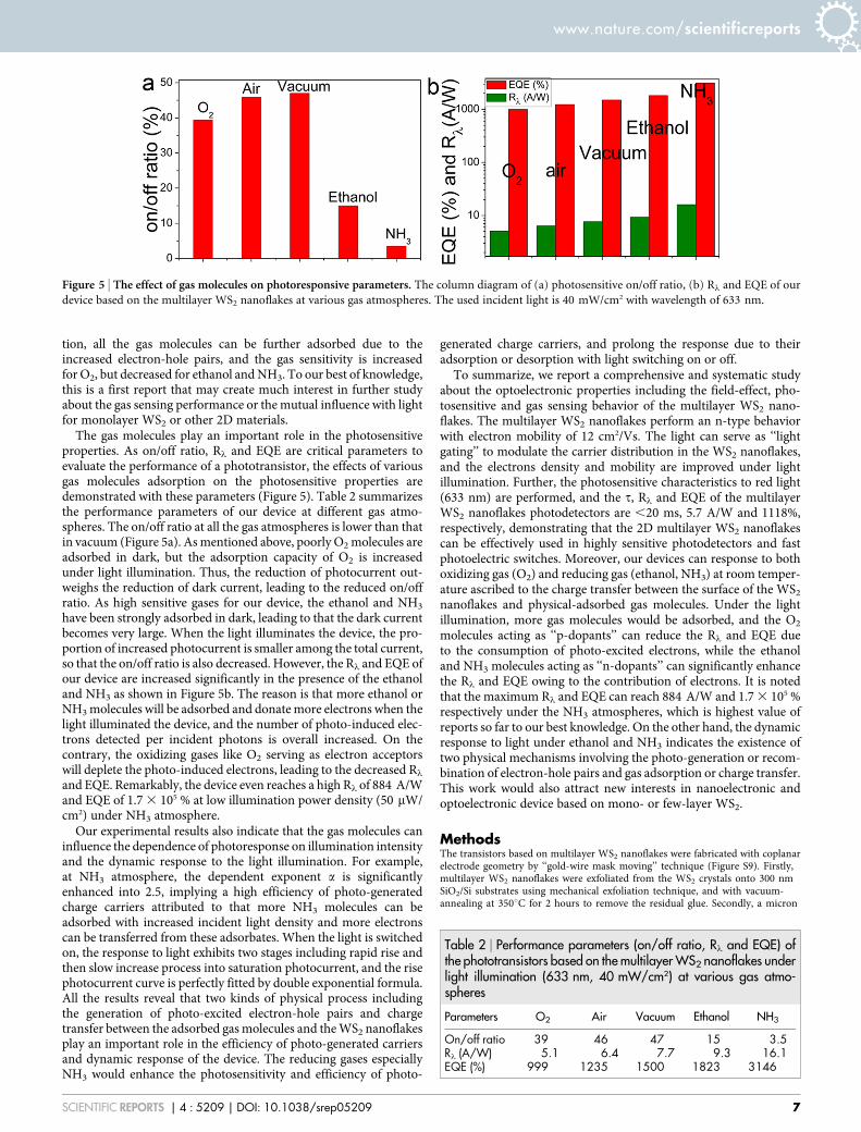
The gas molecules play an important role in the photosensitiveproperties. As on/off ratio, Rl and EQE are critical parameters toevaluate the performance of a phototransistor, the effects of variousgas molecules adsorption on the photosensitive properties aredemonstrated with these parameters (Figure 5). Table 2 summarizesthe performance parameters of our device at different gas atmo-spheres. The on/off ratio at all the gas atmospheres is lower than thatin vacuum (Figure 5a). As mentioned above, poorly O2 molecules areadsorbed in dark, but the adsorption capacity of O2 is increasedunder light illumination. Thus, the reduction of photocurrent out-weighs the reduction of dark current, leading to the reduced on/offratio. As high sensitive gases for our device, the ethanol and NH3
have been strongly adsorbed in dark, leading to that the dark currentbecomes very large. When the light illuminates the device, the pro-portion of increased photocurrent is smaller among the total current,so that the on/off ratio is also decreased. However, the Rl and EQE ofour device are increased significantly in the presence of the ethanoland NH3 as shown in Figure 5b. The reason is that more ethanol orNH3 molecules will be adsorbed and donate more electrons when thelight illuminated the device, and the number of photo-induced elec-trons detected per incident photons is overall increased. On thecontrary, the oxidizing gases like O2 serving as electron acceptorswill deplete the photo-induced electrons, leading to the decreased Rl
and EQE. Remarkably, the device even reaches a high Rl of 884 A/Wand EQE of 1.7 3 105 % at low illumination power density (50 mW/cm2) under NH3 atmosphere.
Our experimental results also indicate that the gas molecules caninfluence the dependence of photoresponse on illumination intensityand the dynamic response to the light illumination. For example,at NH3 atmosphere, the dependent exponent a is significantlyenhanced into 2.5, implying a high efficiency of photo-generatedcharge carriers attributed to that more NH3 molecules can beadsorbed with increased incident light density and more electronscan be transferred from these adsorbates. When the light is switchedon, the response to light exhibits two stages including rapid rise andthen slow increase process into saturation photocurrent, and the risephotocurrent curve is perfectly fitted by double exponential formula.All the results reveal that two kinds of physical process includingthe generation of photo-excited electron-hole pairs and chargetransfer between the adsorbed gas molecules and the WS2 nanoflakesplay an important role in the efficiency of photo-generated carriersand dynamic response of the device. The reducing gases especiallyNH3 would enhance the photosensitivity and efficiency of photo-
generated charge carriers, and prolong the response due to theiradsorption or desorption with light switching on or off.
To summarize, we report a comprehensive and systematic studyabout the optoelectronic properties including the field-effect, pho-tosensitive and gas sensing behavior of the multilayer WS2 nano-flakes. The multilayer WS2 nanoflakes perform an n-type behaviorwith electron mobility of 12 cm2/Vs. The light can serve as ‘‘lightgating’’ to modulate the carrier distribution in the WS2 nanoflakes,and the electrons density and mobility are improved under lightillumination. Further, the photosensitive characteristics to red light(633 nm) are performed, and the t, Rl and EQE of the multilayerWS2 nanoflakes photodetectors are ,20 ms, 5.7 A/W and 1118%,respectively, demonstrating that the 2D multilayer WS2 nanoflakescan be effectively used in highly sensitive photodetectors and fastphotoelectric switches. Moreover, our devices can response to bothoxidizing gas (O2) and reducing gas (ethanol, NH3) at room temper-ature ascribed to the charge transfer between the surface of the WS2
nanoflakes and physical-adsorbed gas molecules. Under the lightillumination, more gas molecules would be adsorbed, and the O2
molecules acting as ‘‘p-dopants’’ can reduce the Rl and EQE dueto the consumption of photo-excited electrons, while the ethanoland NH3 molecules acting as ‘‘n-dopants’’ can significantly enhancethe Rl and EQE owing to the contribution of electrons. It is notedthat the maximum Rl and EQE can reach 884 A/W and 1.7 3 105 %respectively under the NH3 atmospheres, which is highest value ofreports so far to our best knowledge. On the other hand, the dynamicresponse to light under ethanol and NH3 indicates the existence oftwo physical mechanisms involving the photo-generation or recom-bination of electron-hole pairs and gas adsorption or charge transfer.This work would also attract new interests in nanoelectronic andoptoelectronic device based on mono- or few-layer WS2.
MethodsThe transistors based on multilayer WS2 nanoflakes were fabricated with coplanarelectrode geometry by ‘‘gold-wire mask moving’’ technique (Figure S9). Firstly,multilayer WS2 nanoflakes were exfoliated from the WS2 crystals onto 300 nmSiO2/Si substrates using mechanical exfoliation technique, and with vacuum-annealing at 350uC for 2 hours to remove the residual glue. Secondly, a micron
Figure 5 | The effect of gas molecules on photoresponsive parameters. The column diagram of (a) photosensitive on/off ratio, (b) Rl and EQE of our
device based on the multilayer WS2 nanoflakes at various gas atmospheres. The used incident light is 40 mW/cm2 with wavelength of 633 nm.
Table 2 | Performance parameters (on/off ratio, Rl and EQE) ofthe phototransistors based on the multilayer WS2 nanoflakes underlight illumination (633 nm, 40 mW/cm2) at various gas atmo-spheres
Parameters O2 Air Vacuum Ethanol NH3
On/off ratio 39 46 47 15 3.5Rl (A/W) 5.1 6.4 7.7 9.3 16.1EQE (%) 999 1235 1500 1823 3146
www.nature.com/scientificreports
SCIENTIFIC REPORTS | 4 : 5209 | DOI: 10.1038/srep05209 7
gold-wire serving as a mask was fixed tightly on the top surface of WS2 nano-flakes, and then a pair of Au electrodes was deposited onto the substrate bythermal evaporation. To avoid the scattering of metallic atoms onto the side-faceof SiO2/Si substrates, the sides of the substrate were covered with tinfoil.Moreover, the distance between the thermal evaporation boat and the sample wasincreased to 15 cm and the deposition rate was controlled at around 0.5 A/s inorder to minimize the heat influence. Finally, by slightly removing the Au wiremask and tinfoil, the Au electrodes were fabricated and a micron size gap wasproduced between the two electrodes.
1. Geim, A. K. Graphene: Status and Prospects. Science 324, 1530–1534 (2009).2. Avouris, P., Chen, Z. & Perebeinos, V. Carbon-based electronics. Nat.
Nanotechnol. 2, 605–615 (2007).3. Rao, N. R., Sood, A. K., Subrahmanyam, K. S. & Govindaraj, A. Graphene: the new
two-dimensional nanomaterial. Angew. Chem. Int. Ed. 48, 7752–7777 (2009).4. Schwierz, F. Graphene transistors. Nat. Nanotechnol. 5, 487–496 (2010).5. Elias, D. C. et al. Dirac cones reshaped by interaction effects in suspended
graphene. Nature Phys. 7, 701–704 (2011).6. Geim, A. K. & Novoselov, K. S. The rise of graphene. Nature Mater. 6, 183–191
(2007).7. Xia, F., Mueller, T., Lin, Y., Valdes-Garcia, A. & Avouris, P. Ultrafast graphene
photodetector. Nat. Nanotechnol. 4, 839–843 (2009).8. Khan, M. A., Kuznia, J. N., Olson, D. T., Blasingame, M. & Bhattarai, A. R.
Schottky-barrier photodetector based on Mg-Doped P-type GaN films. Appl.Phys. Lett. 63, 2455–2456 (1993).
9. Wilson, J. A. & Yoffe, A. D. Transition metal dichalcogenides: discussion andinterpretation of observed optical, electrical and structural properties. Adv. Phys.18, 193–335 (1969).
10. Yoffe, A. D. Layer compounds. Annu. Rev. Mater. Sci. 3, 147–170 (1993).11. Tsai, D. S. et al. Few-Layer MoS2 with High Broadband Photogain and Fast
Optical Switching for Use in Harsh Environments. ACS Nano 7, 3905–3911(2013).
12. Tongay, S. et al. Broad-Range Modulation of Light Emission in Two-DimensionalSemiconductors by Molecular Physisorption Gating. Nano Lett. 13, 2831–2836(2013).
13. Hu, P. A. et al. Highly Responsive Ultrathin GaS Nanosheet Photodetectors onRigid and Flexible Substrates. Nano Lett. 13, 1649–1654 (2013).
14. Hu, P. A., Wen, Z., Wang, L., Tan, P. & Xiao, K. Synthesis of Few-Layer GaSeNanosheets for High Performance Photodetectors. ACS Nano 6, 5988–5994(2012).
15. Liu, W. et al. Role of Metal Contacts in Designing High-Performance Monolayern-Type WSe2 Field Effect Transistors. Nano Lett. 13, 1983–1990 (2013).
16. Mak, K., He, K., Shan, J. & Heinz, T. F. Control of valley polarization in monolayerMoS2 by optical helicity. Nat. Nanotechnol. 7, 494–498 (2012).
17. Podzorov, V., Gershenson, M. E., Kloc, C., Zeis, R. & Bucher, E. High-mobilityfield-effect transistors based on transition metal dichalcogenides. Appl. Phys. Lett.84, 3301–3303 (2004).
18. Ayari, A., Cobas, E., Ogundadegbe, O. & Fuhrer, M. S. Realization and electricalcharacterization of ultrathin crystals of layered transition-metal dichalcogenides.J. Appl. Phys. 101, 014507 (2007).
19. Radisavljevic, B., Radenovic, A., Brivio, J., Giacometti, V. & Kis, A. Single-layerMoS2 transistors. Nat. Nanotechnol. 6, 147–150 (2011).
20. Mueller, T., Xia, F. & Avouris, P. Graphene photodetectors for high-speed opticalcommunications. Nat. Photonics 4, 297–301 (2010).
21. Nair, R. R. et al. Fine Structure Constant Defines Visual Transparency ofGraphene. Science 320, 1308–1308 (2008).
22. Lopez-Sanchez, O., Lembke, D., Kayci, M. & Kis, A. Ultrasensitive photodetectorsbased on monolayer MoS2. Nat. Nanotechnol. 8, 497–501 (2013).
23. Xue, D. J. et al. Anisotropic Photoresponse Properties of Single Micrometer-SizedGeSe Nanosheet. Adv. Mater. 24, 4528–4533 (2012).
24. Late, D. J. et al. GaS and GaSe Ultrathin Layer Transistors. Adv. Mater. 24,3549–3554 (2012).
25. Li, H. et al. Fabrication of single- and multilayer MoS2 film-based field-effecttransistors for sensing NO at room temperature. Small 8, 63–67 (2012).
26. He, Q. et al. Fabrication of flexible MoS2 thin-film transistor arrays for practicalgas-sensing applications. Small 8, 2994–2999 (2012).
27. Late, D. J. et al. Sensing Behavior of Atomically Thin-Layered MoS2 Transistors.ACS Nano 7, 4879–4891 (2013).
28. Perkins, F. K. et al. Chemical Vapor Sensing with Monolayer MoS2. Nano Lett. 13,668–673 (2013).
29. Brainard, W. A. The Thermal Stability And Friction Of The Disulfides, Diselenides,And Ditellurides Of Molybdenum And Tungsten In Vacuum (1029 to 1026 torr).NASA, Washington, 1969.
30. Prasad, S. V., McDevitt, N. T. & Zabinski, J. S. Tribology of tungsten disulfide-nanocrystalline zinc oxide adaptive lubricant films from ambient to 500uC. Wear237, 186–196 (2000).
31. Leitao, L., Kumar, S. B., Yijian, O. & Jing, G. Performance Limits of MonolayerTransition Metal Dichalcogenide Transistors. IEEE Trans. Electron Devices 58,3042–3047 (2011).
32. Hwang, W. S. et al. Transistors with chemically synthesized layeredsemiconductor WS2 exhibiting 105 room temperature modulation and ambipolarbehavior. Appl. Phys. Lett. 101, 013107 (2012).
33. Yin, Z. et al. Single-layer MoS2 phototransistors. ACS Nano 6, 74–80 (2012).34. Kuc, A., Zibouche, N. & Heine, T. Influence of quantum confinement onthe
electronic structure of the transition metal sulfide TS2. Phys. Rev. B 83, 245213(2011).
35. Tang, Q. et al. Low Threshold Voltage Transistors Based on Individual Single-Crystalline Submicrometer-Sized Ribbons of Copper Phthalocyanine. Adv.Mater. 18, 65–68 (2006).
36. Tang, Q., Li, H., Liu, Y. & Hu, W. High-Performance Air-Stable n-TypeTransistors with an Asymmetrical Device Configuration Based on OrganicSingle-Crystalline Submicrometer/Nanometer Ribbons. J. Am. Chem. Soc. 128,14634–14639 (2006).
37. Elıas, A. L. et al. Controlled Synthesis and Transfer of Large-Area WS2 Sheets:From Single Layer to Few Layers. ACS Nano 7, 5235–5242 (2013).
38. Frey, G. L., Tenne, R., Matthews, M. J., Dresselhaus, M. S. & Dresselhaus, G.Optical Properties of MS2 (M 5 Mo, W) Inorganic Fullerene-like and NanotubeMaterial Optical Absorption and Resonance Raman Measurements. J. Mater. Res.13, 2412–2417 (1998).
39. Berkdemir, A. et al. Identification of Individual and Few Layers of WS2 UsingRaman Spectroscopy. Sci. Rep. 3, 1755 (2013).
40. Fivaz, R. & Mooser, E. Mobility of charge carriers in semiconducting layerstructures. Phys. Rev. 163, 743–755 (1967).
41. Sze, S. M. & Kwok, K. Ng. Physics Of Semiconductors Devices. John Wiley & Sons,Hoboken, 2006.
42. Carlos, G. M. & Marcio, C. S. MOSFET Modeling For Circuit Analysis And Design.World Scientific. Singapore, 2007.
43. Zhang, W. et al. High-Gain Phototransistors Based on a CVD MoS2 Monolayer.Adv. Mater. 25, 3456–3461 (2013).
44. Konstantatos, G. et al. Hybrid graphene-quantum dot phototransistors withultrahigh gain. Nat. Nanotechnol. 7, 363–368 (2012).
45. Jeon, S. et al. Gated three-terminal device architecture to eliminate persistentphotoconductivity in oxide semiconductor photosensor arrays. Nature Mater. 11,301–305 (2012).
46. Zhang, C. et al. High-performance photodetectors for visible and near-infraredlights based on individual WS2 nanotubes. Appl. Phys. Lett. 100, 243101 (2012).
47. Lee, Y. H. et al. Synthesis and Transfer of Single-Layer Transition Metal Disulfideson Diverse Surfaces. Nano Lett. 13, 1852–1857 (2013).
48. Novoselov, K. S. et al. Two-dimensional atomic crystals. Proc. Natl Acad. Sci. USA102, 10451–10453 (2005).
49. Fang, H. et al. High-performance single layered WSe2 p-FETs with chemicallydoped contacts. Nano Lett. 12, 3788–3792 (2012).
50. Jena, D. & Konar, A. Enhancement of carrier mobility in semiconductornanostructures by dielectric engineering. Phys. Rev. Lett. 98, 136805 (2007).
51. Konar, A., Fang, T. & Jena, D. Effect of high-k gate dielectrics on charge transportin graphene-based field effect transistors. Phys. Rev. B 82, 115452 (2010).
52. Newaz, A. K. M., Puzyrev, Y. S., Wang, B., Pantelides, S. T. & Bolotin, K. I. Probingcharge scattering mechanisms in suspended graphene by varying its dielectricenvironment. Nature Commun. 3, 734 (2012).
53. Chen, F., Xia, J., Ferry, D. K. & Tao, N. Dielectric screening enhanced performancein graphene FET. Nano Lett. 9, 2571–2574 (2009).
54. Leenaerts, O., Partoens, B. & Peeters, F. M. Adsorption of H2O, NH3, CO, NO2,and NO on graphene: A first-principles study. Phys. Rev. B 77, 125416 (2008).
55. Yuan, W. & Shi, G. Graphene-based gas sensors. J. Mater. Chem. A 1,10078–10091 (2013).
56. Schedin, F. et al. Detection of individual gas molecules adsorbed on graphene.Nature Mater. 6, 652–655 (2007).
57. Yue, Q., Shao, Z., Chang, S. & Li, J. Adsorption of gas molecules on monolayerMoS2 and effect of applied electric field. Nanoscale Res. Lett. 8, 425 (2013).
AcknowledgmentsThis work was supported by the National Natural Science Foundation of China under GrantNo.91233120 and the National Basic Research Program of China (2011CB921901).
Author contributionsN.H. and J.L. conceived the project. N.H. performed the measurements. Z.W. performedAFM measurements. S.Y., Z.W., S.S.L., J.B.X. and J.L. edited the manuscript. N.H. and J.L.wrote the manuscript. All authors have read the manuscript.
Additional informationSupplementary information accompanies this paper at http://www.nature.com/scientificreports
Competing financial interests: The authors declare no competing financial interests.
How to cite this article: Huo, N. et al. Photoresponsive and Gas Sensing Field-EffectTransistors based on Multilayer WS2 Nanoflakes. Sci. Rep. 4, 5209; DOI:10.1038/srep05209(2014).
www.nature.com/scientificreports
SCIENTIFIC REPORTS | 4 : 5209 | DOI: 10.1038/srep05209 8

This work is licensed under a Creative Commons Attribution-NonCommercial-ShareAlike 3.0 Unported License. The images in this article are included in thearticle’s Creative Commons license, unless indicated otherwise in the image credit;
if the image is not included under the Creative Commons license, users will need toobtain permission from the license holder in order to reproduce the image. To view acopy of this license, visit http://creativecommons.org/licenses/by-nc-sa/3.0/
www.nature.com/scientificreports
SCIENTIFIC REPORTS | 4 : 5209 | DOI: 10.1038/srep05209 9