Photonic Sintering of Silver Nanoparticles: Comparison of
18
8 Photonic Sintering of Silver Nanoparticles: Comparison of Experiment and Theory Jeff West, Michael Carter, Steve Smith and James Sears South Dakota School of Mines and Technology USA 1. Introduction Photonic sintering is a low thermal exposure sintering method developed to sinter nanoparticle thin films. The process involves using a xenon flash lamp to deliver a high intensity, short duration (< 1 ms), pulse of light to the deposited nanoparticles. Photonic sintering was developed by Nanotechnologies (now NovaCentrix) of Austin, Texas, and was first made public in 2006 (Schroder et al., 2006). As photonic sintering is a new technology it is also known as pulsed thermal processing (PTP) (Camm et al., 2006) and intense pulsed light (IPL) sintering (Kim et al., 2009). Conductive thin films composed of nanoparticle depositions, when exposed to a short pulse of high intensity light, are transformed into functional printed circuits. The printed circuits can be tailored for use as flexible circuit boards, RFID tags, flat panel displays (Carter & Sears, 2007), photovoltaics, or smart packaging (Novacentrix, 2009). One of the primary advantages of the method is that the high intensity pulse of light produces minimal damage on low temperature substrates. This allows the nanoparticles to be deposited and cured on a high variety of low temperature substrates such as cloth, paper, and Mylar (Carter & Sears, 2007; Farnsworth, 2009). Another advantage of using photonic curing is the speed at which nanoparticle depositions can be sintered. Rather than spending hours in an oven or programming a laser to follow the deposition path, the photonic curing process can sinter large areas (~ 200 cm 2 per 10 cm long lamp) in < 2 ms (Novacentrix 2009). One of the main objectives of the work reported here was to determine the effectiveness of photonic sintering of silver nanoparticle depositions. This was done by measuring the densification of silver nanoparticles films following photonic sintering. The absorption of light emitted by a flash lamp for varying thicknesses of silver nanoparticle layers was also measured. To determine the amount and depth of sintering, SEM images were taken of a cross section of a sintered film. To better understand the process through which the nanoparticles are sintered, we calculate the absorption of the light emitted by the flash lamp by the silver nanoparticle film using the Bruggeman effective medium theory. Using the heat transfer software package Fluent™ to model the temperature profile of the films during and following sintering, we propose a model for the photonic process. www.intechopen.com
Transcript of Photonic Sintering of Silver Nanoparticles: Comparison of
8
Photonic Sintering of Silver Nanoparticles: Comparison of
Experiment and Theory
Jeff West, Michael Carter, Steve Smith and James Sears South Dakota School of Mines and Technology
USA
1. Introduction
Photonic sintering is a low thermal exposure sintering method developed to sinter
nanoparticle thin films. The process involves using a xenon flash lamp to deliver a high
intensity, short duration (< 1 ms), pulse of light to the deposited nanoparticles. Photonic
sintering was developed by Nanotechnologies (now NovaCentrix) of Austin, Texas, and was
first made public in 2006 (Schroder et al., 2006). As photonic sintering is a new technology it
is also known as pulsed thermal processing (PTP) (Camm et al., 2006) and intense pulsed
light (IPL) sintering (Kim et al., 2009). Conductive thin films composed of nanoparticle
depositions, when exposed to a short pulse of high intensity light, are transformed into
functional printed circuits. The printed circuits can be tailored for use as flexible circuit
boards, RFID tags, flat panel displays (Carter & Sears, 2007), photovoltaics, or smart
packaging (Novacentrix, 2009). One of the primary advantages of the method is that the
high intensity pulse of light produces minimal damage on low temperature substrates. This
allows the nanoparticles to be deposited and cured on a high variety of low temperature
substrates such as cloth, paper, and Mylar (Carter & Sears, 2007; Farnsworth, 2009). Another
advantage of using photonic curing is the speed at which nanoparticle depositions can be
sintered. Rather than spending hours in an oven or programming a laser to follow the
deposition path, the photonic curing process can sinter large areas (~ 200 cm2 per 10 cm long
lamp) in < 2 ms (Novacentrix 2009).
One of the main objectives of the work reported here was to determine the effectiveness of
photonic sintering of silver nanoparticle depositions. This was done by measuring the
densification of silver nanoparticles films following photonic sintering. The absorption of
light emitted by a flash lamp for varying thicknesses of silver nanoparticle layers was also
measured. To determine the amount and depth of sintering, SEM images were taken of a
cross section of a sintered film. To better understand the process through which the
nanoparticles are sintered, we calculate the absorption of the light emitted by the flash lamp
by the silver nanoparticle film using the Bruggeman effective medium theory. Using the
heat transfer software package Fluent™ to model the temperature profile of the films during
and following sintering, we propose a model for the photonic process.
www.intechopen.com
Sintering – Methods and Products 174
2. Photonic sintering overview
Photonic sintering was first introduced at the 2006 NSTI Nanotechnology Conference and
Trade Show (Schroder et al., 2006). It was developed by NovaCentrix for the purpose of
rapidly sintering metal nanoparticle based films (Schroder et al., 2006). The technology
allows the nanoparticles to sinter without significantly raising the temperature of the
substrate. This is accomplished by using a flash lamp. Two main parameters control the
degree of sintering: the intensity of the lamp and the duration of the light pulse. The flash
lamp is held between 0.5 cm to 20 cm above the deposition and an intense current is run
through the flash lamp (Novacentrix, 2007). Due to this intense current, the xenon flash
lamp issues a high intensity, broad spectrum pulse of light. This pulse of light is absorbed
by the nanoparticles, which heats them to such a degree that they sinter into a single
component.
Because photonic sintering has a minimal effect on the substrate, it enables nanoparticle
films to be cured on low temperature substrates such as paper, Mylar, and PET. In addition
to allowing low temperature substrates to be used, the speed at which the films are sintered
allows the use of inks which would oxidize if sintered over long periods of time using
traditional methods, such as copper (Novacentrix, 2009; Schroder 2006). Both of these
advantages allow printed electronics manufacturers to reduce the cost of production by
using lower cost substrates and less expensive inks.
The Novacentrix PCS-1100 Photonic Curing System is a research and development model in
use at South Dakota School of Mines & Technology (SDSM&T). The PCS-1100 has a pulse
duration that can be set from 35 ┤s to 1000 ┤s (Novacentrix, 2007). The voltage of the flash
lamp (which controls the intensity and spectral distribution of the lamp) can also be
adjusted with a maximum operational voltage of 4000V (Novacentrix, 2007). The PulseForge
3100 is a production model (currently in operation at Oak Ridge National Laboratory) that
can be incorporated with a roll-to-roll production system or a conveyor belt to sinter
continuous or discrete items (Novacentrix, 2009).
During the development of photonic sintering, three basic assumptions were considered for
sintering nanoparticles: (i) nanoparticles are predominantly black, they should absorb light
very well (Schroder, 2006), (ii) once light is absorbed by the nanoparticles, due to their high
surface area to mass ratio, the nanoparticles would heat easily and sinter quickly, and (iii) as
nanoparticle films are very thin, they would not retain heat very well and cool rapidly,
minimizing damage to the substrate. Photonic sintering has been shown to sinter conductive
nanoparticle metals (e.g., silver, gold, and copper) as well as dielectric nanoparticles made of
alumina, zirconia, barium titanate, and mica, as well as the soft magnetic materials cobalt,
ferrite and iron-nickel permalloy (Carter & Sears, 2007).
A comparison of the resistivities obtained using furnace, laser, and photonic sintering was
reported by Carter and Sears (Carter & Sears, 2007). For the comparison, two different silver
inks were used. One ink was based on the AgSt2 Novacentrix 25 nm diameter silver
nanoparticles and the other ink was composed of UT Dot 7 nm diameter silver
nanoparticles. The inks were deposited into 1 cm2 pads and sintered using various furnace
temperatures, laser fluences, and flash lamp voltages. The resistivities were then measured
and the lowest values obtained for each method. The lowest resistivities were found using
www.intechopen.com
Photonic Sintering of Silver Nanoparticles: Comparison of Experiment and Theory 175
the following settings for each method. The furnace sintering was done at a temperature of
500°C for two hours. The laser sintering was done using a laser fluence of 2800 J/cm2. The
photonic curing was done using a lamp voltage of 1200V with a pulse length of 900 ┤s. The
lowest surface resistivity for each method is shown in Table 1. The measurements showed
that the resistivity of the photonically sintered silver was comparable to the resistivity of the
oven and laser sintered silver, and that smaller nanoparticles approach bulk silver
resistivities after photonic or oven sintering.
Material Sintering Method
Resistivity (μΩ-cm)
UT Dot (7 nm silver) Furnace 2.1 ± 0.9
Photonic 2.8 ± 0.8
AgSt2 (Novacentrix 25 nm silver) Furnace 3.8 ± 0.3
Laser 5.3 ± 0.3
Photonic 7.9 ± 0.5
Bulk Silver 1.59
Table 1. Table comparing resistivities obtained using different sintering methods for two
silver nanoparticle based inks.
3. Experimental results
After observing the comparisons to traditional sintering methods, experiments were run to
gain insight into the process by which particles are sintered during photonic curing. The
densification as a function of the flash lamp voltage and pulse duration was measured to
determine the effects of those parameters. Depositions of varying thickness were tested
using a UV-Vis spectrometer to measure the absorption of the depositions in the wavelength
region produced by the flash lamp. Finally, SEM images were taken of the cross section of a
thick sintered sample to determine the depth and amount of sintering in the deposition.
3.1 Parametric study of densification
We measured the densification of silver nanoparticles as a function of the pulse duration
and flash lamp voltage to find the optimal settings to sinter V2 silver ink. The V2 silver ink
consists of Novacentrix 25 nm silver nanoparticles suspended in DMA. The measurements
also allow a determination of the effect of lamp voltage and pulse duration on the sintering
process.
The process of measuring the densification began by finding the volume fraction of
nanoparticles in the deposition prior to sintering. This was accomplished by weighing a
clean glass slide and then depositing V2 ink in a square pattern on the slide. The thickness of
the deposition was then measured using a Zeiss Imager M1M microscope. The deposition
thickness was determined by focusing on the surface of the glass slide and then again on the
surface of the deposition. The focal distances were then compared to find the thickness of
www.intechopen.com
Sintering – Methods and Products 176
the deposition. The glass slide with the deposition was then weighed again to find the total
mass. The area and thickness of the deposition gave the total volume of the deposition and
from the weight measurements the mass of the deposition was also known. The mass of the
deposition was then divided by the density of silver to find the volume of the deposited
silver. The calculated volume of the silver was then divided by the volume of the deposition
to find the volume fraction of the silver in the deposition. The volume fraction of silver in
the deposition was calculated to be 36% using this method with a density of the deposition
being 3.8 g/cm3.
After finding the volume fraction of the silver in the deposition prior to sintering, the next
step was to deposit the material and measure the volume prior to and after sintering to
determine the densification of the deposition. This was accomplished by depositing V2
silver ink in a 3 mm by 10 mm pad on a glass slide. The thickness of the deposition was
measured using the Zeiss Imager M1M microscope. The deposition was then placed into the
photonic curing system and sintered. The thickness of the deposition was then measured
again. As the thickness was the only dimension to change during the sintering process the
change in the volume was found. As the mass stayed approximately constant after sintering,
the density of the deposition and volume fraction of silver in the deposition were then
calculated. This process was completed ten times for each setting on the photonic curing
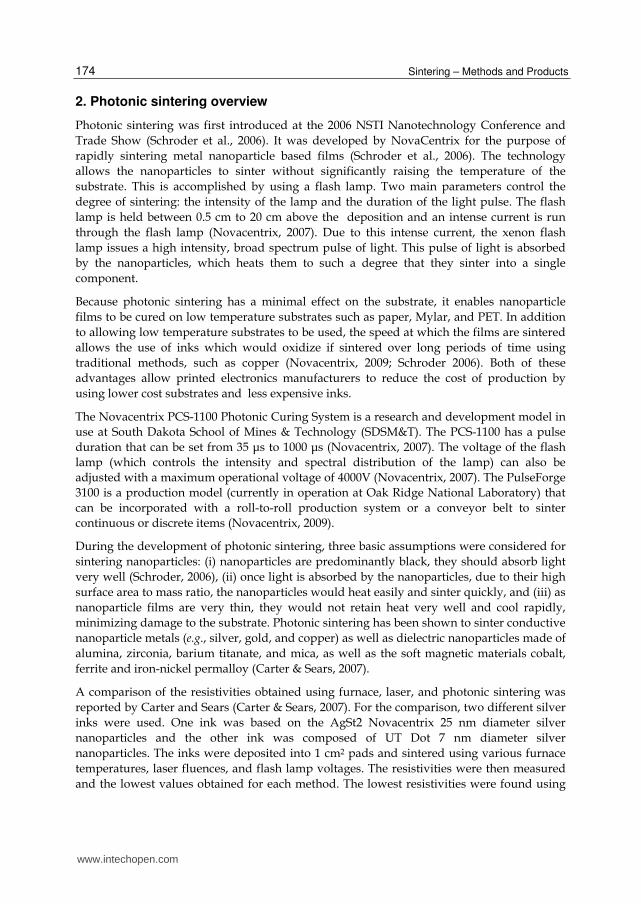
system to obtain an adequate sampling size. The results are shown in Figure 1.
Fig. 1. Graph of Sintered Density vs. Flash Lamp Voltage.
Figure 1 shows that there is a definite optimum voltage setting for the photonic curing of the
silver depositions tested. As the density of bulk silver is 10.6 g/cm3, the average density
using settings of 900 ┤s and 1200V of 8.89 g/cm3, gives a volume fraction of 83.87% for the
sintered silver. Figure 1 also shows that a longer pulse length produces a denser deposition
than a shorter pulse. Using flash lamp voltages above 1600V the depositions cracked and
experienced blow off due to the high intensity of the light. This was taken as an upper limit
to the voltages that can be used to sinter silver films using these pulse lengths.
3.00
4.00
5.00
6.00
7.00
8.00
9.00
10.00
800 1000 1200 1400 1600
Den
sit
y (
g/c
m3)
Voltage (V)
300 μs
600 μs
900 μs
www.intechopen.com
Photonic Sintering of Silver Nanoparticles: Comparison of Experiment and Theory 177
3.2 Measurement of UV-vis spectrum absorption
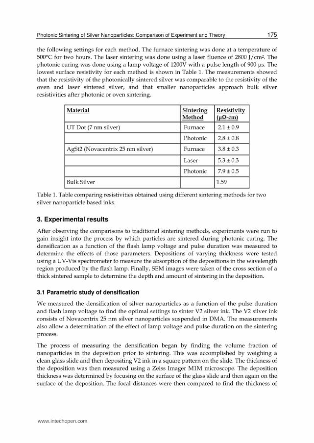
To find which wavelengths and how much of the light output by the flash lamp are
absorbed by different thicknesses of silver depositions, measurements of the absorption
were made by a HP 8452A Diode Array Spectrophotometer. These measurements allowed
us to determine the thickness of the silver deposition beyond which the light will no longer
penetrate. To make these measurements, depositions were made on a quartz slide to
minimize absorption and scattering effects from the substrate. The depositions were made
using the GPD aerosol jet system to deposit V2 silver in 1 cm2 pads. Thicknesses of 1.0, 3.1,
and 5.0 ┤m were measured using the Zeiss Imager M1M microscope and taken to the HP
8452A Diode Array Spectrophotometer for the absorption measurements. The
spectrophotometer takes a measurement of the absorption every 2 nm in wavelength, from
190 to 820 nm. The absorption is found by sending a pulse of light through the deposition
and substrate to a sensor on the other side. The absorption is measured as the amount of
light that does not reach the sensor. The spectrophotometer gives the results as the
absorbance. The absorption is found using the equation
畦 = 岫な − など貸銚岻 ∗ などど, (1)
where 畦 is the absorption and 欠 is the absorbance (Skoog, 1998). The results of the
measurements are shown in Figure 2.
Fig. 2. Absorption vs. Wavelength for different thicknesses of V2 silver depositions.
Figure 2 shows that there is strong absorption of the light by the silver deposition at
operational thicknesses. There is a drop in the absorption resulting in a minimum
absorption at 322 nm. There is near total absorption of the light using the 3.1 ┤m thickness
with the absorption after the minimum averaging 99%. There is complete absorption of the
light for the 5.0 ┤m thickness. This indicates that if there is any sintering of silver beyond
that thickness then it is due to thermal effects as there would be no light to impart energy to
the deposition at that depth. The absorption measurements do not show the plasmon
50.00
60.00
70.00
80.00
90.00
100.00
190 390 590 790
Ab
sorp
tio
n %
Wavelength (nm)
5.0 µm
3.1 µm
1.0 µm
www.intechopen.com
Sintering – Methods and Products 178
resonance peak that has been observed in silver nanoparticles suspended in solution (Chen
et al., 2004; Hutter et al., 2001; Lim et al., 2005). This indicates that the absorption for silver
nanoparticle films with volume fractions of 30% or higher of silver, more closely mimic the
absorption properties of bulk silver than of nanoparticle silver. Figure 2 also shows that the
V2 silver absorbs the light strongly in the visible portion of the spectrum which is the area
where bulk silver reflects a majority of the light. These measurements show that for the UV
and visible spectrums of light the V2 silver consistently absorbs a majority of the light
output from the lamp allowing photonic sintering to take place.
3.3 SEM Imaging of microstructure
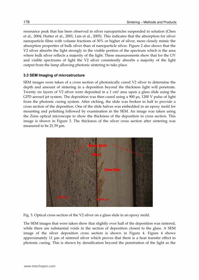
SEM images were taken of a cross section of photonically cured V2 silver to determine the
depth and amount of sintering in a deposition beyond the thickness light will penetrate.
Twenty six layers of V2 silver were deposited in a 1 cm2 area upon a glass slide using the
GPD aerosol jet system. The deposition was then cured using a 900 ┤s, 1200 V pulse of light
from the photonic curing system. After etching, the slide was broken in half to provide a
cross section of the deposition. One of the slide halves was embedded in an epoxy mold for
mounting and polishing followed by examination in the SEM. An image was taken using
the Zeiss optical microscope to show the thickness of the deposition in cross section. This
image is shown in Figure 3. The thickness of the silver cross section after sintering was
measured to be 21.59 ┤m.
Fig. 3. Optical cross section of the V2 silver on a glass slide in an epoxy mold.
The SEM images that were taken show that slightly over half of the deposition was sintered,
while there are substantial voids in the section of deposition closest to the glass. A SEM
image of the silver deposition cross section is shown in Figure 4. Figure 4 shows
approximately 11 ┤m of sintered silver which proves that there is a heat transfer effect in
photonic curing. This is shown by densification beyond the penetration of the light as the
www.intechopen.com
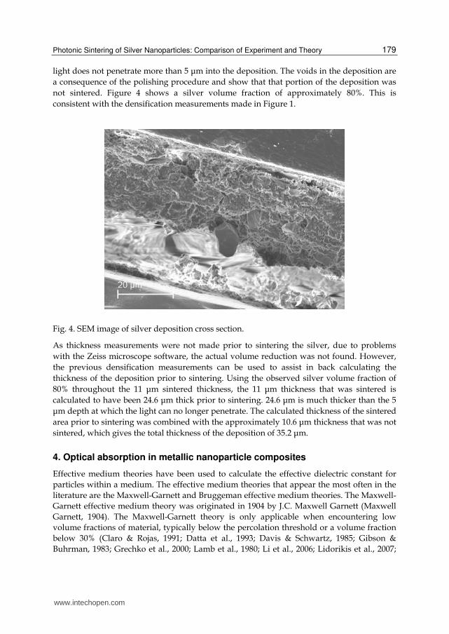
Photonic Sintering of Silver Nanoparticles: Comparison of Experiment and Theory 179
light does not penetrate more than 5 ┤m into the deposition. The voids in the deposition are
a consequence of the polishing procedure and show that that portion of the deposition was
not sintered. Figure 4 shows a silver volume fraction of approximately 80%. This is
consistent with the densification measurements made in Figure 1.
Fig. 4. SEM image of silver deposition cross section.
As thickness measurements were not made prior to sintering the silver, due to problems
with the Zeiss microscope software, the actual volume reduction was not found. However,
the previous densification measurements can be used to assist in back calculating the
thickness of the deposition prior to sintering. Using the observed silver volume fraction of
80% throughout the 11 ┤m sintered thickness, the 11 ┤m thickness that was sintered is
calculated to have been 24.6 ┤m thick prior to sintering. 24.6 ┤m is much thicker than the 5
┤m depth at which the light can no longer penetrate. The calculated thickness of the sintered
area prior to sintering was combined with the approximately 10.6 ┤m thickness that was not
sintered, which gives the total thickness of the deposition of 35.2 ┤m.
4. Optical absorption in metallic nanoparticle composites
Effective medium theories have been used to calculate the effective dielectric constant for
particles within a medium. The effective medium theories that appear the most often in the
literature are the Maxwell-Garnett and Bruggeman effective medium theories. The Maxwell-
Garnett effective medium theory was originated in 1904 by J.C. Maxwell Garnett (Maxwell
Garnett, 1904). The Maxwell-Garnett theory is only applicable when encountering low
volume fractions of material, typically below the percolation threshold or a volume fraction
below 30% (Claro & Rojas, 1991; Datta et al., 1993; Davis & Schwartz, 1985; Gibson &
Buhrman, 1983; Grechko et al., 2000; Lamb et al., 1980; Li et al., 2006; Lidorikis et al., 2007;
www.intechopen.com
Sintering – Methods and Products 180
Stroud & Pan, 1978; Wang et al., 2005; Yannopapas, 2006). However, other papers have
demonstrated that the Maxwell-Garnett effective medium theory will work for higher
volume fractions (Fu et al., 1993; Mallet et al., 2005). The Maxwell-Garnett dielectric function
is defined by the expression:
悌貸悌弐悌袋態悌弐 = 血銚 悌尼貸悌弐悌尼袋態悌弐, (2)
where ε is the dielectric function of the effective medium, εa is the dielectric function of the particles in the medium, εb is the dielectric function of the medium, and fa is the volume fraction of the particles contained in the medium (Aspnes, 1982).
The Bruggeman effective medium approximation was formulated in 1935 by D.A.G.
Bruggeman (Bruggeman, 1935). Unlike the Maxwell-Garnett model the Bruggeman model
does not have a preference toward the embedded particle or the medium, the Bruggeman
model treats the inclusions and medium equally (Aspnes, 1982; Landauer, 1978). The
Bruggeman model has been used to calculate the dielectric constant of particles embedded
in materials and compared with the measured values (Brosseau, 2002; Chen, L.Y. & Lynch,
1987; Mendoza-Galván et al., 1994; Rousselle et al., 1993). The Bruggeman model has also
been modified to better model the dielectric constant of nonlinear media and different
shaped particles (Goncharenko, 2003; Pellegrini 2001). The Bruggeman dielectric function
has been shown to work well with higher volume fractions (Bohren & Huffman, 1983;
Bruggeman, 1935). The Bruggeman dielectric function is defined by the expression:
血銚 悌尼貸悌悌尼袋態悌 + 血長 悌弐貸悌悌弐袋態悌 = ど, (3)
where ε is the dielectric function of the effective medium, εa is the dielectric function of the
particles in the medium, εb is the dielectric function of the medium, fa is the volume fraction
of the particles contained in the medium, and fb is the volume fraction of the particles
contained in the medium (Aspnes, 1982). Once the average dielectric function is found, the
imaginary portion of the refractive index and the absorption coefficient for the effective
medium can be calculated by the expression:
糠嫗 = 替訂賃碇 , (4)
where k is the imaginary part of the refractive index and ┣ is the wavelength of light (Skoog
et al., 1998). From this, using the Beer-Lambert law (Skoog et al., 1998), the absorption
spectra can be calculated.
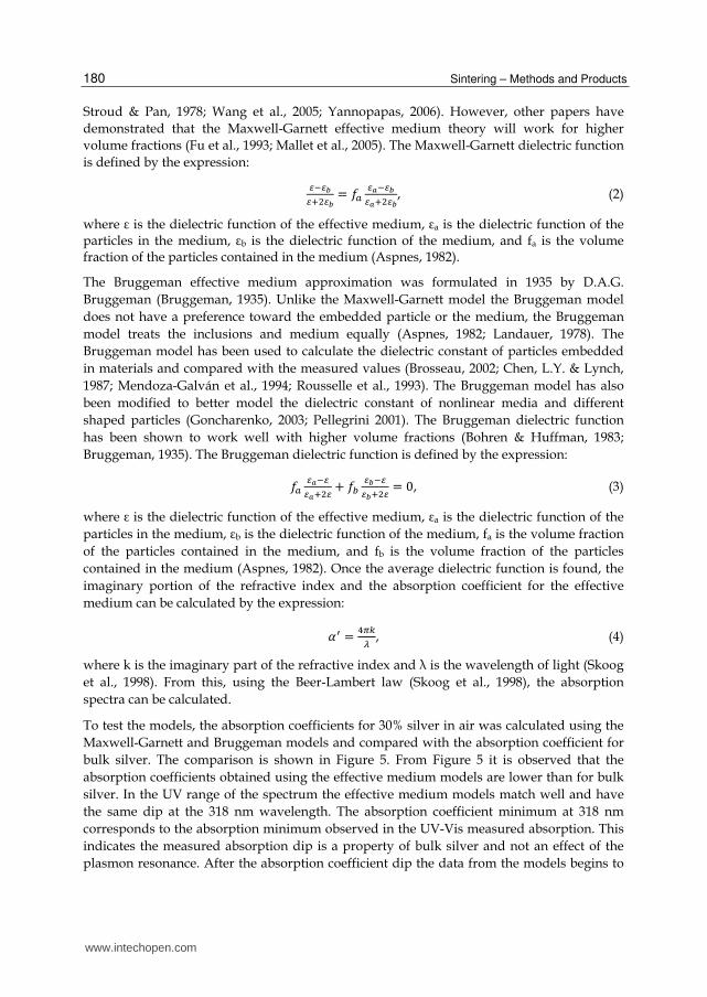
To test the models, the absorption coefficients for 30% silver in air was calculated using the
Maxwell-Garnett and Bruggeman models and compared with the absorption coefficient for
bulk silver. The comparison is shown in Figure 5. From Figure 5 it is observed that the
absorption coefficients obtained using the effective medium models are lower than for bulk
silver. In the UV range of the spectrum the effective medium models match well and have
the same dip at the 318 nm wavelength. The absorption coefficient minimum at 318 nm
corresponds to the absorption minimum observed in the UV-Vis measured absorption. This
indicates the measured absorption dip is a property of bulk silver and not an effect of the
plasmon resonance. After the absorption coefficient dip the data from the models begins to
www.intechopen.com
Photonic Sintering of Silver Nanoparticles: Comparison of Experiment and Theory 181
diverge. The absorption coefficient from the Maxwell-Garnett model rises sharply, becomes
higher than for bulk silver, and peaks at the 380 nm wavelength mark. This peak in the
absorption coefficient is near the surface plasmon resonance that has been seen in the
literature for silver nanoparticles dispersed in an aqueous solution (Chen, T.C. et al., 2004;
Hutter et al., 2001; Lim et al., 2005). The Maxwell-Garnett data then drops rapidly to near
zero for the remainder of the modeled wavelength area. After the 318 nm wavelength mark
the Bruggeman data gently rises for the remainder of the wavelengths modeled. Thus the
Bruggeman model will most closely matches the measured data in our experiments.
Fig. 5. Comparison of the absorption coefficients for 30% silver in air using Maxwell-Garnett and Bruggeman effective medium models with the values for bulk silver.
To obtain a closer look at how the Bruggeman absorption curve and the measured
absorption curve compare, the thickness of the deposition for the Bruggeman model was set
to 160 nm and is shown in Figure 6 compared with the 1.3 ┤m thick measured absorption.
The absorption minimums in Figure 6 are 62% for the Bruggeman model at 316 nm and 64%
at 322 nm for the measured silver. In the UV and near IR regimes the absorption curves have
a similar slope. After the absorption minimum the Bruggeman model absorption is
relatively constant through the visible spectrum while the measured data rises constantly
before leveling off. Though the absorption as modeled using the Bruggeman effective
medium theory is stronger than what was measured, unlike the Maxwell-Garnett model, the
Bruggeman model closely follows the measured absorption dip and does not decrease
significantly at longer wavelengths. The discrepancy in the theoretical and experimental
thicknesses would suggest that most of the absorption takes place near the surface of the
film. However, the spectral characteristics of the Bruggeman model reproduce very well the
experimental data, and thus were was used to model the absorption of the deposited
materials in this work.
0.000
1.000
2.000
3.000
4.000
5.000
6.000
200 400 600 800
k
wavelength (nm)
Silver k
MaxwellGarnett kBruggeman k
www.intechopen.com

Sintering – Methods and Products 182
Fig. 6. Absorption vs. wavelength for 30% volume fraction silver, 160 nm thick film using
Bruggeman model and a 1.3 ┤m thick measured silver film.
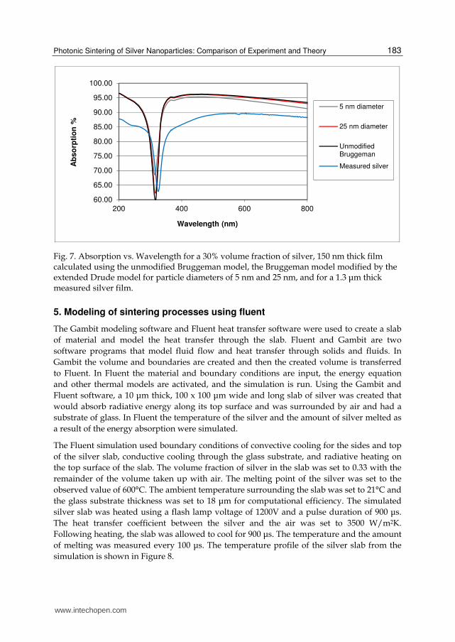
4.1 Modifying the bruggeman model with the extended drude model
As the calculated absorption using the Bruggeman model does not perfectly match the
measured absorption, the complex dielectric function was modified using the extended
Drude model in an attempt to bring the calculated and measured absorption closer together
(Haiss et al., 2007; Kreibig & Vonfrags, 1969). The extended Drude model was used to
modify the dielectric function of silver for particle diameters of 25 nm and 5 nm. The
absorption was then calculated using a volume fraction of 30% and a film thickness of 150
nm and compared with the measured absorption and the unmodified Bruggeman model.
This is shown in Figure 7. The thickness of the film was thinned to 150 nm to bring the
modified Bruggeman model with the 25 nm diameter silver particles in line with the
measured silver absorption. Figure 7 shows that in the UV portion of the spectrum the
particle size did not affect the absorption of the silver film. The particle size did affect the
absorption minimum slightly with the minimum occurring at 314 nm for the 5 nm diameter
silver with a minimum absorption of 68.5%. The 5 nm diameter silver also had a calculated
absorption in the visible range slightly below the unmodified Bruggeman and Drude
modified Bruggeman absorptions. The 25 nm diameter calculated absorption using the
extended Drude and Bruggeman models agreed well with the unmodified Bruggeman
calculated absorption in the UV and visible ranges. The main difference was that the
absorption minimum at 316 nm was 3.5% stronger for the Drude modified Bruggeman
model than for the unmodified Bruggeman absorption. These comparisons indicate that the
particle size does not play a large role in the absorption by nanoparticle films with volume
fractions of 30% or greater. The nanoparticle silver films appear to act more like bulk silver
than like individual silver nanoparticles. This is shown through a surface plasmon
resonance peak not appearing in the measured absorptions. The reason for the absorption
appearing to be so strong in the calculated absorptions as opposed to the measured data
could be due to the majority of the absorption occurring within the first few hundred
nanometers of the films, with the absorption only slightly increasing beyond that depth.
50.00
60.00
70.00
80.00
90.00
100.00
200 300 400 500 600 700 800
Ab
sorp
tio
n %
Wavelength (nm)
Measured Silver Bruggeman
www.intechopen.com
Photonic Sintering of Silver Nanoparticles: Comparison of Experiment and Theory 183
Fig. 7. Absorption vs. Wavelength for a 30% volume fraction of silver, 150 nm thick film calculated using the unmodified Bruggeman model, the Bruggeman model modified by the extended Drude model for particle diameters of 5 nm and 25 nm, and for a 1.3 ┤m thick measured silver film.
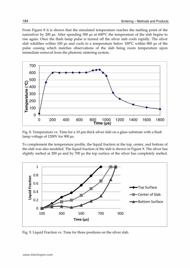
5. Modeling of sintering processes using fluent
The Gambit modeling software and Fluent heat transfer software were used to create a slab
of material and model the heat transfer through the slab. Fluent and Gambit are two
software programs that model fluid flow and heat transfer through solids and fluids. In
Gambit the volume and boundaries are created and then the created volume is transferred
to Fluent. In Fluent the material and boundary conditions are input, the energy equation
and other thermal models are activated, and the simulation is run. Using the Gambit and
Fluent software, a 10 ┤m thick, 100 x 100 ┤m wide and long slab of silver was created that
would absorb radiative energy along its top surface and was surrounded by air and had a
substrate of glass. In Fluent the temperature of the silver and the amount of silver melted as
a result of the energy absorption were simulated.
The Fluent simulation used boundary conditions of convective cooling for the sides and top
of the silver slab, conductive cooling through the glass substrate, and radiative heating on
the top surface of the slab. The volume fraction of silver in the slab was set to 0.33 with the
remainder of the volume taken up with air. The melting point of the silver was set to the
observed value of 600°C. The ambient temperature surrounding the slab was set to 21°C and
the glass substrate thickness was set to 18 ┤m for computational efficiency. The simulated
silver slab was heated using a flash lamp voltage of 1200V and a pulse duration of 900 ┤s.
The heat transfer coefficient between the silver and the air was set to 3500 W/m2K.
Following heating, the slab was allowed to cool for 900 ┤s. The temperature and the amount
of melting was measured every 100 ┤s. The temperature profile of the silver slab from the
simulation is shown in Figure 8.
60.00
65.00
70.00
75.00
80.00
85.00
90.00
95.00
100.00
200 400 600 800
Ab
so
rpti
on
%
Wavelength (nm)
5 nm diameter
25 nm diameter
UnmodifiedBruggeman
Measured silver
www.intechopen.com
Sintering – Methods and Products 184
From Figure 8 it is shown that the simulated temperature reaches the melting point of the
nanosilver by 200 ┤s. After spending 500 ┤s at 600°C the temperature of the slab begins to
rise again. Once the flash lamp pulse is turned off the silver slab cools rapidly. The silver
slab solidifies within 100 ┤s and cools to a temperature below 100°C within 800 ┤s of the
pulse ceasing which matches observations of the slab being room temperature upon
immediate removal from the photonic sintering system.
Fig. 8. Temperature vs. Time for a 10 ┤m thick silver slab on a glass substrate with a flash lamp voltage of 1200V for 900 ┤s.
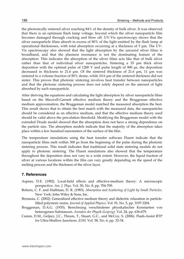
To complement the temperature profile, the liquid fraction at the top, center, and bottom of
the slab was also modeled. The liquid fraction of the slab is shown in Figure 9. The silver has
slightly melted at 200 ┤s and by 700 ┤s the top surface of the silver has completely melted.
Fig. 9. Liquid Fraction vs. Time for three positions on the silver slab.
0
100
200
300
400
500
600
700
0 200 400 600 800 1000 1200 1400 1600 1800
Te
mp
era
ture
(°C
)
Time (μs)
0
0.2
0.4
0.6
0.8
1
100 300 500 700 900
Liq
uid
Fra
ctio
n
Time (μs)
Top Surface
Center of Slab
Bottom Surface
www.intechopen.com

Photonic Sintering of Silver Nanoparticles: Comparison of Experiment and Theory 185
The bottom surface of the silver takes until 850 ┤s to completely melt. After the top surface of the silver has completely melted the temperature begins to rise again as seen in Figure 8. This matches the premise based on the densification measurements and simulation data that at 300 ┤s the silver has just begun to melt, the melting is still in progress at 600 ┤s, and the material has completely melted by 900 ┤s. This gives a relatively slow melting time allowing the material to sinter at a rate that will not crack or ablate the material off the substrate.
After simulating the temperature of the 10 ┤m thick silver slab on glass the silver slab was
thinned to 3 ┤m, as 3 ┤m is the typical deposition thickness. For the thinner slab some
conditions were modified to make them more accurate. The porosity of the silver slab
remained at 33%. The heat transfer coefficient was set to 3100 W/m2K as the simulations on
glass showed the silver remaining near 600°C. The emissivity was set to 0.99 to allow the
appropriate amount of the pulse to pass through the deposition. The melting temperature
remained at 600°C and the ambient temperature was set to 21°C. The flash lamp voltage was
set to 1200V and the pulse was set to a length of 900 ┤s, after which 900 ┤s of cooling was
simulated. The thickness of the glass substrate was increased to 20 ┤m. The resultant graph
of temperature versus time is shown in Figure 10. From observing the liquid fraction the
simulation indicates that for the thinner slab the deposition has melted 93% after the pulse
has been active for 100 ┤s. The temperature reaches 701°C by 200 ┤s and then decreases to
644°C at 300 ┤s and proceeds to increase at a constant rate for the duration of the pulse.
Once the pulse ends the temperature rapidly decreases. One difference from using the 3 ┤m
slab instead of the 10 ┤m slab is the early peak of slab temperature at 200 ┤s. Another
difference is that the thinner slab melts quicker, which is expected as the thin slab is
absorbing nearly the same amount of energy and has less mass to heat.
Fig. 10. Temperature vs. time for a 3 ┤m thick silver slab using a 1200V flash lamp voltage
and a 900 ┤s pulse length using Fluent.
6. Conclusions
In examining the photonic sintering process a number of interesting results were found. It was shown that there is significant densification of the photonically sintered silver, with
0
100
200
300
400
500
600
700
800
0 300 600 900 1200 1500 1800
Te
mp
era
ture
(°C
)
Time (μs)
www.intechopen.com
Sintering – Methods and Products 186
the photonically sintered silver reaching 84% of the density of bulk silver. It was observed that there is an optimum flash lamp voltage, beyond which the silver nanoparticle film becomes damaged through cracking and blow off. UV-Vis spectroscopy shows that the silver nanoparticle films absorb in excess of 80% of the light emitted by the flash lamp at operational thicknesses, with total absorption occurring at a thickness of 5 ┤m. The UV-Vis spectroscopy also showed that the light absorption by the uncured silver films is broadband, and that the plasmon resonance is not the dominating feature of the absorption. This indicates the absorption of the silver films acts like that of bulk silver rather than that of individual silver nanoparticles. Sintering a 35 ┤m thick silver deposition with the optimal pulse of 1200 V and pulse length of 900 ┤s, the deposition decreased in thickness to 21.6 ┤m. Of the sintered thickness of 21.6 ┤m, 11 ┤m was sintered to a volume fraction of 80% dense, while 10.6 ┤m of the sintered thickness did not sinter. This proves that photonic sintering involves heat transfer between nanoparticles and that the photonic sintering process does not solely depend on the amount of light absorbed by each nanoparticle.
After deriving the equations and calculating the light absorption by silver nanoparticle films
based on the Maxwell-Garnett effective medium theory and the Bruggeman effective
medium approximation, the Bruggeman model matched the measured absorption the best.
This result shows that to obtain the best match with the measured data, the nanoparticles
should be considered as an effective medium, and that the effective medium theory used
should be valid above the percolation threshold. Modifying the Bruggeman model with the
extended Drude model showed that the absorption does not have a strong dependence on
the particle size. The absorption models indicate that the majority of the absorption takes
place within a few hundred nanometers of the surface of the film.
The temperature simulations using the heat transfer software Fluent indicate that the
nanoparticle films melt within 300 ┤s from the beginning of the pulse during the photonic
sintering process. This result indicates that traditional solid state sintering models do not
apply to photonic sintering. The Fluent simulations also showed that the temperature
throughout the deposition does not vary to a wide extent. However, the liquid fraction of
silver at various locations within the film can vary greatly depending on the speed of the
melting process and the thickness of the silver layer.
7. References
Aspnes, D.E. (1982). Local-field effects and effective-medium theory: A microscopic
perspective. Am. J. Phys. Vol. 50, No. 8, pp. 704-709.
Bohren, C. F. and Huffman, D. R. (1983). Absorption and Scattering of Light by Small Particles.
New York: John Wiley & Sons, Inc.
Brosseau, C. (2002). Generalized effective medium theory and dielectric relaxation in particle-
filled polymeric resins. Journal of Applied Physics. Vol. 91, No. 5, pp. 3197-3204.
Bruggeman, D.A.G. (1935). Berechnung verschiedener physikalischer Konstanten von
heterogenen Substanzen. Annalen der Physik (Leipzig). Vol. 24, pp. 636-679.
Camm, D.M., Gelpey, J.C., Thrum, T., Stuart, G.C., and McCoy, S. (2006). Flash-Assist RTP
for Ultra-Shallow Junctions. JOM, Vol. 58, No. 6, pp. 32-34.
www.intechopen.com
Photonic Sintering of Silver Nanoparticles: Comparison of Experiment and Theory 187
Carter, M. and Sears, J. (2007). Photonic Curing for Sintering of Nano-Particulate Material. Advances in Powder Metallurgy & Particulate Materials – 2007: Proceedings of the 2007 International Conference on Powder Metallurgy & Particulate Materials, May 13-16, Denver, Colorado.
Chen, L.Y., Lynch, D.W. (1987). Effect of liquids on the Drude dielectric function of Ag and
Au films. Physical Review B. Vol. 36, No. 3, pp. 1425-1431.
Chen, T.C., Su, W.K., and Lin, Y.L. (2004). A Surface Plasmon Resonance Study of Ag
Nanoparticles in an Aqueous Solution. Japanese Journal of Applied Physics, Vol. 43,
pp. L119-L122.
Chen, T.C., Su, W.K., and Lin, Y.L. (2004). A Surface Plasmon Resonance Study of Ag
Nanoparticles in an Aqueous Solution. Japanese Journal of Applied Physics. Vol. 43,
pp. L119-L122.
Claro, F., Rojas, R. (1991). Correlation and multipolar effects in the dielectric response of
particulate matter: An iterative mean-field theory. Physical Review B. Vol. 42, No. 8,
pp. 6369-6375.
Datta, S., Chan, C.T., Ho, K.M., Soukoulis, C.M. (1993). Effective dielectric constant of
periodic composite structures. Physical Review B. Vol. 48, No. 20, pp. 14936-14943.
Davis, V.A., Schwartz, L. (1985). Electromagnetic propagation in close-packed disordered
suspensions. Physical Review B. Vol. 31, No. 8, pp. 5155-5165.
Farnsworth, Stan. Curing Copper and other Thin-Film Materials at Production Speeds.
SEMICON West. Moscone Center, San Francisco. 16 July 2009.
Fu, L., Macedo, P.B., Resca, L. (1993). Analytic approach to the interfacial polarization of
heterogeneous systems. Physical Review B. Vol. 47, No. 20, pp. 13818-13829.
Gibson, U.J. and Buhrman, R.A. (1983). Optical response of Cermet composite films in the
microstructural transition region. Physical Review B. Vol. 27, No. 8, pp. 5046-5051.
Goncharenko, A.V. (2003). Generalizations of the Bruggeman equation and a concept of
shape-distributed particle composites. Physical Review E. Vol. 68, 041108.
Grechko, L.G., Whites, K.W., Pustovit, V.N., Lysenko, V.S. (2000). Macroscopic dielectric
response of the metallic particles embedded in host dielectric medium.
Microelectronics Reliability. Vol. 40, pp. 893-895.
Haiss, W., Thanh, N., Aveyard, J., and Fernig, D. (2007). Determination of Size and
Concentration of Gold Nanoparticles from UV-Vis Spectra. Analytical Chemistry.
Vol. 79, pp. 4215-4221.
Hutter, E., Fendler, J.H., and Roy, D. (2001). Surface Plasmon Resonance Studies of Gold and
Silver Nanoparticles Linked to Gold and Silver Substrates by 2-Aminoethanethiol
and 1,6-Hexanedithiol. J. Phys. Chem. B., Vol. 105, pp. 11159-11168.
Hutter, E., Fendler, J.H., and Roy, D. (2001). Surface Plasmon Resonance Studies of Gold and
Silver Nanoparticles Linked to Gold and Silver Substrates by 2-Aminoethanethiol
and 1,6-Hexanedithiol. J. Phys. Chem. B. Vol 105, pp. 11159-11168.
Kim, H.S., Dhage, S.R., Shim, D.E., and Hahn, H.T. (2009). Intense pulse light sintering of
copper nanoink for printed electronics. Applied Physics A, Vol. 97, pp. 791-798.
Kreibig, U. and Vonfrags. C. (1969). The Limitation of Electron Mean Free Path in Small
Silver Particles. Z. Physik. Vol. 224, pp. 307-323.
Lamb, W., Wood, D.M., Ashcroft, N.W. (1980). Long-wavelength electromagnetic
propagation in heterogeneous media. Physical Review B. Vol. 21, No. 6, pp. 2248-
2266.
www.intechopen.com
Sintering – Methods and Products 188
Landauer, R. (1978). Electrical conductivity in inhomogeneous media. AIP Conference
Proceedings. Vol. 40, No. 1, pp. 2-45.
Li, J., Sun, G., Chan, C.T. (2006). Optical properties of photonic crystals composed of metal-
coated spheres. Physical Review B. Vol. 73, 075117.
Lidorikis, E., Egusa, S., Joannopoulos, J.D. (2007). Effective medium properties and photonic
crystal superstructures of metallic nanoparticle arrays. Journal of Applied Physics.
Vol. 101, 054304.
Lim, S.K., Chung, K.J., Kim, C.K., Shin, D.W., Kim, Y.H., and Yoon, C.S. (2005). Surface-
plasmon resonance of Ag nanoparticles in polyimide. Journal of Applied Physics, Vol.
98, No. 8, 084309.
Lim, S.K., Chung, K.J., Kim, C.K., Shin, D.W., Kim, Y.H., and Yoon, C.S. (2005). Surface-
plasmon resonance of Ag nanoparticles in polyimide. Journal of Applied Physics. Vol.
98, No. 8, 084309.
Mallet, P., Guérin, C.A., Sentenac, A. (2005). Maxwell-Garnett mixing rule in the presence of
multiple scattering: Derivation and accuracy. Physical Review B. Vol. 72, 014205.
Maxwell Garnett, J. C. (1904). Colors in metal glasses and in metallic films. Philos. Trans. R.
Soc., Vol. A203, pp. 385-420.
Mendoza-Galván, A., Martínez, G., Martínez, J.L. (1994). Effective dielectric function
modeling of inhomogeneous and anisotropic silver films. Physica A. Vol. 207, pp.
365-371.
Novacentrix. (2007). PCS-1100 Photonic Curing System Operations and Safety Manual. Austin:
Novacentrix Corp.
Novacentrix. (2009). PulseForge 3100 Development and Production: Metals Processing. Available
from <http://www.novacentrix.com/product/pf3100.php>.
Novacentrix. (2009). PulseForge 3300 Development and Production: Semiconductor and
Photovoltaic Materials Processing. Available from <http://www.novacentrix.com
/product/pf3300.php>.
Pellegrini, Y.P. (2001). Self-consistent effective-medium approximation for strongly
nonlinear media. Physical Review B. Vol. 64, 134211.
Rousselle, D., Berthault, A., Acher, O., Bouchaud, J.P., Zérah, P.G. (1993). Effective medium
at finite frequency: Theory and experiment. Journal of Applied Physics. Vol. 74, No. 1,
pp. 475-479.
Schroder, K.A., McCool, S.C., and Furlan, W.R. (2006). Broadcast Photonic Curing of
Metallic Nanoparticle Films. Technical Proceedings of the 2006 NSTI Nanotechnology
Conference and Trade Show, Volume 3, pp. 198-201.
Skoog, D., Holler, F. J., Nieman, T. (1998). Principles of Instrumental Analysis. Thompson
Learning.
Stroud, D., Pan, F.P. (1978). Self-consistent approach to electromagnetic wave propagation in
composite media: Application to model granular metals. Physical Review B. Vol. 17,
No. 4, pp. 1602-1610.
Wang, J., Lau, W.M., Li, Q. (2005). Effects of particle size and spacing on the optical
properties of gold nanocrystals in alumina. Journal of Applied Physics. Vol. 97,
114303.
Yannopapas, V. (2006). Effective-medium description of disordered photonic alloys. J. Opt.
Soc. Am. B. Vol. 23, No. 7, pp. 1414-1419.
www.intechopen.com

Sintering - Methods and ProductsEdited by Dr. Volodymyr Shatokha
ISBN 978-953-51-0371-4Hard cover, 316 pagesPublisher InTechPublished online 23, March, 2012Published in print edition March, 2012
InTech EuropeUniversity Campus STeP Ri Slavka Krautzeka 83/A 51000 Rijeka, Croatia Phone: +385 (51) 770 447 Fax: +385 (51) 686 166www.intechopen.com
InTech ChinaUnit 405, Office Block, Hotel Equatorial Shanghai No.65, Yan An Road (West), Shanghai, 200040, China
Phone: +86-21-62489820 Fax: +86-21-62489821
This book is addressed to a large and multidisciplinary audience of researchers and students dealing with orinterested in sintering. Though commonly known as a method for production of objects from fines or powders,sintering is a very complex physicochemical phenomenon. It is complex because it involves a number ofphenomena exhibiting themselves in various heterogeneous material systems, in a wide temperature range,and in different physical states. It is multidisciplinary research area because understanding of sinteringrequires a broad knowledge - from solid state physics and fluid dynamics to thermodynamics and kinetics ofchemical reactions. Finally, sintering is not only a phenomenon. As a material processing method, sinteringembraces the wide group of technologies used to obtain such different products as for example iron oreagglomerate and luminescent powders. As a matter of fact, this publication is a rare opportunity to connect theresearchers involved in different domains of sintering in a single book.
How to referenceIn order to correctly reference this scholarly work, feel free to copy and paste the following:
Jeff West, Michael Carter, Steve Smith and James Sears (2012). Photonic Sintering of Silver Nanoparticles:Comparison of Experiment and Theory, Sintering - Methods and Products, Dr. Volodymyr Shatokha (Ed.),ISBN: 978-953-51-0371-4, InTech, Available from: http://www.intechopen.com/books/sintering-methods-and-products/photonic-sintering-of-silver-nanoparticles-comparison-of-experiment-and-theory

© 2012 The Author(s). Licensee IntechOpen. This is an open access articledistributed under the terms of the Creative Commons Attribution 3.0License, which permits unrestricted use, distribution, and reproduction inany medium, provided the original work is properly cited.