Photonic devices · Photonic devices Photonic devices can be devided into three groups: 1. devices...
12
Photonic devices Photonic devices Photonic devices can be devided into three groups: 1. devices that convert electrical energy into optical radiation (spontaneous emission): LED (light emitting diodes), LASER (light amplification by stimulated emission of radiation). 2. devices that detect optical signals through electronic processes (photodetectors). 3. devices that convert optical radiation into electrical energy (photovoltaic device or solar cell). History 1954 Townes and al. invented the Maser (microwave amplification by stimulated emission of radiation) and the subsequent operation of optical maser and laser (light), semiconductors were suggested for use as laser materials. 1961 Theoretical calculations by Bernard and Duraffourg 1962 Dumke showed that laser action was indeed possible in direct bandgap semiconductor 1962 Three groups announced simultaneously that they had achieved lasing in semiconductors (pulsed at LN, forward-biased GaAs p-n junction). 1970 RT operation by use of heterostructure LASER Text: S.M. Sze, Physics of Semiconductor Devices, J. Wiley &Sons, 1981 J. Singh, Semiconductor devices, Mc-Graw-Holl Intern. Editions 1
Transcript of Photonic devices · Photonic devices Photonic devices can be devided into three groups: 1. devices...

Photonic devicesPhotonic devices
Photonic devices can be devided into three groups:1. devices that convert electrical energy into optical radiation (spontaneous
emission): LED (light emitting diodes), LASER (light amplification by stimulatedemission of radiation).
2. devices that detect optical signals through electronic processes (photodetectors).3. devices that convert optical radiation into electrical energy (photovoltaic device or
solar cell).History1954 Townes and al. invented the Maser (microwave amplification by stimulated
emission of radiation) and the subsequent operation of optical maser and laser(light), semiconductors were suggested for use as laser materials.
1961 Theoretical calculations by Bernard and Duraffourg1962 Dumke showed that laser action was indeed possible in direct bandgap
semiconductor1962 Three groups announced simultaneously that they had achieved lasing in
semiconductors (pulsed at LN, forward-biased GaAs p-n junction).1970 RT operation by use of heterostructure LASERText: S.M. Sze, Physics of Semiconductor Devices, J. Wiley &Sons, 1981J. Singh, Semiconductor devices, Mc-Graw-Holl Intern. Editions
1
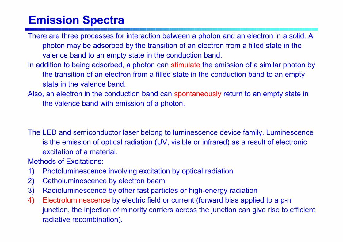
Emission SpectraEmission SpectraThere are three processes for interaction between a photon and an electron in a solid. A
photon may be adsorbed by the transition of an electron from a filled state in thevalence band to an empty state in the conduction band.
In addition to being adsorbed, a photon can stimulate the emission of a similar photon bythe transition of an electron from a filled state in the conduction band to an emptystate in the valence band.
Also, an electron in the conduction band can spontaneously return to an empty state inthe valence band with emission of a photon.
The LED and semiconductor laser belong to luminescence device family. Luminescenceis the emission of optical radiation (UV, visible or infrared) as a result of electronicexcitation of a material.
Methods of Excitations:1) Photoluminescence involving excitation by optical radiation2) Catholuminescence by electron beam3) Radioluminescence by other fast particles or high-energy radiation4) Electroluminescence by electric field or current (forward bias applied to a p-n
junction, the injection of minority carriers across the junction can give rise to efficientradiative recombination).

p-np-n Junction Junction
In the forward bias conditions the electrons (holes) are injected from the n-side (p-side)to the p-side (n-side) and they may recombine to produce photons.
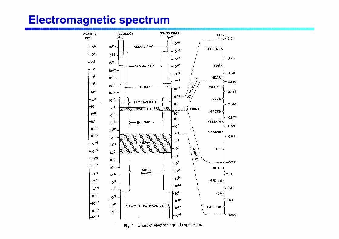
Electromagnetic spectrumElectromagnetic spectrum
Light-Light-emitting Diodesemitting Diodes
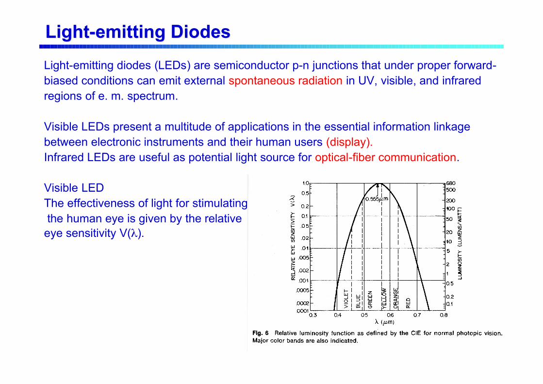
Light-emitting diodes (LEDs) are semiconductor p-n junctions that under proper forward-biased conditions can emit external spontaneous radiation in UV, visible, and infraredregions of e. m. spectrum.
Visible LEDs present a multitude of applications in the essential information linkagebetween electronic instruments and their human users (display).Infrared LEDs are useful as potential light source for optical-fiber communication.
Visible LEDThe effectiveness of light for stimulating the human eye is given by the relativeeye sensitivity V(λ).
Materials for visibleMaterials for visible LED LED
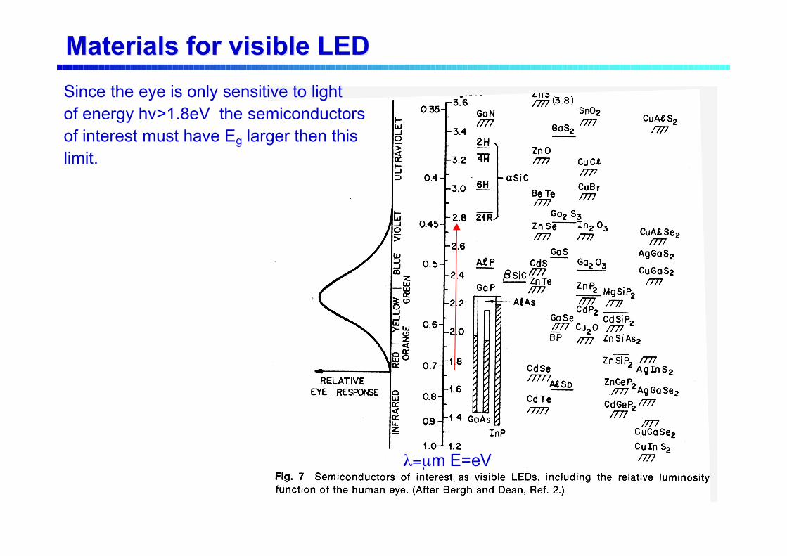
Since the eye is only sensitive to lightof energy hv>1.8eV the semiconductorsof interest must have Eg larger then thislimit.
λ=µm E=eV
Loss CharacteristicsLoss Characteristics
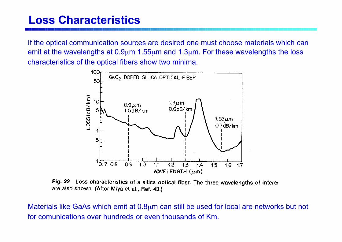
If the optical communication sources are desired one must choose materials which canemit at the wavelengths at 0.9µm 1.55µm and 1.3µm. For these wavelengths the losscharacteristics of the optical fibers show two minima.
Materials like GaAs which emit at 0.8µm can still be used for local are networks but notfor comunications over hundreds or even thousands of Km.

Radiative EfficiencyRadiative Efficiency: direct: direct vs indirect vs indirect band-gap band-gap
Red x=0.4 orange (direct bandgap) x=0.65,yellow x=0.85, green x=1 (indirect bandgap)
GaAs1-xPx
The momentum conservation causes strong radiative transitions to occur only in directgap semiconductors. Some indirect gap materials can, have a reasonable radiative (LEDbut not LASER) efficiency if they are doped withcertain impurities.
LED LED SubstratesSubstrates
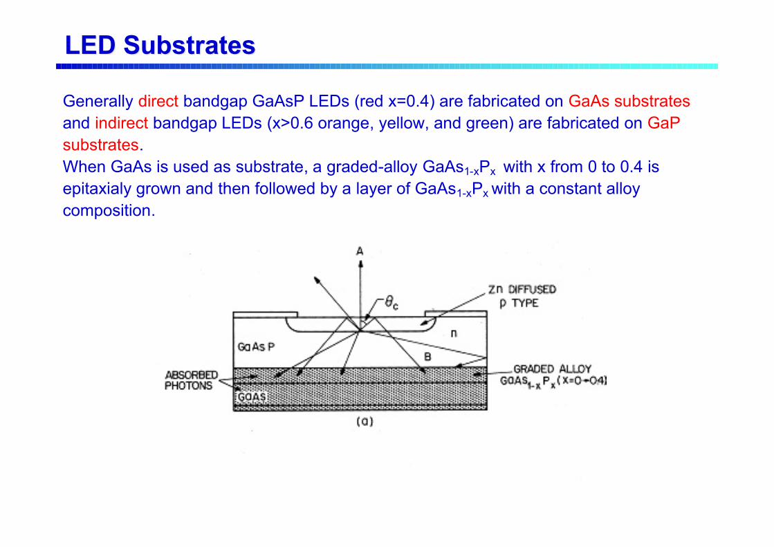
Generally direct bandgap GaAsP LEDs (red x=0.4) are fabricated on GaAs substratesand indirect bandgap LEDs (x>0.6 orange, yellow, and green) are fabricated on GaPsubstrates.When GaAs is used as substrate, a graded-alloy GaAs1-xPx with x from 0 to 0.4 isepitaxialy grown and then followed by a layer of GaAs1-xPx with a constant alloycomposition.

Loss MechanismsLoss Mechanisms
The photons generated at the junction are emitted in all directions, but only a fraction ofthese photons can emerge from the surface to reach the eye of an observer(losses).
There are three main loss mechanisms dot the emitted photons:1) They can be readsorbed in the semiconductor by creating an electron-hole pair;2) a certain fraction of photons will be reflected back at the semiconductor-air interface3) Some photons impinge upon the surface with angles greater than the critical angle
ths suffering total internal reflection.
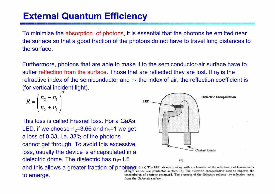
ExternalExternal Quantum Quantum Efficiency Efficiency
To minimize the absorption of photons, it is essential that the photons be emitted nearthe surface so that a good fraction of the photons do not have to travel long distances tothe surface.
Furthermore, photons that are able to make it to the semiconductor-air surface have tosuffer reflection from the surface. Those that are reflected they are lost. If n2 is therefractive index of the semiconductor and n1 the index of air, the reflection coefficient is(for vertical incident light),
2
12
12
+
−=
nn
nnR
This loss is called Fresnel loss. For a GaAsLED, if we choose n2=3.66 and n1=1 we geta loss of 0.33, i.e. 33% of the photonscannot get through. To avoid this excessiveloss, usually the device is encapsulated in adielectric dome. The dielectric has n1≈1.6and this allows a greater fraction of photonsto emerge.
ExternalExternal Quantum Quantum Efficiency Efficiency
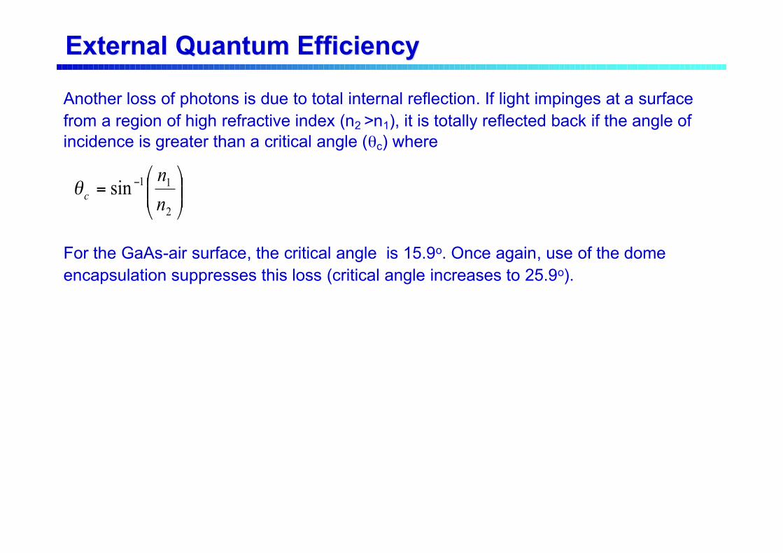
Another loss of photons is due to total internal reflection. If light impinges at a surfacefrom a region of high refractive index (n2 >n1), it is totally reflected back if the angle ofincidence is greater than a critical angle (θc) where
For the GaAs-air surface, the critical angle is 15.9o. Once again, use of the domeencapsulation suppresses this loss (critical angle increases to 25.9o).
= −
2
11sinn
ncθ