
Photolithography - users.wfu.edu · Wafer Cleaning - 1 • Typical contaminants that must be...
33
Photolithography Source: Dr. R. B. Darling (UW) lecture notes on photolithography
Transcript of Photolithography - users.wfu.edu · Wafer Cleaning - 1 • Typical contaminants that must be...

Photolithography
Source: Dr. R. B. Darling (UW) lecture notes on photolithography
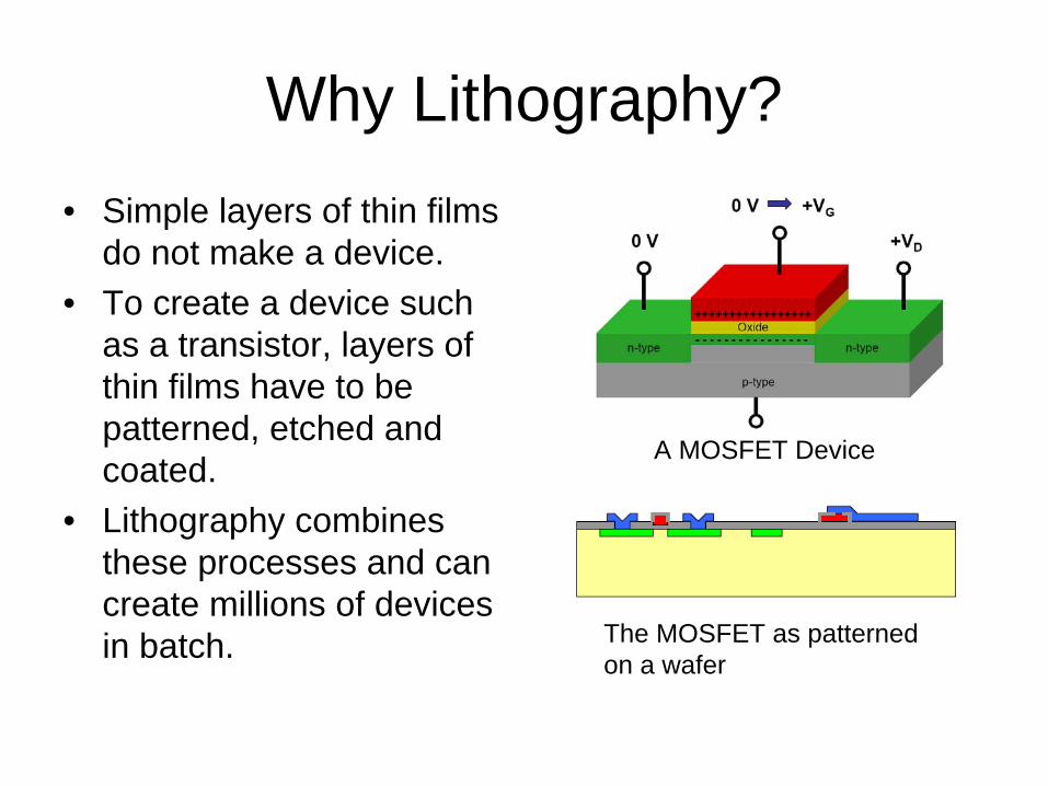
Why Lithography?• Simple layers of thin films
do not make a device.• To create a device such
as a transistor, layers of thin films have to be patterned, etched and coated.
• Lithography combines these processes and can create millions of devices in batch.
A MOSFET Device
The MOSFET as patterned on a wafer
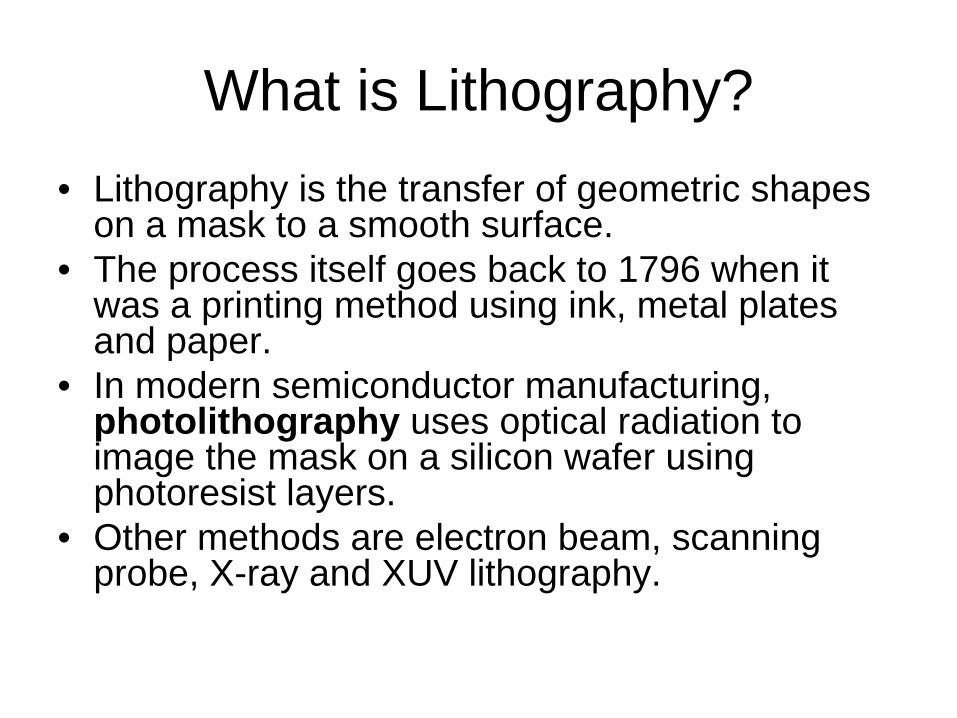
What is Lithography?• Lithography is the transfer of geometric shapes
on a mask to a smooth surface.• The process itself goes back to 1796 when it
was a printing method using ink, metal plates and paper.
• In modern semiconductor manufacturing, photolithography uses optical radiation to image the mask on a silicon wafer using photoresist layers.
• Other methods are electron beam, scanning probe, X-ray and XUV lithography.
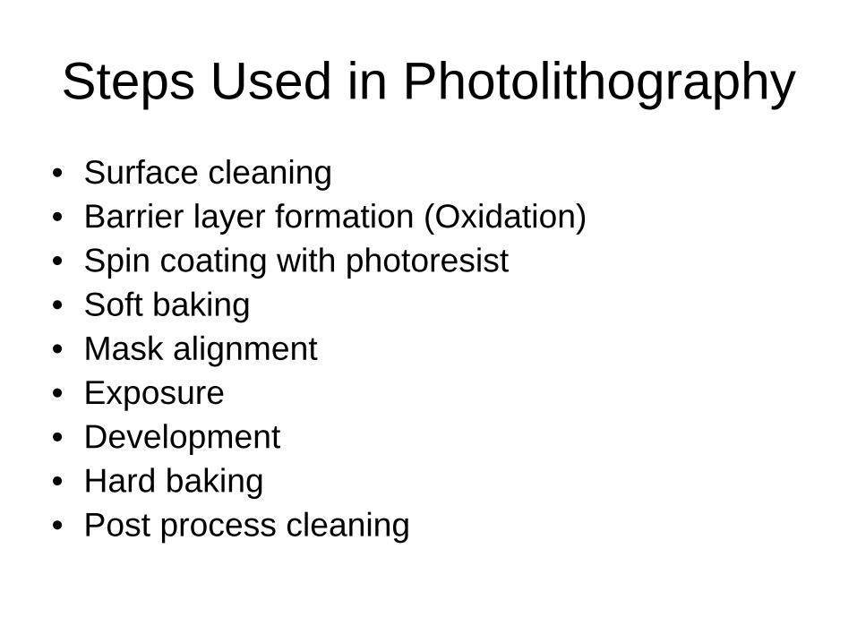
Steps Used in Photolithography• Surface cleaning• Barrier layer formation (Oxidation)• Spin coating with photoresist• Soft baking• Mask alignment• Exposure• Development• Hard baking• Post process cleaning
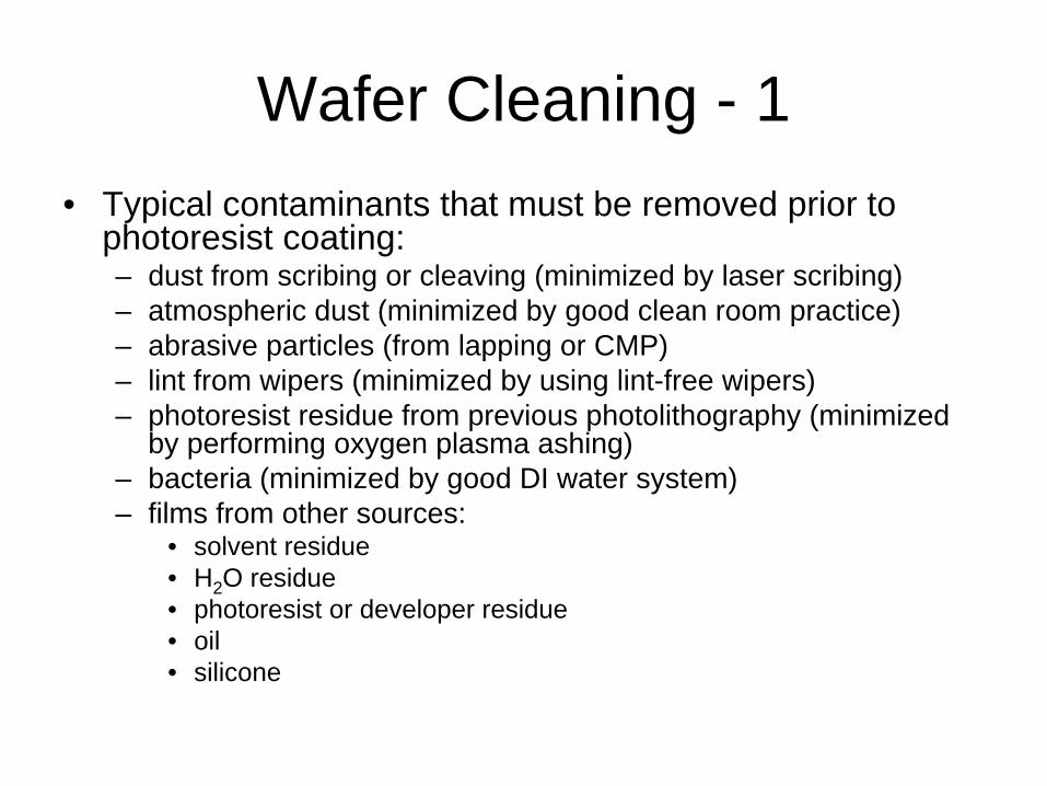
Wafer Cleaning - 1• Typical contaminants that must be removed prior to
photoresist coating:– dust from scribing or cleaving (minimized by laser scribing)– atmospheric dust (minimized by good clean room practice)– abrasive particles (from lapping or CMP)– lint from wipers (minimized by using lint-free wipers)– photoresist residue from previous photolithography (minimized
by performing oxygen plasma ashing)– bacteria (minimized by good DI water system)– films from other sources:
• solvent residue• H2 O residue• photoresist or developer residue• oil• silicone
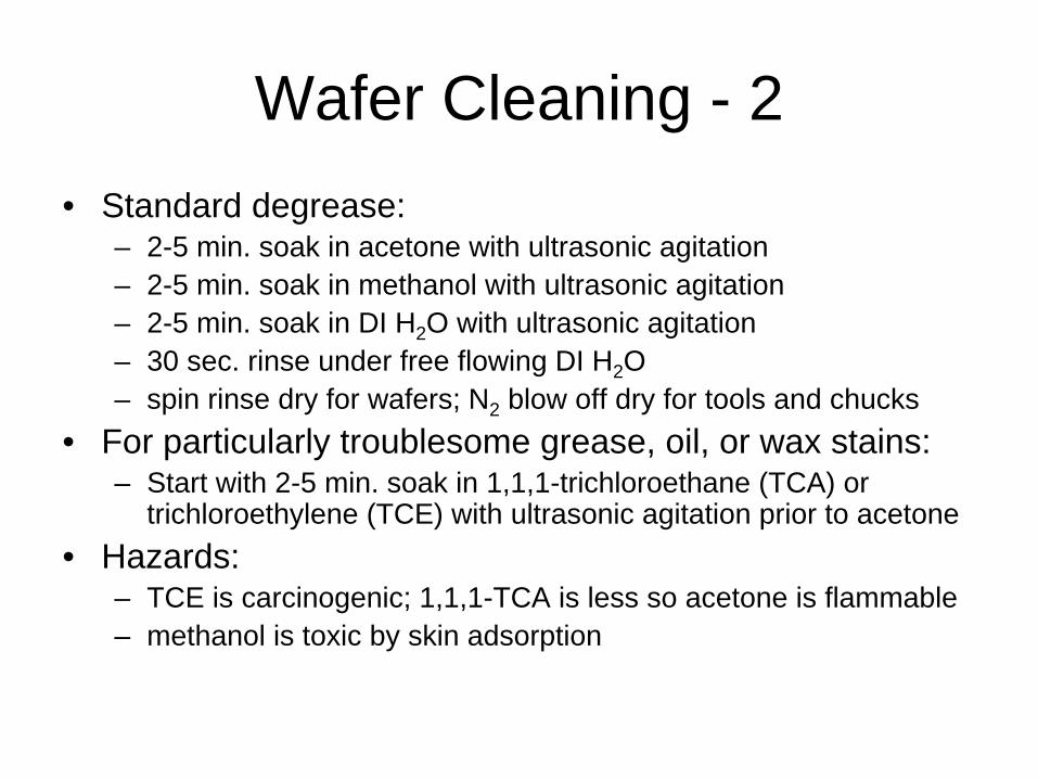
Wafer Cleaning - 2• Standard degrease:
– 2-5 min. soak in acetone with ultrasonic agitation– 2-5 min. soak in methanol with ultrasonic agitation– 2-5 min. soak in DI H2 O with ultrasonic agitation– 30 sec. rinse under free flowing DI H2 O– spin rinse dry for wafers; N2 blow off dry for tools and chucks
• For particularly troublesome grease, oil, or wax stains:– Start with 2-5 min. soak in 1,1,1-trichloroethane (TCA) or
trichloroethylene (TCE) with ultrasonic agitation prior to acetone• Hazards:
– TCE is carcinogenic; 1,1,1-TCA is less so acetone is flammable– methanol is toxic by skin adsorption
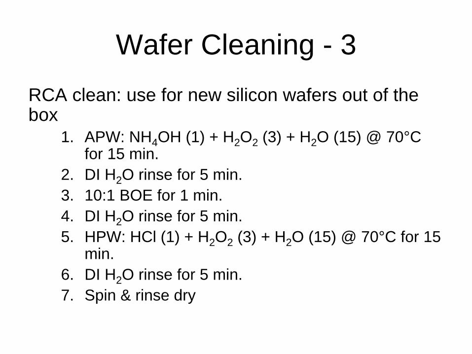
Wafer Cleaning - 3RCA clean: use for new silicon wafers out of the box
1. APW: NH4 OH (1) + H2 O2 (3) + H2 O (15) @ 70°C for 15 min.
2. DI H2 O rinse for 5 min.3. 10:1 BOE for 1 min.4. DI H2 O rinse for 5 min.5. HPW: HCl (1) + H2 O2 (3) + H2 O (15) @ 70°C for 15
min.6. DI H2 O rinse for 5 min.7. Spin & rinse dry
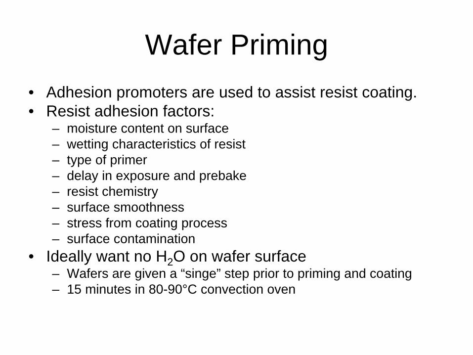
Wafer Priming• Adhesion promoters are used to assist resist coating.• Resist adhesion factors:
– moisture content on surface– wetting characteristics of resist– type of primer– delay in exposure and prebake– resist chemistry– surface smoothness– stress from coating process– surface contamination
• Ideally want no H2 O on wafer surface– Wafers are given a “singe” step prior to priming and coating– 15 minutes in 80-90°C convection oven
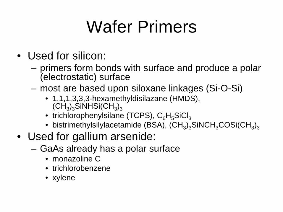
Wafer Primers• Used for silicon:
– primers form bonds with surface and produce a polar (electrostatic) surface
– most are based upon siloxane linkages (Si-O-Si)• 1,1,1,3,3,3-hexamethyldisilazane (HMDS),
(CH3 )3 SiNHSi(CH3 )3• trichlorophenylsilane (TCPS), C6 H5 SiCl3• bistrimethylsilylacetamide (BSA), (CH3 )3 SiNCH3 COSi(CH3 )3
• Used for gallium arsenide:– GaAs already has a polar surface
• monazoline C• trichlorobenzene• xylene
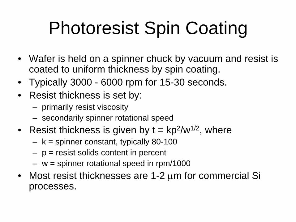
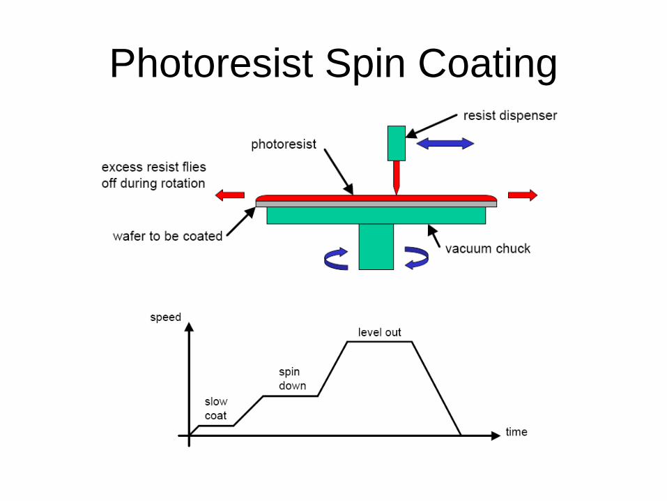
Photoresist Spin Coating• Wafer is held on a spinner chuck by vacuum and resist is
coated to uniform thickness by spin coating.• Typically 3000 - 6000 rpm for 15-30 seconds.• Resist thickness is set by:
– primarily resist viscosity– secondarily spinner rotational speed
• Resist thickness is given by t = kp2/w1/2, where– k = spinner constant, typically 80-100– p = resist solids content in percent– w = spinner rotational speed in rpm/1000
• Most resist thicknesses are 1-2 μm for commercial Si processes.
Photoresist Spin Coating
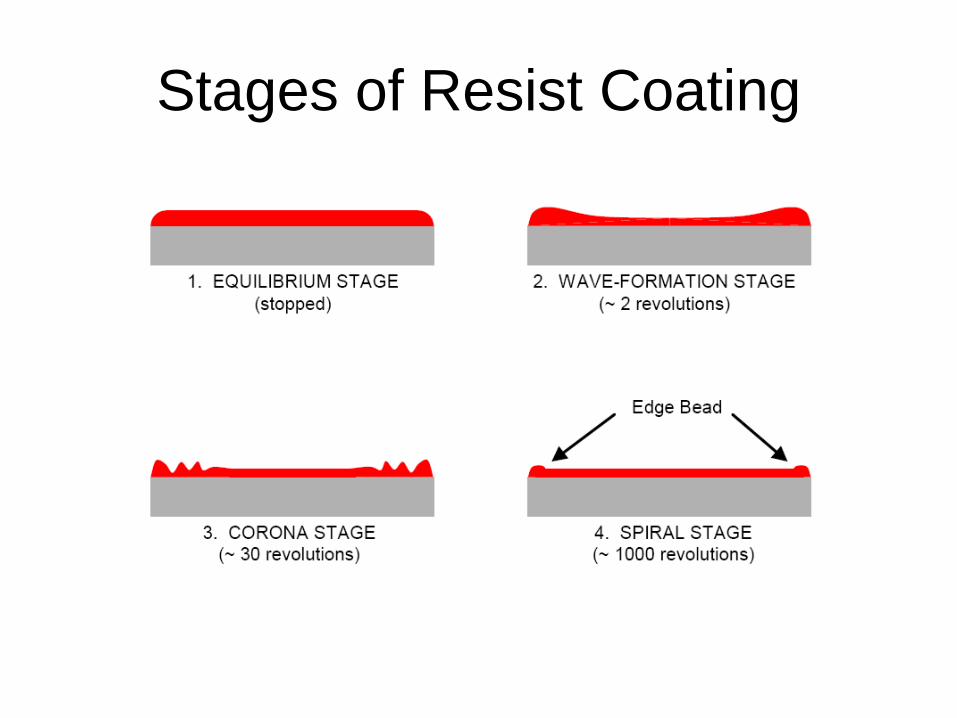
Stages of Resist Coating
Spinning Artifacts• Striations
– ~ 30 nm variations in resist thickness due to non-uniform drying of solvent during spin coating
– ~ 80-100 mm periodicity, radially out from center of wafer• Edge Bead
– residual ridge in resist at edge of wafer– can be up to 20-30 times the nominal thickness of the resist– radius on wafer edge greatly reduces the edge bead height– non-circular wafers greatly increase the edge bead height– edge bead removers are solvents that are spun on after resist
coating and which partially dissolve away the edge bead• Streaks
– radial patterns caused by hard particles whose diameter are greater than the resist thickness
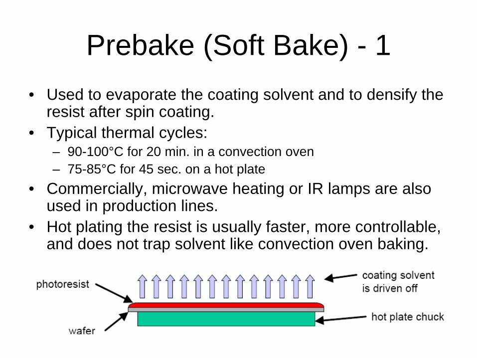
Prebake (Soft Bake) - 1• Used to evaporate the coating solvent and to densify the
resist after spin coating.• Typical thermal cycles:
– 90-100°C for 20 min. in a convection oven– 75-85°C for 45 sec. on a hot plate
• Commercially, microwave heating or IR lamps are also used in production lines.
• Hot plating the resist is usually faster, more controllable, and does not trap solvent like convection oven baking.
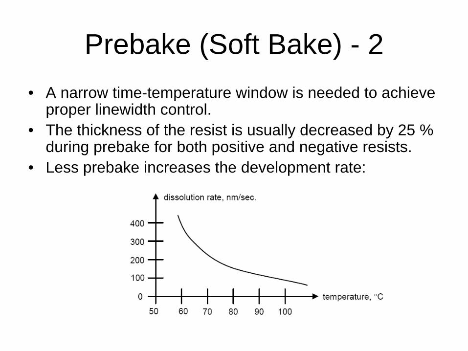
Prebake (Soft Bake) - 2• A narrow time-temperature window is needed to achieve
proper linewidth control.• The thickness of the resist is usually decreased by 25 %
during prebake for both positive and negative resists.• Less prebake increases the development rate:
Prebake (Soft Bake) - 3• Convection ovens:
– Solvent at surface of resist is evaporated first, which can cause resist to develop impermeable skin, trapping the remaining solvent inside
– Heating must go slow to avoid solvent burst effects• Conduction (hot plate):
– Need an extremely smooth surface for good thermal contact and heating uniformity
– Temperature rise starts at bottom of wafer and works upward, more thoroughly evaporating the coating solvent
– Generally much faster and more suitable for automation
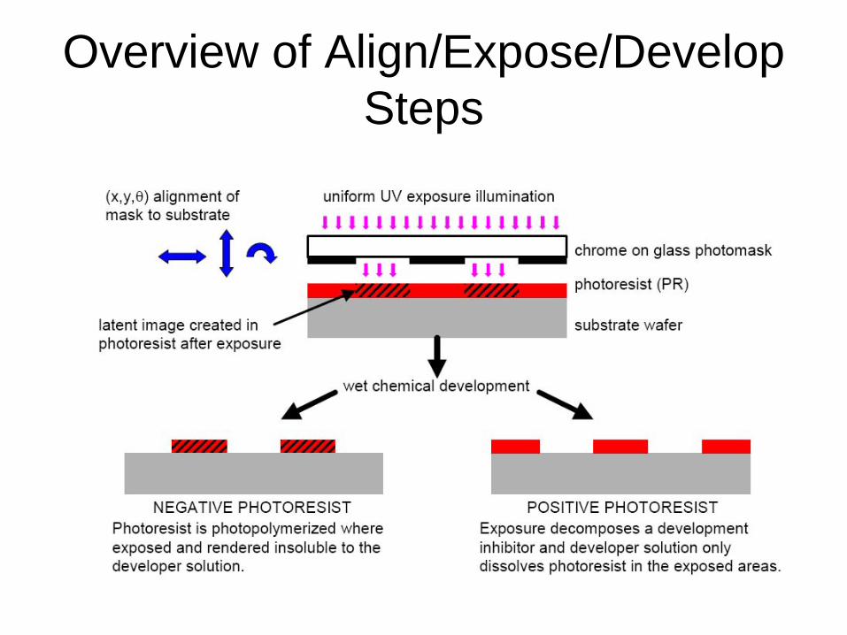
Overview of Align/Expose/Develop Steps
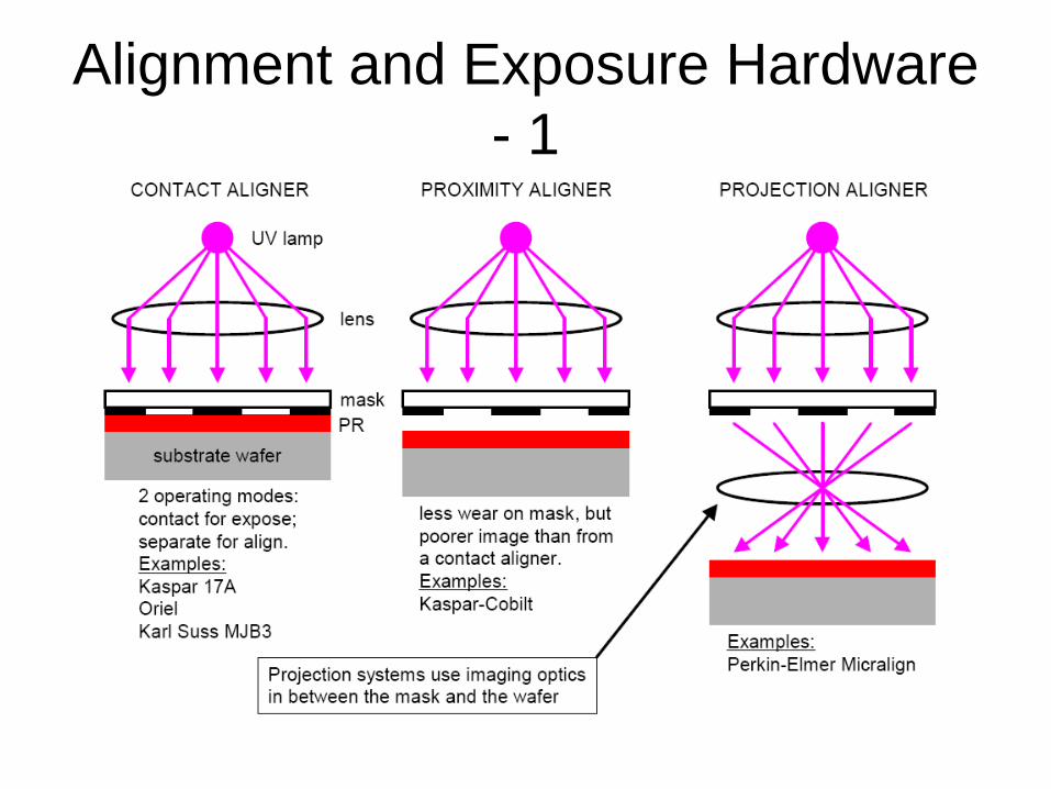
Alignment and Exposure Hardware - 1
Alignment and Exposure Hardware - 2
• For simple contact, proximity, and projection systems, the mask is the same size and scale as the printed wafer pattern. I.e. the reproduction ratio is 1:1.
• Projection systems give the ability to change the reproduction ratio. Going to 10:1 reduction allows larger size patterns on the mask, which is more robust to mask defects.
• Mask size can get unwieldy for large wafers.• Most wafers contain an array of the same pattern, so only one cell of
the array is needed on the mask. This system is called Direct Step on Wafer (DSW). These machines are also called “Steppers”
• Example: GCA-4800 (original machine)• Advantage of steppers: only 1 cell of wafer is needed• Disadvantage of steppers: the 1 cell of the wafer on the mask must
be perfect-- absolutely no defects, since it gets used for all die.

Alignment and Exposure Hardware - 3
• Higher end research systems go one step further and use Direct Write on Wafer (DWW) exposure systems.
• This can be accomplished using:– Excimer lasers for geometries down to 1-2 mm– Electron beams for geometries down to 0.1-0.2 mm– Focused ion beams for geometries down to 0.05-0.1
mm• No mask is needed for these technologies.• These are serial processes, and wafer cycle
time is proportional to the beam writing time-- the smaller the spot, the longer it takes!
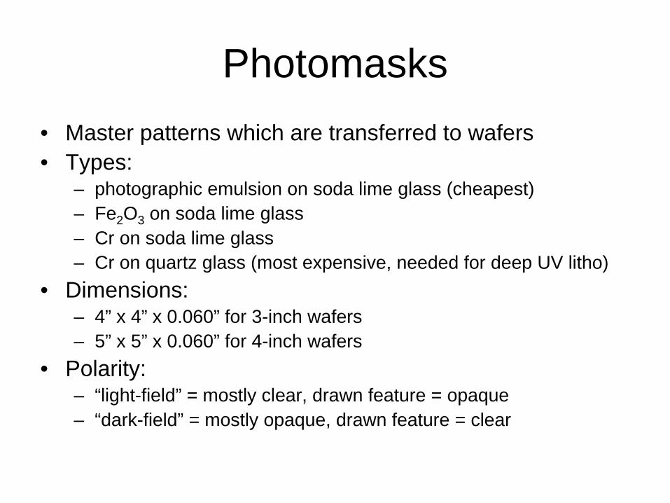
Photomasks• Master patterns which are transferred to wafers• Types:
– photographic emulsion on soda lime glass (cheapest)– Fe2 O3 on soda lime glass– Cr on soda lime glass– Cr on quartz glass (most expensive, needed for deep UV litho)
• Dimensions:– 4” x 4” x 0.060” for 3-inch wafers– 5” x 5” x 0.060” for 4-inch wafers
• Polarity:– “light-field” = mostly clear, drawn feature = opaque– “dark-field” = mostly opaque, drawn feature = clear
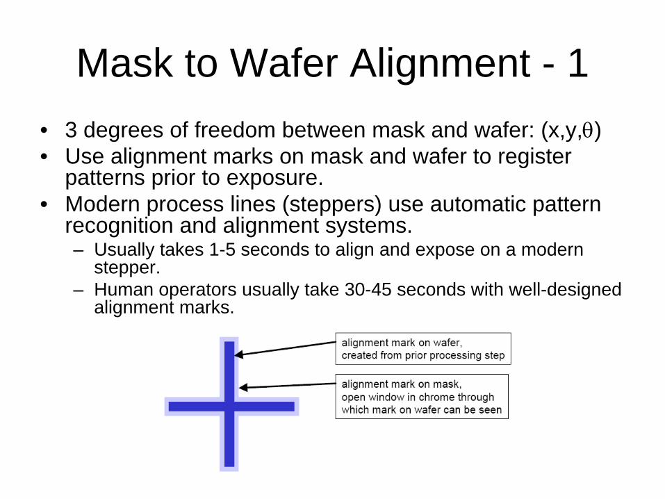
Mask to Wafer Alignment - 1• 3 degrees of freedom between mask and wafer: (x,y,θ)• Use alignment marks on mask and wafer to register
patterns prior to exposure.• Modern process lines (steppers) use automatic pattern
recognition and alignment systems.– Usually takes 1-5 seconds to align and expose on a modern
stepper.– Human operators usually take 30-45 seconds with well-designed
alignment marks.
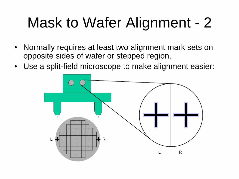
Mask to Wafer Alignment - 2• Normally requires at least two alignment mark sets on
opposite sides of wafer or stepped region.• Use a split-field microscope to make alignment easier:
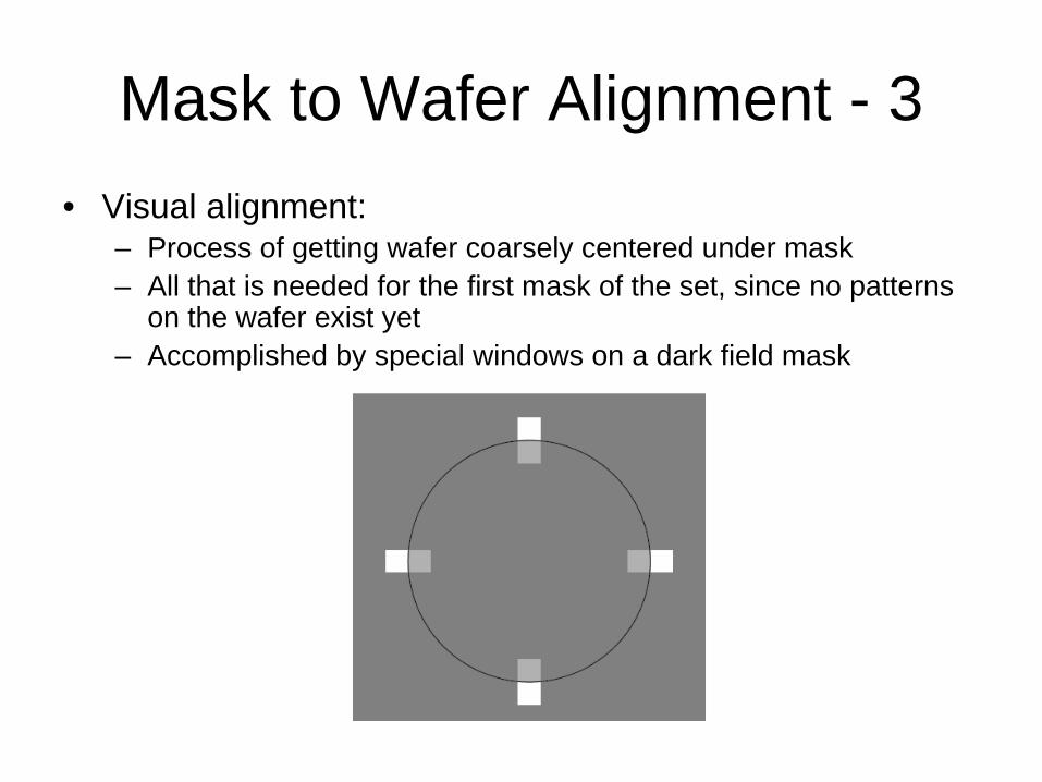
Mask to Wafer Alignment - 3• Visual alignment:
– Process of getting wafer coarsely centered under mask– All that is needed for the first mask of the set, since no patterns
on the wafer exist yet– Accomplished by special windows on a dark field mask
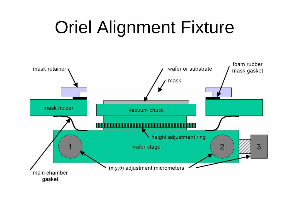
Oriel Alignment Fixture
Postbake (Hard Bake) - 1• Used to stabilize and harden the developed photoresist
prior to processing steps that the resist will mask.• Main parameter is the plastic flow or glass transition
temperature.• Postbake removes any remaining traces of the coating
solvent or developer.• This eliminates the solvent burst effects in vacuum
processing.• Postbake introduces some stress into the photoresist.• Some shrinkage of the photoresist may occur.• Longer or hotter postbake makes resist removal much
more difficult.
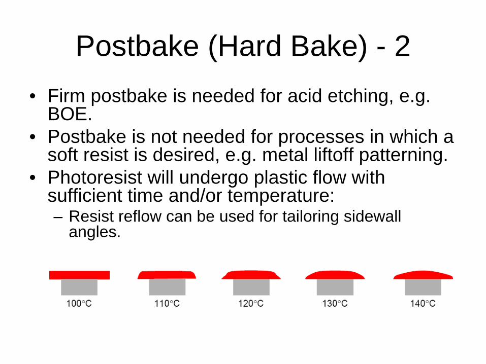
Postbake (Hard Bake) - 2• Firm postbake is needed for acid etching, e.g.
BOE.• Postbake is not needed for processes in which a
soft resist is desired, e.g. metal liftoff patterning.• Photoresist will undergo plastic flow with
sufficient time and/or temperature:– Resist reflow can be used for tailoring sidewall
angles.
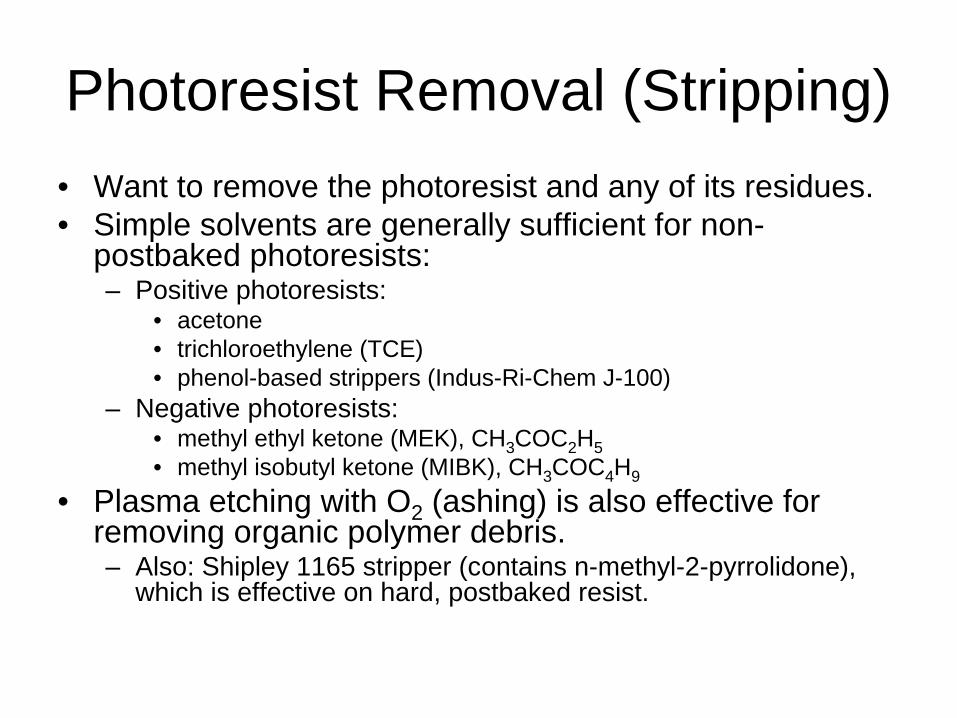
Photoresist Removal (Stripping)• Want to remove the photoresist and any of its residues.• Simple solvents are generally sufficient for non-
postbaked photoresists:– Positive photoresists:
• acetone• trichloroethylene (TCE)• phenol-based strippers (Indus-Ri-Chem J-100)
– Negative photoresists:• methyl ethyl ketone (MEK), CH3 COC2 H5• methyl isobutyl ketone (MIBK), CH3 COC4 H9
• Plasma etching with O2 (ashing) is also effective for removing organic polymer debris.– Also: Shipley 1165 stripper (contains n-methyl-2-pyrrolidone),
which is effective on hard, postbaked resist.
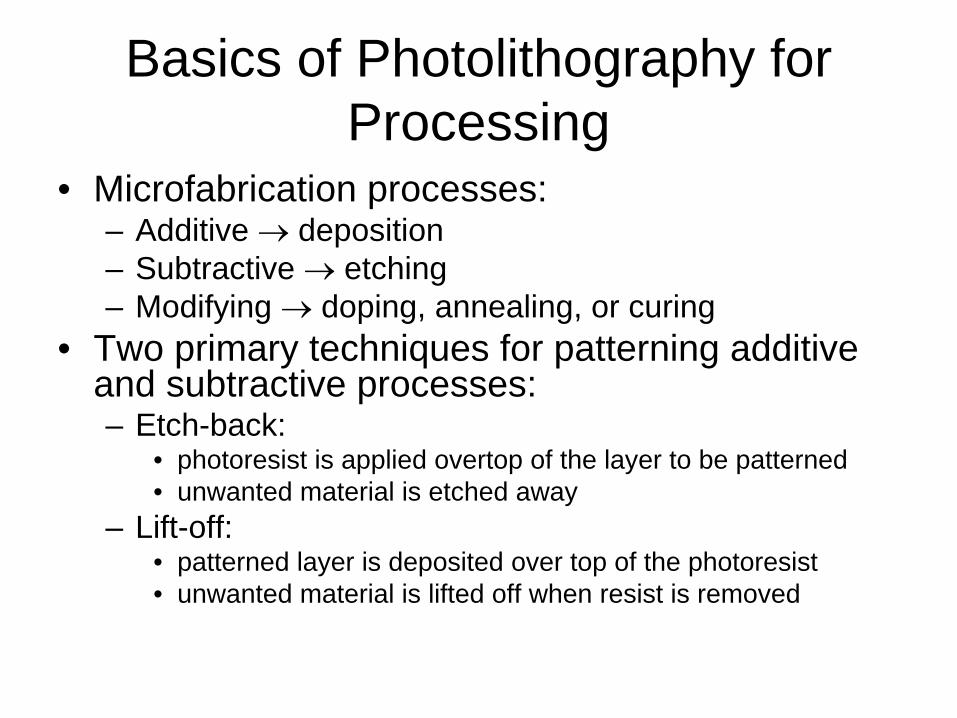
Basics of Photolithography for Processing
• Microfabrication processes:– Additive → deposition– Subtractive → etching– Modifying → doping, annealing, or curing
• Two primary techniques for patterning additive and subtractive processes:– Etch-back:
• photoresist is applied overtop of the layer to be patterned• unwanted material is etched away
– Lift-off:• patterned layer is deposited over top of the photoresist• unwanted material is lifted off when resist is removed
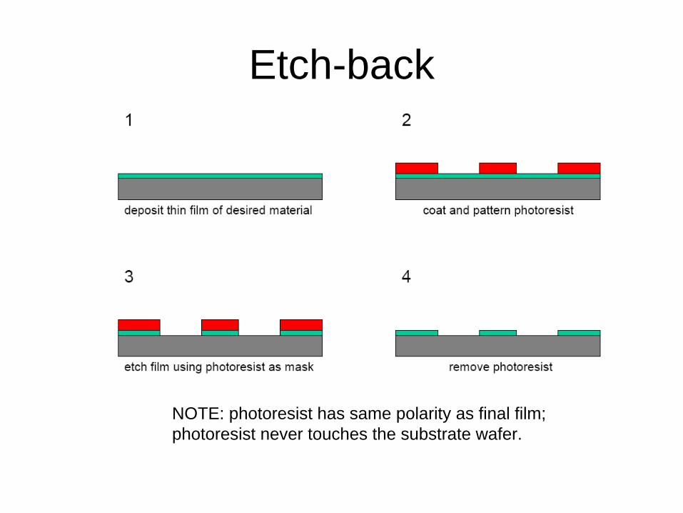
Etch-back
NOTE: photoresist has same polarity as final film;photoresist never touches the substrate wafer.
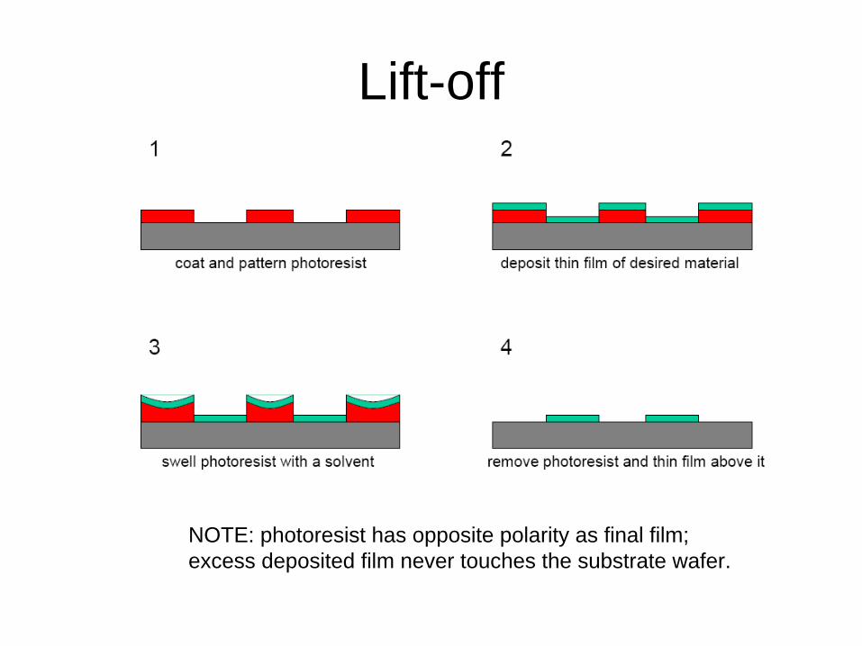
Lift-off
NOTE: photoresist has opposite polarity as final film;excess deposited film never touches the substrate wafer.
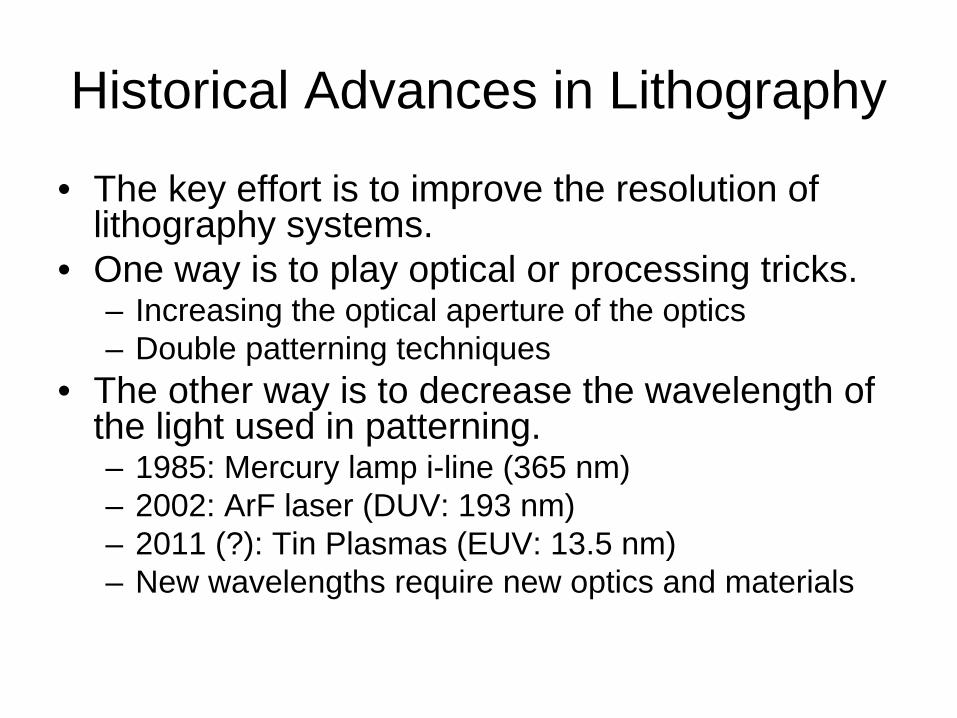
Historical Advances in Lithography
• The key effort is to improve the resolution of lithography systems.
• One way is to play optical or processing tricks.– Increasing the optical aperture of the optics– Double patterning techniques
• The other way is to decrease the wavelength of the light used in patterning.– 1985: Mercury lamp i-line (365 nm)– 2002: ArF laser (DUV: 193 nm)– 2011 (?): Tin Plasmas (EUV: 13.5 nm)– New wavelengths require new optics and materials
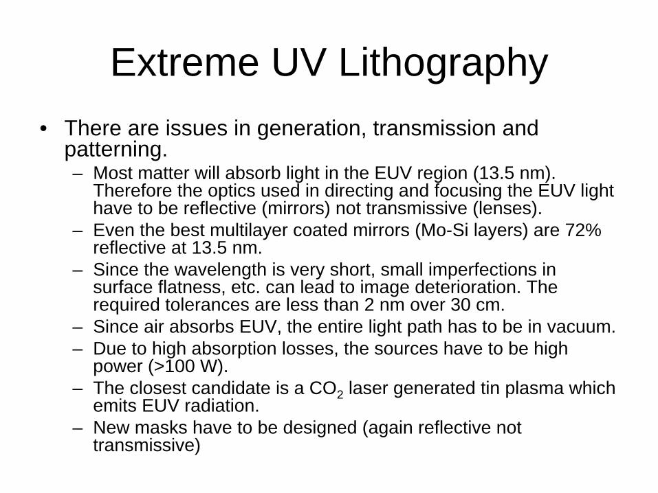
Extreme UV Lithography• There are issues in generation, transmission and
patterning.– Most matter will absorb light in the EUV region (13.5 nm).
Therefore the optics used in directing and focusing the EUV light have to be reflective (mirrors) not transmissive (lenses).
– Even the best multilayer coated mirrors (Mo-Si layers) are 72% reflective at 13.5 nm.
– Since the wavelength is very short, small imperfections in surface flatness, etc. can lead to image deterioration. The required tolerances are less than 2 nm over 30 cm.
– Since air absorbs EUV, the entire light path has to be in vacuum.– Due to high absorption losses, the sources have to be high
power (>100 W).– The closest candidate is a CO2 laser generated tin plasma which
emits EUV radiation.– New masks have to be designed (again reflective not
transmissive)


![[docx] Of Cleaving to God: De adhaerendo Deo](https://static.fdocuments.net/doc/165x107/58832e7b1a28abaf6f8b48dd/docx-of-cleaving-to-god-de-adhaerendo-deo.jpg)


