Photo Luminescence of Surfaces and Interfaces
26
Photoluminescence in Analysis of Surfaces and Interfaces Timoth y H. Gfroere r in Encyclopedia of Analytical Chemistry R.A. Meyers (Ed.) pp. 9209–9231 © John Wiley & Sons Ltd, Chichester, 2000
-
Upload
nick-keller -
Category
Documents
-
view
221 -
download
0
Transcript of Photo Luminescence of Surfaces and Interfaces

8/8/2019 Photo Luminescence of Surfaces and Interfaces
http://slidepdf.com/reader/full/photo-luminescence-of-surfaces-and-interfaces 1/25
Photoluminescence in Analysis of Surfaces and Interfaces
Timothy H. Gfroerer
inEncyclopedia of Analytical Chemistry
R.A. Meyers (Ed.)
pp. 9209–9231
© John Wiley & Sons Ltd, Chichester, 2000

8/8/2019 Photo Luminescence of Surfaces and Interfaces
http://slidepdf.com/reader/full/photo-luminescence-of-surfaces-and-interfaces 2/25

8/8/2019 Photo Luminescence of Surfaces and Interfaces
http://slidepdf.com/reader/full/photo-luminescence-of-surfaces-and-interfaces 3/25
PHOTOLUMINESCENCE IN ANALYSIS OF SURFACES AND INTERFACES 1
Photoluminescence in Analysis
of Surfaces and InterfacesTimothy H. Gfroerer
Davidson College, Davidson, USA
1 Introduction 1
2 Photoluminescence Excitation 32.1 Excitation Energy: Penetration
Depth and Stoke’s Shift 32.2 Excitation Intensity: Interface State
Density and Distribution 43 Photoluminescence Spectrum 7
3.1 Photoluminescence Peak Positions:Energy Levels 8
3.2 Photoluminescence Line Widthand Splitting: Alloy Disorder andInterface Roughness 10
4 Photoluminescence Intensity 124.1 Dependence on Applied Bias:
Surface Potential 134.2 Spatial Dependence: Interface
Uniformity and Carrier Diffusion 14
4.3 Time Dependence: RecombinationRates 164.4 Temperature Dependence: Thermal
Population 18
5 Photoluminescence Polarization 19
6 Conclusion 20
Abbreviations and Acronyms 20
Related Articles 21
References 21
Photoluminescence (PL) is the spontaneous emission
of light from a material under optical excitation. The
excitation energyand intensity are chosento probe different
regions and excitation concentrations in the sample. PL
investigations can be used to characterize a variety of
material parameters. PL spectroscopy provides electrical
(as opposed to mechanical) characterization, and it is a
selectiveand extremelysensitive probeof discrete electronic
states. Features of the emission spectrum can be used to
identify surface, interface, and impurity levels and to gauge
alloy disorder and interface roughness. The intensity of the
PL signal provides information on the quality of surfaces
and interfaces. Under pulsed excitation, the transient PL
intensity yields the lifetime of nonequilibrium interface and
bulk states. Variation of the PL intensity under an applied
bias can be used to map the electric field at the surface of
a sample. In addition, thermally activated processes causechanges in PL intensity with temperature.
PL analysis is nondestructive. Indeed, the technique
requires very little sample manipulation or environ-
mental control. Because the sample is excited optically,
electrical contacts and junctions are unnecessary and
high-resistivity materials pose no practical difficulty. In
addition, time-resolved PL can be very fast, making it
useful for characterizing the most rapid processes in a
material. The fundamental limitation of PL analysis is its
reliance on radiative events. Materials with poor radiative
efficiency, such as low-quality indirect bandgap semicon-
ductors, are difficult to study via ordinary PL. Similarly,identification of impurity and defect states depends on their
optical activity. Although PL is a very sensitive probe of
radiative levels, one must rely on secondary evidence to
study states that couple weakly with light.
1 INTRODUCTION
Multilayer material systems are increasingly importantin the development of smaller, faster, and more efficientelectronic and optoelectronic devices. The primary moti-
vation for using multilayer structures is to change thepotential energy of electrons and holes at the materialinterfaces. Because phenomena at surfaces and interfacestend to dominate the behavior of excitations in theseheterostructures, the performance of many microelec-tronic devices is limited by the nature of heterojunctions.Smooth and atomically abrupt interfaces are necessaryfor good optical and electrical reflection, uniform quan-tum confinement, and high carrier mobility. Even moreimportantly, defects and impurities at interfaces providenew states for electrons and holes, altering their motion,lifetime, and transition energies.
When light of sufficient energy is incident on amaterial, photons are absorbed and electronic excitationsare created. Eventually, these excitations relax andthe electrons return to the ground state. If radiativerelaxation occurs, the emitted light is called PL. Thislight can be collected and analyzed to yield a wealth of information about the photoexcited material. The PLspectrum provides the transition energies, which canbe used to determine electronic energy levels. The PLintensity gives a measure of the relative rates of radiativeand nonradiative recombination. Variation of the PLintensity with external parameters like temperature andapplied voltage can be used to characterize further the
underlying electronic states and bands.
Encyclopedia of Analytical Chemistry
R.A. Meyers (Ed.) Copyright © John Wiley & Sons Ltd

8/8/2019 Photo Luminescence of Surfaces and Interfaces
http://slidepdf.com/reader/full/photo-luminescence-of-surfaces-and-interfaces 4/25
2 SURFACES
PL depends on the nature of the optical excitation.The excitation energy selects the initial photoexcitedstate and governs the penetration depth of the incident
light. The PL signal often depends on the density of photoexcited electrons, and the intensity of the inci-dent beam can be adjusted to control this parameter.When the type or quality of material under investi-gation varies spatially, the PL signal will change withexcitation position. In addition, pulsed optical exci-tation provides a powerful means for studying tran-sient phenomena. Short laser pulses produce virtuallyinstantaneous excited populations, after which the PLsignal can be monitored to determine recombinationrates.
Because PL often originates near the surface of
a material, PL analysis is an important tool in thecharacterization of surfaces. The utility of PL forthis purpose is derived from its unique sensitivityto discrete electronic states, many of which lie nearsurfaces and interfaces. Using the techniques notedabove, the nature of these states can be probed indetail. The energy distribution and density of interfacestates can be ascertained by studying the excitationintensity dependence of the PL spectrum. The presenceof surface adsorbates alters the intensity of the PLsignal. When the states serve as long-lived traps, thedepth of the trap can be determined by observingthermal activation in temperature-dependent PL. Infact, even if interface states are nonradiative, which isusually the case, the states alter the time-resolved PLof radiative transitions in the material. Nonradiativetraps dominate the transient PL signal at low carrierdensity.
PL is simple, versatile, and nondestructive. The instru-mentation that is required for ordinary PL work ismodest: an optical source and an optical power meteror spectrophotometer. A typical PL set-up is shown inFigure 1. Because the measurement does not rely onelectrical excitation or detection, sample preparationis minimal. This feature makes PL particularly attrac-
tive for material systems having poor conductivity orundeveloped contact/junction technology. Measuring the
Laser
Spectrometer
Lens
Sample
Photo-detector PL
Figure 1 Typical experimental set-up for PL measurements.
continuous wave PL intensity and spectrum is quickand straightforward. On the other hand, investigatingtransient PL is more challenging, especially if recombina-
tion processes are fast. Instrumentation for time-resolveddetection, such as single photon counting, can be expen-sive and complex. Even so, PL is one of the onlytechniques available for studying fast transient behaviorin materials.
Because PL can be used to study virtually any surfacein any environment, it can be used to monitor changesinduced by surface modification in real time. For exam-ple, unlike most surface characterization techniques, PLis generally not sensitive to the pressure in the samplechamber. Hence, it can be used to study surface prop-erties in relatively high-pressure semiconductor growth
reactors. Although PL does depend quite strongly on tem-perature, liquid helium temperatures being required forthe highest spectral resolution, room-temperature mea-surements are sufficient for many purposes. In addition,PL has little effect on the surface under investigation.Photoinduced changes and sample heating are possible,but low excitation can minimize these effects. In situPL measurements do require optical access to the sam-ple chamber. Yet, compared with other optical methodsof characterization like reflection and absorption, PL isless stringent about beam alignment, surface flatness, andsample thickness.
The advantages of PL analysis listed above derive fromthe simplicity of optical measurements and the powerto probe fundamental electronic properties. The chief drawback of PL analysis also follows from the reliance onoptical techniques: the sample under investigation mustemit light. Indirect-bandgap semiconductors, where theconduction band minimum is separated from the valenceband maximum in momentum space, have inherentlylow PL efficiency. Nonradiative recombination tendsto dominate the relaxation of excited populations inthese materials. This problem can be augmented bypoor surface quality, where rapid nonradiative eventsmay occur. Nevertheless, once a PL signal is detected,
it can be used to characterize both radiative andnonradiative mechanisms. Although it may not bepossible to identify directly the nonradiative traps viaPL, their signature is evident in several types of PLmeasurements.
Another shortcoming of PL is the difficulty in estimat-ing the density of interface and impurity states. Whenthese states have radiative levels, they are readily iden-tified in the PL spectrum, and the size of the associatedPL peaks provides a relative measure of their presencein the sample. However, measuring the absolute densityof these states is a far more formidable task and typically
requires an exhaustive analysis of the excitation intensitydependence of the PL signal.

8/8/2019 Photo Luminescence of Surfaces and Interfaces
http://slidepdf.com/reader/full/photo-luminescence-of-surfaces-and-interfaces 5/25
PHOTOLUMINESCENCE IN ANALYSIS OF SURFACES AND INTERFACES 3
2 PHOTOLUMINESCENCE EXCITATION
The choice of excitation is critical in any PL measurement.The excitation energy and intensity will have profoundeffects on the PL signal. Although the excitation condi-tions must be considered carefully, the strength of thePL technique relies heavily on the flexibility that theseadjustable parameters provide. Because the absorptionof most materials depends on energy, the penetrationdepth of the incident light will depend on the excitationwavelength. Hence, different excitation energies probedifferent regions of the sample. The excitation energyalso selects the initial excited state in the experiment.Because lasers are monochromatic, intense, and readilyfocused, they are the instruments of choice for photolu-
minescence excitation (PLE). For many applications, theexcitation energy is not critical. Here, a relatively inex-pensive HeNe or diode laser will often satisfy the basicrequirement of light exceeding the bandgap energy. Inmore demanding experiments, the laser is chosen care-fully to probe a particular depth or to excite a particularspecies in the sample.
Unlike the excitation energy, which may or may notbe important, the excitation intensity will influence theresult of any PL experiment. The excitation intensity con-trols the density of photoexcited electrons and holes,which governs the behavior of these carriers. Each
electron–hole recombination mechanism has a distinctfunctional dependence on carrier density. For example,the number of interface and impurity states is finite, andrecombination at these sites will saturate at high exci-tation. In addition, the photoexcited carriers themselvescan alter the distribution of interface states. Thus, theexcitation intensity must be calibrated accurately andcontrolled precisely.
2.1 Excitation Energy: Penetration Depth and Stoke’sShift
The absorption of a material depends strongly on the
energy of the incident light. In the analysis of surfaces, it isuseful to describe this wavelength-dependent absorptionby a penetration depth (the inverse of the absorptioncoefficient), which is a measure of the thickness of thelayer that is probed. In direct-bandgap semiconductors,above-bandgap excitation has a penetration depth of theorder of 1 µm. The diffusion of photoexcited carrierscan vary widely but is typically in the range 1–10 µm.Hence, PL with above-gap excitation is very sensitive tosurface effects. In indirect-bandgap semiconductors, ordirect-gap semiconductors with sub-bandgap excitation,absorption is weaker and the light penetrates deeper
into the sample. Here, the PL is dominated by bulkrecombination. If multiple excitation wavelengths are
available, this property of PL can be used to distinguishsurface and bulk contributions.
Garcia-Garcia et al. have used such an approach to
study the surface layer of chemically etched CdTe.1
When the surface structure is poor, the PL spec-trum changes with increasing excitation energy, thestrength of defect-related lines increasing relative tobulk features. Correlation of these changes with pen-etration depth indicates the location of near-surfacedefects. Furthermore, the authors found that the PLspectrum of a high-quality surface is independent of excitation energy. In an extension of this technique,Wang et al. used the widely divergent penetration of one and two photon absorption processes to distin-guish surface and bulk effects.2 In contrast to relatively
slow recombination with two-photon excitation, a fastrecombination mechanism dominated the one-photonexcitation experiment. This result indicates the pres-ence of rapid recombination sites near the surface of the semiconductor, where the single-photon excitation isabsorbed.
Dangling bonds at a semiconductor surface or interfacegive rise to electronic states within the bandgap. Thesemid-gap states fill up to the Fermi level with electrons thatoriginate in the bulk of the material. The accumulationof charge at the surface creates an electric field – adepletion region – that leads to bending of the valenceand conduction band edges. According to a simple dead-layer model,3 electron–hole pairs that are generated inthis region are swept apart by the electric field, prohibitingradiative recombination. The phenomenon is describedquantitatively by a depletion thickness that characterizesthis ‘‘dead layer’’.
Although the dead-layer picture of carrier kineticsat the surface of a semiconductor overlooks the com-plicated role of surface states in the recombinationprocess, it is useful when PL quenching has an elec-trostatic origin. For example, Ryswyk and Ellis havestudied the effect of I2 on n-GaAs in the context of this model.4 They used PL depth profiling with mul-
tiple excitation wavelengths to determine the depletionthickness in the I2-treated sample. Uosaki et al.5 haveused a similar experimental approach to characterize p-GaAs/electrolyte interfaces. Results were analyzed withinthe context of the more sophisticated model proposed byMettler,6 which accounts for changes in charge sep-aration and surface state recombination. It should benoted that these phenomena are intricately connected,and resolving their contributions to PL quenching is diffi-cult. Although changes in the electric field at the surfaceshould not affect the surface state density, altering thenature or number of surface states can affect depletion
and band bending. This point will be discussed in moredetail in section 4.

8/8/2019 Photo Luminescence of Surfaces and Interfaces
http://slidepdf.com/reader/full/photo-luminescence-of-surfaces-and-interfaces 6/25
4 SURFACES
In addition to controlling the penetration depth,the excitation energy selects the initial photoexcitedstate in the sample. This state is short-lived because
thermalization of photoexcited carriers via phononemission is rapid. Relaxation to within kT of thelowest available states is usually orders of magnitudefaster than recombination. Thus, ordinary PL emissiononly reveals the lowest energy states. Nevertheless, itis possible to obtain spectral information on excitedstates by collecting the low-energy emission while tuningthe excitation energy across higher energy states. ThePL signal is enhanced when the excitation energy isresonant with an excited state. The technique, calledphotoluminescence excitation spectroscopy, is similar toordinary absorption subject to the condition that there
exists a relaxation channel from the excited state to theemission state being monitored. PLE is frequently used tostudy epilayers on opaque substrates because absorptionis not feasible in this case.
Compared to band continua, discrete interface statesare relatively sparse. PL is easily dominated by interfacestates because such states tend to have levels belowthe intrinsic bands, and carriers are remarkably efficientat finding the lowest available states. However, PLErelies on optical absorption, which is relatively weak forisolated interface sites. Hence, it is usually difficult touncover interface states in PLE spectra. Nevertheless,PLE has been applied successfully to the characterizationof certain surface species. For example, Zhu et al. utilizedPLE to identify groups chemisorbed on the surface of TiO2 ultrafine particles.7 Similarly, Anpo et al. usedthe dependence of PL on excitation energy to resolvedifferences between anchored and impregnated Mo/SiO2
catalysts.8
An important feature of optical transitions in semi-conductor quantum wells (QWs) is the energy differ-ence between the absorption (or PLE) and emissionpeaks – Stoke’s shift. This shift is a measure of interfacefluctuations because it indicates that the thickness of theQW varies with position. Carriers are photoexcited uni-
formly in the QW but they diffuse to regions of larger wellwidth, where the confinement energy is smaller, beforerecombining. Deveaud et al. have studied the PL andPLE spectra of a series of multiple QW samples.9 Insamples prepared under optimal growth conditions, theyobserved two sharp PL peaks, which they attribute torecombination in regions where the QW thickness dif-fers by exactly one atomic monolayer. PLE is used totest whether excitation at the higher energy peak yieldsemission from the lower energy peak and to confirm thatthermalization between the two regions occurs. It hasbeen argued that splittings in PL from QWs like those
discussed above can be misleading because impurities canproduce similar effects.10 The ambiguity can be resolved
by using PLE where impurity transitions are weak. Thestructure in PL spectra from QWs will be discussed inmore detail in section 3.2.
2.2 Excitation Intensity: Interface State Densityand Distribution
The intensity of the incident light controls a critical prop-erty of the PL experiment: the density of photoexcitedelectrons and holes. When the carrier density is low, themeasurement is dominated by discrete defect and impu-rity sites at the interfaces and within the bulk of thematerial. Recombination at these energetically favoredsites is frequently referred to as Shockley–Read–Hall(SRH) recombination, in recognition of early work on
the statistics of this phenomenon. The SRH rate is pro-portional to the dominant carrier density n. The dominantcarrier density is the greater of two quantities: the equilib-rium carrier concentration (i.e. the doping level) and thephotoexcited carrier concentration. Under intermediateexcitation, the discrete states are filled and bulk radiativerecombination plays a greater role. Neglecting excitoniceffects, these transitions are two-body events betweenfree electrons and holes, so the radiative rate varies asn2. It should be noted that low temperatures or quantumconfinement canmake Coulomb binding of electron– holepairs energetically favorable, leading to the formation of excitons that recombine radiatively at a rate proportionalto n. At the highest carrier densities, three-body Augerrecombination becomes important because the rate of this mechanism varies as n3. In the analysis of interfaces,the transition between SRH and radiative recombinationis the most important because it depends on the densityof defect and impurity sites.
In systems with high interface-to-volume ratios andactive layers that are thin relative to the carrier diffusionlength, interface effects dominate SRH recombination.In planar structures, the interface-to-volume dependenceof SRH recombination can be separated from actualinterface phenomena via the interface recombination
velocity S. The interface recombination rate is definedas Rs D S/dn, where d is the thickness of the opticallyactive layer. When two interfaces are present, as in adouble heterostructure, the two interface contributionsare combined: S is replaced by S1 C S2 (or 2S forequivalent interfaces). Because S is independent of carrierdensity and layer thickness, it can be used to compareinterface recombination in a variety of materials. S
depends strongly on the nature of the interface. Forexample, S is of the order of 107 cm s1 at the interfaceof GaAs and air, whereas high-quality GaAs/GaInPinterfaces can have S < 10cms1.11
This reduction of the interface recombination velocityat the edge of a material is called surface passivation.
8/8/2019 Photo Luminescence of Surfaces and Interfaces
http://slidepdf.com/reader/full/photo-luminescence-of-surfaces-and-interfaces 7/25
PHOTOLUMINESCENCE IN ANALYSIS OF SURFACES AND INTERFACES 5
Because the performance of many optoelectronic devicesis limited by interface recombination, interface passiva-tion has been studied extensively. Passivation techniques
include epitaxial growth of lattice-matched semiconduc-tor alloys and a variety of chemical surface treatments.Qualitative evaluation of these techniques is straightfor-ward: an increase in the PL signal indicates a decrease innonradiative interface recombination. Quantitative infor-mationon S requires more sophisticated techniques,manyof which involve investigations of the excitation intensitydependence of PL.
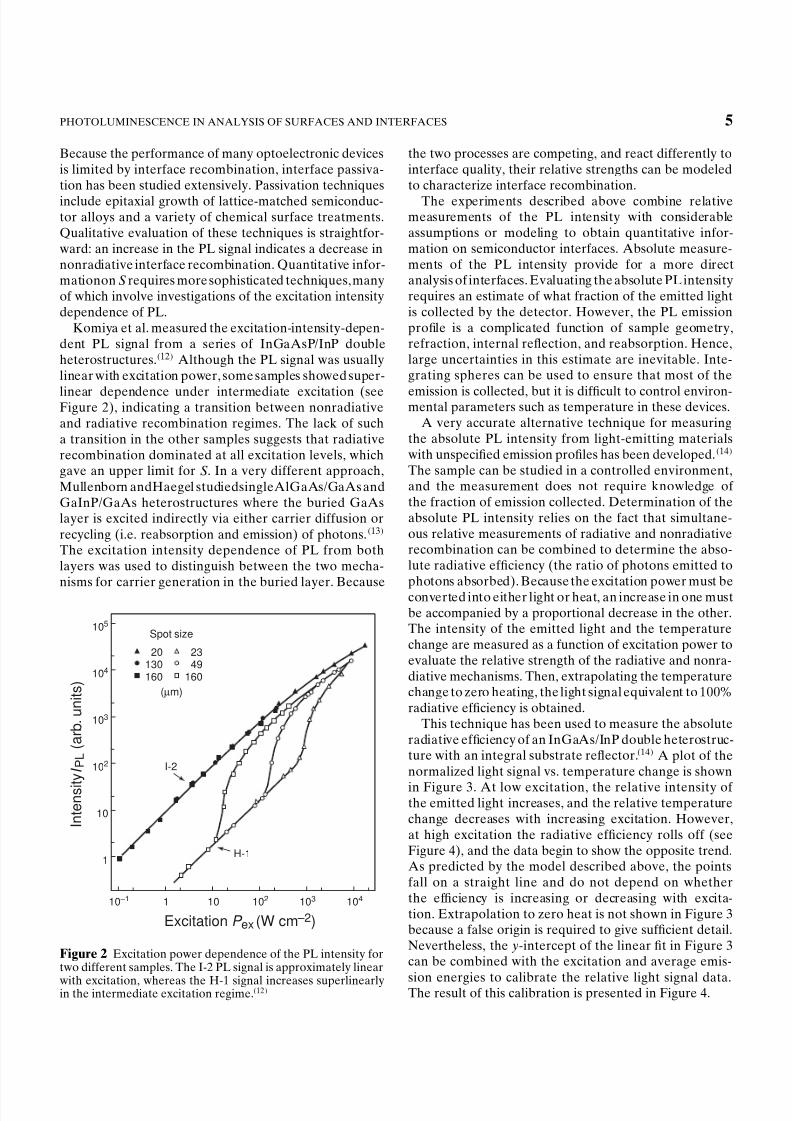
Komiya et al. measured the excitation-intensity-depen-dent PL signal from a series of InGaAsP/InP doubleheterostructures.12 Although the PL signal was usuallylinear with excitation power, some samples showed super-
linear dependence under intermediate excitation (seeFigure 2), indicating a transition between nonradiativeand radiative recombination regimes. The lack of sucha transition in the other samples suggests that radiativerecombination dominated at all excitation levels, whichgave an upper limit for S. In a very different approach,Mullenborn andHaegel studiedsingleAlGaAs/GaAs andGaInP/GaAs heterostructures where the buried GaAslayer is excited indirectly via either carrier diffusion orrecycling (i.e. reabsorption and emission) of photons. 13
The excitation intensity dependence of PL from bothlayers was used to distinguish between the two mecha-nisms for carrier generation in the buried layer. Because
10 –1
Spot size
1 10
Excitation P ex (W cm –2)
1
10
102
103
104
105
I n t e n s i t y I P L ( a r b . u n i t s )
102 103 104
20130160
I-2
H-1
(µm)
2349
160
Figure 2 Excitation power dependence of the PL intensity fortwo different samples. The I-2 PL signal is approximately linear
with excitation, whereas the H-1 signal increases superlinearlyin the intermediate excitation regime.12
the two processes are competing, and react differently tointerface quality, their relative strengths can be modeledto characterize interface recombination.
The experiments described above combine relativemeasurements of the PL intensity with considerableassumptions or modeling to obtain quantitative infor-mation on semiconductor interfaces. Absolute measure-ments of the PL intensity provide for a more directanalysis of interfaces. Evaluating the absolute PL intensityrequires an estimate of what fraction of the emitted lightis collected by the detector. However, the PL emissionprofile is a complicated function of sample geometry,refraction, internal reflection, and reabsorption. Hence,large uncertainties in this estimate are inevitable. Inte-grating spheres can be used to ensure that most of the
emission is collected, but it is difficult to control environ-mental parameters such as temperature in these devices.
A very accurate alternative technique for measuringthe absolute PL intensity from light-emitting materialswith unspecified emission profiles has been developed.14
The sample can be studied in a controlled environment,and the measurement does not require knowledge of the fraction of emission collected. Determination of theabsolute PL intensity relies on the fact that simultane-ous relative measurements of radiative and nonradiativerecombination can be combined to determine the abso-lute radiative efficiency (the ratio of photons emitted tophotons absorbed). Because the excitation power must beconverted into either light or heat, an increase in one mustbe accompanied by a proportional decrease in the other.The intensity of the emitted light and the temperaturechange are measured as a function of excitation power toevaluate the relative strength of the radiative and nonra-diative mechanisms. Then, extrapolating the temperaturechange to zero heating, the light signal equivalent to 100%radiative efficiency is obtained.
This technique has been used to measure the absoluteradiative efficiency of an InGaAs/InP double heterostruc-ture with an integral substrate reflector.14 A plot of thenormalized light signal vs. temperature change is shown
in Figure 3. At low excitation, the relative intensity of the emitted light increases, and the relative temperaturechange decreases with increasing excitation. However,at high excitation the radiative efficiency rolls off (seeFigure 4), and the data begin to show the opposite trend.As predicted by the model described above, the pointsfall on a straight line and do not depend on whetherthe efficiency is increasing or decreasing with excita-tion. Extrapolation to zero heat is not shown in Figure 3because a false origin is required to give sufficient detail.Nevertheless, the y-intercept of the linear fit in Figure 3can be combined with the excitation and average emis-
sion energies to calibrate the relative light signal data.The result of this calibration is presented in Figure 4.

8/8/2019 Photo Luminescence of Surfaces and Interfaces
http://slidepdf.com/reader/full/photo-luminescence-of-surfaces-and-interfaces 8/25
6 SURFACES
100 120 140 160
40
50
60
70
80
90
Increasingexcitation
F r a c t i o n a l l u m i n e s c e n c e
Fractional heating
Figure 3 Relative measurements of luminescence signal andtemperature change, normalized by the excitation intensity andplotted against each other. The dotted line indicates how the
result evolves as the excitation power is increased.14
The fit in Figure 4 relies on the fact that, in steadystate, the rate of carrier generation equals the rate of recombination, as shown in Equation (1):
P abs
EexD V
2S
dnC
B
N n2CCn3 1
Here, P abs is the absorbed laser power, Eex is the laserenergy, and V is the volume. The photon recycling factorN is the average number of radiative recombinationevents required for a photon to escape the semiconductor,
and B and C are parameters that describe the rates of radiative and Auger recombination respectively. Becausethe fit is very sensitive to the coefficients that characterizethe different mechanisms for recombination, it canbe used to evaluate parameters such as the interfacerecombination velocity S.
Saitoh et al. have argued that the simple picture of anexcitation-independent surface recombination velocity isnot sufficient to describe the excitation dependence of thePL signal.15 In particular, when the excitation is inter-mediate between the SRH and radiative recombination-dominated regimes, the quasi-Fermi levels for electrons
and holes split away from the low-excitation pinned posi-tion and move toward their respective band edges. The
30
40
50
60
70
1015
1016
1017
1014
E
x t e r n a l e f f i c i e n c y ( % )
Electron−hole pair generation/ recombination (s−1)
Figure 4 External radiative quantum efficiency vs. the rate
of electron–hole pair generation and recombination in steadystate. The solid line is a fit to the data that accounts for interface,radiative, and Auger recombination events.14
quasi-Fermi levels determine the energy range of sur-face states that contribute to recombination. Thus, thePL efficiency in this transition region is very sensitiveto the density and energy distribution of surface states.The authors have developed an elaborate model of car-rier behavior near the surface of the semiconductorthat accounts for carrier transport, surface state occu-pation, band bending, and recombination. Analysis of the excitation-intensity-dependent PL signal in the con-
text of this model is referred to as photoluminescencesurface-state spectroscopy (PLS3).
The shape of the radiative efficiency curve in the SRHto radiative recombination transition region dependson the distribution of surface states that participate inrecombination. If the distribution consists of a discreteset of states with similar energetic positions within the gap,complete saturation of the SRH recombination processwill lead to a PL efficiency slope of unity. Efficiency curveswith slopes less than unity indicate that the surface-statedistribution is continuous and that an increasing numberof surface states are participating in recombination
as the quasi-Fermi levels move through the bandgap.Hence, variation in the slope of the efficiency curve with

8/8/2019 Photo Luminescence of Surfaces and Interfaces
http://slidepdf.com/reader/full/photo-luminescence-of-surfaces-and-interfaces 9/25
PHOTOLUMINESCENCE IN ANALYSIS OF SURFACES AND INTERFACES 7
increasing excitation can be used to map the surface-statedistribution within the gap. Two distinct surface-statedistributions and their corresponding efficiency curves
are shown in Figure 5.16 Since its development in 1991,PLS3 has been applied to a wide number of semiconductorsystems. Although some of these studies have uncoveredsurface states with discrete energies, most have revealedthat the surface-state distribution is U-shaped, withincreasing density near the band edges.
Excitation-intensity-dependent PL can also be used tostudy the properties of QWs. Ding et al. measured theexcitation intensity I ex dependence of the integrated PLsignal from asymmetric coupled QWs.17 They note thatthe PL intensity should vary as I 2ex when recombination isdominated by nearly saturated interface traps, but should
be proportional to I ex when radiative recombination ismore important. This behavior was clearly observed intheir results. They used the transition intensity to estimatethe nonradiative decay time, which suggested that trapswere located at the interface of the coupling barrier andthe larger well. Excitation-dependent saturation of PLcan also be used to determine the relative density of different radiative states. For example, when splittingsare observed in the PL from QWs, as described insection 2.1, the lower energy peak often saturates withincreasing excitation because of state filling. In this case,the saturation intensity can be used to estimate the size
of interface islands in the QW where the lower energy PLis believed to originate.18
A third application of excitation-intensity-dependentPL is in the evaluation of interface band alignment.Vignaud et al. observed a dramatic excitation-dependentblueshift in the PL from InAlAs/InP heterostructures.They attributed this blueshift to spatially indirect type II
E cE v
S l o
p e = u n i t y
N SS
E cE v
N SS
εNO
Slope< 1
Excitation intensity
I P L / φ
φ
Figure 5 Relative PL efficiency I PL/ vs. excitation intensity for discrete and U-shaped surface-state distributions.16
Interface
Photon
Energy
Position
− −−
+ + +
E c
E v
Figure 6 Type II band alignment where electrons and holescollect on opposite sides of a semiconductor interface. Thesmall QWs that form near the interface lead to a substantialexcitation-dependent blueshift in the PL.
transitions across the interface.19 The blueshift isexplained as follows: when the conduction band minimumand valence band maximum occur on opposite sides of asemiconductor interface, electrons and holes are trapped
in different regions of the heterostructure. Because theelectrons and holes are attracted to each other, narrowQWs are formed adjacent to the interface, as shownin Figure 6. As the excitation is increased, carriersaccumulate in these wells, increasing the confinementenergy of the wells and the dipole energy across theinterface. Both of these mechanisms lead to substantialblueshifts in the PL. It is interesting to note that type IItransitions, which occur across the interface itself, areespecially sensitive to interface quality.
3 PHOTOLUMINESCENCE SPECTRUM
Optical transitions provide direct access to the energylevel structure of a system. Photons of a particular energythat are absorbed or emitted by a sampleprovide evidenceof electronic states differing by that energy within thematerial. Absorption is a good probe of the overall bandstructure of a system because bands have a relatively highdensity of states. PL emission, on the other hand, tends tofavor sparse low-lying states because photoexcited carri-ers rapidly thermalize through bands and closely spacedstates to within kT of the lowest available levels. This
feature of PL makes it particularly effective in the analy-sis of interfaces where discrete defect and impurity states

8/8/2019 Photo Luminescence of Surfaces and Interfaces
http://slidepdf.com/reader/full/photo-luminescence-of-surfaces-and-interfaces 10/25
8 SURFACES
abound. If the state is radiative, it will generate uniquepeaks in the PL spectrum. Thus, the PL measurement isa very sensitive and selective probe of such states.
In addition to identifying discrete states, PL peakpositions can be used to evaluate the composition of semiconductor alloys. Here, the energy of the band-edgeemission is correlated with the composition-dependentbandgap of the alloy. This application is also usefulin interface analysis where atomic interdiffusion leadsto interface alloying. Interface alloys can form narrowwells or barriers that have an impact on the behavior of carriers at heterojunctions. Evidence of interface wellsand barriers is often found in the PL spectrum.
Other features of the PL spectrum, includingline widthsand splittings, provide important information on QW
interfaces. These systems are very sensitive to interfaceroughness because fluctuations as small as one atomicmonolayer can alter the carrier confinement energyconsiderably. When the QW thickness varies substantiallywithin the sampled region, a general broadening of thePL spectrum is observed. In samples with higher qualityinterfaces, variation in the QW thickness is limited, andrecombination in different regions yields sharp, well-resolved peaks in the PL.
3.1 Photoluminescence Peak Positions: Energy Levels
In the bulk of a crystalline material, translationalsymmetry leads to the formation of electronic energybands. Defects and impurities break the periodicity of the lattice and perturb the band structure locally. Theperturbation usually can be characterized by a discreteenergy level that lies within the bandgap. Depending onthe defect or impurity, the state acts as a donor or acceptorof excess electrons in the crystal. Electrons or holes areattracted to the excess or deficiency of local charge dueto the impurity nucleus or defect, and Coulomb bindingoccurs. The situation can be modeled as a hydrogenicsystem where the binding energy is reduced by the
dielectric constant of the material. Because electronsand holes have different effective masses, donors andacceptors have different binding energies.
When the temperature is sufficiently low, carriers willbe trapped at these states. If these carriers recombineradiatively, the energy of the emitted light canbe analyzedto determine the energy of the defect or impurity level.Shallow levels, which lie near the conduction or valenceband edge, are more likely to participate in radiativerecombination, but the sample temperature must be smallenough to discourage thermal activation of carriers outof the traps. Deep levels tend to facilitate nonradiative
recombination by providing a stop-over for electronsmaking their way between the conduction and valence
Conduction band
(a) (b) (c) (d)
Photon Photon
Photon
Phonons
Phonons
Valence band
E d
E i
E a
Figure 7 (a– c) Radiative recombination paths: (a) band-to-band; (b) donor to valence band; (c) conduction band toacceptor. (d) Nonradiative recombination via an intermediatestate.
bands by emitting phonons. Several intrinsic and impuritytransitions are illustrated in Figure 7.
Surfaces and interfaces usually contain a high concen-tration of impurity and defect states. As the physicaltermination of the sample, the surface represents a dras-tic interruption of the material itself. Dangling bondsoften provide numerous midgap states that facilitaterapid nonradiative recombination. They also act as get-ters for ambient impurities. Dangling bonds can beaccommodated by a variety of surface treatments andlattice-matching semiconductor epilayers. Even so, impu-rities accumulate on surfaces before treatment and duringgrowth interruptions. In addition, interface defects due toslight lattice mismatch at semiconductor heterojunctionsare inevitable.
In systems where the interfaces and bulk materialcontribute to the PL, the two components can bedistinguished via depth profiling. Thewalt et al. combinedPL with spreading resistance analysis (SRA) depthprofiling to identify the type and location of severalimpurities in ultrahigh-purity epitaxial silicon.20 PLspectra of the substrate and three epitaxial samples areshown in Figure 8. The strong Al line in sample (c)and theweaker line in sample (b) correlate well with an interfacial
contaminantdetected in SRA. Destructivedepth profilingcan be accomplished by step-etching and measuring thePL vs. etch depth. Akimoto et al. used this approach toconnect specific PL peaks with vacancy complexes at aGaAs/AlGaAs interface.21
Some good examples of PL spectral analysis in thecharacterization of bare surfaces are in the field of semiconductor etching. Reactive ion etching (RIE),where etching is accomplished by bombarding the surfacewith energetic reactive ions, is an important procedure inthe fabrication of optoelectronic devices with submicronfeatures. However, RIE can produce various types of
defects in the near-surface region. For optimal deviceperformance, the damage and contamination caused by

8/8/2019 Photo Luminescence of Surfaces and Interfaces
http://slidepdf.com/reader/full/photo-luminescence-of-surfaces-and-interfaces 11/25
PHOTOLUMINESCENCE IN ANALYSIS OF SURFACES AND INTERFACES 9
1146
(d)
(c)
B2
(b)
(a)
B
P
*
1.8 K Ga
As
Al
1150
Photon energy (meV)
P h
o t o l u m i n e s c e n c e i n t e n s i t y
Figure 8 PL spectra of three epitaxial Si samples (a–c) andthe substrate material (d) showing spectral lines associated withGa, As, Al, P, and B impurities.20
RIE should be minimized. PL analysis is very useful inidentifying and controlling RIE-induced defects.
Henry et al. used PL to study the effects of variousplasmas on exposed surfaces of phosphorus- and boron-doped silicon.22 As shown in Figure 9, the PL spectrumdepended strongly on the plasma composition. Beforetreatment, the spectrum consisted of a number of lines
just below the bandgap that are associated with the borondopant in the material (BTA, BTO, Bh,andB2TO). No deepluminescence was observed in the control sample. Aftertreatment, several deep luminescence features emerged
in the PL spectrum. The features can be divided intotwo categories: sharp lines and broad bands. The sharplines are characteristic of radiative transitions at deepneutral defects in silicon, which are known from otherstudies involving high-energy particle irradiation. Forexample, the lines labeled C and G in spectrum 9(b) arerecognized as transitions associated with carbon-relateddefects in silicon. The origin of the broad bands observedin spectra 9(c– e) is not completely understood. It isattributed to recombination at extended defects wherethe strained silicon lattice creates local potential wellsthat trap electrons and holes.
Broad, deep PL emission is a common characteristicof damaged semiconductors. Foad et al. have investigated
0.7 0.8 0.9 1.0 1.1
Photon energy (eV)
P h o t o l u m i n
e s c e n c e i n t e n s i t y ( a . u . )
(e)
B2TO
BTA
BTO
Bh
(d)
(c)
(b)
CG
(a)× 5
Figure 9 PL spectra of B-doped Si after the following plasmaexposures: (a) 80% He–20% HBr; (b) CF4; (c) Ar; (d) Ar-D2;(e) D2.22
changes in thePL spectrum of ZnTe/GaAs epitaxiallayersafter RIE and subsequent annealing.23 RIE leads to afactor of 100 reduction in the near-band-edge emission,accompanied by the appearance of very broad newfeatures well below the gap. One of the low-energy peakscoincides with a specific defect found in bulk ZnTe, butthe peak is much broader than observed previously. Upon
annealing, near-band-edge PL recovers by one order of magnitude and the deep emission shows more structure,revealing that the very broad, deep emission seen priorto annealing was actually composed of several phononreplicas (transitions assisted by one or more phonons).The annealing results suggest that the strain around RIE-induced defects is reduced.
Deep emission has also been attributed to dislocationnetworks at the interface of lattice-mismatched het-erostructures. The effects of strain and dislocations canbe separated in InGaAs/GaAs heterostructures whereaccommodation of lattice mismatch depends on the
InGaAs layer thickness. Strain dominates when theInGaAs is thin, but the strain is relaxed by the formation

8/8/2019 Photo Luminescence of Surfaces and Interfaces
http://slidepdf.com/reader/full/photo-luminescence-of-surfaces-and-interfaces 12/25
10 SURFACES
of misfit dislocations when the InGaAs layer exceeds acritical thickness. Joyce et al. observed broad, deep PL inthe InGaAs/GaAs system and measured the spectrum as
a function of InGaAs thickness.24 They found that theintensity of the deep emission increases rapidly above thecritical thickness, suggesting that interface dislocationsare responsible for the broad, sub-bandgap PL.
As with surface damage, relative changes in sur-face state and band-edge emission can be used toevaluate surface passivation. For example, Xu et al.have used PL to study the properties of CuSe coat-ings on CdSe nanocrystals.25 The uncoated CdSenanocrystals produced broad, sub-bandgap PL, whichthey attributed to recombination at deep surface traps.With increasing CuSe fraction on the CdSe cores,
they observed a monotonic decrease in this emissionaccompanied by steadily increasing band-edge PL. Ordi-narily, materials with larger bandgaps are requiredfor surface passivation so that carriers see poten-tial barriers at the interface, shielding them from thesurface. Because CuSe has a smaller bandgap thanCdSe, surface passivation with this material is unusual.The authors suggest that the CuSe coating is verythin so that the CuSe gap is enhanced by quantumconfinement.
Although spectral analysis of sub-bandgap emission isuseful for characterizing interfaces, the peak positionof the band-edge PL itself provides important infor-mation on atomic interdiffusion and interface alloying.The bandgap of a semiconductor alloy depends directlyon alloy composition. When heterojunctions are notabrupt, unintentional alloy layers are formed at theinterface. Depending on composition, such layers canhave bandgaps larger, smaller, or intermediate betweenthe adjoining materials. For example, Guimaraes et al.observed an anomalous emission band below the GaAsand GaInP gaps in GaInP/GaAs heterostructures.26
They postulated that the band was due to recom-bination in GaInPAs intermediate layers, and con-firmed their hypothesis by observing an enhancement
of the band with an As-rich growth interruption at theinterface.
Exchange or accumulation of atomic species at inter-faces has a drastic impact on recombination in semicon-ductor QWs where individual monolayers of material aresignificant. GaInP/GaAs QW energies reported in the lit-erature vary by as much as 100 meV for well widths below10 monolayers. Mesrine et al. have shown that this scat-ter can be explained by two growth-related mechanisms:As/P exchange at interfaces and In surface segregationon GaInP layers.27 Limiting cases incorporating a singlemonolayer of InAs or GaP at an interface more than
account for the dispersion in PL energies obtained bydifferent groups.
3.2 Photoluminescence Line Width and Splitting: AlloyDisorder and Interface Roughness
Whereas graded interfaces are likely to shift transitionenergies, interface roughness tends to produce linebroadening and splitting in QWs. QW PL peaks arealmost always broader than bulk PL. The line broadeningis attributed to unintentional variation in the confinementenergy in different regions of the well. Two distinctmechanisms contribute to lateral variation in the QWproperties: alloy disorder in the well or barrier layers, andinterface roughness.When theline width increases rapidlywith decreasing well width L, the broadening is usuallyattributed to interface roughness. The confinementenergy depends heavily on L in narrow wells and,assuming that the scale of interface fluctuations does
not depend on layer thickness, decreasing the wellwidth means that the fractional variation in L is larger.Alloy disorder can also lead to well-width-dependent PLbroadening, especially when the disorder is concentratedin the barrier layers. In this case, reducing the wellwidth causes the wavefunction of confined carriersto penetrate deeper into the barriers, thus samplingincreasing amounts of disorder.
When optimal growth conditions are achieved, inter-face fluctuations can be restricted to a single monolayerof atoms and the average lateral extent of atomicallysmooth interfaces is larger than the wavefunction of the
confined state. When PL measurements are conductedat liquid helium temperatures, the confined states areusually Coulomb-bound electron–hole pairs, or excitons.Several possible scenarios for excitons in QWs with single-monolayer fluctuations are shown in Figure 10. Typically,the lateral extent of atomically smooth islands is smaller
Exciton Exciton
Exciton
(a) (b)
(c)
Figure 10 Models of interface structure relative to the size
of the exciton wavefunction: (a) two rough interfaces; (b) onesmooth and one rough interface; (c) two smooth interfaces.
8/8/2019 Photo Luminescence of Surfaces and Interfaces
http://slidepdf.com/reader/full/photo-luminescence-of-surfaces-and-interfaces 13/25
PHOTOLUMINESCENCE IN ANALYSIS OF SURFACES AND INTERFACES 11
than the exciton wavefunction, so the exciton senses aposition-dependent distribution of well widths. This phe-nomenon tends to broaden the PL as excitons recombine
in regions with different average well widths. In contrast,when interface island dimensions exceed those of theexciton, most of the recombination occurs within a lim-ited set of QW regions having smooth walls and fixed wellwidth. In this case, discrete lines may be resolved in theQW spectrum.
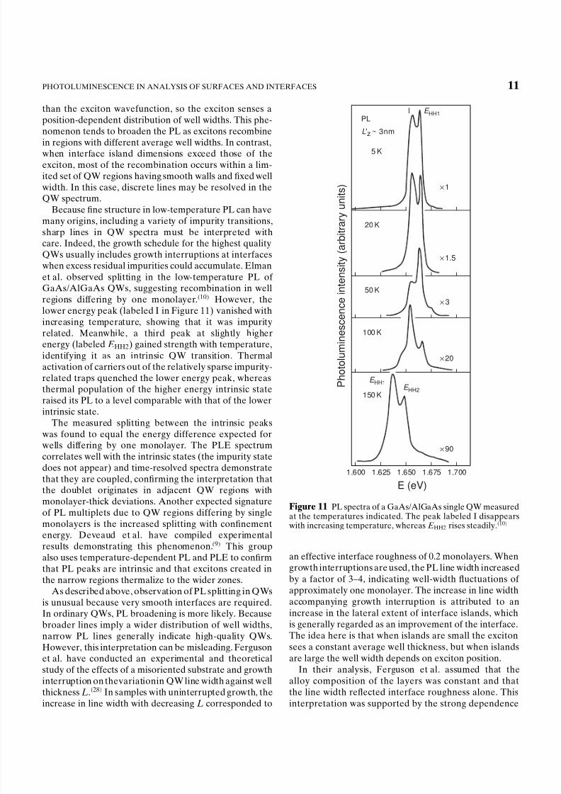
Because fine structure in low-temperature PL can havemany origins, including a variety of impurity transitions,sharp lines in QW spectra must be interpreted withcare. Indeed, the growth schedule for the highest qualityQWs usually includes growth interruptions at interfaceswhen excess residual impurities could accumulate. Elman
et al. observed splitting in the low-temperature PL of GaAs/AlGaAs QWs, suggesting recombination in wellregions differing by one monolayer.10 However, thelower energy peak (labeled I in Figure 11) vanished withincreasing temperature, showing that it was impurityrelated. Meanwhile, a third peak at slightly higherenergy (labeled EHH2) gained strength with temperature,identifying it as an intrinsic QW transition. Thermalactivation of carriers out of the relatively sparse impurity-related traps quenched the lower energy peak, whereasthermal population of the higher energy intrinsic stateraised its PL to a level comparable with that of the lowerintrinsic state.
The measured splitting between the intrinsic peakswas found to equal the energy difference expected forwells differing by one monolayer. The PLE spectrumcorrelates well with the intrinsic states (the impurity statedoes not appear) and time-resolved spectra demonstratethat they are coupled, confirming the interpretation thatthe doublet originates in adjacent QW regions withmonolayer-thick deviations. Another expected signatureof PL multiplets due to QW regions differing by singlemonolayers is the increased splitting with confinementenergy. Deveaud et al. have compiled experimentalresults demonstrating this phenomenon.9 This group
also uses temperature-dependent PL and PLE to confirmthat PL peaks are intrinsic and that excitons created inthe narrow regions thermalize to the wider zones.
As described above, observation of PL splitting in QWsis unusual because very smooth interfaces are required.In ordinary QWs, PL broadening is more likely. Becausebroader lines imply a wider distribution of well widths,narrow PL lines generally indicate high-quality QWs.However, this interpretation can be misleading. Fergusonet al. have conducted an experimental and theoreticalstudy of the effects of a misoriented substrate and growthinterruption on thevariationin QW line width against well
thickness L.28
In samples with uninterrupted growth, theincrease in line width with decreasing L corresponded to
PLI E HH1
E HH1E HH2
5 K
20 K
50 K
100 K
150 K
× 1
× 1.5
× 3
× 20
× 90
' ~ 3nmLz
1.600 1.625 1.650 1.675 1.700
E (eV)
P h o t o l u m i n e s c e n c e i n t e n s i t y ( a r b i t r a r y u n i t s )
Figure 11 PL spectra of a GaAs/AlGaAs single QW measuredat the temperatures indicated. The peak labeled I disappearswith increasing temperature, whereas EHH2 rises steadily.10
an effective interface roughness of 0.2 monolayers. Whengrowth interruptions are used, the PL line width increasedby a factor of 3–4, indicating well-width fluctuations of approximately one monolayer. The increase in line widthaccompanying growth interruption is attributed to anincrease in the lateral extent of interface islands, whichis generally regarded as an improvement of the interface.The idea here is that when islands are small the excitonsees a constant average well thickness, but when islandsare large the well width depends on exciton position.
In their analysis, Ferguson et al. assumed that thealloy composition of the layers was constant and that
the line width reflected interface roughness alone. Thisinterpretation was supported by the strong dependence

8/8/2019 Photo Luminescence of Surfaces and Interfaces
http://slidepdf.com/reader/full/photo-luminescence-of-surfaces-and-interfaces 14/25
12 SURFACES
0
0.8
1.6
10 20
L (nm)
f w h m
( m e V )
30
x = 0.09
T = 5 K
γ intγ
all
Figure 12 Experimental (dots) and theoretical (solid line) full
width at half-maximum (fwhm) of the exciton recombinationline in InGaAs/GaAs QWs. Interface roughness (gint, dottedline) and alloy disorder (gall, dashed line) contributions to thetheoretical result are shown separately.30
of line width on L. Woods et al. studied the PL of InGaAsP/InGaAsP QWs and came to the oppositeconclusion.29 Because the line width did not increasein the narrow wells, the broadening was attributed toalloy composition variation in the well and barrier layers.In general, of course, both mechanisms will contributeto the PL line width. For example, Patane et al. foundthat alloy disorder and interface roughness are requiredto fit the L dependence of In xGa1 xAs/GaAs PL lines.30
Although alloy disorder is sufficient to explain the linewidth in wide wells, interface roughness is necessary tofit the data at small L (see Figure 12). When x D 1, alloybroadening is absent and interface roughness alone mustaccount for the L-dependent line width.
4 PHOTOLUMINESCENCE INTENSITY
Of all the properties that characterize PL, the intensity
of the PL signal has received the most attention inthe analysis of interfaces. This interest is due to thefact that, although several important mechanisms affectthe PL response, it is generally found that large PLsignals correlate with good interface properties. A usefulreview of the dominant mechanisms and the relationshipbetween them has been provided by Chang et al.31
In particular, they discuss the roles of the surfacerecombination velocity S and band bending at the surfacein the PL measurement. Because surface recombinationis usually nonradiative, and band bending can lead to theformation of a depletion region or ‘‘dead layer’’ where PL
is effectively quenched, both of these phenomena tend toreduce the PL intensity. Distinguishing between the two
effects is difficult and usually requires a supplementarymeasurement of the surface potential.
All else being constant, the surface recombination
velocity is proportional to the density of surface states.However, changes in the surface-state density can affectthe accumulation of charge at the surface, thereby alteringthe depletion thickness. If increasing the surface-statedensity enhances the depletion layer, both mechanismssuppress the PL intensity and the surface recombinationvelocity increases rapidly. Conversely, if the space-chargeregion is reduced by an increase in the density of surfacestates, the two mechanisms will have opposite effectson the PL signal and tend to cancel each other out.It should also be noted that, even though changes insurface-state density usually affect band bending, the
inverse is not necessarily true. For example, the electricfield at the surface can be modified by adsorption of molecules that shift the distribution of electrons betweenbulk and surface states but leave the surface-state densityunchanged. Hence, the coupling of the two phenomena isquite complex.
PL intensity measurements have been used to evaluatea wide variety of surface treatments, including etching,oxidation, hydrogenation, adsorption of gases, depositionof coatings, and heteroepitaxy. The results are usuallyinterpreted within the context of one of the abovemodels: changes in surface-state density or changes indepletion thickness. Occasionally, when supplementarymeasurements of the surface Fermi level or dependenceon applied bias are performed, more sophisticated modelsthat account for both mechanisms are used. Otherwise,restricting the discussion to changes in an effective surfacerecombination velocity, which contains both effects, canaccommodate the ambiguity of the phenomena.
Because a strong PL response is widely regardedas an indicator of a high-quality surface, and PLmeasurements are nondestructive and environment-insensitive, PL intensity measurements are an importantin situ evaluation tool. The PL signal is monitored in realtime while the surface is physically or chemically modified.
Hence, the advantage of in situ methods is that processingsteps can be controlled and optimized precisely. Therelative ease of the experiment, combined with thebroad implications of results for the optoelectronicsindustry, has made in situ PL a very popular technique.Indeed, the method has been used to characterize thedevelopment of virtually every technologically importantsurface undergoing almost every technologically relevantprocess. In these experiments, it is important to bear inmind that PLE itself can induce or accelerate chemicalinteractions.32
As an example, in situ PL has been used to assess
InP surfaces during various cleaning and etching steps,oxidation, ambient gas flow, plasma exposure, and
8/8/2019 Photo Luminescence of Surfaces and Interfaces
http://slidepdf.com/reader/full/photo-luminescence-of-surfaces-and-interfaces 15/25
PHOTOLUMINESCENCE IN ANALYSIS OF SURFACES AND INTERFACES 13
heating.31,32 In some cases, laser-induced interactionswere found to alter etch rates, surface morphology, andsurface contamination.32 The results are explained bythe availability of photoexcited electrons and holes thatcatalyze chemical reactions. In situ PL has also been usedto probe the passivation of GaAs with heteroepitaxialAlGaAs monolayer by monolayer.33 Conducting asimilar study outside the growth chamber would haverequired a long sequence of separate growth runs,where run-to-run scatter in growth conditions could beproblematic. Timoshenko et al. have extended the in situPL technique to evaluate electrochemical treatments of indirect semiconductor surfaces, where pulsed excitationis required to obtain a sufficient PL signal.34
An interesting application of surface-adsorbate-in-
duced changes in PL intensity has been described in aseries of publications by Ellis et al.35 Molecular speciesadsorbed onto semiconductor surfaces can be dividedinto two categories: Lewis acids that have a large electronaffinity, and Lewis bases that have a small electron affinityrelative to the work function of the material. Lewis acidsdraw electrons from the bulk to surface electronic states,and Lewis bases push electrons from surface states intothe bulk. These shifts in surface charge expand or contractthe depletion thickness of the semiconductor, quenchingor enhancing the PL intensity. Hence, the partial pressureof a gaseous species that adsorbs to a semiconductor
surface can be inferred by monitoring the PL signal, thusforming the basis for a novel chemical sensor.
4.1 Dependence on Applied Bias: Surface Potential
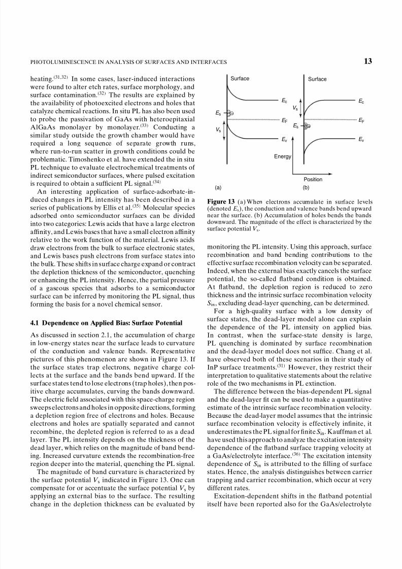
As discussed in section 2.1, the accumulation of chargein low-energy states near the surface leads to curvatureof the conduction and valence bands. Representativepictures of this phenomenon are shown in Figure 13. If the surface states trap electrons, negative charge col-lects at the surface and the bands bend upward. If thesurface states tend to lose electrons (trap holes), then pos-itive charge accumulates, curving the bands downward.
The electric field associated with this space-charge regionsweeps electrons and holes in opposite directions, forminga depletion region free of electrons and holes. Becauseelectrons and holes are spatially separated and cannotrecombine, the depleted region is referred to as a deadlayer. The PL intensity depends on the thickness of thedead layer, which relies on the magnitude of band bend-ing. Increased curvature extends the recombination-freeregion deeper into the material, quenching the PL signal.
The magnitude of band curvature is characterized bythe surface potential V s indicated in Figure 13. One cancompensate for or accentuate the surface potential V s by
applying an external bias to the surface. The resultingchange in the depletion thickness can be evaluated by
Surface
(a)
E s
V s
E F
Energy
Position
E c
E v
Surface
(b)
E s
V s
E F
E c
E v
−− −
+ ++
Figure 13 (a) When electrons accumulate in surface levels(denoted Es), the conduction and valence bands bend upwardnear the surface. (b) Accumulation of holes bends the bandsdownward. The magnitude of the effect is characterized by thesurface potential V s.
monitoring the PL intensity. Using this approach, surfacerecombination and band bending contributions to theeffective surface recombination velocity can be separated.Indeed, when the external bias exactly cancels the surfacepotential, the so-called flatband condition is obtained.At flatband, the depletion region is reduced to zerothickness and the intrinsic surface recombination velocitySin, excluding dead-layer quenching, can be determined.
For a high-quality surface with a low density of surface states, the dead-layer model alone can explainthe dependence of the PL intensity on applied bias.In contrast, when the surface-state density is large,PL quenching is dominated by surface recombinationand the dead-layer model does not suffice. Chang et al.have observed both of these scenarios in their study of InP surface treatments.31 However, they restrict theirinterpretation to qualitative statements about the relativerole of the two mechanisms in PL extinction.
The difference between the bias-dependent PL signal
and the dead-layer fit can be used to make a quantitativeestimate of the intrinsic surface recombination velocity.Because the dead-layer model assumes that the intrinsicsurface recombination velocity is effectively infinite, itunderestimates the PL signal for finite Sin. Kauffman et al.have used this approach to analyze the excitation intensitydependence of the flatband surface trapping velocity ata GaAs/electrolyte interface.36 The excitation intensitydependence of Sin is attributed to the filling of surfacestates. Hence, the analysis distinguishes between carriertrapping and carrier recombination, which occur at verydifferent rates.
Excitation-dependent shifts in the flatband potentialitself have been reported also for the GaAs/electrolyte

8/8/2019 Photo Luminescence of Surfaces and Interfaces
http://slidepdf.com/reader/full/photo-luminescence-of-surfaces-and-interfaces 16/25
14 SURFACES
700 nm
550 nm
500 nm
400 nm
–1.6 –1.40
100
200
–1.2
Potential (V
vs. Ag/AgCl)
P L I n t e n s i t y ( a . u . )
–1.0 –0.8 –0.6
Figure 14 PL signal at 870 nm vs. applied potential for anetched p-GaAs electrode in 1 M NaOH. Excitation wavelengthsare indicated in the plot. The hysteresis in the measurement isattributed to a fundamental change in the nature of the surfaceduring the potential sweep.5
interface. Charge and potential distributions at inter-faces can be altered dramatically by illumination. Onemanifestation of the flatband shift is hysteresis in the mea-surement of PL intensity versus applied bias.5 It appearsthat the nature of the surface itself changes under specific
biasing and illumination conditions, altering the flatbandpotential and the associated depletion layer thickness.This phenomenon leads to different bias-dependent PLsignals for positive and negative voltage sweeps, as shownin Figure 14.
Under high excitation, surface states are saturated andthe accumulation of photogenerated carriers near thesurface screens the space-charge field. In this case, adecrease in the PL efficiency reflects the presence of additional surface states. High excitation measurementshave been used in this context to study the formation of corrosion-induced surface states at a GaAs/electrolyteinterface.37 After exposure, the PL signal quencheswhen the applied bias exceeds a value of 1 V above theflatband potential. This result indicates that the appliedbias bends the bands and that the new surface statesbecome populated only when the minority carrier quasi-Fermi level reaches the energy of the states. Thus, fromthe dependence on applied bias, the energetic position of the new levels can be ascertained.
4.2 Spatial Dependence: Interface Uniformityand Carrier Diffusion
Because PL intensity is an indicator of interface quality,
measurements of the PL signal vs. position provide infor-mation on the spatial uniformity of interface properties.
The nondestructive and environment-insensitive featuresof PL make this application particularly useful in theevaluation of substrate surfaces, where detection of elec-
trically active features may help to control problemsin epitaxial devices. Such features might be overlookedin mechanical investigations of surface morphology.Although the spatial resolution in a PL scanning appli-cation is ultimately dictated by surface area and scantime, the diffraction limit of approximately 1 µm can beachieved in the best experimental arrangements. Thesehigh-resolution schemes must address carrier diffusion,which can smear images on a much larger scale.
Spatially resolved PL measurements are usually accom-plished by scanning the optical excitation spot relative tothe sample surface and detecting the PL signal in the far
field. One of the first demonstrations of this approachwas made by Krawczyk et al. in an investigation of InPsurface treatments.38 By coupling the excitation into oneend of an optical fiber and scanning the other end relativeto a focusing objective, they achieved resolution of theorder of a few microns. They observed wide variationin the PL signal on a microscopic scale. For example,PL images of the effect of annealing on NH4OH-treatedInP are shown in Figure 15. The PL topography evolvesfrom a random distribution of depressions and peaksto a flat response with randomly distributed PL islands.The annealing results are attributed to the presence of small oxide islands that protect the surface from thermaldegradation.
Scanning the excitation laser with stepping motors orgalvanometer mirrors usually requires a few seconds toaccumulate a PL image. However, high-speed rasteringwith resonant mirrors or acousto-optic devices cangenerate frames at standard video rates.39 In this case,PL images can be observed in real time. An additionaladvantage of video-rate laser scanning is the short dwelltime (less than 1 µs) at each excitation position, whichminimizes the possibility of photodegradation.
Although spatially resolved PL usually focuses on theband edge or integrated PL signal, spectral selectivity
can be incorporated to map the distribution of particularsurface states. Tajima has used this approach to plot thedeep-level distribution in the near-surface region of GaAsand Si wafers.40 Because these states tend to saturate athigh excitation, he emphasizes the importance of using alow laser power and stabilizing the system mechanicallyto accommodate long dwell times. He also points outthat the surface finish must be controlled carefully toavoid surface-treatment-related phenomena like thosediscussed above.
The spatial dependence of the PL spectrum itself can beused to evaluate uniformity of alloy composition, epilayer
thickness, and a variety of other material properties thataffect PL spectra. For example, the PL spectrum has

8/8/2019 Photo Luminescence of Surfaces and Interfaces
http://slidepdf.com/reader/full/photo-luminescence-of-surfaces-and-interfaces 17/25
PHOTOLUMINESCENCE IN ANALYSIS OF SURFACES AND INTERFACES 15
(a)
(b)
(c)
20 µm
Figure 15 PL images of InP treated with NH4OH: (a) astreated; (b) annealed at 350 °C; (c) annealed at 450 °C. ThePL intensity scale in (b) and (c) is 10 times smaller than in(a).38
been recorded as a function of position to look for signsof dislocations or residual stress in laterally overgrownInP on InP-coated Si substrates.41 Dislocations areexpected to reduce the PL signal, and stress tends toshift and broaden PL peaks. Hence, the spatially resolvedInP/Si PL was compared with that of lattice-matchedInP layers grown homoepitaxially on InP substrates. The
measured PL peak was as strong and narrow as that of the homoepitaxial InP with little shift in peak wavelength,suggesting that the overgrowth layer was dislocation andstress free. In addition, the PL spectrum was independentof position, indicating good uniformity in layer quality.
When a laser is focused on a surface, the minimumspot size is determined by the diffraction limit, whichis approximately equivalent to the wavelength of thelaser light. In the analysis of semiconductors, the opticalexcitation energy must exceed the bandgap, which usuallycorresponds to wavelengths in the visible or near-infrared. Hence, the diffraction-limited spot size is of
the order of 1 µm. In the absence of carrier diffusion,the excitation spot size governs the spatial resolution
of PL measurements. However, photogenerated carriersoften diffuse average distances much larger than 1 µmbefore recombining, so the PL is generated in a broader
region than the original excitation spot. Restricting thePL collection can circumvent diffusion-limited spatialresolution.
The most straightforward approach to this problem isa PL extension of confocal microscopy. Using matchedillumination and collection optics with back focal planeapertures, enhanced spatial resolution, improved depthprofiling, and insensitivity to scattered light are obtained.Only light originating in the focal spot is imaged by thecollection optics. In the context of PL experiments, theconfiguration rejects luminescence due to recombinationof carriers outside the illuminated area. A typical
experimental set-up is shown in Figure 16. Fong et al.have used confocal PL to study a GaAs/AlGaAs QWgrown on a grooved substrate.42 The improved spatialresolution permitted them to profile abrupt fluctuations(on a scale of 1 µm) in alloy composition and QWthickness. In the confocal measurement, if the detection
To photo detector
Aperture
Aperture
PumpbeamBeam-
splitter
Lens
Sample
Figure 16 Typical experimental set-up for confocal PL mea-surements.
8/8/2019 Photo Luminescence of Surfaces and Interfaces
http://slidepdf.com/reader/full/photo-luminescence-of-surfaces-and-interfaces 18/25
16 SURFACES
aperture is translated laterally in the image plane, thecorresponding detection spot can be maneuvered relativeto the excitation spot. This technique can be used
to monitor the diffusion process itself. For example,Hubner et al. have measured the diffusion length alongsemiconductor quantum wire structures.43 A variation incarrier transport with wire width is explained by changesin sidewall recombination due to different surface-to-volume ratios.
Finally, it should be pointed out that the diffractionlimit itself canbe surmounted when optical measurementsare made in the near-field. If a subwavelength apertureis positioned in the near-field region of the opticalemission, resolution comparable to the aperture size canbe obtained. The most straightforward manifestation of
this idea is to place a mask with a tiny hole very closeto the sample surface such that excitation and PL mustpass through the aperture. A more popular techniqueknown as near-field scanning optical microscopy utilizesthe tip of an extruded optical fiber to excite and/orcollect the PL emission. Both of these approaches haveproduced spatial resolution of the order of 100 nm. Yet,with emission areas this small, generating sufficient PLsignal under appropriate excitation conditions can bequite challenging.
4.3 Time Dependence: Recombination Rates
When CW excitation is used in a PL experiment, thesystem quickly converges on steady state. The rate of excitation equals the rate of recombination, and thephotogenerated carrier density is constant in time. Incontrast, when a material is excited by a series of short laser pulses, the concentration of carriers dependsstrongly on time. Because the laser pulse can be muchshorter than the average recombination time, a specificcarrier density can be generated almost instantaneously.The photoexcited carriers then recombine at a ratethat is characteristic of the recombination path theyfollow. Time-resolved PL measurements can be used
to determine carrier lifetimes, and to identify andcharacterize various recombination mechanisms in thematerial.
Photogenerated carrier lifetimes are obtained bymonitoring the transient PL signal after pulsed excitation.Although the experimental apparatus required to makesuch a measurement depends on the desired resolution,the most common detection scheme is time-correlatedsingle photon counting. When a photon is incident on aphotodetector, an electrical pulse is generated. This pulseand an excitation reference pulse are fed into a constantfraction discriminator, which is designed to create output
pulses that are timed correctly independent of input pulsesize. Next, the signal and reference pulses are sent to
a time-to-amplitude converter. This device uses the twoinput pulses as start and stoptriggers for a linearly chargedtiming capacitor and produces an output pulse whose
amplitude is governed by the capacitor charge. Thus, theoutput pulse height is proportional to the delay betweeninput pulses. The output pulses are sorted accordingto amplitude and counted by a multichannel analyzer,yielding the transient PL decay.
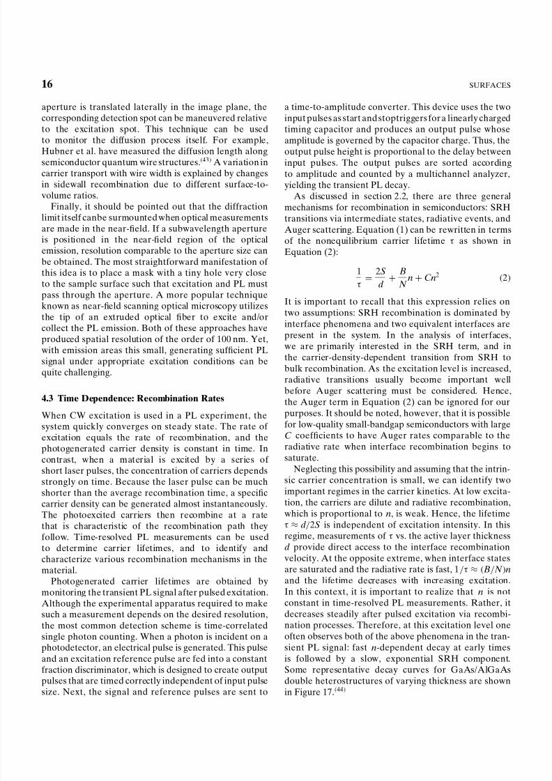
As discussed in section 2.2, there are three generalmechanisms for recombination in semiconductors: SRHtransitions via intermediate states, radiative events, andAuger scattering. Equation (1) can be rewritten in termsof the nonequilibrium carrier lifetime t as shown inEquation (2):
1tD 2S
dC B
N nCCn2 2
It is important to recall that this expression relies ontwo assumptions: SRH recombination is dominated byinterface phenomena and two equivalent interfaces arepresent in the system. In the analysis of interfaces,we are primarily interested in the SRH term, and inthe carrier-density-dependent transition from SRH tobulk recombination. As the excitation level is increased,radiative transitions usually become important wellbefore Auger scattering must be considered. Hence,the Auger term in Equation (2) can be ignored for our
purposes. It should be noted, however, that it is possiblefor low-quality small-bandgap semiconductors with largeC coefficients to have Auger rates comparable to theradiative rate when interface recombination begins tosaturate.
Neglecting this possibility and assuming that the intrin-sic carrier concentration is small, we can identify twoimportant regimes in the carrier kinetics. At low excita-tion, the carriers are dilute and radiative recombination,which is proportional to n, is weak. Hence, the lifetimet ³ d/2S is independent of excitation intensity. In thisregime, measurements of t vs. the active layer thickness
d provide direct access to the interface recombinationvelocity. At the opposite extreme, when interface statesare saturated and the radiative rate is fast, 1/t ³ B/N n
and the lifetime decreases with increasing excitation.In this context, it is important to realize that n is notconstant in time-resolved PL measurements. Rather, itdecreases steadily after pulsed excitation via recombi-nation processes. Therefore, at this excitation level oneoften observes both of the above phenomena in the tran-sient PL signal: fast n-dependent decay at early timesis followed by a slow, exponential SRH component.Some representative decay curves for GaAs/AlGaAs
double heterostructures of varying thickness are shownin Figure 17.44

8/8/2019 Photo Luminescence of Surfaces and Interfaces
http://slidepdf.com/reader/full/photo-luminescence-of-surfaces-and-interfaces 19/25
PHOTOLUMINESCENCE IN ANALYSIS OF SURFACES AND INTERFACES 17
0
n+ /n− /n+
10.0 µm
804 ns
0.3 µm
213 ns
GaAs/AI0.3Ga0.7As
1.0 µm
827 ns
GaAs/AI0.3Ga0.7As
9.82 µm
2.5 us
GaAs/AI0.3Ga0.7As
2 4 6 8100
103
106
109
1012
Time (µs)
P L I n t e n s i t y
Figure 17 PL decay curves for a set of GaAs/AlGaAs doubleheterostructures and an nC/n/nC GaAs homostructure. Active
layer thickness (µm) and carrier lifetime (ns) are indicated inthe plot (lifetimes are obtained by fitting the exponential tail of the curves).44
Quantitative analysis of such nonexponential multi-component decay curves is difficult. The situation issimplified in the case of doped materials with rel-atively high equilibrium carrier concentrations. Here,the photoexcitation can be kept well below the dop-ing level so that the fixed majority carrier densitycontrols the recombination kinetics. Because n is essen-tially constant throughout the transient measurement,
the lifetime is independent of excitation even in theradiative and Auger regimes. Lifetimes in a set of sam-ples covering a wide range of doping concentrations canyield accurate recombination coefficients.45 In partic-ular, a discrete transition from n-independent lifetimesto steadily decreasing n-dependent lifetimes should beobserved when the carrier concentration reaches thethreshold for significant bulk contributions.
Returning to the intrinsic (low equilibrium carrierconcentration) case, if the pulsed excitation is keptsufficiently weak then even the initial photoexcited carrierdensity is within theSRH regime. Thus, an exponential PL
decay with a constant lifetime is expected. As describedabove, the variation in t with layer thickness yields
100 40 2020
10
0 10 20 30 40 50 60
d –1 (× 104 cm –1)
N zn: 3.5 × 1017 cm –3
N zn: 2.5 × 1017 cm –3
Undoped
d z2
d z1
τ – 1 ( ×
1 0 7 s
– 1 )
Ι ΙΙ ΙΙΙ
(nm)
Figure 18 Recombination rate vs. the reciprocal of the activelayer thickness in Zn-doped AlGaInP/GaInP double het-erostructures. Symbols representing different doping levels arespecified in the plot.46
the interface recombination velocity S. An excellentexample of this type of experiment is the investigationby Domen et al. of Zn doping in AlGaInP/GaInP doubleheterostructures.46 Zinc was intentionally incorporatedinto the upper cladding layer and the resulting carrierlifetime in the active layer was evaluated via time-resolved PL. Measured lifetimes for different dopingconcentrations are plotted against active layer thicknessin Figure 18. The results show the expected behavior1/t / 1/d when separated into three regimes that aredistinguished by the size of the active layer relative to theZn-diffused region. In region I, only the top interface isdegraded by thepresence of Zn. In region II,an increasingfraction of the active layer suffers from diffused Zn. Inregion III, the high-concentration Zn penetrates all theway through the thin active layer and attacks the bottomcladding interface. The recombination velocities at therelevant interfaces are quickly obtained from the slope of
the linear fits.Time-resolved PL can also be used to distinguish
between surface-state and depletion-layer contributionsto PL quenching. A decrease in the integrated PL sig-nal implies that the nonradiative recombination rate isenhanced relative to the radiative rate. Such an enhance-ment can be attributed to one of two mechanisms: anincrease in the density of interface states, or an increase inthe dead layer thickness. In transient PL, accelerated non-radiative recombination is manifested as a decrease in thephotoexcited carrier lifetime. For example, wet-etch sur-face modification of GaInP has been characterized by CW
and time-resolved PL.47
Etchants yielding enhanced CWPL signals produced corresponding increases in carrier

8/8/2019 Photo Luminescence of Surfaces and Interfaces
http://slidepdf.com/reader/full/photo-luminescence-of-surfaces-and-interfaces 20/25
18 SURFACES
lifetime, indicating that the nonradiative recombinationrate is effectively reduced.
In this particular experiment, it is not clear whether
the etching procedure removes nonradiative recombi-nation sites or depletion-inducing surface charge. Thisshortcoming in the interpretation can be addressed byconducting the transient PL measurements at high exci-tation, where photoexcited carriers screen the electricfield in the space-charge region. If the injection levelis sufficiently high, the bands are essentially flat atthe surface and changes in the carrier lifetime can beunambiguously attributed to changes in the surface-statedensity. Lunt et al. have demonstrated this approach in acomprehensive investigation of GaAs surfaces exposed toa variety of sulfur, nitrogen, and oxygen donors.48 Some
treatments produced an increase in the flatband carrierlifetime, indicating a decrease in the intrinsic surfacerecombination velocity. Meanwhile, other reagents pro-duced substantial increases in the steady-state PL signalbut did not affect the high-injection recombination rate.In this case, the results suggest that the enhanced PL isprimarily due to changes in the equilibrium band bending.Thus, the two phenomena are effectively separated.
One final application of transient PL to note isthe identification of transitions involving type II bandalignment. Because these transitions occur betweenelectrons and holes that are separated in real space
(see Figure 6), the electron–hole wavefunction overlapis small. Thus, type II optical transitions are expected toproceed more slowly than transitions in type I systems.19
4.4 Temperature Dependence: Thermal Population
When light is incident on a semiconductor, photoexcita-tion of electrons from the valence to conduction bandcan occur for any photon energy exceeding the bandgap.In this process, the difference between the excitationenergy and the bandgap goes into the kinetic energy of the photoexcited carriers. Thus, the initial distribution of electron and hole energies depends on energy conserva-
tion, not temperature, and the original carrier populationsare nonthermal. For example, if the excitation energy ismuch larger than the bandgap, the electrons and holeswill be created high in their respective bands with kineticenergies far exceeding the characteristic thermal energyof the lattice kT . The electrons and holes then thermalizewith the lattice by emitting phonons and, in the absenceof Fermi filling effects, settle into Boltzmann distributionsabove their respective band edges. Because this processalmost always occurs on a timescale much faster thanthat of recombination, thermal distributions are usuallyobserved in ordinary PL. Thus, in PL experiments, tem-
perature is primarily used to tune the thermal occupationof available states.
At the lowest temperatures, PL is dominated by thelowest energy levels. For instance, excitons (electronsand holes bound by the Coulomb interaction) and
shallow impurity traps often appear in low-temperaturePL. These states are characterized by binding energiesof the order of a few milli-electron-volts, which issmall relative to kT at ordinary temperatures. As thesample temperature and corresponding thermal energyare increased, excitons dissociate and carriers vacateshallow traps, reducing the intensity of these featuresin the PL spectrum. It is important to note here that thePL signal from any level depends on two parameters:the fractional population, and the density of participatingstates. Thus, relatively sparse low-energy traps appearin low-temperature PL because the thermal population
of high-density band levels is very small. However, whenthe thermal population of band levels is appreciable, bandtransitions dominate the PL because of the abundance of states taking part.
In addition to the population of discrete states, thermaldistributions are manifested in the PL line width of band-edge transitions. When kT exceeds the inhomogeneousbroadening in the sample, a high-energy Boltzmann tailappears on the PL peak. This feature can be usefulfor estimating the local temperature of the sample.However, because thermal quenching can hide sparselow-energy states and thermal broadening can obscureimportant details in the spectrum, certain PL experimentsmust be conducted at relatively low (i.e. liquid helium)temperatures.
Relative changes in state population with temperatureprovide evidence that PL peaks originate in the samepart of the sample and that carriers are free tomove between the available states. As discussed insection 3.2, multiple peaks in the PL of high-qualityQWs are frequently attributed to states in regionsof the well differing by single monolayers. In thesesystems, thermal redistribution among states rules outan important competing explanation: the peaks being dueto recombination in separate regions of the sample where
carriers do not mix. The temperature-dependent PLspectra in Figure 11 clearly show thermal redistributionamong states. The peak labeled EHH2 gains strengthwith increasing temperature, as expected for thermalpopulation of a higher energy state. In contrast, the peaklabeled I vanishes at high temperature, demonstratingthe importance of the other parameter that controls PLintensity – the density of states. Peak I is strong at lowtemperature because carriers are trapped at these sitesand do not have enough thermal energy to escape, butit disappears at high temperature because the states aresparse relative to the intrinsic bands.
In the characterization of discrete low-energy states,quantitative analysis of the decrease in PL intensity with
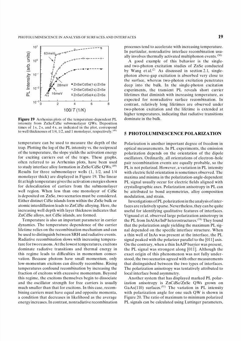
8/8/2019 Photo Luminescence of Surfaces and Interfaces
http://slidepdf.com/reader/full/photo-luminescence-of-surfaces-and-interfaces 21/25
PHOTOLUMINESCENCE IN ANALYSIS OF SURFACES AND INTERFACES 19
10 –3
10 –2
10 –1
100
101
0 2 4 6 8
63meV
28meV
16meV
ZnSe/CdSe(1 s)/ZnSe
ZnSe/CdSe(2 s)/ZnSe
ZnSe/CdSe(4 s)/ZnSe P L I n t e n s i t y ( a r b . u n i t s )
100/ T (1/K)
Figure 19 Arrhenius plots of the temperature-dependent PLintensity from ZnSe/CdSe submonolayer QWs. Depositiontimes of 1 s, 2 s, and 4 s, as indicated in the plot, correspondto well thicknesses of 1/4, 1/2, and 1 monolayer, respectively. 49
temperature can be used to measure the depth of thetrap. Plotting the log of the PL intensity vs. the reciprocalof the temperature, the slope yields the activation energyfor exciting carriers out of the traps. These graphs,often referred to as Arrhenius plots, have been usedto study interface alloy formation in ZnSe/CdSe QWs.49
Results for three submonolayer wells (1, 1/2, and 1/4monolayer thick) are displayed in Figure 19. The linearfit at high temperature gives the activation energies shownfor delocalization of carriers from the submonolayerwell region. When less than one monolayer of CdSeis deposited on ZnSe, two scenarios must be considered.Either distinct CdSe islands form within the ZnSe bulk oratomic interdiffusion leads to ZnCdSe alloying. Here, theincreasing well depth with layer thickness indicates thatZnCdSe alloys, not CdSe islands, are formed.
Temperature is also an important parameter in carrierdynamics. The temperature dependence of the carrierlifetime relies on the recombination mechanism and canbe used to distinguish between SRH and radiative events.
Radiative recombination slows with increasing tempera-ture for two reasons. At the lowest temperatures, excitonsdominate radiative transitions and thermal energy inthis regime leads to difficulties in momentum conser-vation. Because photons have small momentum, onlylow-momentum excitons can directly recombine. Risingtemperatures confound recombination by increasing thefraction of excitons with excessive momentum. Beyondthis regime, the excitons themselves begin to dissociateand the oscillator strength for free carriers is usuallymuch smaller than that for excitons. In this case, recom-bining carriers must have equal and opposite momenta,
a condition that decreases in likelihood as the averageenergy increases. In contrast, nonradiative recombination
processes tend to accelerate with increasing temperature.In particular, nonradiative interface recombination usu-ally involves thermally activated multiphonon events.50
A good example of this behavior is the single-and two-photon excitation studies of ZnSe conductedby Wang et al.2 As discussed in section 2.1, single-photon above-gap excitation is absorbed very close tothe surface, whereas two-photon excitation penetratesdeep into the bulk. In the single-photon excitationexperiments, the transient PL reveals short carrierlifetimes that diminish with increasing temperature, asexpected for nonradiative surface recombination. Incontrast, relatively long lifetimes are observed undertwo-photon excitation and the lifetime is extended athigher temperatures, indicating that radiative transitions
dominate in the bulk.
5 PHOTOLUMINESCENCE POLARIZATION
Polarization is another important degree of freedom inoptical measurements. In PL experiments, the emissionpolarization depends on the orientation of the dipoleoscillators. Ordinarily, all orientations of electron–holepair recombination events are equally probable, so thePL is not polarized. However, a variation in PL intensitywith electric field orientation is sometimes observed. The
maxima and minima in the polarization-angle-dependentPL signal usually occur for electric fields aligned withcrystallographic axes. Polarization anisotropy in PL canbe attributed to bond asymmetries, alloy compositionmodulation, and strain.
Investigations of PL polarization in the analysis of inter-faces are relatively sparse. Nevertheless, they can be quiteuseful for identifying qualitative features of interfaces.Vignaud et al. observed large polarization anisotropy inthe PL from InAlAs/InP heterostructures.19 They foundthat the polarization angle yielding the maximum PL sig-nal depended on the specific interface structure. Whena thin well of InAs was present at the interface, the PL
signal peaked with the polarizer parallel to the [011] axis.On the contrary, when a thin InAlP barrier was present,the PL signal was strongest along [01 N1]. Although theexact origin of this phenomenon was not fully under-stood, the two scenarios agreed with other measurementsthat distinguished between the two types of interfaces.The polarization anisotropy was tentatively attributed tolocal interface bond asymmetry.
Another system that has displayed marked PL polar-ization anisotropy is ZnCdSe/ZnSe QWs grown onGaAs(110) surfaces.51 The variation in PL intensitywith polarization angle for one such QW is shown in
Figure 20. The ratio of maximum to minimum polarizedPL signals can be calculated using Luttinger parameters,

8/8/2019 Photo Luminescence of Surfaces and Interfaces
http://slidepdf.com/reader/full/photo-luminescence-of-surfaces-and-interfaces 22/25
20 SURFACES
0 90 180 270 360
(001)
SQW
Polarization angle α (deg.)
I n t e n s i t y ( a r b . u n i t s )
(110)
[001]
[110][110] α
Figure 20 Polarization angle dependence of the PL intensityfrom a (110)-oriented ZnCdSe/ZnSe single QW. The solid lineis a simple sinusoidal fit.51
which describe the valence band dispersion in thesemiconductor. Assuming that the Luttinger parametersof ZnCdSe are similar to those of ZnSe, the calculatedratio is much smaller than that found experimentally.The enhanced polarization anisotropy in this system isattributed to compressive strain in the well layer. This
interpretation is consistent with the observation of a verynarrow PL line width in this sample. Because the latticemismatch is accommodated by uniform strain rather thandislocations at the interface, the distribution of states inthe QW should be relatively sharp.
6 CONCLUSION
PL analysis is a powerful tool in the characteriza-tion of surfaces and interfaces. Although a number of experimental techniques can provide detailed mechan-
ical information about interfaces, the optoelectronicsindustry that drives most interface investigations is ulti-mately concerned with optical and electronic properties.Mechanical information is useful because it is closelycorrelated with these properties, but PL measurementsexplore electronic features directly. Other techniques canprovide similar access, but they typically require moresophisticated excitation or detection schemes.
PLE is simple, but it is also quite versatile. The exci-tation energy and optical intensity can be chosen tostudy different regions and recombination mechanismsnear interfaces. Because absorption of the incident light
depends on the excitation energy, this parameter deter-mines the depth of the PL probe. Using PLE, absorption
and emission energies are observed simultaneously toevaluate the distribution of electronic states. The exci-tation intensity is even more important, controlling the
density of photoexcited electrons. This density is criticalin the interpretation of recombination dynamics.
The PL signal itself is characterized by three essentialfeatures: energy, intensity, and polarization. Because PLis the result of optical transitions between electronicstates, the PL spectrum gives precise information onthe energy levels available to electrons in the material.The intensity of the PL signal depends on the rate of radiative and nonradiative events, which depends in turnon the density of nonradiative interface states. Althoughinvestigations of PL polarization are still relatively sparseand are not well understood, they can identify unique
anisotropic features in the underlying crystal. Future workin this area should lead to a more complete picture of asymmetry at surfaces and interfaces.
PL measurements are not sensitive to the pressure inthe sample chamber and can be performed at virtuallyany temperature. These features make PL an excellentin situ probe of surface or interface modification. Evenso, variation of the PL signal with external parameterssuch as temperature and applied bias can provideadditional information on the nature of interfaces.Temperature-dependent thermal activation of electronicstates can be used to estimate their depth below theintrinsic bands. An applied bias shifts the bands at thesurface, permitting evaluation of the zero-bias bandbending. Thus, the availability of PL under a widevariety of experimental conditions provides for advancedmeasurement opportunities.
Applications of PL analysis range from simple spatialscans of epitaxial wafers to exhaustive investigationsof excitation-intensity-dependent PL in novel materials.Furthermore, new PL techniques continue to emerge,expanding the arsenal of PL analysis. Because PLE isusually absorbed near the surface, and interfaces tendto dominate electronic behavior in layered systems,PL is especially well suited to surface and interface
investigations. Interfaces are increasingly important innew optoelectronic materials where layered structures arebecoming thinner and more complex. Thus, although PLmeasurements have been useful for the characterizationand refinement of such materials, they can be expected toplay an even greater role in the future.
ABBREVIATIONS AND ACRONYMS
PL PhotoluminescencePLE Photoluminescence Excitation
PLS3
Photoluminescence Surface-stateSpectroscopy

8/8/2019 Photo Luminescence of Surfaces and Interfaces
http://slidepdf.com/reader/full/photo-luminescence-of-surfaces-and-interfaces 23/25
PHOTOLUMINESCENCE IN ANALYSIS OF SURFACES AND INTERFACES 21
QW Quantum WellRIE Reactive Ion EtchingSRA Spreading Resistance Analysis
SRH Shockley–Read–Hall
RELATED ARTICLES
Electronic Absorption and Luminescence (Volume 12)Surface Measurements using Absorption/Luminescence
REFERENCES
1. J. Garcia-Garcia, J. Gonzalez-Hernandez, J.G. Mendoza-
Alvarez, E.L. Cruz, G. Contreras-Puente, ‘Photolumi-
nescence Characterization of the Surface Layer of
Chemically Etched CdTe’, J. Appl. Phys., 67, 3810–3814
(1990).
2. H. Wang, K.S. Wong, B.A. Foreman, Z.Y. Yang, G.K.L.
Wong, ‘One- and Two-photon-excited Time-resolved
Photoluminescence Investigations of Bulk and Surface
Recombination Dynamics in ZnSe’, J. Appl. Phys., 83,
4773–4776 (1998).
3. R.E. Hollingsworth, J.R. Sites, ‘Photoluminescence Dead
Layer in p-Type InP’, J. Appl. Phys., 53, 5357– 5358
(1982).
4. H. Van Ryswyk, Arthur B. Ellis, ‘Optical Coupling
of Surface Chemistry. Photoluminescent Properties of
a Derivatized Gallium Arsenide Surface Undergoing
Redox Chemistry’, J. Am. Chem. Soc., 108, 2454– 2455
(1986).
5. K. Uosaki, Y. Shigematsu, S. Kaneko, H. Kita, ‘Photolu-
minescence and Impedance Study of p-GaAs/Electrolyte
Interfaces Under Cathodic Bias: Evidence for Flat-band
Potential Shift During Illumination and Introduction of
High-density Surface States by Pt Treatment’, J. Phys.
Chem., 93, 6521–6526 (1989).
6. K. Mettler, ‘Photoluminescence as a Tool for the Study of
the Electronic Surface Properties of GaAs’, Appl. Phys.,12, 75 – 82 (1977).
7. Y. Zhu, C. Ding, G. Ma, Z. Du, ‘Electronic State Char-
acterization of TiO2 Ultrafine Particles by Lumines-
cence Spectroscopy’, J. Solid State Chem., 139, 124–127
(1998).
8. M. Anpo, M. Kondo, S. Coluccia, C. Louis, M. Che,
‘Application of Dynamic Photoluminescence to the Study
of Active Surface Sites on Supported Mo/SiO2 Catalysts.
Features of Anchored and Impregnated Catalysts’, J. Am.
Chem. Soc., 111, 8791–8799 (1989).
9. B. Deveaud, A. Regreny, J.-Y. Emery, A. Chomette,
‘Photoluminescence Study of Interface Defects in High-
quality GaAs–GaAlAs Superlattices’, J. Appl. Phys., 59,1633–1640 (1986).
10. B.S. Elman, E.S. Koteles, C. Jagannath, Y.J. Chen,
S. Charbonneau, M.L.W. Thewalt, ‘Optical Character-
ization of Single Quantum Wells Fabricated Under
Conditions of Interrupted Growth’, Proc. SPIE, 794,44– 49 (1987).
11. J.M. Olson, R.K. Ahrenkiel, D.J. Dunlavy, B. Keyes,
A.E. Kibbler, ‘Ultralow Recombination Velocity at
Ga0.5In0.5P/GaAs Heterointerfaces’, Appl. Phys. Lett., 55,
1208–1210 (1989).
12. S. Komiya, A. Yamaguchi, I. Umebu, ‘Characterization
of Radiative Efficiency in Double Heterostructures of
InGaAsP/InP by Photoluminescence Intensity Analysis’,
Solid State Electron, 29, 235–240 (1986).
13. M. Mullenborn, N.M. Haegel, ‘Recombination Model for
Heterostructure Interfaces’, J. Appl. Phys., 74, 5748– 5753
(1993).
14. T.H. Gfroerer, E.A. Cornell, M.W. Wanlass, ‘Efficient
Directional Spontaneous Emission from an InGaAs/InP
Heterostructure with an Integral Parabolic Reflector’, J.
Appl. Phys., 84, 5360–5362 (1998).
15. T. Saitoh, H. Iwadate, H. Hasegawa, ‘InSituSurface State
Spectroscopy by Photoluminescence and Surface Current
Transport for Compound Semiconductors’, Jpn. J. Appl.
Phys., 30, 3750–3754 (1991).
16. T. Yoshida, T. Hashizume, H. Hasegawa, ‘Characteri-
zation of Interface Electronic Properties of Low-
temperature Ultrathin Oxides and Oxynitrides Formed
on Si(111) Surfaces by Contactless Capacitance–Voltage
and Photoluminescence Methods’, Jpn. J. Appl. Phys., 36,
1453–1459 (1997).
17. Y.J. Ding, C.L. Guo, J.B. Khurgin, K.-K. Law, J.L. Merz,
‘Characterization of Recombination Processes in Mul-
tiple Narrow Asymmetric Coupled Quantum Wells
Based on the Dependence of the Photoluminescence
on Laser Intensity’, Appl. Phys. Lett., 60, 2051–2053
(1992).
18. Y.J. Ding, D.C. Reynolds, S.J. Lee, J.B. Khurgin, W.S.
Rabinovich, D.S. Katzer, ‘Evidence for Strong Spatially
Localized Band-filling Effects at Interface Islands’, Appl.
Phys. Lett., 71, 2581–2583 (1997).
19. D. Vignaud, X. Wallart, F. Mollot, B. Sermage, ‘Photolu-
minescence Study of the Interface in Type II InAlAs–InP Heterostructures’, J. Appl. Phys., 84, 2138– 2145
(1998).
20. M.L.W. Thewalt, A.G. Steele, J.E. Huffman, ‘Photolumi-
nescence Studies of Ultrahigh-purity Epitaxial Silicon’,
Appl. Phys. Lett., 49, 1444–1446 (1986).
21. K.Akimoto, K.Tamamura, J. Ogawa, Y.Mori, C.Kojima,
‘Photoluminescence Study of the Interface of a GaAs/
Al xGa1 xAs Heterostructure Grown by Metalorganic
Chemical Vapor Deposition’, J. Appl. Phys., 63, 460– 464
(1988).
22. A. Henry, B. Monemar, J.L. Lindstrom, T.D. Bestwick,
G.S. Oehrlein, ‘Photoluminescence Characterization of
Plasma Exposed Silicon Surfaces’, J. Appl. Phys., 70,5597–5603 (1991).

8/8/2019 Photo Luminescence of Surfaces and Interfaces
http://slidepdf.com/reader/full/photo-luminescence-of-surfaces-and-interfaces 24/25
22 SURFACES
23. M.A. Foad, M. Watt, A.P. Smart, C.M. Sotomayor Tor-
res, C.D.W. Wilkinson, W. Kuhn, H.P. Wagner, S. Bauer,
H. Leiderer, W. Gebhardt, ‘High-resolution Dry Etching
of Zinc Telluride: Characterization of Etched Surfacesby X-ray Photoelectron Spectroscopy, Photolumines-
cence and Raman Scattering’, Semicond. Sci. Technol.,
6, A115–A122 (1991).
24. M.J. Joyce, M. Gal, J. Tann, ‘Observation of Interface
Defects in Strained InGaAs– GaAs by Photolumines-
cence Spectroscopy’, J. Appl. Phys., 65, 1377–1379
(1989).
25. L. Xu, X. Huang, H. Huang, H. Chen, J. Xu, K. Chen,
‘Surface Modificationand Enhancementof Luminescence
due to Quantum Effects in Coated CdSe/CuSe Semicon-
ductor Nanocrystals’, Jpn. J. Appl. Phys., 37, 3491–3494
(1998).
26. F.E.G. Guimaraes, B. Elsner, R. Westphalen, B. Span-
genberg, H.J. Geelen, P. Balk, K. Heime, ‘LP-MOVPE
Growth and Optical Characterization of GaInP/GaAs
Heterostructures: Interfaces, Quantum Wells, and Quan-
tum Wires’, J. Cryst. Growth, 124, 199–206 (1992).
27. M. Mesrine, J. Massies, E. Vanelle, N. Grandjean,
C. Deparis, ‘Photoluminescence Energy and Interface
Chemistry of GaInP/GaAs Quantum Wells’, Appl. Phys.
Lett., 71, 3552–3554 (1997).
28. I.T. Ferguson, C.M.S. Torres, T.M. Kerr, ‘The Optical
Properties of Thin Al0.3Ga0.7As–GaAs Quantum Wells
on Misoriented Substrates with [110] Terraces. A Study
of Interface Roughness Using Photoluminescence’, Semi-
cond. Sci. Technol., 7, 892–899 (1992).
29. L.M. Woods, P. Silvestre, P. Thiagarajan, G.A. Patrizi,
G.Y. Robinson, K.M. Jones, M. Al-Jassim, ‘Photolumi-
nescence and Interface Abruptness in InGaAsP/InGaAsP
Quantum Wells’, J. Electron.Mater , 23,1229–1233(1994).
30. A. Patane, A. Polimeni, M. Capizzi, F. Martelli, ‘Line-
width Analysis of the Photoluminescence of In xGa1 xAs/
GaAs Quantum Wells ( x D 0.09, 0.18, 1.0)’, Phys. Rev. B,
52, 2784–2788 (1995).
31. R.R. Chang, R. Iyer, D.L. Lile, ‘Surface Characterization
of InP Using Photoluminescence’, J. Appl. Phys., 61,
1995–2004 (1987).
32. H.J. Frenck, W. Kulisch, R. Kassing, ‘Characterization of InP Surfaces UsingIntegral Photoluminescence Measure-
ments’, Proc. SPIE , 1144, 250–258 (1989).
33. C.J. Sandroff, F.S. Turco-Sandroff, L.T. Florez, J.P. Har-
bison, ‘Recombination at GaAs Surfaces and GaAs/
AlGaAs Interfaces Probed by In Situ Photolumines-
cence’, J. Appl. Phys., 70, 3632–3635 (1991).
34. V.Yu. Timoshenko, J. Rappich, Th. Dittrich, ‘Express
Characterization of Indirect Semiconductor Surfaces
by In Situ Photoluminescence During Chemical and
Electrochemical Treatments’, Appl. Surf. Sci., 123/124,
111–114 (1998).
35. E.J. Winder, D.E. Moore, D.R. Neu, A.B. Ellis, J.F.
Geisz, T.F. Kuech, ‘Detection of Ammonia, Phosphine,and Arsine Gases by Reversible Modulation of Cadmium
Selenide Photoluminescence Intensity’, J. Cryst. Growth,
148, 63 – 69 (1995), and references therein.
36. J.F. Kauffman, C.S. Liu, M.W. Karl, ‘Surface Recombi-
nation Kinetics at the GaAs/Electrolyte Interface viaPhotoluminescence Efficiency Measurements’, J. Phys.
Chem. B, 102, 6766–6773 (1998).
37. B.A. Balko, G.L. Richmond, ‘Corrosion-induced Surface
States on n-GaAs as Studied by Photoluminescence
Versus Voltage Scans and Luminescence Decays’, J. Phys.
Chem., 97, 9002–9008 (1993).
38. S.K. Krawczyk, M. Garrigues, H. Bouredoucen, ‘Study of
InP Surface Treatments by Scanning Photoluminescence
Microscopy’, J. Appl. Phys., 60, 392–395 (1986).
39. G.E. Carver, ‘Scanned Photoluminescence with High
Spatial Resolution in Semi-insulating GaAs and InP:
Aspects of Surface Passivation and Photodegradation’,
Semicond. Sci. Technol., 7, A53–A58 (1992).
40. M. Tajima, ‘Characterization of Semiconductors by Pho-
toluminescence Mapping at Room Temperature’, J. Cryst.
Growth, 103, 1 – 7 (1990).
41. S. Naritsuka, T. Nishinaga, ‘Spatially Resolved Photolu-
minescence of Laterally Overgrown InP on InP-coated Si
Substrates’, J. Cryst. Growth, 174, 622–629 (1997).
42. Y.-C. Fong, E.A. Armour, S.D. Hersee, S.R.J. Brueck,
‘A Confocal Photoluminescence Study of Metalorganic
Chemical Vapor Deposition Growth on Patterned GaAs
Substrates’, J. Appl. Phys., 75, 3049–3055 (1994).
43. B. Hubner, R. Zengerle, A. Forchel, ‘Direct Optical
Analysis of Carrier Diffusion in Semiconductor Wire
Structures’, Mater. Sci. Eng., B35, 273–277 (1995).
44. D.J. Wolford, G.D. Gilliland, T.F. Kuech, L.M. Smith,
J. Martinsen, J.A. Bradley, C.F. Tsang, R. Venkata-
subramanian, S.K. Ghandi, H.P. Hjalmarson, ‘Intrin-
sic Recombination and Interface Characterization in
‘Surface-free’ GaAs Structures’, J. Vac. Sci. Technol.,
B9, 2369–2376 (1991).
45. R.K. Ahrenkiel, R. Ellingson, S. Johnston, M.W. Wan-
lass, ‘Recombination Lifetime of In0.53Ga0.47A s as a
Function of Doping Density’, Appl. Phys. Lett., 72,
3470–3472 (1998).
46. K. Domen, M. Kondo, T. Tanahashi, ‘Analysis for Dete-
rioration of Radiative Efficiency in Zn-doped AlGaInP/GaInP Heterostructures Using Time-resolved Photo-
luminescence’, Inst. Phys. Conf. Ser., 129, 447– 452
(1992).
47. S.S. Kocha, M.W. Peterson, A.J. Nelson, Y. Rosenwaks,
D.J. Arent, J.A. Turner, ‘Investigation of Chemical
Wet-etch Surface Modification of Ga0.5In0.5P Using
Photoluminescence, X-ray Photoelectron Spectro-
scopy, Capacitance Measurements, and Photocurrent–
Voltage Curves’, J. Phys. Chem., 99, 744–749
(1995).
48. S.R. Lunt, G.N. Ryba, P.G. Santangelo, N.S. Lewis,
‘Chemical Studies of GaAs Surface Recombination Using
Sulfides and Thiols’, J. Appl. Phys., 70, 7449–7467(1991).

8/8/2019 Photo Luminescence of Surfaces and Interfaces
http://slidepdf.com/reader/full/photo-luminescence-of-surfaces-and-interfaces 25/25
PHOTOLUMINESCENCE IN ANALYSIS OF SURFACES AND INTERFACES 23
49. Z. Zhu, H. Yoshihara, K. Takebayashi, T. Yao, ‘Char-
acterization of Alloy Formation at the ZnSe/CdSe
Quantum-well Interface by Photoluminescence Spec-
troscopy’, J. Cryst. Growth, 138, 619–624 (1994).50. L.W. Molenkamp, H.F.J. van’t Blik, ‘Very Low Interface
Recombination Velocity in (Al,Ga)As Heterostructures
Grown by Organometallic Vapor-phase Epitaxy’, J. Appl.
Phys., 64, 4253–4256 (1988).
51. H.-C. Ko, D.-C. Park, Y. Kawakami, S. Fujita, S. Fujita,
‘Fabrication and Optical Properties of ZnCdSe/ZnSe
Single Quantum Wells on GaAs(110) Surfaces Cleaved
in UHV by Molecular Beam Epitaxy’, Semicond. Sci.Technol., 11, 1873–1877 (1996).