Phonon networks with SiV centers in diamond waveguides · Phonon networks with SiV centers in...
7
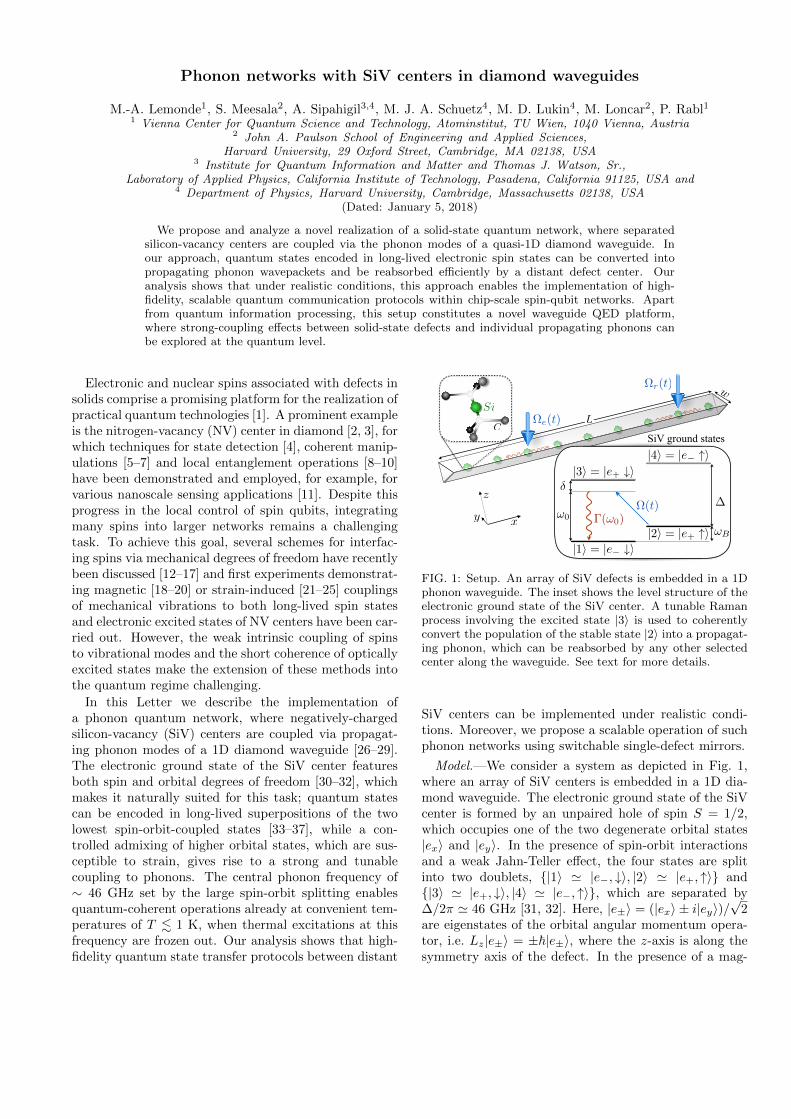
Phonon networks with SiV centers in diamond waveguides M.-A. Lemonde 1 , S. Meesala 2 , A. Sipahigil 3,4 , M. J. A. Schuetz 4 , M. D. Lukin 4 , M. Loncar 2 , P. Rabl 1 1 Vienna Center for Quantum Science and Technology, Atominstitut, TU Wien, 1040 Vienna, Austria 2 John A. Paulson School of Engineering and Applied Sciences, Harvard University, 29 Oxford Street, Cambridge, MA 02138, USA 3 Institute for Quantum Information and Matter and Thomas J. Watson, Sr., Laboratory of Applied Physics, California Institute of Technology, Pasadena, California 91125, USA and 4 Department of Physics, Harvard University, Cambridge, Massachusetts 02138, USA (Dated: January 5, 2018) We propose and analyze a novel realization of a solid-state quantum network, where separated silicon-vacancy centers are coupled via the phonon modes of a quasi-1D diamond waveguide. In our approach, quantum states encoded in long-lived electronic spin states can be converted into propagating phonon wavepackets and be reabsorbed efficiently by a distant defect center. Our analysis shows that under realistic conditions, this approach enables the implementation of high- fidelity, scalable quantum communication protocols within chip-scale spin-qubit networks. Apart from quantum information processing, this setup constitutes a novel waveguide QED platform, where strong-coupling effects between solid-state defects and individual propagating phonons can be explored at the quantum level. Electronic and nuclear spins associated with defects in solids comprise a promising platform for the realization of practical quantum technologies [1]. A prominent example is the nitrogen-vacancy (NV) center in diamond [2, 3], for which techniques for state detection [4], coherent manip- ulations [5–7] and local entanglement operations [8–10] have been demonstrated and employed, for example, for various nanoscale sensing applications [11]. Despite this progress in the local control of spin qubits, integrating many spins into larger networks remains a challenging task. To achieve this goal, several schemes for interfac- ing spins via mechanical degrees of freedom have recently been discussed [12–17] and first experiments demonstrat- ing magnetic [18–20] or strain-induced [21–25] couplings of mechanical vibrations to both long-lived spin states and electronic excited states of NV centers have been car- ried out. However, the weak intrinsic coupling of spins to vibrational modes and the short coherence of optically excited states make the extension of these methods into the quantum regime challenging. In this Letter we describe the implementation of a phonon quantum network, where negatively-charged silicon-vacancy (SiV) centers are coupled via propagat- ing phonon modes of a 1D diamond waveguide [26–29]. The electronic ground state of the SiV center features both spin and orbital degrees of freedom [30–32], which makes it naturally suited for this task; quantum states can be encoded in long-lived superpositions of the two lowest spin-orbit-coupled states [33–37], while a con- trolled admixing of higher orbital states, which are sus- ceptible to strain, gives rise to a strong and tunable coupling to phonons. The central phonon frequency of ∼ 46 GHz set by the large spin-orbit splitting enables quantum-coherent operations already at convenient tem- peratures of T . 1 K, when thermal excitations at this frequency are frozen out. Our analysis shows that high- fidelity quantum state transfer protocols between distant Si C ⌦ e (t) ⌦ r (t) δ Δ ! B ⌦(t) ! 0 |1i = |e - #i |3i = |e + #i |2i = |e + "i |4i = |e - "i SiV ground states w L Γ(! 0 ) x y z FIG. 1: Setup. An array of SiV defects is embedded in a 1D phonon waveguide. The inset shows the level structure of the electronic ground state of the SiV center. A tunable Raman process involving the excited state |3i is used to coherently convert the population of the stable state |2i into a propagat- ing phonon, which can be reabsorbed by any other selected center along the waveguide. See text for more details. SiV centers can be implemented under realistic condi- tions. Moreover, we propose a scalable operation of such phonon networks using switchable single-defect mirrors. Model.—We consider a system as depicted in Fig. 1, where an array of SiV centers is embedded in a 1D dia- mond waveguide. The electronic ground state of the SiV center is formed by an unpaired hole of spin S =1/2, which occupies one of the two degenerate orbital states |e x i and |e y i. In the presence of spin-orbit interactions and a weak Jahn-Teller effect, the four states are split into two doublets, {|1i ’ |e - , ↓i, |2i ’ |e + , ↑i} and {|3i’|e + , ↓i, |4i’|e - , ↑i}, which are separated by Δ/2π ’ 46 GHz [31, 32]. Here, |e ± i =(|e x i± i|e y i)/ √ 2 are eigenstates of the orbital angular momentum opera- tor, i.e. L z |e ± i = ±~|e ± i, where the z-axis is along the symmetry axis of the defect. In the presence of a mag-
Transcript of Phonon networks with SiV centers in diamond waveguides · Phonon networks with SiV centers in...
Phonon networks with SiV centers in diamond waveguides
M.-A. Lemonde1, S. Meesala2, A. Sipahigil3,4, M. J. A. Schuetz4, M. D. Lukin4, M. Loncar2, P. Rabl11 Vienna Center for Quantum Science and Technology, Atominstitut, TU Wien, 1040 Vienna, Austria
2 John A. Paulson School of Engineering and Applied Sciences,Harvard University, 29 Oxford Street, Cambridge, MA 02138, USA
3 Institute for Quantum Information and Matter and Thomas J. Watson, Sr.,Laboratory of Applied Physics, California Institute of Technology, Pasadena, California 91125, USA and
4 Department of Physics, Harvard University, Cambridge, Massachusetts 02138, USA(Dated: January 5, 2018)
We propose and analyze a novel realization of a solid-state quantum network, where separatedsilicon-vacancy centers are coupled via the phonon modes of a quasi-1D diamond waveguide. Inour approach, quantum states encoded in long-lived electronic spin states can be converted intopropagating phonon wavepackets and be reabsorbed efficiently by a distant defect center. Ouranalysis shows that under realistic conditions, this approach enables the implementation of high-fidelity, scalable quantum communication protocols within chip-scale spin-qubit networks. Apartfrom quantum information processing, this setup constitutes a novel waveguide QED platform,where strong-coupling effects between solid-state defects and individual propagating phonons canbe explored at the quantum level.
Electronic and nuclear spins associated with defects insolids comprise a promising platform for the realization ofpractical quantum technologies [1]. A prominent exampleis the nitrogen-vacancy (NV) center in diamond [2, 3], forwhich techniques for state detection [4], coherent manip-ulations [5–7] and local entanglement operations [8–10]have been demonstrated and employed, for example, forvarious nanoscale sensing applications [11]. Despite thisprogress in the local control of spin qubits, integratingmany spins into larger networks remains a challengingtask. To achieve this goal, several schemes for interfac-ing spins via mechanical degrees of freedom have recentlybeen discussed [12–17] and first experiments demonstrat-ing magnetic [18–20] or strain-induced [21–25] couplingsof mechanical vibrations to both long-lived spin statesand electronic excited states of NV centers have been car-ried out. However, the weak intrinsic coupling of spinsto vibrational modes and the short coherence of opticallyexcited states make the extension of these methods intothe quantum regime challenging.
In this Letter we describe the implementation ofa phonon quantum network, where negatively-chargedsilicon-vacancy (SiV) centers are coupled via propagat-ing phonon modes of a 1D diamond waveguide [26–29].The electronic ground state of the SiV center featuresboth spin and orbital degrees of freedom [30–32], whichmakes it naturally suited for this task; quantum statescan be encoded in long-lived superpositions of the twolowest spin-orbit-coupled states [33–37], while a con-trolled admixing of higher orbital states, which are sus-ceptible to strain, gives rise to a strong and tunablecoupling to phonons. The central phonon frequency of∼ 46 GHz set by the large spin-orbit splitting enablesquantum-coherent operations already at convenient tem-peratures of T . 1 K, when thermal excitations at thisfrequency are frozen out. Our analysis shows that high-fidelity quantum state transfer protocols between distant
Si
Ce(t)
r(t)
!B
(t)!0
|1i = |e #i
|3i = |e+ #i
|2i = |e+ "i
|4i = |e "iSiV ground states
w
L
(!0)xy
z
FIG. 1: Setup. An array of SiV defects is embedded in a 1Dphonon waveguide. The inset shows the level structure of theelectronic ground state of the SiV center. A tunable Ramanprocess involving the excited state |3〉 is used to coherentlyconvert the population of the stable state |2〉 into a propagat-ing phonon, which can be reabsorbed by any other selectedcenter along the waveguide. See text for more details.
SiV centers can be implemented under realistic condi-tions. Moreover, we propose a scalable operation of suchphonon networks using switchable single-defect mirrors.
Model.—We consider a system as depicted in Fig. 1,where an array of SiV centers is embedded in a 1D dia-mond waveguide. The electronic ground state of the SiVcenter is formed by an unpaired hole of spin S = 1/2,which occupies one of the two degenerate orbital states|ex〉 and |ey〉. In the presence of spin-orbit interactionsand a weak Jahn-Teller effect, the four states are splitinto two doublets, |1〉 ' |e−, ↓〉, |2〉 ' |e+, ↑〉 and|3〉 ' |e+, ↓〉, |4〉 ' |e−, ↑〉, which are separated by∆/2π ' 46 GHz [31, 32]. Here, |e±〉 = (|ex〉 ± i|ey〉)/
√2
are eigenstates of the orbital angular momentum opera-tor, i.e. Lz|e±〉 = ±~|e±〉, where the z-axis is along thesymmetry axis of the defect. In the presence of a mag-
2
netic field ~B = B0~ez, the Hamilton operator for a singleSiV center is (~ = 1)
HSiV = ωB |2〉〈2|+ ∆|3〉〈3|+ (∆ + ωB)|4〉〈4|
+1
2
[Ω(t)ei[ωdt+θ(t)] (|2〉〈3|+ |1〉〈4|) + H.c.
],
(1)
where ωB = γsB0 and γs is the spin gyromagnetic ratio.In Eq. (1), we have included a time-dependent drivingfield with a tunable Rabi-frequency Ω(t) and phase θ(t),which couples the lower and upper states of opposite spin.This coupling can be implemented either directly with amicrowave field of frequency ωd ∼ ∆ [38], or indirectlyvia an equivalent optical Raman process [39]. The lat-ter method is already used in experiments to initializeand prepare individual SiV centers in superpositions of|1〉 and |2〉 [33–35] with coherence times that can exceed10 ms in the absence of thermal processes and with dy-namical decoupling [36]. Further details on the derivationof HSiV are given in the supplementary material [39].
For the waveguide, we consider a quasi-1D geometryof width w and length L w. The waveguide supportstravelling phonon modes of frequency ωn,k and modefunction ~un,k(~r) ∼ ~u⊥n,k(y, z)eikx, where k is the wavevec-tor along the waveguide direction, n is the branch indexand ~u⊥n,k(y, z) is the transverse profile of the displace-ment field. The phonons induce transitions between theorbital states |e±〉 [40–42], and the Hamiltonian for thewhole system reads
H =∑j
H(j)SiV +
∑n,k
ωn,ka†n,kan,k
+1√L
∑j,k,n
(gjn,kJ
j+an,ke
ikxj + H.c.).
(2)
Here j labels the SiV centers located at positions ~rj =(xj , yj , zj), J− = (J+)† = |1〉〈3| + |2〉〈4| is the spin-
conserving lowering operator and an,k (a†n,k) are the anni-hilation (creation) operators for the phonon modes. Thecouplings gjn,k ≡ gn,k(yj , zj) depend on the components
of the local strain tensor, εabn,k(~rj) = 12 [ ∂∂xb
uan,k(~rj) +∂∂xa
ubn,k(~rj)], and can be evaluated for a known trans-
verse mode profile ~u⊥n (y, z) [39, 42]. We express the re-sulting couplings as
gjn,k = d
√~k2
2ρAωn,kξn,k(yj , zj), (3)
where d/2π ∼ 1 PHz is the strain sensitivity of the or-bital states [40, 41], ρ the density and A the transversearea of the waveguide. The dimensionless coupling pro-file ξn,k(y, z) accounts for the specific strain distributionand ξ(y, z) = 1 for a homogeneous compression mode.
From cavity to waveguide QED.—For small structures,L ∼ 10 − 100µm, w . 200 nm, and group velocities
10
30
50
70
0
0.7
0.8
0.9
1.0
1.1
1.2
0.1
0.2
0.3
0.4
0.5
0.6
20 40 60 800
1
2
3
4 z
z (nm)
k (µm1)10 20 30 40 50
l'
!/2
[GH
z]
s.l.s.t.
s.l.
s.t.
/2
[MH
z]
l
t
l/
2
[MH
z]
(a) (b)
(c) (d)
a.l.a.t.
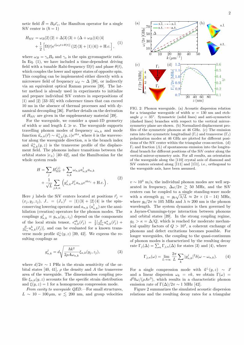
FIG. 2: Phonon waveguide. (a) Acoustic dispersion relationfor a triangular waveguide of width w = 130 nm and etch-angle ϕ = 35o. Symmetric (solid lines) and anti-symmetric(dashed lines) branches with respect to the vertical mirror-symmetry plane are shown. (b) Normalized displacement pro-files of the symmetric phonons at 46 GHz. (c) The emissionrates into the symmetric longitudinal (Γl) and transverse (Γt)polarization modes at 46 GHz are plotted for different posi-tions of the SiV center within the triangular cross-section. (d)Γl and fraction (βl) of spontaneous emission into the longitu-dinal branch for different positions of the SiV center along thevertical mirror-symmetry axis. For all results, an orientationof the waveguide along the [110] crystal axis of diamond andSiV centers oriented along [111] and [111], i.e., orthogonal tothe waveguide axis, have been assumed.
v ∼ 104 m/s, the individual phonon modes are well sep-arated in frequency, ∆ω/2π & 50 MHz, and the SiVcenters can be coupled to a single standing-wave modewith a strength gL = g0
√λ/L ≈ 2π × (4 − 14) MHz,
where g0/2π ≈ 105 MHz and λ ≈ 200 nm is the phononwavelength. The system dynamics is then governed bya Jaynes-Cummings-type interaction between phononsand orbital states [39]. In the strong coupling regime,gL > κ = ∆/Q, which is reached for moderate mechan-ical quality factors of Q > 104, a coherent exchange ofphonons and defect excitations becomes possible. Forlonger waveguides, the coupling to the quasi-continuumof phonon modes is characterized by the resulting decayrate Γj(∆) =
∑n Γj,n(∆) for states |3〉 and |4〉, where
Γj,n(ω) = limL→∞
2π
L
∑k
|gjn,k|2δ(ω − ωn,k). (4)
For a single compression mode with ~u⊥(y, z) ∼ ~xand a linear dispersion ωk = vk, we obtain Γ(ω) =d2~ω/(ρAv3), which results in a characteristic phononemission rate of Γ(∆)/2π ∼ 1 MHz [42].
Figure 2 summarizes the simulated acoustic dispersionrelations and the resulting decay rates for a triangular

3
waveguide [26, 40] of width w = 130 nm. The SiV cen-ters couple primarily to a longitudinal (l) compressionand a transverse (t) flexural mode with group velocitiesvl = 1.71 × 10⁴ m/s and vt = 0.73 × 10⁴ m/s, respec-tively. The coupling to the other two branches of oddsymmetry can be neglected for defects near the centerof the waveguide. Fig. 2(c) and (d) show that the ratesΓl,t are quite insensitive to the exact location of the SiVcenter. However, the fraction of phonons emitted into aspecific branch, βn = Γn/Γ, is significantly below unityas emission is split between a pair of modes. In opticalwaveguides [43], a value of β < 1 usually arises from theemission of photons into non-guided modes, which areirreversibly lost. For a phonon waveguide this is not thecase, but the multi-branch nature of the waveguide mustbe fully taken into account. In all examples below weassume βl = βt = 0.5, which is most relevant for SiVdefects located near the center of the beam.
Coherent spin-phonon interface.—We are interested inthe transfer of a qubit state, encoded into the stablestates |1〉 and |2〉, between an arbitrary pair of emitting(e) and receiving (r) defects in the waveguide,
(α|1〉e + β|2〉e)|1〉r → |1〉e(α|1〉r + β|2〉r). (5)
As shown in Fig. 1, this can be achieved by inducinga Raman transition via state |3〉e to convert the popu-lation in state |2〉e into a propagating phonon and byreverting the process at the receiving center. For lowenough temperatures, T ~∆/kB ≈ 2.2 K, such thatall phonon modes are initially in the vacuum state, thisscenario is described by the following ansatz for the wave-function |ψ(t)〉 = [α1 + βC†(t)]|1, 0〉, where |1, 0〉 isthe ground state with all SiV centers in state |1〉 andC†(t) =
∑j=e,r
[cj(t)e
−iωBt|2〉j〈1|+ bj(t)e−iω0t|3〉j〈1|+∑
n,k cn,k(t)e−iω0ta†n,k]
creates a single excitation dis-tributed between the SiV centers and the phonon modes.The central phonon frequency ω0 = ∆j + δj is assumedto be fixed by compensating small inhomogeneities in the∆j by the detunings δj = ωjd − (∆j − ωjB).
By adiabatically eliminating the fast decaying ampli-tudes bj , we derive effective equations of motion for theslowly varying amplitudes ci(t). From this derivation,detailed in [39], we obtain for each qubit amplitude
cj(t) = −γj(t)2
cj(t)−∑n
√γj,n(t)
2e−iθj(t)Φin
j,n(t), (6)
where γj(t) =∑n γj,n(t) is the effective decay rate of
state |2〉j and
γj,n(t) =Ω2j (t)
4δ2j + Γ2
j (ω0)Γj,n(ω0). (7)
Assuming 0 ≤ Ω(t)/2π < 70 MHz and δ/2π = 100 MHz,this rate can be tuned between γj = 0 and a maximal
value of γmax/2π ≈ 250 kHz, which is still fast comparedto the expected bare dephasing times T ∗2 = 10−100µs ofthe qubit state [36]. At the same time, the large detuningδ Γ(∆) ensures that any residual scattering of phononsfrom an undriven defect is strongly suppressed [39].
The last term in Eq. (6), where Φinj,n = Φin,L
j,n + Φin,Rj,n ,
describes the coupling of an SiV center to the left- (L)
and right- (R) incoming fields Φin,R/Lj,n , which themselves
are related to the corresponding outgoing fields by [44]
Φout,R/Lj,n (t) = Φ
in,R/Lj,n (t) +
√γj,n(t)
2cj(t)e
iθj(t). (8)
Together with Eq. (6), these input-output relations spec-ify the local dynamics at each node and must be sup-plemented by a set of propagation relations for all fields[cf. Fig. 3(a)]. As an example, for xr > xe, the rightpropagating fields obey Φin,R
r,n (t) = Φout,Re,n (t − τner)eiφ
ner ,
where τner = (xr − xe)/vn and φner = kn(xr − xe) arethe respective propagation times and phases. Reflec-tions at the boundaries lead to a retarded interactionof each center with its own emitted field. For example,Φin,Re,n (t) = −√RnΦout,L
e,n (t− τne )eiφne , where τne = 2xe/vn
and φne = 2knxe, and the reflectivity Rn ≤ 1 has beenintroduced to model losses. The combined set of time-nonlocal equations for the SiV amplitudes can be solvednumerically for given positions xj and pulses γj,n(t).Since any deterministic phase acquired during the proto-col can be undone by a local qubit rotation, we identifyF(t) = |cr(t)|2 with the fidelity of the transfer, whichexceeds the classical bound for F > 2/3 [45].Quantum state transfer.—In Fig. 3(b) we first consider
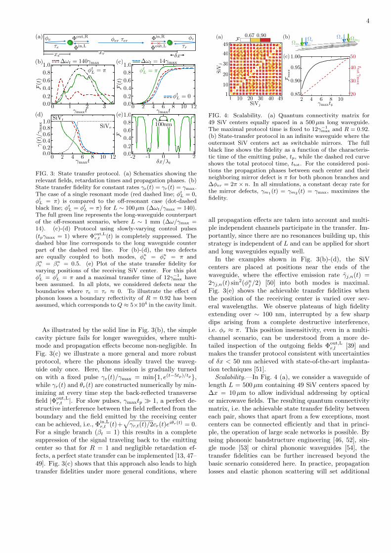
constant rates γj,n(t) = γmax/2, in which case a statetransfer is achieved over multiple round-trips of the emit-ted wave-packet. For L ∼ 100µm, the round-trip times2L/vn are still short compared to γ−1
max and we recoverthe standing-wave picture with splittings ∆ωn = πvn/Lbetween consecutive k-modes. When only the transversemode is resonant, [i.e., φtL = φte+φtr + 2φter = 2πn, whileφlL = (2m + 1)π] and for maximal coupling [φle = φlr =(2m + 1)π], we observe damped oscillations with a fastfrequency g =
√γmax∆ωt/2π ≈ 2π × 1.2 MHz and de-
cay rate κ = −∆ωπ logR ≈ 2π × 0.93 MHz. This result
is expected from a single-mode description of the waveg-uide [39], and is recovered here as a limiting case of ourgeneral framework. The losses from multiple imperfectreflections at the boundaries can be partially suppressedat the expense of a slightly slower transfer by detuningthe SiV centers from the closest mode by δ0 > g. Inthis case the SiV centers communicate via an exchangeof virtual phonons and κ → κ(g/δ0)2. For a maximaldetuning δ0 = ∆ωt/2, the transfer fidelity scales approx-imately as F ' R − π2/(8T ∗2 γmax) [39]. For T ∗2 ≈ 100µsand R > 0.99, which can be achieved, for example, byphononic Bragg mirrors [46], gate fidelities of F & 0.99are possible.
4
maxt maxt
r
e
e
r
erer
xexr x
in,R
in,L out,L
out,R(t
)/m
ax
0 4 8
F(t
)
12
0.0
0.2
0.4
0.6
0.8
1.0
x/t
-2 -1 0 1 2
30 1 2 2 6 10
100nm
!t = 14max!t = 140max
F(t
)
0.0
0.2
0.4
0.6
0.8
1.0
0.0
0.2
0.4
0.6
0.8
1.0
maxt0 4 8 122 6 10
SiVe
SiVr
0.00.20.40.60.81.0
F
(a)
(b) (c)
(d) (e)
tL =
tL = 0
tL =
FIG. 3: State transfer protocol. (a) Schematics showing therelevant fields, retardation times and propagation phases. (b)State transfer fidelity for constant rates γe(t) = γr(t) = γmax.The case of a single resonant mode (red dashed line; φt
L = 0,φlL = π) is compared to the off-resonant case (dot-dashed
black line; φtL = φl
L = π) for L ∼ 100µm (∆ωt/γmax = 140).The full green line represents the long-waveguide counterpartof the off-resonant scenario, where L ∼ 1 mm (∆ω/γmax =14). (c)-(d) Protocol using slowly-varying control pulses
(tpγmax = 1) where Φout,Lr,t (t) is completely suppressed. The
dashed blue line corresponds to the long waveguide counterpart of the dashed red line. For (b)-(d), the two defectsare equally coupled to both modes, φn
e = φnr = π and
βne = βn
r = 0.5. (e) Plot of the state transfer fidelity forvarying positions of the receiving SiV center. For this plotφtL = φl
L = π and a maximal transfer time of 12γ−1max have
been assumed. In all plots, we considered defects near theboundaries where τe = τr ≈ 0. To illustrate the effect ofphonon losses a boundary reflectivity of R = 0.92 has beenassumed, which corresponds to Q ≈ 5×10⁴ in the cavity limit.
As illustrated by the solid line in Fig. 3(b), the simplecavity picture fails for longer waveguides, where multi-mode and propagation effects become non-negligible. InFig. 3(c) we illustrate a more general and more robustprotocol, where the phonons ideally travel the waveg-uide only once. Here, the emission is gradually turnedon with a fixed pulse γe(t)/γmax = min1, e(t−5tp)/tp,while γr(t) and θr(t) are constructed numerically by min-imizing at every time step the back-reflected transversefield |Φout,L
r,t |. For slow pulses, γmaxtp 1, a perfect de-structive interference between the field reflected from theboundary and the field emitted by the receiving centercan be achieved, i.e., Φin,L
r,t (t)+√γr,t(t)/2cr(t)e
iθr(t) = 0.For a single branch (βt = 1) this results in a completesuppression of the signal traveling back to the emittingcenter so that for R = 1 and negligible retardation ef-fects, a perfect state transfer can be implemented [13, 47–49]. Fig. 3(c) shows that this approach also leads to hightransfer fidelities under more general conditions, where
2 4 6
F max
tto
t m
ax
108
1.00
0.95
0.90
0.85 20
40
50
30
er
m1
m2
1 10 20 30 40 491
10
20
30
40
49
SiVj
SiV
j
0.67 0.90F(a) (b)
(c)
maxtp
FIG. 4: Scalability. (a) Quantum connectivity matrix for49 SiV centers equally spaced in a 500µm long waveguide.The maximal protocol time is fixed to 12γ−1
max and R = 0.92.(b) State-transfer protocol in an infinite waveguide where theoutermost SiV centers act as switchable mirrors. The fullblack line shows the fidelity as a function of the characteris-tic time of the emitting pulse, tp, while the dashed red curveshows the total protocol time, ttot. For the considered posi-tions the propagation phases between each center and theirneighboring mirror defect is π for both phonon branches and∆φer = 2π × n. In all simulations, a constant decay rate forthe mirror defects, γm1(t) = γm2(t) = γmax, maximizes thefidelity.
all propagation effects are taken into account and multi-ple independent channels participate in the transfer. Im-portantly, since there are no resonances building up, thisstrategy is independent of L and can be applied for shortand long waveguides equally well.
In the examples shown in Fig. 3(b)-(d), the SiVcenters are placed at positions near the ends of thewaveguide, where the effective emission rate γj,n(t) =2γj,n(t) sin2(φnj /2) [50] into both modes is maximal.Fig. 3(e) shows the achievable transfer fidelities whenthe position of the receiving center is varied over sev-eral wavelengths. We observe plateaus of high fidelityextending over ∼ 100 nm, interrupted by a few sharpdips arising from a complete destructive interference,i.e. φr ≈ π. This position insensitivity, even in a multi-channel scenario, can be understood from a more de-tailed inspection of the outgoing fields Φout,L
r,l [39] andmakes the transfer protocol consistent with uncertaintiesof δx < 50 nm achieved with state-of-the-art implanta-tion techniques [51].
Scalability.—In Fig. 4 (a), we consider a waveguide oflength L = 500µm containing 49 SiV centers spaced by∆x = 10µm to allow individual addressing by opticalor microwave fields. The resulting quantum connectivitymatrix, i.e. the achievable state transfer fidelity betweeneach pair, shows that apart from a few exceptions, mostcenters can be connected efficiently and that in princi-ple, the operation of large scale networks is possible. Byusing phononic bandstructure engineering [46, 52], sin-gle mode [53] or chiral phononic waveguides [54], thetransfer fidelities can be further increased beyond thebasic scenario considered here. In practice, propagationlosses and elastic phonon scattering will set additional

5
limitations for the overall size of the network. In Fig. 4(b), we show a general strategy to overcome these lim-itations by separating the whole waveguide into smallersegments using additional ‘mirror centers’. Here thetwo outermost SiV centers simply reflect the incomingphonon wavepacket [55], and thus create an effective cav-ity within the waveguide [56, 57]. This is illustrated inFig. 4 (b), where we plot the resulting state transfer fi-delity for two SiV centers localized inside this effectivecavity. For transfer pulses that are long compared toγ−1
max, the outmost centers act as almost perfect mirrors,such that even in an infinite waveguide state transfer pro-tocols within reconfigurable sections of the network canbe implemented.
Conclusion.—We have shown how an efficient couplingbetween individual SiV centers and propagating phononsin a diamond waveguide can be realized and used forquantum networking applications. By employing directspin-phonon couplings in the presence of a transversemagnetic field [58] or defect-phonon interactions in othermaterials [59–61], many of the described techniques couldalso be adapted for lower phonon frequencies ∼ 5 − 10GHz, where many advanced phononic engineering meth-ods are already available. When combined with localcontrol operations involving adjacent nuclear spins asquantum memories [10, 33, 62, 63], the set of all thesetechniques provides a realistic approach for a scalablequantum information processing platform with spins insolids.
Acknowledgements.—This work was supported by theAustrian Science Fund (FWF) through the SFB FoQuS,Grant No. F40, the START Grant No. Y 591-N16,ONR MURI on Quantum Optomechanics (Award No.N00014-15-1-2761), STC Center for Integrated QuantumMaterials (NSF Grant No. DMR-1231319), NSF EFRIACQUIRE (Award No. 5710004174), CUA, NSF andVannevar Bush Fellowship.
[1] T. D. Ladd, F. Jelezko, R. Laflamme, Y. Nakamura, C.Monroe, and J. L. O’Brien, Quantum computers, Nature(London) 464, 7285 (2010).
[2] M. W. Doherty, N. B. Manson, P. Delaney, F. Jelezko,J. Wrachtrup, and L. C. L. Hollenberg, The nitrogen-vacancy colour centre in diamond, Phys. Rep. 528, 1(2013).
[3] L. Childress, R. Walsworth, and M. D. Lukin, Atom-likecrystal defects, Phys. Today 67, 38 (2014).
[4] F. Jelezko, T. Gaebel, I. Popa, A. Gruber, and J.Wrachtrup, Observation of coherent oscillations in a sin-gle electron spin, Phys. Rev. Lett. 92, 076401 (2004).
[5] L. Childress, M.V. Gurudev Dutt, J. M. Taylor, A. S.Zibrov, F. Jelezko, J. Wrachtrup, P. R. Hemmer, andM. D. Lukin, Coherent Dynamics of Coupled Electronand Nuclear Spin Qubits in Diamond, Science 314, 5797(2006).
[6] G. de Lange, Z. H. Wang, D. Riste, V. V. Dobrovitski,and R. Hanson, Universal Dynamical Decoupling of aSingle Solid-State Spin from a Spin Bath, Science 330,60 (2010).
[7] L. C. Bassett, F. J. Heremans, D. J. Christle, C. G. Yale,G. Burkard, B. B. Buckley, and D. D. Awschalom, Ul-trafast optical control of orbital and spin dynamics in asolid-state defect, Science 345, 6202 (2014).
[8] W. Pfaff, T. H. Taminiau, L. Robledo, H. Bernien, M.Markham, D. J. Twitchen, and R. Hanson, Demon-stration of entanglement-by-measurement of solid-statequbits, Nat. Phys. 9, 29 (2013).
[9] F. Dolde, I. Jakobi, B. Naydenov, N. Zhao, S. Pezzagna,C. Trautmann, J. Meijer, P. Neumann, F. Jelezko, andJ. Wrachtrup, Room-temperature entanglement betweensingle defect spins in diamond, Nat. Phys. 9, 139 (2013).
[10] G. Waldherr, Y. Wang, S. Zaiser, M. Jamali, T. Schulte-Herbruggen, H. Abe, T. Ohshima, J. Isoya, J. F. Du,P. Neumann, and J. Wrachtrup, Quantum error correc-tion in a solid-state hybrid spin register, Nature (London)506, 204 (2014).
[11] L. Rondin, J.-P. Tetienne, T. Hingant, J.-F. Roch,P. Maletinsky, and V. Jacques, Magnetometry withnitrogen-vacancy defects in diamond, Rep. Prog. Phys.77, 056503 (2014).
[12] P. Rabl, S. J. Kolkowitz, F. H. Koppens, J. G. E. Harris,P. Zoller, and M. D. Lukin, A quantum spin transducerbased on nanoelectromechanical resonator arrays, Nat.Phys. 6, 602 (2010).
[13] S. J. M. Habraken, K. Stannigel, M. D. Lukin, P. Zoller,and P. Rabl, Continuous mode cooling and phononrouters for phononic quantum networks, New J. Phys.14, 115004 (2012).
[14] S. D. Bennett, N. Y. Yao, J. Otterbach, P. Zoller, P.Rabl, and M. D. Lukin, Phonon-Induced Spin-Spin In-teractions in Diamond Nanostructures: Application toSpin Squeezing, Phys. Rev. Lett., 110, 156402 (2013).
[15] A. Albrecht, A. Retzker, F. Jelezko, and M. B. Plenio,Coupling of nitrogen vacancy centres in nanodiamondsby means of phonons, New J. Phys. 15, 083014 (2013).
[16] M. J. A. Schuetz, E. M. Kessler, G. Giedke, L. M. K.Vandersypen, M. D. Lukin, and J. I. Cirac, UniversalQuantum Transducers Based on Surface Acoustic Waves,Phys. Rev. X 5, 031031 (2015).
[17] D. Lee, K. W. Lee, J. V. Cady, P. Ovartchaiyapong andA. C. Bleszynski Jayich, Topical review: spins and me-chanics in diamond, J. Opt. 19, 033001 (2017).
[18] D. Rugar, R. Budakian, H. J. Mamin, and B. W. Chui,Single spin detection by magnetic resonance force mi-croscopy, Nature (London) 430, 329 (2004).
[19] O. Arcizet, V. Jacques, A. Siria, P. Poncharal, P. Vincent,and S. Seidelin, A single nitrogen-vacancy defect coupledto a nanomechanical oscillator, Nat. Phys. 7, 879 (2011).
[20] S. Kolkowitz, A. C. Bleszynski Jayich, Q. P. Unterreith-meier, S. D. Bennett, P. Rabl, J. G. Harris, and M. D.Lukin, Coherent Sensing of a Mechanical Resonator witha Single-Spin Qubit, Science 335, 1603 (2012).
[21] E. R. MacQuarrie, T. A. Gosavi, N. R. Jungwirth, S.A. Bhave, and G. D. Fuchs, Mechanical Spin Control ofNitrogen-Vacancy Centers in Diamond, Phys. Rev. Lett.111, 227602 (2013).
[22] P. Ovartchaiyapong, K. W. Lee, B. A. Myers, and A. C.Bleszynski Jayich, Dynamic strain-mediated coupling ofa single diamond spin to a mechanical resonator, Nat.

6
Commun. 5, 4429 (2014).[23] A. Barfuss, J. Teissier, E. Neu, A. Nunnenkamp, and P.
Maletinsky, Strong mechanical driving of a single electronspin, Nat. Phys. 11, 820 (2015).
[24] D. A. Golter, T. Oo, M. Amezcua, K. A. Stewart,and H. Wang, Optomechanical Quantum Control of aNitrogen-Vacancy Center in Diamond, Phys. Rev. Lett.116, 143602 (2016).
[25] S. Meesala, Y.-I. Sohn, H. A. Atikian, S. Kim, M. J. Bu-rek, J. T. Choy, and M. Loncar, Enhanced Strain Cou-pling of Nitrogen-Vacancy Spins to Nanoscale DiamondCantilevers, Phys. Rev. Appl. 5, 034010 (2016).
[26] M. J. Burek, N. P. de Leon, B. J. Shields, B. J. M.Hausmann, Y. Chu, Q. Quan, A. S. Zibrov, H. Park,M. D. Lukin, and M. Loncar, Free-Standing Mechanicaland Photonic Nanostructures in Single-Crystal Diamond,Nano Lett. 12, 6084 (2012).
[27] B. Khanaliloo, H. Jayakumar, A. C. Hryciw, D. P. Lake,H. Kaviani, and P. E. Barclay, Single-Crystal DiamondNanobeam Waveguide Optomechanics, Phys. Rev. X 5,041051 (2015).
[28] A. Sipahigil, R. E. Evans, D. D. Sukachev, M. J. Bu-rek, J. Borregaard, M. K. Bhaskar, C. T. Nguyen, J.L. Pacheco, H. A. Atikian, C. Meuwly, R. M. Camacho,F. Jelezko, E. Bielejec, H. Park, M. Loncar, and M. D.Lukin, An integrated diamond nanophotonics platformfor quantum-optical networks, Science 354, 847 (2016).
[29] S. Mouradian, N. H. Wan, T. Schroder, and D. Englund,Rectangular photonic crystal nanobeam cavities in bulkdiamond, Appl. Phys. Lett. 111, 021103 (2017).
[30] J. P. Goss, R. Jones, S. J. Breuer, P. R. Briddon, and
S. Oberg, The Twelve-Line 1.682 eV Luminescence Cen-ter in Diamond and the Vacancy-Silicon Complex, Phys.Rev. Lett. 77, 3041 (1996).
[31] C. Hepp, T. Muller, V. Waselowski, J. N. Becker, B. Pin-gault, H. Sternschulte, D. Steinmuller-Nethl, A. Gali, J.R. Maze, M. Atature, and C. Becher, Electronic Struc-ture of the Silicon Vacancy Color Center in Diamond,Phys. Rev. Lett. 112, 036405 (2014).
[32] C. Hepp, Electronic Structure of the Silicon VacancyColor Center in Diamond, Ph.D. thesis, University ofSaarland (2014).
[33] L. J. Rogers, K. D. Jahnke, M. H. Metsch, A. Sipahigil, J.M. Binder, T. Teraji, H. Sumiya, J. Isoya, M. D. Lukin,P. Hemmer, and F. Jelezko, All-Optical Initialization,Readout, and Coherent Preparation of Single Silicon-Vacancy Spins in Diamond, Phys. Rev. Lett. 113, 263602(2014).
[34] J. N. Becker, J. Gorlitz, C. Arend, M. Markham, andC. Becher, Ultrafast all-optical coherent control of singlesilicon vacancy colour centres in diamond, Nat. Commun.7, 13512 (2016).
[35] Y. Zhou, A. Rasmita, K. Li, Q. Xiong, I. Aharonovich,and W.-B. Gao, Coherent control of a strongly drivensilicon vacancy optical transition in diamond, Nat. Com-mun. 8, 14451 (2017).
[36] D. D. Sukachev, A. Sipahigil, C. T. Nguyen, M. K.Bhaskar, R. E. Evans, F. Jelezko, and M. D. Lukin, Thesilicon-vacancy spin qubit in diamond: quantum memoryexceeding ten milliseconds and single-shot state readout,Phys. Rev. Lett. 119, 223602 (2017).
[37] J. N. Becker and C. Becher, Coherence properties andquantum control of silicon vacancy color centers in dia-
mond, Phys. Status Solidi A 214, 1700586 (2017).[38] J. J. Pla, K. Y. Tan, J. P. Dehollain, W. H. Lim, J. J. L.
Morton, D. N. Jamieson, A. S. Dzurak, and A. Morello,A single-atom electron spin qubit in silicon, Nature 489,541 (2012).
[39] See Supplemental Material for additional details aboutthe model and the state transfer protocols.
[40] Y.-I. Sohn, S. Meesala, B. Pingault, H. A. Atikian, J.Holzgrafe, M. Gundogan, C. Stavrakas, M. J. Stanley, A.Sipahigil, J. Choi, M. Zhang, J. L. Pacheco, J. Abraham,E. Bielejec, M. D. Lukin, M. Atature, and M. Loncar,Engineering a diamond spin-qubit with a nano-electro-mechanical system, arXiv:1706.03881.
[41] K. D. Jahnke, A. Sipahigil, J. M. Binder, M. W. Doherty,M. Metsch, L. J. Rogers, N. B. Manson, M. D. Lukinand F. Jelezko, Electron-phonon processes of the silicon-vacancy centre in diamond, New J. Phys. 17, 043011(2015).
[42] K. V. Kepesidis, M.-A. Lemonde, A. Norambuena, J.R. Maze, and P. Rabl, Cooling phonons with phonons:Acoustic reservoir engineering with silicon-vacancy cen-ters in diamond, Phys. Rev. B 94, 214115 (2016).
[43] P. Lodahl, S. Mahmoodian, and S. Stobbe, Interfacingsingle photons and single quantum dots with photonicnanostructures, Rev. Mod. Phys. 87, 347 (2015).
[44] C. W. Gardiner and P. Zoller, Quantum noise (Springer,Berlin; New York, 2000).
[45] S. Massar and S. Popescu, Optimal extraction of infor-mation from finite quantum ensembles, Phys. Rev. Lett.74, 1259 (1995).
[46] M. Maldovan, Sound and heat revolutions in phononics,Nature (London) 503, 209 (2013).
[47] J. I. Cirac, P. Zoller, H. J. Kimble, and H. Mabuchi,Quantum State Transfer and Entanglement Distributionamong Distant Nodes in a Quantum Network, Phys. Rev.Lett. 78, 3221 (1997).
[48] K. Jahne, B. Yurke, and U. Gavish, High-fidelity transferof an arbitrary quantum state between harmonic oscilla-tors, Phys. Rev. A 75, 010301 (2007).
[49] A. N. Korotkov, Flying microwave qubits with nearlyperfect transfer effciency, Phys. Rev. B 84, 014510(2011).
[50] U. Dorner and P. Zoller, Laser-driven atoms in half-cavities, Phys. Rev. A 66, 023816 (2002).
[51] T. Schroder, M. E. Trusheim, M. Walsh, L. Li, J. Zheng,M. Schukraft, A. Sipahigil, R. E. Evans, D. D. Sukachev,C. T. Nguyen, J. L. Pacheco, R. M. Camacho, E. S. Biele-jec, M. D. Lukin, and D. Englund, Scalable focused ionbeam creation of nearly lifetime-limited single quantumemitters in diamond nanostructures, Nat. Commun. 8,15376 (2017).
[52] A. H. Safavi-Naeini and O. Painter, Proposal for an op-tomechanical traveling wave phononphoton translator,New J. Phys. 13, 013017 (2011).
[53] R. N. Patel, Z. Wang, W. Jiang, C. J. Sarabalis, J. T.Hill, and A. H. Safavi-Naeini, A single-mode phononicwire, arXiv:1711.00847.
[54] C. Brendel, V. Peano, O. Painter, and F. Mar-quardt, Snowflake Topological Insulator for SoundWaves, arXiv:1701.06330.
[55] J. T. Shen and S. Fan, Coherent single photon trans-port in a one-dimensional waveguide coupled with su-perconducting quantum bits, Phys. Rev. Lett. 95,213001(2005).

7
[56] L. Zhou, H. Dong, Yu-xi Liu, C. P. Sun, and F. Nori,Quantum supercavity with atomic mirrors, Phys. Rev. A78, 063827 (2008).
[57] D. E. Chang, L. Jiang, A. V. Gorshkov, and H. J. Kim-ble, Cavity QED with atomic mirrors, New J. Phys. 14,063003 (2012).
[58] S. Meesala, Y-I. Sohn, et al., Strain engineering of thesilicon vacancy center in diamond, in preparation (2017).
[59] O. O. Soykal, R. Ruskov, and C. Tahan, Sound-BasedAnalogue of Cavity Quantum Electrodynamics in Silicon,Phys. Rev. Lett. 107, 235502 (2011).
[60] R. Ruskov and C. Tahan, On-chip cavity quantum phon-odynamics with an acceptor qubit in silicon, Phys. Rev.B 88, 064308 (2013).
[61] T. Ramos, V. Sudhir, K. Stannigel, P. Zoller, and T.
J. Kippenberg, Nonlinear Quantum Optomechanics viaIndividual Intrinsic Two-Level Defects, Phys. Rev. Lett.110, 193602 (2013).
[62] M. V. G. Dutt, L. Childress, L. Jiang, E. Togan, J.Maze, F. Jelezko, A. S. Zibrov, P. R. Hemmer, and M. D.Lukin, Quantum Register Based on Individual Electronicand Nuclear Spin Qubits in Diamond, Science 316, 5829(2007).
[63] A. Reiserer, N. Kalb, M. S. Blok, K. J. M. van Bem-melen, D. J. Twitchen, M. Markham, T. H. Taminiau,and R. Hanson, Robust quantum-network memory usingdecoherence-protected subspaces of nuclear spins, Phys.Rev. X 6, 021040 (2016).