PHOENIXDISPLAYIN TERNATIONAL,INC SPECIFICATIONFORLCD …
24
C P D V IS COMP Phoen 6150 Chand USA www (630) (630) PH CUSTOME PARTNUM DESCRIPTI VERSION SSUEDAT P ANYADDR nixDisplay W.GilaSpr dler,AZ852 w.phoenixdis 3595700o 3595701f PHO INTE HOENIX SPECIF R MBER P ION 3 1 TE 2 RESS Internation ringsPlaceU 226 splay.com office fax OENIX ERNAT XDISPL FICATIO PDIS039QW 3.9"480(R 1.0 22Apr20 nal,Inc. Unit2 XDISP TIONA LAYINT ONFOR WQ01HS RGB)x128 PLAY AL,IN TERNA T RLCDM DotsWQV NC. TIONAL MODUL VGA L,INC E
Transcript of PHOENIXDISPLAYIN TERNATIONAL,INC SPECIFICATIONFORLCD …

�
���
�
C
P
D
V
IS������������COMPPhoen6150�ChandUSA�www(630)�(630)�
PH
CUSTOME
PART�NUM
DESCRIPTI
VERSION
SSUE�DAT
PANY�ADDRnix�Display�W.�Gila�Sprdler,�AZ�852
w.phoenixdis359�5700�o359�5701�f
PHOINTE
�HOENIX
SPECIF
R
MBER PION 3
1TE 2
RESS �Internationrings�Place�U226�
splay.com�office�fax� � � � �
OENIXERNAT
�
X�DISPL
FICATIO
PDIS039QW3.9"�480(R1.022�Apr�20
nal,�Inc.�Unit�2�
X�DISPTIONA
LAY�INT�
ON�FOR
WQ01HSRGB)x128�
PLAY�AL,�IN
TERNAT
R�LCD�M
Dots�WQV
NC.�
TIONAL
MODUL
VGA�
L,�INC�
E�
�

SHENZHEN CDTECH ELECTRONICS
Page2 of 24
Table of Contents
1. Record of Revision................................................................................................................ 3
2. General Specifications..........................................................................................................4
3. Input/OutputTerminals...........................................................................................................5
4. Absolute Maximum Rating....................................................................................................5
5.Electrical Characteristics............................................................................................6
6. Interface Timing........................................................................................................8
7. Optical Characteristics........................................................................................................11
8. Environmental / Reliability Tests....................................................................................... 15
9. Mechanical Drawing............................................................................................................16
10. Packing................................................................................................................................17
11. TFT-LCD Module Inspection Criteria..............................................................................18
12. Precautions for Use of LCD modules............................................................................ 23

1. Record of Revision
Rev Issued Date Description Editor
1.0 2017/1/20 First Release. Jack Guo
1.0 2020/4/22 change the Print P/N into Label ZHP

2. General SpecificationsFeature Spec
Characteristics
Size 3.9 inchResolution 480(horizontal)*128(Vertical)Interface RGB-24bit(HV mode)Connect type ConnectorDisplay Colors 16.7MTechnology type a-SiPixel pitch (mm) 0.198*0.198Pixel Configuration R.G.B.-StripeDisplay Mode Normally WhiteDriver IC ILI6480Viewing Direction 12 O’clock
Mechanical
LCM (W x H x D) (mm) 105.50*40.64*2.95Active Area(mm) 95.04*25.34With /Without TSP Without TSPWeight (g) TBDLED Numbers 10 LEDs
Note 1: Requirements on Environmental Protection: RoHsNote 2: LCM weight tolerance: +/- 5%

3. Input/OutputTerminals
No. Symbol Description
1 VBL- Backlight LED Cathode2 VBL+ Backlight LED Anode.3 GND System Ground4 VDD Power supply for logic operation
5~12 R0~R7 Data bus13~20 G0~G7 Data bus21~28 B0~B7 Data bus
29 GND System Ground30 CLK Pixel clock signal31 DISP Display on/off control32 HSYNC Horizontal Sync signal33 VSYNC Vertical Sync signal
34 DEN Data EnableRemark: internal pulled weak low
35 NC No connection36 GND System Ground37 XR(NC) The right side signal of TP38 YD(NC) The down side signal of TP39 XL(NC) The left side signal of TP40 YU(NC) The up side signal of TP
4. Absolute Maximum RatingItem Symbol MIN Typ MAX Unit Remark
Supply Voltage VDD -0.5 - 5.0 V -
Operating Temperature TOPR -20 - 70 -
Storage Temperature TSTG -30 - 80

5. Electrical Characteristics5.1 Driving TFT LCD Panel
Item Symbol MIN TYP MAX Unit Remark
Supply Voltage VDD 3.0 3.3 3.6 V
Input Signal
Voltage
Low Leve VIL GND - 0.3x VDD V
High Level VIH 0.7x VDD - VDD V
Output Signal
Voltage
Low Leve VOL GND - VDD+0.4 V
High Level VOH VDD-0.4 - - V
5.2 LED Driving ConditionsItem Symbol MIN TYP MAX Unit Remark
Forward Current IF - 40 50 mA
Forward Voltage VF 16 17 18 V
Backlight Power consumption WBL - 0.68 - W
LED Lifetime - 25000 - Hrs
Note 1: Each LED: IF =20 mA, VF =3.2+/0.2V.
Note 2: Optical performance should be evaluated at Ta=25 only.
Note 3: If LED is driven by high current, high ambient temperature & humidity condition. The life
Time of LED will be reduced. Operating life means brightness goes down to 50% initial brightness.
Typical operating life time is estimated data.
Figure: LED connection of backlight(Constant Current)

5.3 Block Diagram
Power
BLU
3.9 inch480(RGB )*128
LCD Panel
Source+Gate Driver
GrayscaleManipulationVoltage
VCOM
R(0:7),G(0:7),B(0:7),HSN,VSN,CLK, DEN
VDD,GND
VLED+,VLED-
FPC
RGB656
BLU

6. Interface Timing
6.1 Timing relationship among DE, Source Output, Gate Output, Vcom
6.2 Parallel RGB Data Format

Parameter Symbol Value Unit
Min Typ Max
DCLK frequency FCLK 5 9 12 MHZ
VSD period time TV 133 144 256 H
VSD display area TVD 128 128 128 H
VSD back porch TVB 3 8 31 H
VSD front porch TVFP 2 8 97 H
HSD period time TH 520 525 800 DCLK
HSD display area THD 480 480 480 DCLK
HSD back porch THBP 36 40 255 DCLK
HSD front porch THFP 4 5 65 DCLK
6.3 Output Timing Diagram


7. Optical CharacteristicsItems Symbol Condition Min. Typ. Max. Unit Remark Note
Response time Tr+Tf-
- 25 50 ms FIG.1 Note4
Contrast Ratio CR 400 500 - - FIG.2 Note1
Surfaceluminance LV =0° 450 500 - cd/m2 FIG.2 Note2
Luminanceuniformity Yu =0° 75 80 - % FIG.2 Note3
NTSC - =0° - 50 - % FIG.2 Note5
Viewing angle
�T
Center
CR�10
40 50 - deg FIG.3
Note6�B 60 70 - deg FIG.3�L 60 70 - deg FIG.3�R 60 70 - deg FIG.3
Chromaticity
RedRX
=0°
=0°
Ta=25°
TBD TBD TBD -
FIG.2CIE1931 Note5
RY TBD TBD TBD -
GreenGX TBD TBD TBD -GY TBD TBD TBD -
BlueBX TBD TBD TBD -BY TBD TBD TBD -
WhiteWX 0.26 0.31 0.36 -WY 0.28 0.33 0.38 -


8. Environmental / Reliability Tests
No Test Item Condition Remarks
1 High TemperatureOperation Ts= +70 , 96hrs
Note 1IEC60068-2-2,GB2423. 2-89
2 Low TemperatureOperation Ta= -20 , 96hrs Note 2 IEC60068-2-1
GB2423.1-89
3 High TemperatureStorage Ta= +80 , 96hrs IEC60068-2-2
GB2423. 2-89
4 Low TemperatureStorage Ta= -30 , 96hrs IEC60068-2-1
GB/T2423.1-89
5 High Temperature &Humidity Storage Ta= +60 , 90% RH max,96 hours IEC60068-2-3
GB/T2423.3-2006
6 Thermal Shock(Non-operation)
-20 30 min ~ +60 30 minChange time: 5min, 30 Cycle
Start with coldtemperature, end with
high temperatureIEC60068-2-14,GB2423.22-87
7Electro StaticDischarge(Operation)
C=150pF, R=330 �, 5 points/panelAir:±8KV, 5 times; Contact: ±4KV, 5
times; (Environment: 15 ~35 , 30% ~ 60%, 86Kpa ~ 106Kpa)
IEC61000-4-2GB/T17626.2-1998
8 Vibration(Non-operation)
Frequency range: 10~55Hz, Stroke:1.mm Sweep: 10Hz~55Hz~10Hz
2 hours for each direction of X .Y. Z.(package condition)
IEC60068-2-6GB/T2423.5-1995
9 Shock (Non-operation) 60G 6ms, ± X, ±Y , ± Z3 times for each direction
IEC60068-2-27GB/T2423.5-1995
10 Package Drop Test Height: 80 cm, 1 corner, 3 edges,6 surfaces
IEC60068-2-32GB/T2423.8-1995
Note: 1. TS is the temperature of panel’s surface.2. Ta is the ambient temperature of sample.3. The size of sample is 5pcs.
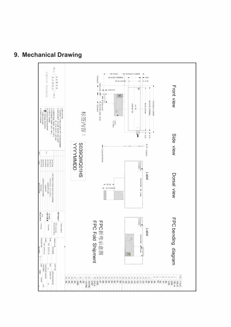
9. Mechanical Drawing
R1
GN
DNCNCNCNC V
BL-K
VBL-A
GN
DV
DD
NC
R3 R0R2G3
B0 R4R5R6B2B3B4B5B6B7GN
DD
CLK
B1 R7G0
G1
G4
G5
G6
G7
DISP
HS
YNC
VS
YNC
DE G2
RE
V.
PR
OJ
EC
TIO
N
DW
N
CH
KD
SP
EC
IFIEDm
mU
NIT
SC
ALE
TO
LER
AN
CE
UN
LES
S
SH
EE
T O
F
RE
V.
DA
TEM
OD
IFIC
ATIO
N
Gray
VIE
WIN
G
PA
RT NO
.
HZX
201
9.01.151.0
1/1±0.2
1:1
3rd
AN
GLE
RG
B Interfa
ce
FP
C C
onne
ctor(F
H1
2-40S
-0.5SH
)L
CM
-S03
9QW
Q01H
S10100095
LCM
NO
TES:
1. DIS
PLAY
TY
PE: 3.9 IN
CH
TFT /T
RA
NS
MISSIVE
2. BA
CK
LIGH
T: 10 CH
IP W
HITE
LED
, 5S2P
VF =
17±1.0V;IV
= 20*2m
A3. O
PER
ATIN
G T
EM
P: -20°C~+
70°C4. S
TOR
AG
E T
EM
P: -30°c~+80°c
5. LCD
IC: ILI6480
6.Luminance:500cd/m
2(TYP)7.
)"reference dimension.
"*"critical dimension
8. RoH
S C
ompliant
22.45
5.00±0.5
480
(RG
B)*128
3.9'' TFT
*18.55±0.5 6.18
4.68
*46.15±0.5
*20.50±0.1P
0.5*39=19.50
±0.05W
=0.30
±0.05
*2.95±0.2
*0.3±0.05 FPC
+PI
*40.64±0.2 LCM OD
28.34 BZ OPENING
25.34 LCD AA3.73
5.23
*105.50±0.2 LCM
OD
98.04 BZ
OPEN
ING
95.04 LCD
AA
1.0
2014.11
.25F
irst issue201
5.05.15
Upd
ate Elec
trical p
arameters
2016.09
.30U
pdate PN
12 O
'clock
6 O
'clock
XX
XX
XXXX
(BL code)
T=
0.05mm
CDTECH
CD
TEC
H Electronics Lim
ited
S039Q
WQ
01HSY
YYYM
MDD
2017.05
.22U
pdate FP
C w
idth
Label
2019.01
.15
HZX
201
9.01.15
0.50±
0.08 3.50 ± 0.5X
XX
XX
XXX (BL
code)S
039QW
Q01HS
YYYY
MM
DD
Label
Front viewS
ide viewD
orsal viewFPC
bending diagram
FPCFPC
Fold S
hipment
S039Q
WQ
01HS
YYY
YMM
DD
Materia
l code:
2019.12
.06A
dd m
aterial co
ding,V
ersion d
oes not change

10. PackingPacking Method

11. TFT-LCD Module Inspection Criteria
11.1 ScopeThe incoming inspection standards shall be applied to TFT LCD Modules (hereinafterCalled "Modules") that supplied by CDTech Technology LTD.
11.2 Incoming InspectionThe customer shall inspect the modules within twenty calendar days of the deliverydate the inspection period at its own cost. The result of the inspection acceptance orrejection shall be recorded in writing, and a copy of this writing will be promptly sent toThe seller, If the results of the inspecting from buyer does not send to the seller within twentyCalendar days of the delivery date. The modules shall be regards as acceptance.Should the customer fail to notify the seller within the inspection period, the buyersRight to reject the modules shall be lapsed and the modules shall be deemed to haveBeen accepted by the buyer
11.3 Inspection Sampling3.1. Lot size: Quantity per shipment lot per model3.2. Sampling type: Normal inspection, Single sampling3.3. Inspection level: II3.4. Sampling table: MIL-STD-105E3.5. Acceptable quality level AQLMajor defect: AQL=0.65 Minor defect: AQL=1.00
11.4 Inspection Conditions4.1 Ambient conditions:a. Temperature: Room temperature 25 5b. Humidity: (60 10) RHc. Illumination: Single fluorescent lamp non-directive (300 to 700 Lux)

4.2 Viewing distanceThe distance between the LCD and the inspector s eyes shall be at least 35 5 .4.3 Viewing AngleU/D: 45 /45 , L/R: 45 /45
11.5 Inspection CriteriaDefects are classified as major defects and minor defects according to the degree ofDefectiveness defined herein.
11.5.1 Major defect
Item NoItems to beinspected
Inspection Standard
5.1.1All functionaldefects
1) No display2) Display abnormally3) Short circuit4) line defect
`5.1.2 Missing Missing function component
5.1.3 Crack Glass Crack
11.5.2 Minor defectItem No Items to be inspected Inspection standard
5.2.1Spot Defect
For dark/white spot is defined

Including Blackspot White spotPinhole Foreign
particlePolarizer dirt
Size �(mm) Acceptable Quantity� 0.1 Ignore
0.1 0.2 3
0.2 < Not allowed
5.2.2Line Defect
Including Black lineWhite line Scratch
Define:
Width(mm) Length(mm)Acceptable Quantity
W 0.02 Ignore
0.02 W 0.05L 3.0
2
0.05 W or L>3.0 Not allowed
5.2.3PolarizerDent/Bubble
Size�(mm) Acceptable Quantity0.2 Ignore
0.2 0.3 20.3 0.5 10.5 < Not allowedTotal QTY 3
5.2.4Electrical Dot
Defect
Bright and Black dot define:

TwoAdjacent DotInspection pattern: Full white Full black Red green and blue screens
ItemAcceptable QuantityI O
Black dot defect 2Bright dot defect 0 1
Total Dot 2
5.2.5 Glass defect
1.Corner Fragment:
Size(mm) Acceptable Quantity
X 3mmY 1mmZ T
IgnoreT Glass thicknessX: LengthY: WidthZ: thickness
2. Side Fragment:
Size(mm) Acceptable QuantityX 5.0mmY 1mmZ T
T Glass thicknessX: LengthY: WidthZ: thickness

I area & O areaNote: 1). Dot defect is defined as the defective area of the dot area is larger than
50% of the dot area.2). The distance between two bright dot defects (red, green, blue, and white)
should be larger than 15mm.3). The distance between black dot defects or black and bright dot defects should be more than 5mm apart.4). Polarizer bubble is defined as the bubble appears on active display area. The
defect of polarizer bubble shall be ignored if the polarizer bubble appears on theoutside of active display area.
11.6 Mechanics specificationAs for the outside dimension, weight of the modules, please refer to product specificationFor more details

12. Precautions for Use of LCD modules
12.1 Handling Precautions12.1.1. The display panel is made of glass. Do not subject it to a mechanical shock by dropping it
from a high place, etc.12.1.2. If the display panel is damaged and the liquid crystal substance inside it leaks out, be sure
not to get any in your mouth, if the substance comes into contact with your skin or clothes, promptlywash it off using soap and water.
12.1.3. Do not apply excessive force to the display surface or the adjoining areas since this maycause the color tone to vary.
12.1.4. The polarizer covering the display surface of the LCD module is soft and easily scratched.Handle this polarizer carefully.
12.1.5. If the display surface is contaminated, breathe on the surface and gently wipe it with a softdry cloth. If still not completely clear, moisten cloth with one of the following solvents:
Isopropyl alcoholEthyl alcohol
Solvents other than those mentioned above may damage the polarizer. Especially, do not usethe following:
WaterKeteneAromatic solvents
12.1.6. Do not attempt to disassemble the LCD Module.12.1.7. If the logic circuit power is off, do not apply the input signals.12.1.8. To prevent destruction of the elements by static electricity, be careful to maintain an
optimum work environment.12.1.8.1. Be sure to ground the body when handling the LCD Modules.12.1.8.2. Tools required for assembly, such as soldering irons, must be properly ground.12.1.8.3. To reduce the amount of static electricity generated, do not conduct assembly and other
work under dry conditions.12.1.8.4. The LCD Module is coated with a film to protect the display surface. Be care when
peeling off this protective film since static electricity may be generated.
12.2 Storage Precautions12.2.1. When storing the LCD modules, avoid exposure to direct sunlight or to the light offluorescent lamps.12.2.2. The LCD modules should be stored under the storage temperature range If the LCDmodules will be stored for a long time, the recommend condition is:Temperature : 0 40 Relatively humidity: �80%12.2.3. The LCD modules should be stored in the room without acid, alkali and harmful gas.

12.3 Transportation PrecautionsThe LCD modules should be no falling and violent shocking during transportation, and also
should avoid excessive press, water, damp and sunshine.